Emerging Zero-Standby Solutions for Miscellaneous Electric Loads and the Internet of Things


Abstract
1. Introduction
1.1. Background and Motivation for Standby Reduction
1.2. General Approach to Standby Reduction
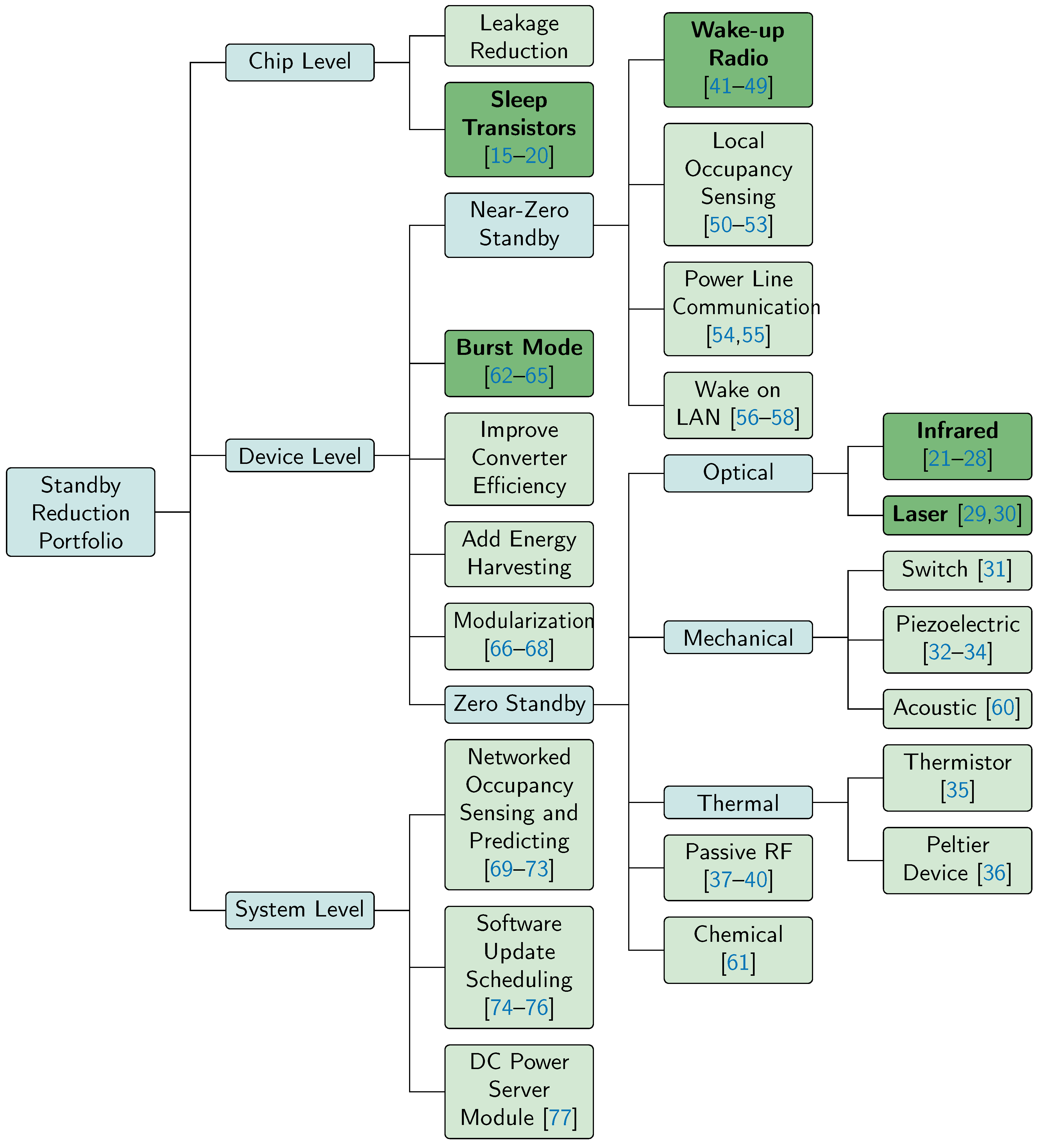
1.3. A Portfolio of Standby Solutions
1.4. Summary
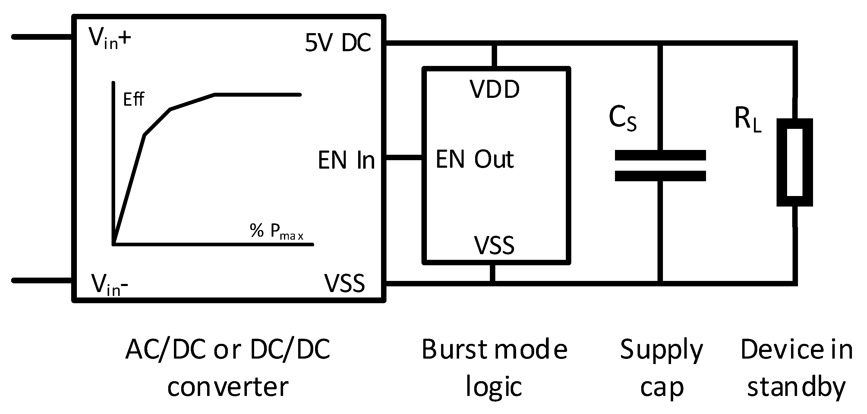
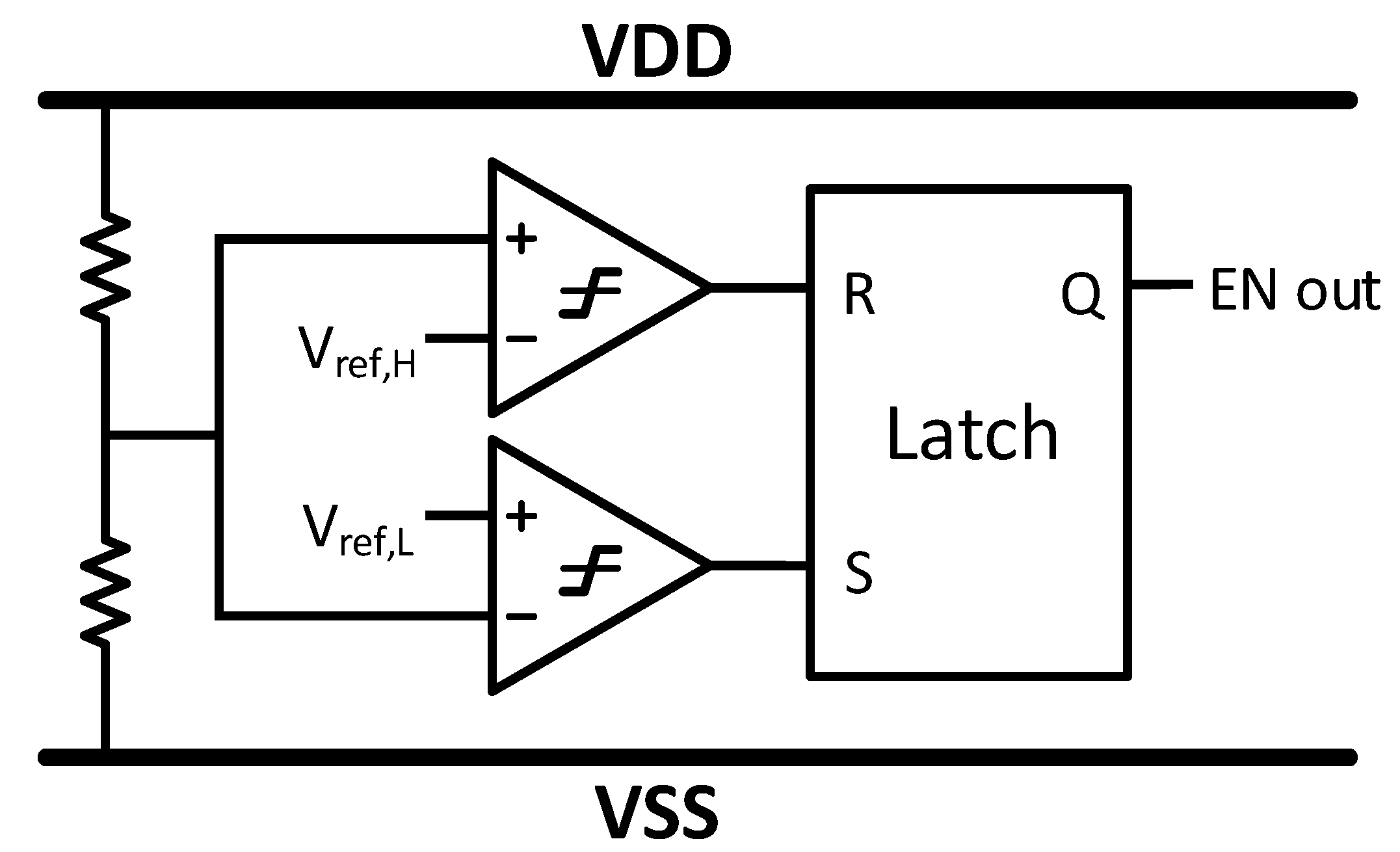
2. Burst Mode
2.1. Description
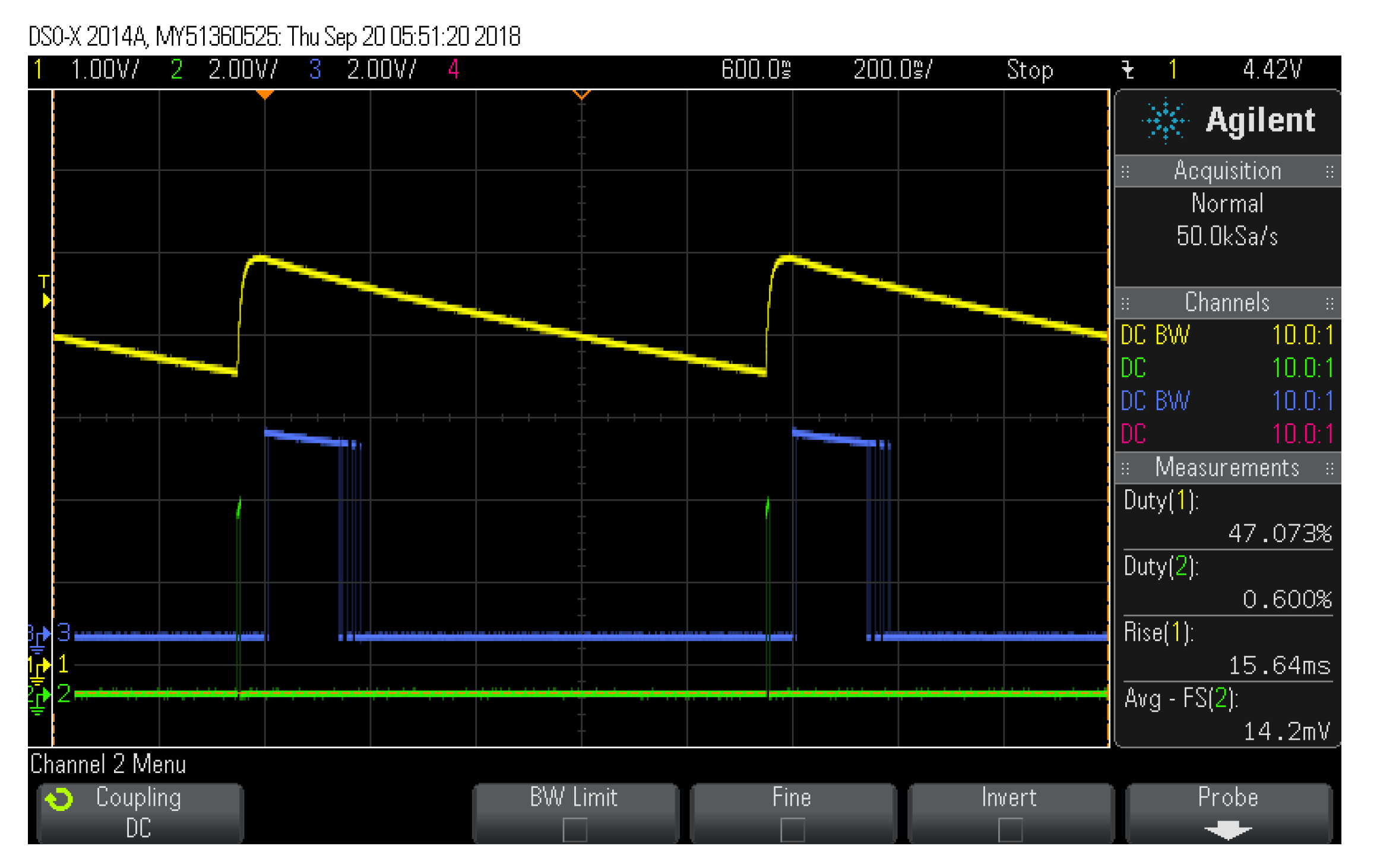
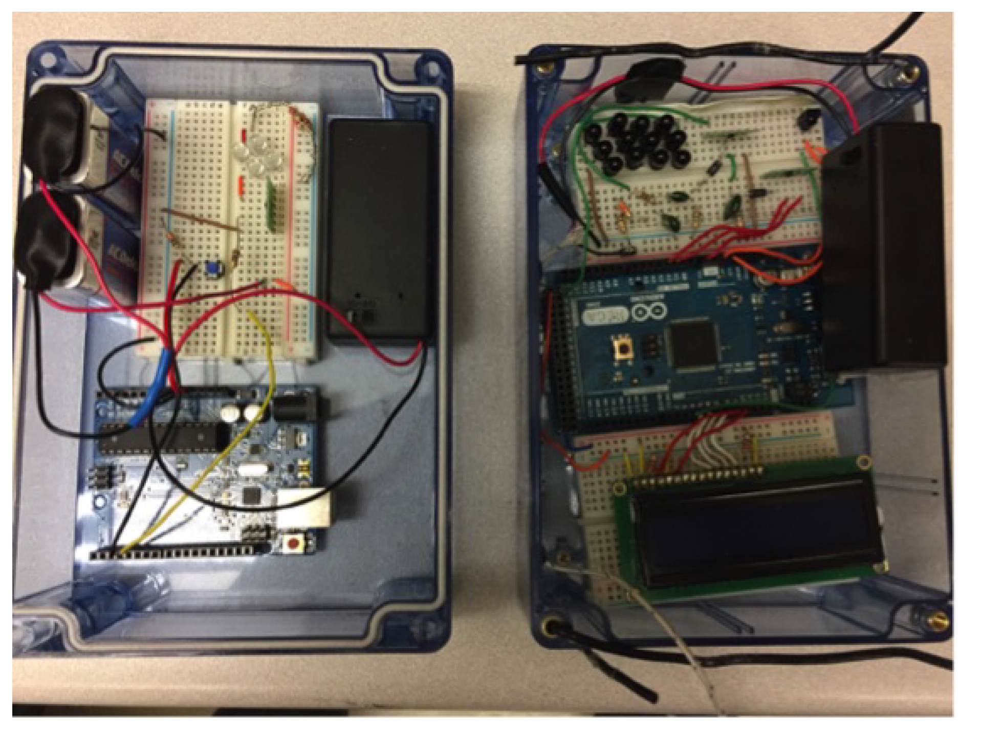
2.2. Experimental Results
3. Sleep Transistors
3.1. General Background
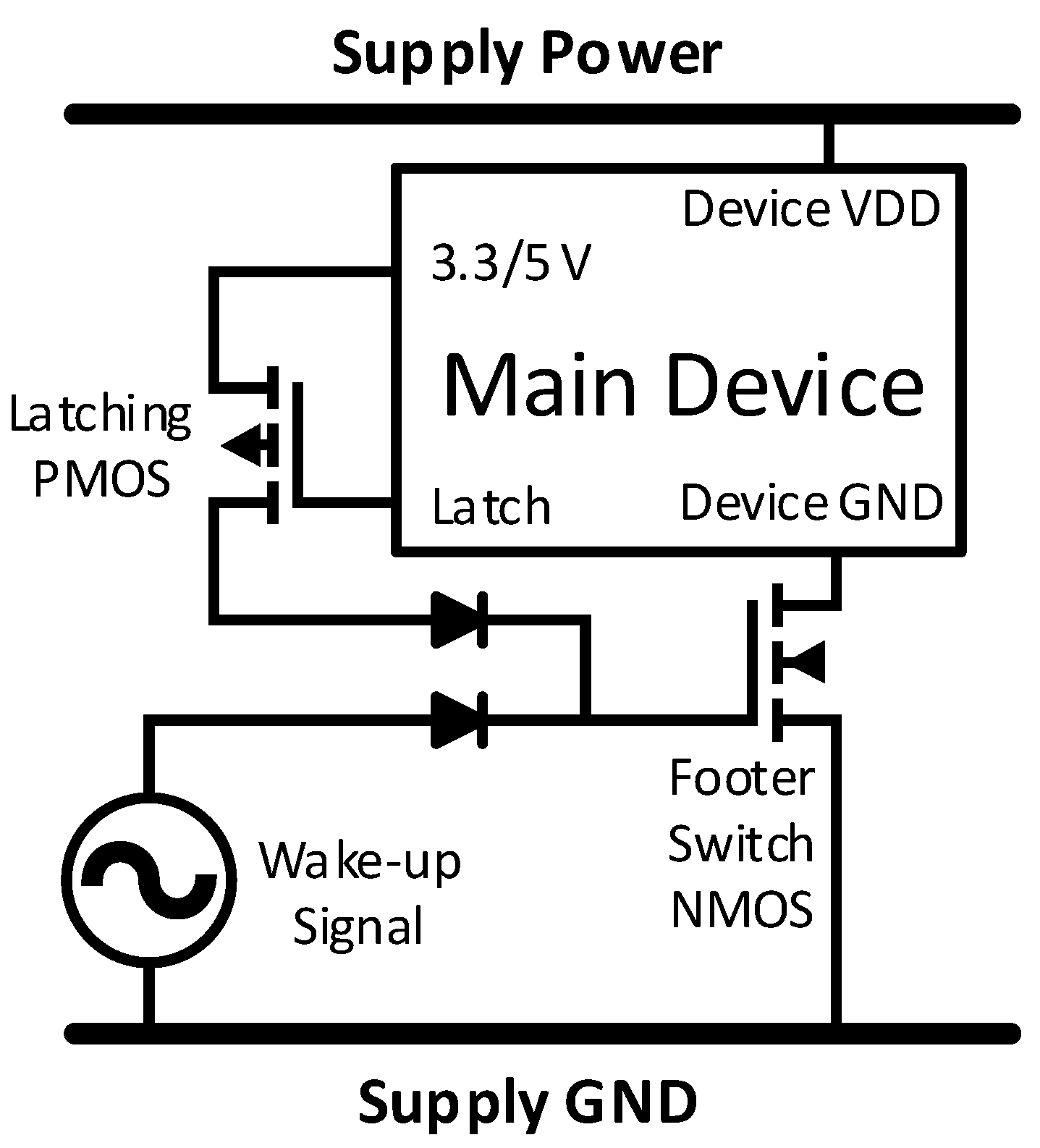
3.2. Footer Switch
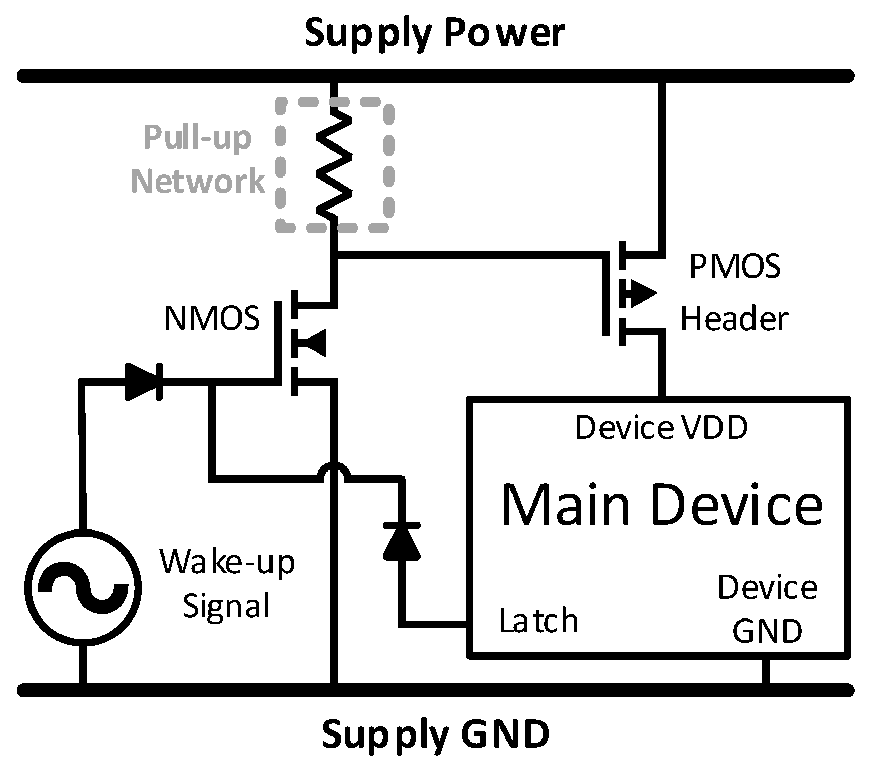
3.3. Header Switch
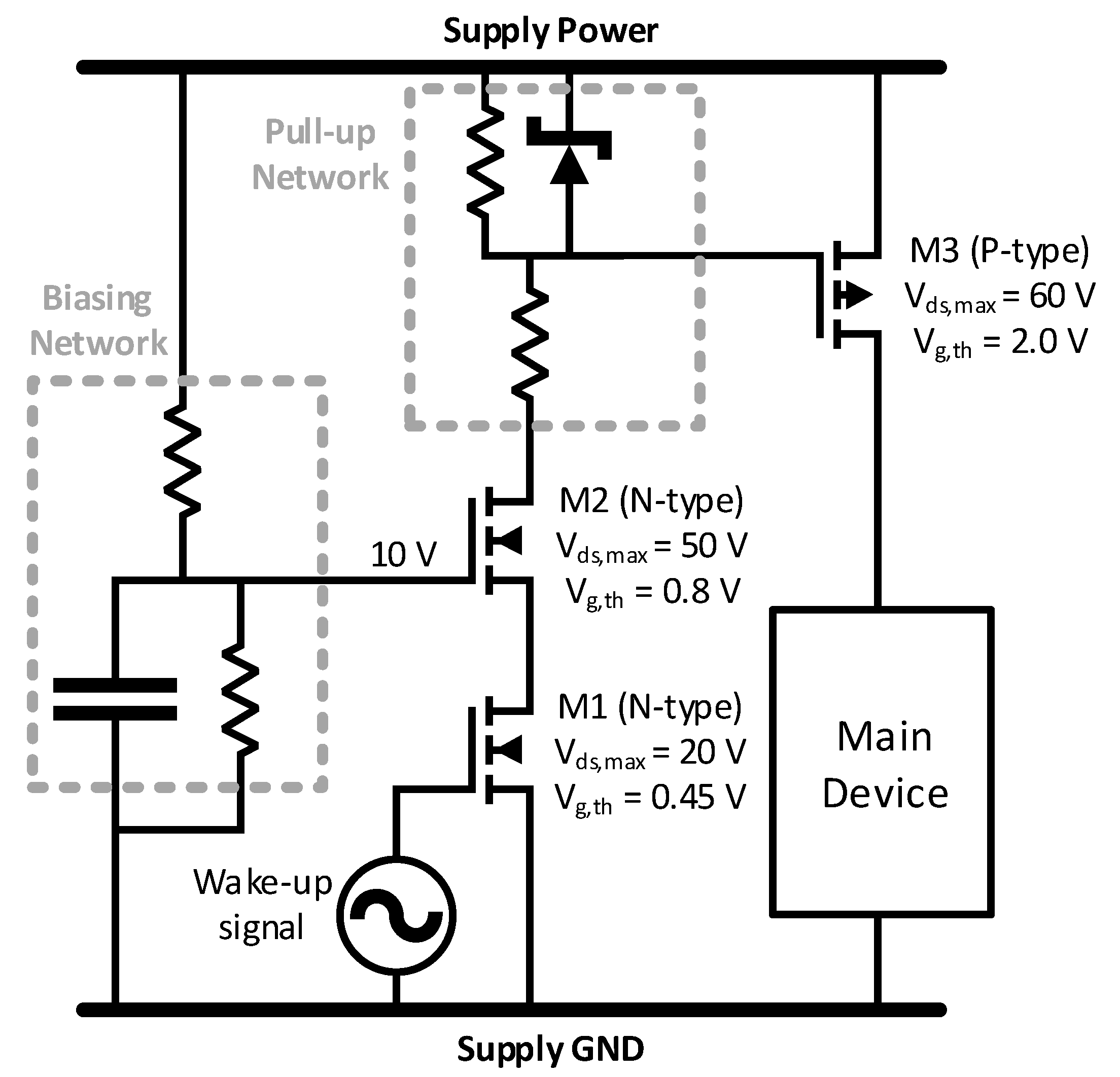
3.4. Cascoded Header Switch
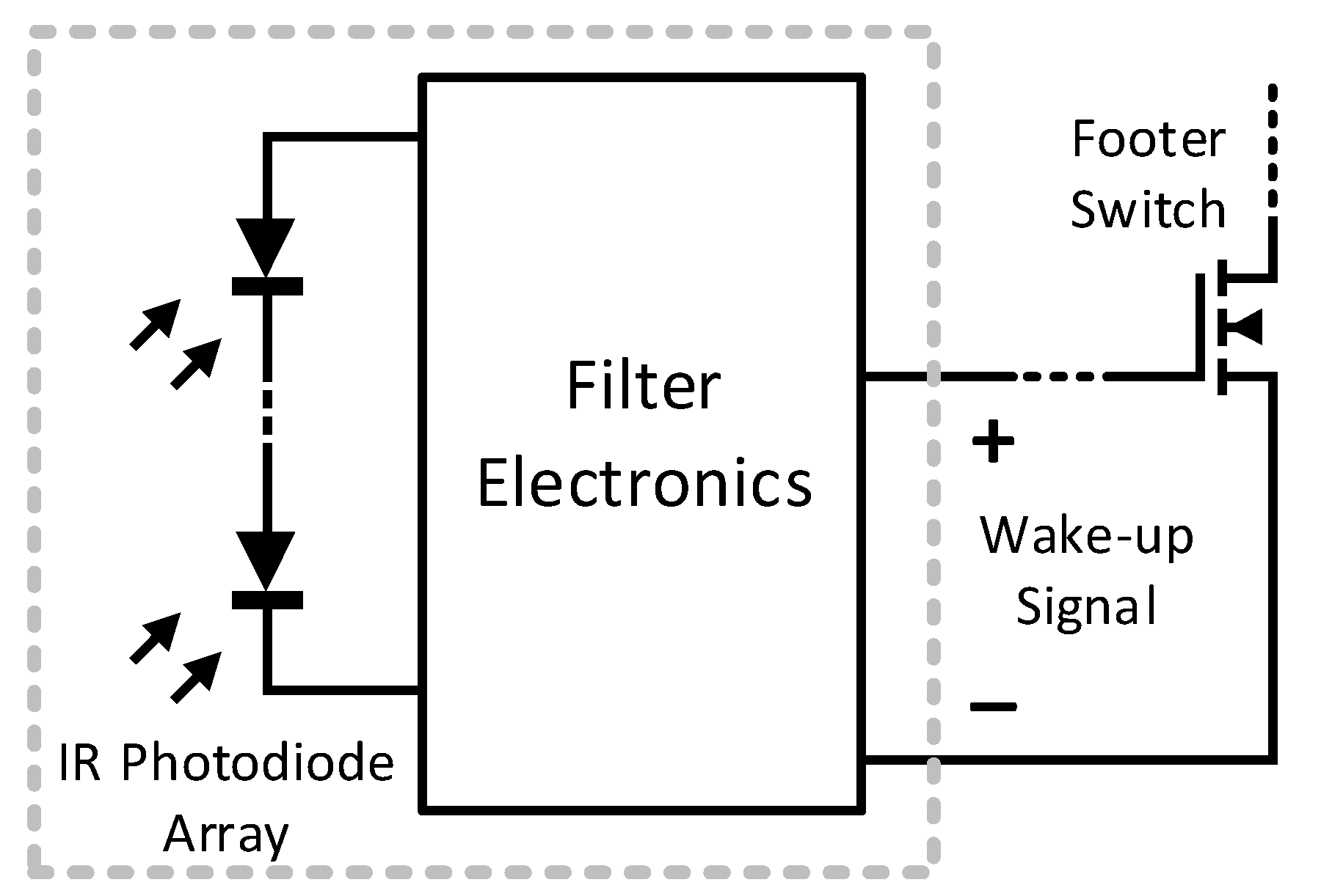
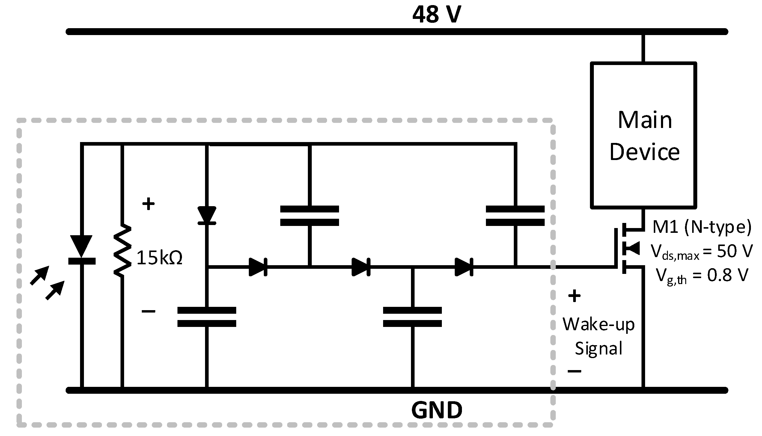
4. Optical Wake-Up Signal
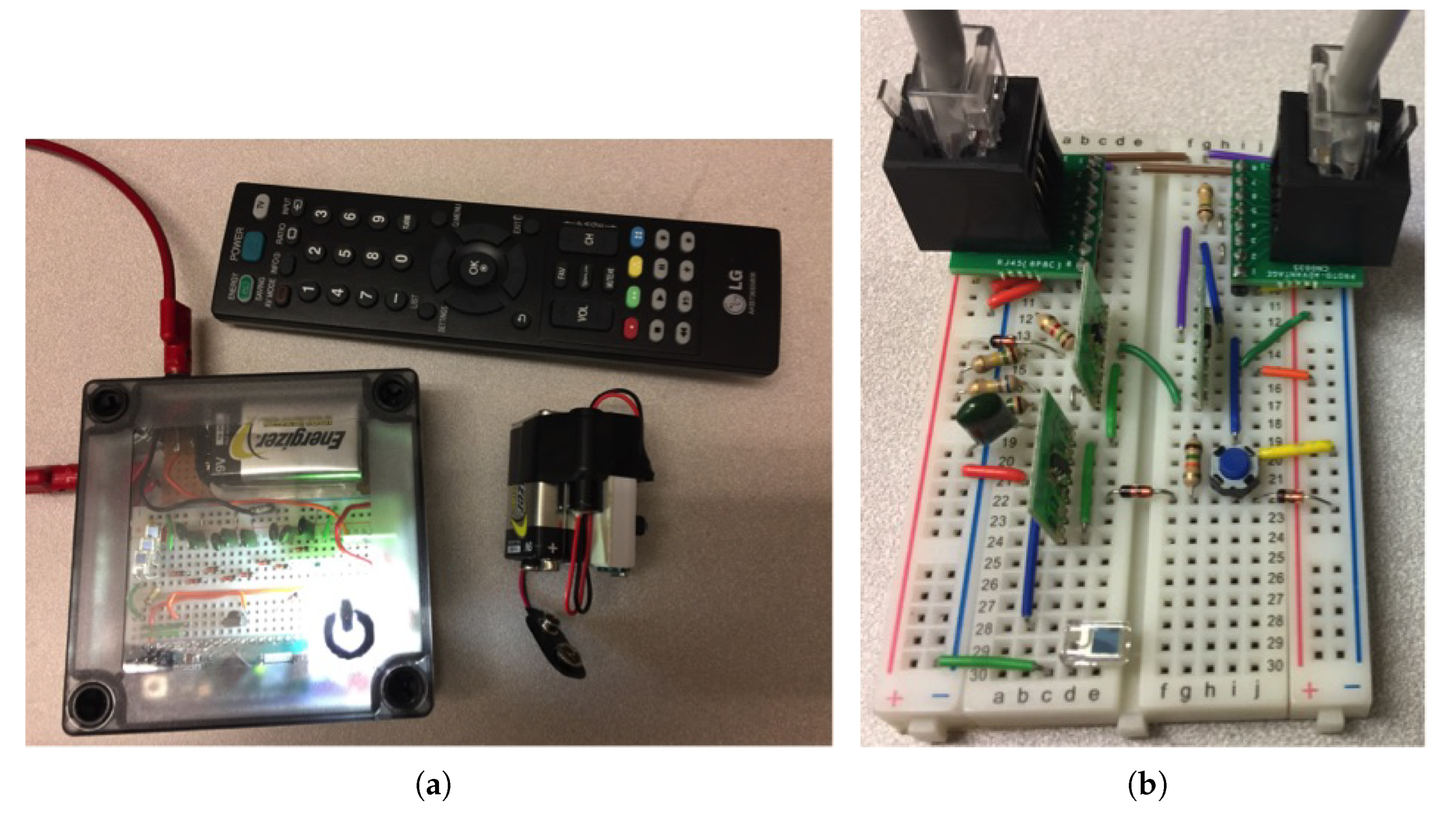
4.1. Infrared Wake-Up Signal
4.2. Laser Wake-Up Signal
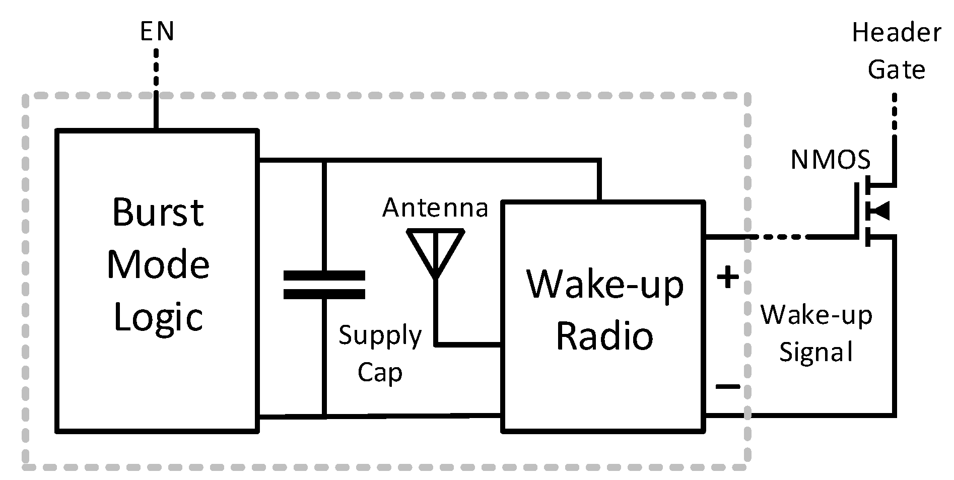
5. Wake-Up Radio
6. Conclusions
Author Contributions
Acknowledgments
Conflicts of Interest
References
- IEA. Things that Go Blip in the Night: Standby Power and How to Limit It; Technical Report; International Energy Agency: Paris, France, 2001. [Google Scholar]
- Urban, B.; Tiefenbeck, V.; Roth, K. Energy Consumption of Consumer Electronics in US Homes in 2010; Fraunhofer Center for Sustainable Energy Systems: Boston, MA, USA, 2011. [Google Scholar]
- Delforge, P.; Schmidt, L.; Schmidt, S. Home Idle Load: Devices Wasting Huge Amounts of Electricity When Not in Active Use; NRDC Issue Paper IP:15-03-A; Natural Resources Defense Council: San Francisco, CA, USA, 2015. [Google Scholar]
- Lu, T.K.; Yeh, C.T.; Chang, W.C. Measuring the use of residential standby power in Taiwan. Energy Build. 2011, 43, 3539–3547. [Google Scholar] [CrossRef]
- De Almeida, A.T.; Patrao, C.; Riviere, P.; Da Silva, D.; Schlomann, B.; Gigli, M.; Harrison, B. Standby and off-mode power demand of new appliances in the market. In Proceedings of the 6th International Conference on Energy Efficiency in Domestic Appliances and Lighting (EEDAL’11), Copenhague, Danemark, 24–26 May 2011; p. 12. [Google Scholar]
- Clement, K.; Pardon, I.; Driesen, J. Standby power consumption in Belgium. In Proceedings of the 9th International Conference on Electrical Power Quality and Utilisation (EPQU 2007), Piscataway, NJ, USA, 9–11 October 2007; pp. 1–4. [Google Scholar]
- Sahin, M.C.; Aydinalp Koksal, M. Standby electricity consumption and saving potentials of Turkish households. Appl. Energy 2014, 114, 531–538. [Google Scholar] [CrossRef]
- Ahmadi-Karvigh, S.; Ghahramani, A.; Becerik-Gerber, B.; Soibelman, L. Real-time activity recognition for energy efficiency in buildings. Appl. Energy 2018, 211, 146–160. [Google Scholar] [CrossRef]
- IEA. More Data, Less Energy: Making Network Standby More Efficient in Billions of Connected Devices; Technical Report; IEA: Paris, France, 2014. [Google Scholar]
- Comstock, O.; Jarzomski, K. Consumption and saturation trends of residential miscellaneous end-use loads. In Proceedings of the 2012 ACEEE Summer Study Energy Efficiency Buildings, Pacific Grove, CA, USA, 12–17 August 2012. [Google Scholar]
- IEC 62301:2011: Household Electrical Appliances—Measurement of Standby Power; Technical Report; International Electrotechnical Commission Standard: Geneva, Switzerland, 2011.
- Bourassa, N.L.; Rainer, L.; Mai, J.; Curtin, C. Final Standardized Test Bed Specification and Findings Report (Task 5); Technical Report; Lawrence Berkeley National Laboratory: Berkeley, CA, USA, 2018.
- Ellis, M.; Siderius, H.P.; Lane, K. Closing the Gap towards Net Zero Energy Appliances; ECEEE 2015 Summer Study Proceedings; European Council for an Energy-Efficient Economy: Hyères, France, 2015. [Google Scholar]
- Meier, A.; Siderius, H.P. Should the Next Standby Power Target Be 0-Watt? European Council for an Energy-Efficient Economy: Hyeres, France, 2017. [Google Scholar]
- Jiang, H.; Marek-Sadowska, M.; Nassif, S.R. Benefits and costs of power-gating technique. In Proceedings of the 2005 IEEE International Conference on Computer Design: VLSI in Computers and Processors, San Jose, CA, USA, 2–5 October 2005; pp. 559–566. [Google Scholar]
- Shi, K.; Howard, D. Challenges in sleep transistor design and implementation in low-power designs. In Proceedings of the 43rd Annual Design Automation Conference, San Francisco, CA, USA, 24–28 July 2006; pp. 113–116. [Google Scholar]
- Long, C.; He, L. Distributed sleep transistor network for power reduction. IEEE Trans. Very Large Scale Integr. VLSI Syst. 2004, 12, 937–946. [Google Scholar] [CrossRef]
- Fallah, F.; Pedram, M. Standby and active leakage current control and minimization in CMOS VLSI circuits. IEICE Trans. Electron. 2005, 88, 509–519. [Google Scholar] [CrossRef]
- Fukuoka, K.; Maeda, N.; Nii, K.; Fujigaya, M.; Sakamoto, N.; Koike, T.; Irita, T.; Wakahara, K.; Matsuyama, T.; Hasegawa, K.; et al. Power-Management Features of R-Mobile U2, an Integrated Application Processor and Baseband Processor. IEEE Micro 2013, 33, 26–36. [Google Scholar] [CrossRef]
- Chao, B.; Harrison, L. Re-Designing Normally-on Load Switches with Zero-Power Mosfets Reduces Power Consumption; Advanced Linear Devices: Sunnyvale, CA, USA, 2008. [Google Scholar]
- Yamawaki, A.; Serikawa, S. Power supply circuit with zero standby power consumption on infrared remote controlled product by using energy harvesting. In Proceeding of the International MultiConference of Engineers and Computer Scientists, Hong Kong, China, 18–20 March 2015; Volume 2, p. 00002. [Google Scholar]
- Park, K.H.; Yi, K.H. Cost-effective power system with an electronic double layer capacitor for reducing the standby power consumption of consumer electronic devices. J. Power Electron. 2013, 13, 362–368. [Google Scholar] [CrossRef]
- Koidea, D.; Yoshikawaa, K.; Yamawakia, A. Remote power strip with zero standby power controllable from every direction. In Proceeding of the ICISIP 2015: The 3rd IIAE International Conference on Intelligent Systems and Image Processing, Fukuoka, Japan, 2–5 September 2015. [Google Scholar]
- Reshma, A.R. Standby Power Reduction System. Int. J. Eng. Innov. Technol. 2014, 4, 139–142. [Google Scholar]
- Rosa, R.L.; Aiello, N.; Zoppi, G. An Innovative System Capable to Turn on Any Turned off electrical appliance by means of an efficient optical energy transfer. In Proceedings of the International Exhibition and Conference for Power Electronics, Intelligent Motion, Renewable Energy and Energy Management, Nuremberg, Germany, 20–22 May 2014; pp. 1–8. [Google Scholar]
- Utsunomiya, F.; Tanaka, A.; Douseki, T. A self-powered photosensor switch detects only rising edge of infrared-light pulse for wireless zero-standby-power wake-up receiver. In Proceedings of the 2013 IEEE SENSER, Baltimore, MD, USA, 3–6 November 2013; pp. 1–4. [Google Scholar] [CrossRef]
- Rajaram, V.; Qian, Z.; Kang, S.; Cassella, C.; McGruer, N.E.; Rinaldi, M. Microelectromechanical detector of infrared spectral signatures with near-zero standby power consumption. In Proceeding of the 19th International Conference on Solid-State Sensors, Actuators and Microsystems (TRANSDUCERS), Kaohsiung, Taiwan, 18–22 June 2017; pp. 846–849. [Google Scholar] [CrossRef]
- Qian, Z.; Kang, S.; Rajaram, V.; Cassella, C.; McGruer, N.E.; Rinaldi, M. Zero-power infrared digitizers based on plasmonically enhanced micromechanical photoswitches. Nat. Nanotechnol. 2017, 12, 969–973. [Google Scholar] [CrossRef]
- Kang, S.; Park, K.; Shin, S.; Chang, K.; Kim, H. Zero Standby Power Remote Control System Using Light Power Transmission. IEEE Trans. Consum. Electron. 2011, 57, 1622–1627. [Google Scholar] [CrossRef]
- Gerber, D.L.; Meier, A.; Hosbach, R.; Liou, R. Zero Standby Solutions with Optical Energy Harvesting from a Laser Pointer. Electronics 2018, 7, 292. [Google Scholar] [CrossRef]
- Tsai, C.H.; Bai, Y.W.; Lin, M.B.; Jhang, R.J.R.; Chung, C.Y. Reduce the standby power consumption of a microwave oven. IEEE Trans. Consum. Electron. 2013, 59, 54–61. [Google Scholar] [CrossRef]
- Shibasaki, K.; Kono, S.; Yamawaki, A. An Architecture of Energy Efficient Restroom by Making Zero Standby Power. In Proceedings of the 5th IIAE International Conference on Industrial Application Engineering, Kitakyushu, Japan, 27–31 March 2017; pp. 323–326. [Google Scholar]
- Yamawaki, A.; Serikawa, S. Applying sensor node with zero standby power to door monitor. In Proceedings of the International MultiConference of Engineers and Computer Scientists 2016, Hong Kong, China, 16–18 March 2016; pp. 2183–2187. [Google Scholar]
- Takaichi, Y.; Koide, D.; Yamawaki, A. Wake-up time Measurement of Wireless Sensor Node with Zero Standby-power. In Proceedings of the 4th IIAE International Conference on Intelligent Systems and Image Processing 2016, Kyoto, Japan, 8–12 September 2016; pp. 225–228. [Google Scholar] [CrossRef]
- Chalko, T. A fridge that takes only 0.1 kWh a day? Renew (Australia) 2005, 90, 36–40. [Google Scholar]
- Kuwatani, T.; Takaichi, Y.; Yamawaki, A. A Fire Alarm Sensor Node with Long Battery Life by Zero Standby Power Consumption. In Proceedings of the 5th IIAE International Conference on Industrial Application Engineering, Kitakyushu, Japan, 27–31 March 2017; pp. 327–330. [Google Scholar] [CrossRef]
- Zhang, L.; Jiang, H.; Sun, X.; Zhang, C.; Wang, Z. A passive RF receiving and power switch ASIC for remote power control with zero stand-by power. In Proceedings of the IEEE Asian Solid-State Circuits Conference, Fukuoka, Japan, 3–5 November 2008; pp. 109–112. [Google Scholar]
- Chen, L.; Wang, Z.; Jia, C.; Li, F.; Hao, W.; Xiao, B.; Zhang, C.; Wang, Z. A RF remote-control transceiver with zero-standby power based on RFID technology. Electronics 2010, 243–246. [Google Scholar]
- Siwamogsatham, S.; Rattanawan, P.; Kitjaroen, M.; Songtung, P.; Pongpaibool, P.; Navanugraha, K. Smartly saving energy with a zero power consumption standby system. In Proceedings of the 2011 Proceedings of PICMET ’11: Technology Management in the Energy Smart World (PICMET), Portland, OR, USA, 31 July–4 August 2011; pp. 1–4. [Google Scholar]
- Mozar, S.; Funabiki, N. Switching System, a Zero Power Standby Solution. Int. J. Eng. Res. Sci. 2017, 3, 2395–6992. [Google Scholar]
- Demirkol, I.; Ersoy, C.; Onur, E. Wake-up receivers for wireless sensor networks: benefits and challenges. IEEE Wirel. Commun. 2009, 16, 88–96. [Google Scholar] [CrossRef]
- Magno, M.; Marinkovic, S.; Srbinovski, B.; Popovici, E.M. Wake-up radio receiver based power minimization techniques for wireless sensor networks: A review. Microelectron. J. 2014, 45, 1627–1633. [Google Scholar] [CrossRef]
- Umeda, T.; Otaka, S. ECO chip: Energy consumption zeroize chip with a 953MHz high-sensitivity radio wave detector for standby mode applications. In Proceedings of the Custom Integrated Circuits Conference, San Jose, CA, USA, 16–19 September 2007; pp. 663–666. [Google Scholar]
- Gamm, G.U.; Sippel, M.; Kostic, M.; Reindl, L.M. Low power wake-up receiver for wireless sensor nodes. In Proceedings of the 2010 Sixth International Conference on Intelligent Sensors, Sensor Networks and Information Processing (ISSNIP), Brisbane, Australia, 7–10 December 2010; pp. 121–126. [Google Scholar]
- Oller, J.; Demirkol, I.; Casademont, J.; Paradells, J.; Gamm, G.U.; Reindl, L. Performance evaluation and comparative analysis of subcarrier modulation wake-up radio systems for energy-efficient wireless sensor networks. Sensors 2013, 14, 22–51. [Google Scholar] [CrossRef]
- Jiang, H.; Wang, P.P.; Gao, L.; Sen, P.; Kim, Y.; Rebeiz, G.M.; Hall, D.A.; Mercier, P.P. 24.5 A 4.5 nW wake-up radio with −69 dBm sensitivity. In Proceedings of the 2017 IEEE International Solid-State Circuits Conference (ISSCC), San Francisco, CA, USA, 5–9 February 2017; pp. 416–417. [Google Scholar] [CrossRef]
- Wang, P.P.; Jiang, H.; Gao, L.; Sen, P.; Kim, Y.; Rebeiz, G.M.; Mercier, P.P.; Hall, D.A. A Near-Zero-Power Wake-Up Receiver Achieving −69 dBm Sensitivity. IEEE J. Solid-State Circuits 2018, 53, 1640–1652. [Google Scholar] [CrossRef]
- Moody, J.; Bassirian, P.; Roy, A.; Liu, N.; Pancrazio, S.; Barker, N.S.; Calhoun, B.H.; Bowers, S.M. A −76 dBm 7.4 nW wakeup radio with automatic offset compensation. In Proceedings of the 2018 IEEE International Solid-State Circuits Conference (ISSCC), San Francisco, CA, USA, 11–15 February 2018; pp. 452–454. [Google Scholar] [CrossRef]
- Bassirian, P.; Moody, J.; Lu, R.; Gao, A.; Manzaneque, T.; Roy, A.; Barker, N.S.; Calhoun, B.H.; Gong, S.; Bowers, S.M. Nanowatt-Level Wakeup Receiver Front Ends Using MEMS Resonators for Impedance Transformation. IEEE Trans. Microwave Theory Tech. 2019, 67, 1615–1627. [Google Scholar] [CrossRef]
- Tsai, C.H.; Bai, Y.W.; Lin, M.B.; Jhang, R.R.; Lin, Y.W. Design and implementation of a PIR luminaire with zero standby power using a photovoltaic array in enough daylight. IEEE Trans. Consum. Electron. 2013, 59, 499–506. [Google Scholar] [CrossRef]
- Tsai, C.H.; Bai, Y.W.; Chu, C.A.; Chung, C.Y.; Lin, M.B. Design and implementation of a socket with zero standby power using a photovoltaic array. IEEE Trans. Consum. Electron. 2010, 56, 2686–2693. [Google Scholar] [CrossRef]
- Tsai, C.H.; Bai, Y.W.; Cheng, L.C.; Lin, K.S.; Jhang, R.J.R.; Lin, M.B. Reducing the standby power consumption of a pc monitor. In Proceedings of the 1st IEEE Global Conference on Consumer Electronics, Las Vegas, NV, USA, 11 September 2012; pp. 520–524. [Google Scholar]
- Tsai, C.H.; Bai, Y.W.; Chen, P.C.; Jhang, R.J.R.; Lin, M.B. Reduction of the standby power consumption of an automatic door system. In Proceedings of the 2016 IEEE International Conference on Consumer Electronics (ICCE), Las Vegas, NV, USA, 9–11 Janurary 2016; pp. 583–584. [Google Scholar]
- Golchin, P.; Tosato, P.; Brunelli, D. Design optimization of zero power wake-up receiver in Power line communication. In Proceedings of the 2016 International Symposium on Power Electronics, Electrical Drives, Automation and Motion (SPEEDAM), Anacapri, Italy, 22–24 June 2016; pp. 564–569. [Google Scholar] [CrossRef]
- Golchin, P.; Tosato, P.; Brunelli, D. Zero-energy wake up for power line communications in smart cities. In Proceedings of the 2016 IEEE International Smart Cities Conference (ISC2), Trento, Italy, 12–15 September 2016; pp. 1–6. [Google Scholar] [CrossRef]
- Mishra, N.; Chebrolu, K.; Raman, B.; Pathak, A. Wake-on-WLAN. In Proceedings of the 15th International Conference on World Wide Web, New York, NY, USA, 23–26 May 2006; pp. 761–769. [Google Scholar]
- Ricciardi, S.; Santos-Boada, G.; Careglio, D.; Palmieri, F.; Fiore, U. Evaluating energy savings in WoL-enabled networks of PCs. In Proceedings of the 2013 IEEE International Symposium on Industrial Electronics, Taipei, Taiwan, 28–31 May 2013; pp. 1–6. [Google Scholar] [CrossRef]
- Lieberman, P. White Paper: Wake on Lan Technology; Lieberman Software Corporation: Los Angeles, CA, USA, 2006. [Google Scholar]
- Olsson, R.H.; Bogoslovov, R.B.; Gordon, C. Event driven persistent sensing: Overcoming the energy and lifetime limitations in unattended wireless sensors. In Proceedings of the 2016 IEEE SENSORS, Orlando, FL, USA, 30 October–2 November 2016; pp. 1–3. [Google Scholar] [CrossRef]
- Jeong, S.; Chen, Y.; Jang, T.; Tsai, J.; Blaauw, D.; Kim, H.; Sylvester, D. 21.6 A 12nW always-on acoustic sensing and object recognition microsystem using frequency-domain feature extraction and SVM classification. In Proceedings of the 2017 IEEE International Solid-State Circuits Conference (ISSCC), San Francisco, CA, USA, 5–9 February 2017; pp. 362–363. [Google Scholar] [CrossRef]
- Banerjee, A.; Farhoudi, N.; Ghosh, C.; Mastrangelo, C.H.; Kim, H.; Broadbent, S.J.; Looper, R. Picowatt gas sensing and resistance switching in tunneling nano-gap electrodes. In Proceedings of the 2016 IEEE SENSORS, Orlando, FL, USA, 30 October–2 November 2016; pp. 1–3. [Google Scholar] [CrossRef]
- Lo, Y.K.; Yen, S.C.; Lin, C.Y. A high-efficiency AC-to-DC adaptor with a low standby power consumption. IEEE Trans. Ind. Electron. 2008, 55, 963–965. [Google Scholar] [CrossRef]
- Lee, K.; Sung, C.; Yoon, H.; Kang, B. Improvement of power-conversion efficiency at light-load using a variable-duty burst mode. In Proceedings of the Power and Energy Conference at Illinois (PECI), Urbana, IL, USA, 22–23 February 2013; pp. 142–146. [Google Scholar]
- Kim, B.C.; Park, K.B.; Moon, G.W. Sawtooth burst mode control with minimum peak current in stand-by operation of power supply. In Proceedings of the 2011 IEEE 8th International Conference on Power Electronics and ECCE Asia (ICPE & ECCE), Jeju, Korea, 30 May–3 June 2011; pp. 474–479. [Google Scholar]
- Choi, J.-H.; Huh, D.-Y.; Kim, Y.-S. The improved burst mode in the stand-by operation of power supply. APEC-04 2004, 1, 426–432. [Google Scholar]
- Kim, J.; Jung, E.S.; Lee, Y.T.; Ryu, W. An implementation of energy-saving set-top box. In Proceedings of the 2015 International Conference on Information and Communication Technology Convergence (ICTC), Jeju Island, Korea, 28–30 October 2015; pp. 793–796. [Google Scholar]
- Huang, T.; Bai, Y.W.; Chao, S.K. Reducing the system standby power of a personal computer. IET Comput. Digital Tech. 2015, 9, 248–258. [Google Scholar] [CrossRef]
- Agarwal, Y.; Hodges, S.; Chandra, R.; Scott, J.; Bahl, V.; Gupta, R. Somniloquy: Augmenting network interfaces to reduce PC energy usage. In Proceedings of the NSDI 2009: 6th USENIX Symposium on Networked Systems Design and Implementation, Boston, MA, USA, 22–24 Aprial 2009. [Google Scholar]
- Bai, Y.W.; Ku, Y.T. Automatic room light intensity detection and control using a microprocessor and light sensors. IEEE Trans. Consum. Electron. 2008, 54, 1173–1176. [Google Scholar] [CrossRef]
- Pompermayer, D.C.; Có, M.A.; Donadel, C.B. Design and implementation of a low-cost intelligent device to standby mode consumption reduction in already existing electrical equipment. IEEE Trans. Consum. Electron. 2017, 63, 145–152. [Google Scholar] [CrossRef]
- Byun, J.; Park, S.; Kang, B.; Hong, I.; Park, S. Design and implementation of an intelligent energy saving system based on standby power reduction for a future zero-energy home environment. IEEE Trans. Consum. Electron. 2013, 59, 507–514. [Google Scholar] [CrossRef]
- Heo, J.; Hong, C.S.; Kang, S.B.; Jeon, S.S. Design and implementation of control mechanism for standby power reduction. In Proceedings of the 2008 Second International Conference on Electrical Engineering, Hoi An City, Vietnam, 4–6 June 2008; pp. 1–2. [Google Scholar]
- Han, J.; Choi, C.S.; Lee, I. More efficient home energy management system based on ZigBee communication and infrared remote controls. IEEE Trans. Consum. Electron. 2011, 57, 85–89. [Google Scholar]
- Kim, J.; Park, H.; Lee, Y.; Lee, H. An implementation of adaptively power-managed set-top box. In Proceedings of the 2016 International Conference on Information and Communication Technology Convergence (ICTC), Jeju Island, Korea, 19–21 October 2016; pp. 855–858. [Google Scholar] [CrossRef]
- Shin, T.; Jeon, H.T.; Byun, J. Developing nontrivial standby power management using consumer pattern tracking for on-demand appliance energy saving over cloud networks. IEEE Trans. Consum. Electron. 2016, 62, 251–257. [Google Scholar] [CrossRef]
- Park, H.; Kim, J.; Jung, E.; Kwon, E.; Lee, Y. Network-Assisted Management of Power-Efficient Set-Top Boxes for Enhancing User Experience. IEEE Trans. Consum. Electron. 2018, 64, 2–10. [Google Scholar] [CrossRef]
- Nextek Power Systems. Tech Overview. Nextek Power Systems, Inc. Is A Pioneer in Low-Cost, Energy Efficient Direct Current (DC) Power Generation and Management Networks for Buildings. Available online: https://www.nextekpower.com/tech-overview/ (accessed on 6 December 2018).
- Kim, S.; Vyas, R.; Bito, J.; Niotaki, K.; Collado, A.; Georgiadis, A.; Tentzeris, M.M. Ambient RF energy-harvesting technologies for self-sustainable standalone wireless sensor platforms. Proc. IEEE 2014, 102, 1649–1666. [Google Scholar] [CrossRef]
- Lu, X.; Wang, P.; Niyato, D.; Kim, D.I.; Han, Z. Wireless networks with RF energy harvesting: A contemporary survey. IEEE Commun. Surv. Tutorials 2015, 17, 757–789. [Google Scholar] [CrossRef]


| Load Resistance (Ω) | Average Input Power (mW) | Average Output Power (mW) | Efficiency (%) |
|---|---|---|---|
| 470 | 153.5 | 52.1 | 34.0 |
| 4700 | 95.4 | 5.2 | 5.5 |
| 47,000 | 90.7 | 0.52 | 0.6 |
| Load Resistance (Ω) | Average Input Power (mW) | Average Output Power (mW) | Efficiency (%) |
|---|---|---|---|
| 470 | 80.3 | 36.4 | 45.3 |
| 4700 | 14.9 | 3.9 | 26.0 |
| 47,000 | 8.5 | 0.4 | 4.6 |
| Load Resistance (Ω) | Average Input Power (mW) | Average Output Power (mW) | Efficiency (%) |
|---|---|---|---|
| 470 | 528.0 | 52.7 | 10.0 |
| 4700 | 476.1 | 5.3 | 1.1 |
| 47,000 | 473.6 | 0.5 | 0.1 |
| Load Resistance (Ω) | Average Input Power (mW) | Average Output Power (mW) | Efficiency (%) |
|---|---|---|---|
| 470 | 177.5 | 36.8 | 20.7 |
| 4700 | 44.2 | 3.8 | 8.6 |
| 47,000 | 29.5 | 0.4 | 1.3 |
© 2019 by the authors. Licensee MDPI, Basel, Switzerland. This article is an open access article distributed under the terms and conditions of the Creative Commons Attribution (CC BY) license (http://creativecommons.org/licenses/by/4.0/).
Share and Cite
Gerber, D.L.; Meier, A.; Liou, R.; Hosbach, R. Emerging Zero-Standby Solutions for Miscellaneous Electric Loads and the Internet of Things. Electronics 2019, 8, 570. https://doi.org/10.3390/electronics8050570
Gerber DL, Meier A, Liou R, Hosbach R. Emerging Zero-Standby Solutions for Miscellaneous Electric Loads and the Internet of Things. Electronics. 2019; 8(5):570. https://doi.org/10.3390/electronics8050570
Chicago/Turabian StyleGerber, Daniel L., Alan Meier, Richard Liou, and Robert Hosbach. 2019. "Emerging Zero-Standby Solutions for Miscellaneous Electric Loads and the Internet of Things" Electronics 8, no. 5: 570. https://doi.org/10.3390/electronics8050570
APA StyleGerber, D. L., Meier, A., Liou, R., & Hosbach, R. (2019). Emerging Zero-Standby Solutions for Miscellaneous Electric Loads and the Internet of Things. Electronics, 8(5), 570. https://doi.org/10.3390/electronics8050570