Article

Emerging Zero-Standby Solutions for Miscellaneous Electric Loads and the Internet of Things

1
Building Technology Urban Systems, Lawrence Berkeley National Lab, Berkeley, CA 94720, USA
2
Electrical Engineering Computer Science, University of California, Berkeley, CA 94720, USA
*
Author to whom correspondence should be addressed.
Electronics 2019, 8(5), 570; https://doi.org/10.3390/electronics8050570
Submission received: 17 April 2019 / Revised: 5 May 2019 / Accepted: 16 May 2019 / Published: 23 May 2019
(This article belongs to the Section Power Electronics)

Abstract

:
Despite technical advances in efficiency, devices in standby continue to consume up to 16% of residential electricity. Finding practical, cost-effective reductions is difficult. While the per-unit power consumption has fallen, the number of units continuously drawing power continues to grow. This work reviews a family of technologies that can eliminate standby consumption in many types of electrical plug loads. It also investigates several solutions in detail and develops prototypes. First, burst mode and sleep transistors are established as building blocks for zero-standby solutions. This work then studies the application of two types of wake-up signals. The first is from an optical transmission, and is applicable to remote-controlled devices with a line-of-sight activation, such as set-top boxes, ceiling fans, and motorized curtains. The second is from a wake-up radio, and is applicable to any wireless products. No single technology will address all standby power situations; however, these emerging solutions appear to have broad applicability to save standby energy in miscellaneous plug loads.

1. Introduction

1.1. Background and Motivation for Standby Reduction

Standby power consumption by appliances, electrical devices, and other products continues to represent 3–16% (varies by definition and country) of residential electricity use [1,2,3,4,5,6,7,8]. Considerable progress in reducing standby consumption in specific products has been achieved through a variety of policies and technologies. For example, technical advances in mobile phone chargers, the most visible manifestation of standby consumption, have enabled reductions in off-mode power from more than 2 W in the year 2000 to below 0.3 W today. Most new low-voltage power supplies have standby consumptions below 0.5 W, reflecting minimum energy efficiency standards in Europe, California, and elsewhere [9].
However, the last twenty years has seen an explosion in the number of devices that rely on power supplies and draw power continuously. The growth can be attributed to the proliferation of devices that require direct current (DC) power and/or networking, traditional alternating current (AC)-powered devices that now have electronics, and mobile devices with batteries. Many of these devices fall into the miscellaneous electrical loads (MELs) category, which continues to grow rapidly in terms of both population and energy use [10]. At the same time, many more devices require higher functionality in order to sustain communications. These devices fall into the broad category of the Internet of Things (IoT).
With the increasing number and diversity of electronic products with standby modes, the need to reduce standby power therefore continues to be an important policy and evolving technical challenge. However, as technologies mature, there is a declining potential savings per device, coupled with an increasing number and diversity of electronic products with standby modes. This means that costs of “saving the last watt” must be extraordinarily low to be cost-justified. For reference, saving one watt of continuous power corresponds to only 8.8 kWh/year, or about $1.50 at typical U.S. residential electricity rates.
This work reviews a variety of approaches to further reduce or eliminate standby consumption in plug loads. It then investigates several solutions in detail and develops prototypes. Although IEC 62301:2011 [11] regards a standby power less than 5 mW to be “essentially zero”, this work demonstrates plug-load solutions with less than 10 µW consumption. The tremendous diversity of products with standby means that no single solution is likely to emerge. Instead, a portfolio of widely-applicable solutions presents the best path forward, and this work contributes to that portfolio.

1.2. General Approach to Standby Reduction

The energy consumption behavior of a device can be represented as a histogram of the time it spends in each power mode. As exemplified for a desktop computer in Figure 1, many modern devices operate with long continuous periods in low-power and brief intermittent periods in high-power. The area under the staircase corresponds to the device’s annual energy consumption. Our solutions aim to reduce the power and duration of the standby modes, in a savings strategy referred to as “shrinking the staircase”.
There are several technical strategies for reducing standby consumption. The first is increasing the device’s efficiency at various modes, which lowers overall power consumption. Another technique involves augmenting the device to harvest and store ambient energy, which can be utilized during low-power operation. Finally, modifications in operational design and internal circuitry can greatly reduce or remove consumption at various low-power modes. This paper focuses on the last technique.
In certain applications, a device can operate for a period of time without any grid-supplied power [13]. The duration of this period has been termed the “standzero” time [14]. Many mobile devices already have long standzero times, and the solutions presented in this paper can increase the standzero time in many other types of devices.

1.3. A Portfolio of Standby Solutions

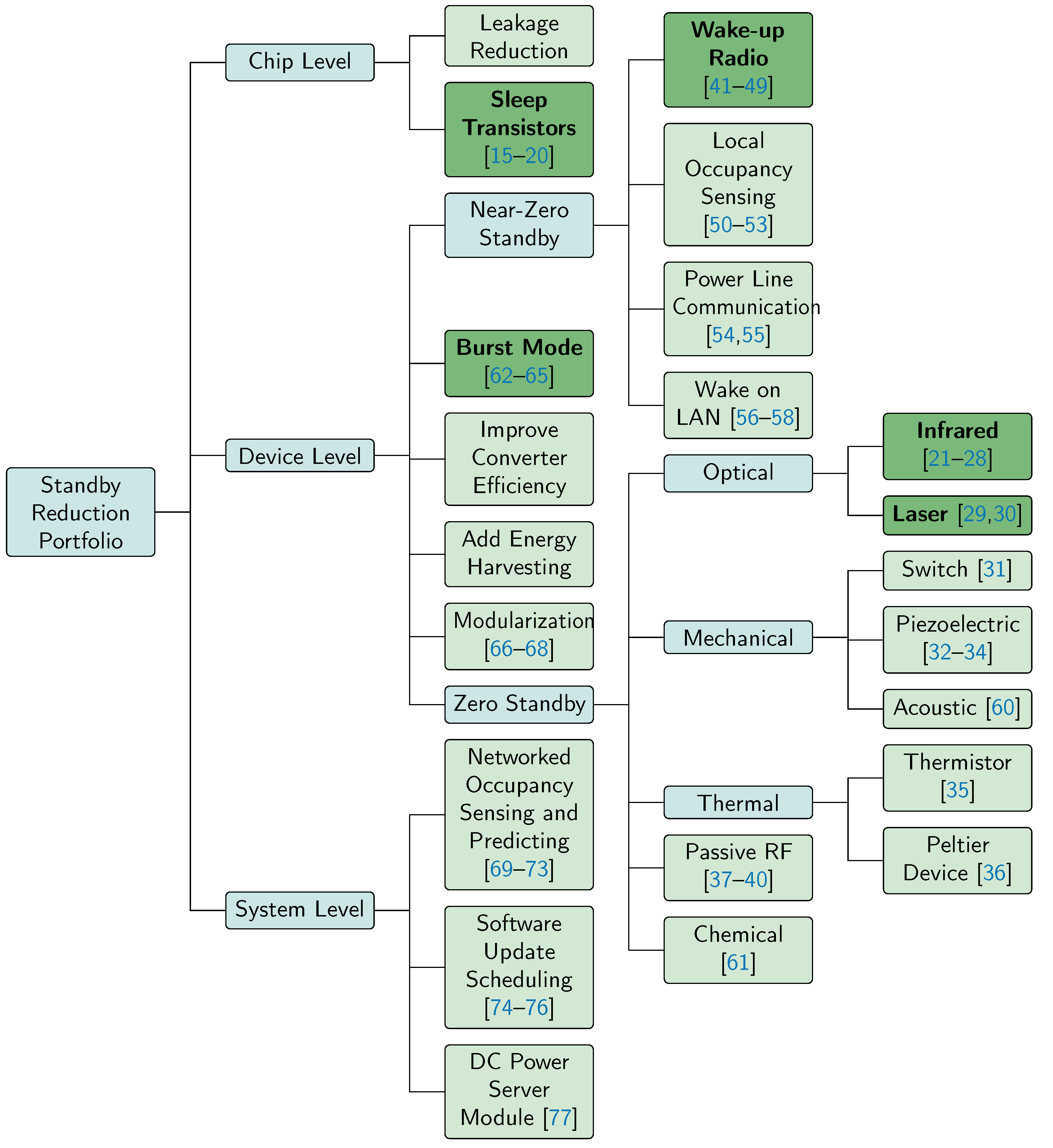
The wide diversity of electronics with standby necessitates development of a portfolio of solutions. Past works propose numerous standby reduction techniques, some of which are shown in Figure 2. These techniques can reduce standby consumption at the chip, device, or system levels.
Some of the chip-level techniques focus on reducing the quiescent power consumption of an integrated circuit (IC). Reducing device leakage can be achieved through improvements to the IC process, or through the use of sleep transistors [15,16,17,18,19,20]. As discussed in Section 3, many of the device-level solutions repurpose the sleep transistor as a discrete solid-state switch.
“Standby-killers” are a family of device-level solutions that use a solid-state switch or mechanical relay to disconnect the device from power when it enters standby. Many of these solutions require an external wake-up signal to activate. Various zero-standby solutions in previous works generate their wake-up signal optically with infrared [21,22,23,24,25,26,27,28] or lasers [29,30], mechanically with switches [31] or piezoelectric devices [32,33,34], thermally with thermistors [35] or peltier devices [36], or through passive RF (radio frequency) transmission [37,38,39,40]. Near-zero standby solutions use an ultra-low-power receiver to process the wake-up signal. These solutions include wake-up radios [41,42,43,44,45,46,47,48,49], occupancy sensors [50,51,52,53], power-line communications [54,55], or wake-on-LAN [56,57,58].
DARPA’s recent N-Zero research program has demonstrated microelectromechanical systems (MEMS) to be a promising alternative to silicon-based standby-killers [59]. N-Zero produced a family of MEMS-based solutions that allow for high sensitivity and sub-microwatt consumption in sensor applications with infrared (IR) [27,28], acoustic [60], chemical [61], and RF [48,49] wake-up methods. Despite their intent for battery-powered sensors, these solutions may also have potential in plug-load applications. Nonetheless, MEMS may experience life span issues due to oxidation or breakdown at the relatively high plug-load voltage.
Other device-level solutions can reduce standby consumption without disconnecting power. Consumption can be reduced at the power converter by improving its efficiency or operating in burst mode [62,63,64,65]. The device can also employ additional energy harvesting and storage to cover standby mode. Finally, the device’s tasks can be modularized and selectively deactivated based on the operation mode [66,67,68].
System-level techniques involve controlling the standby status of multiple devices in a network. Sensing occupancy or predicting user patterns allows a centrally-managed building to selectively turn off unused devices [69,70,71,72,73]. Another prime target for standby reduction is in Internet-connected devices with automatic updates. Future routers could use a scheduling algorithm to allocate time and bandwidth for the update, and deactivate the device when finished [74,75,76]. The final solution is to distribute power through a DC power server module, which can act as a system-wide standby-killer by selectively disabling its ports [77].

1.4. Summary

This work focuses on describing the evaluation of several different standby reduction technologies through analysis and prototypes. Section 2 explains burst mode for power converters and experimentally demonstrates the savings potential. Section 3 describes the operation of sleep transistors such as the footer, header, and cascoded (stacked transistor) header switch. These techniques are used in Section 4 and Section 5 to prototype zero-standby solutions with optical and RF-based wake up signals, respectively.

2. Burst Mode

2.1. Description

Burst mode is a control method for switching power converters that was developed in the early 2000 s to address performance issues in lightly-loaded power converters [62,63,64,65]. Lightly-loaded converters are generally inefficient because of losses in switching, control, and magnetics that are constant regardless of the output power. Burst mode allows a converter to completely deactivate, eliminating its no-load losses. While inactive, the converter powers the load from its output supply capacitor, which must be periodically recharged with a short high-power high-efficiency pulse.
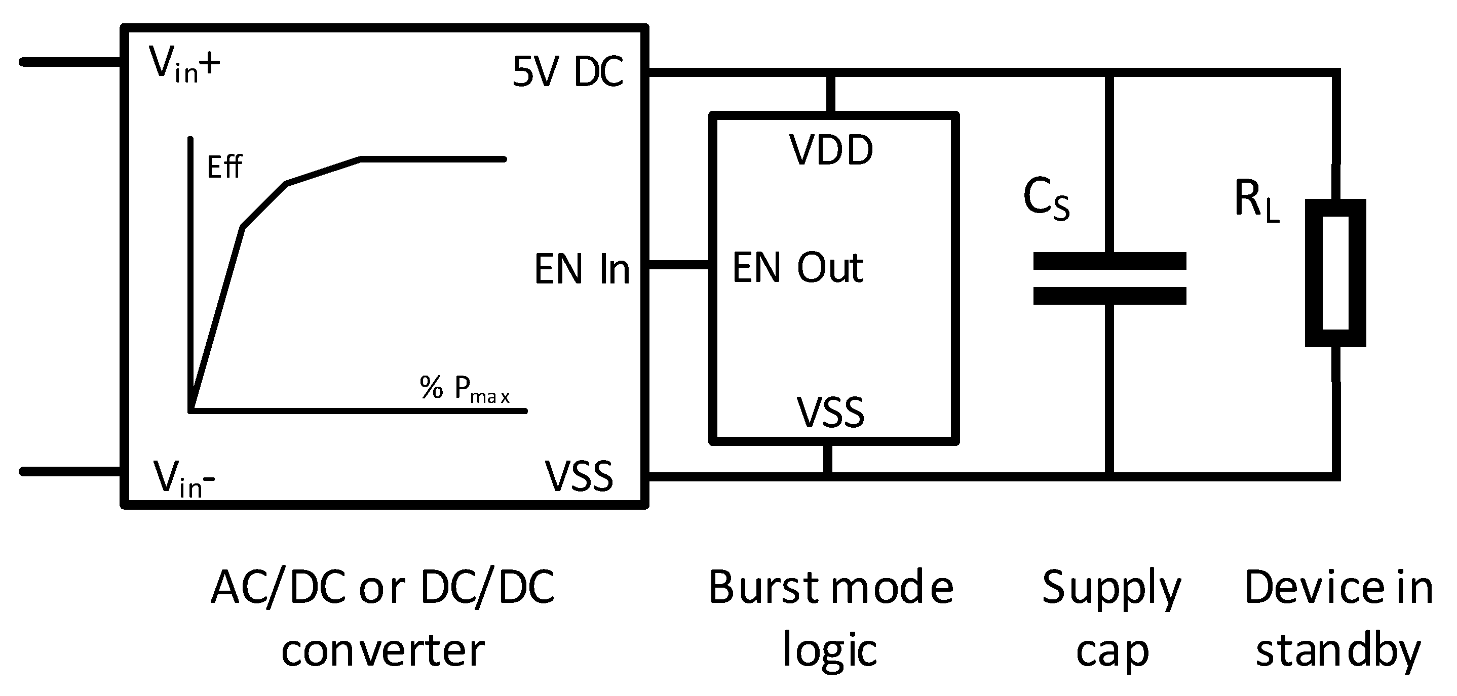
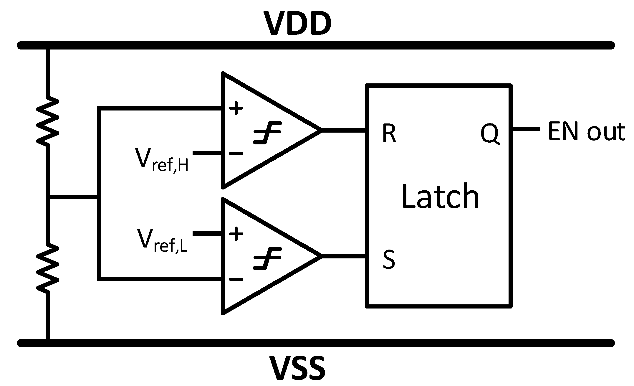
As shown in Figure 3, burst mode can be implemented with a supply capacitor and special burst-mode logic. Ideally, the power converter has an enable pin that allows the burst controller to shut down the converter. As shown in Figure 4 a simple burst controller can be implemented with two resistors, two voltage references (band gap or LDO), two comparators, and an SR latch. These components can all be easily integrated into the power converter’s controller. The resistor divider scales the voltage on the supply capacitor, which is then compared to a high and low reference. If the scaled voltage falls below the low reference, the latch is set, and the converter is enabled. Once the scaled voltage rises above the high reference, the latch is reset, and the converter is disabled.
Burst mode’s primary drawback is the output voltage ripple that results from draining and recharging the supply capacitor. The magnitude of ripple depends on the voltage references and the supply capacitor. In some cases, the ripple introduces audio-frequency noise, which can be problematic in certain analog applications. Nonetheless, many electronics can tolerate a small voltage ripple, particularly in standby mode. Another minor drawback is in the resistive losses from charging and discharging the supply capacitor.

2.2. Experimental Results

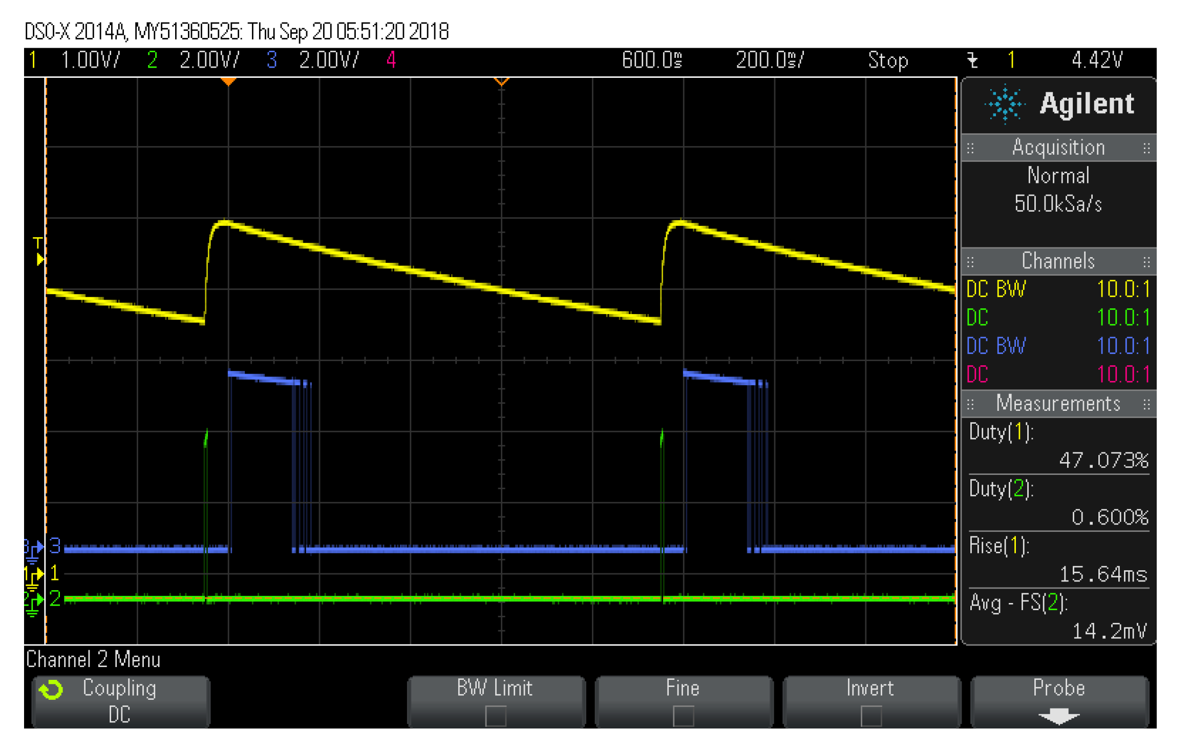
The savings with burst mode was measured in prototypes that follow the schematics of Figure 3 and Figure 4, and verified by the oscilloscope traces in Figure 5. The burst period in these experiments ranged from 0.25 to 2.25 s, which is considerably longer than found in typical products. These prototypes add burst mode functionality in two DC/DC converters: the 2 W Delta PG02S2405A and the 25 W Murata OKX-T/5-D12N-C, both of which have an enable (EN) pin and a five-volt output. The burst mode controller is comprised of a TPS78001DDCR LDO (low drop-out) reference, MCP6542 comparator, CD4043BE latch (output requires inversion), and two 10 mF 10 V electrolytic supply capacitors. These components all have an ultra-low quiescent current of 500 nA, 600 nA, and 100 nA, respectively. Finally, the LDO output and resistor divider are stabilized with 33 nF and 3.3 nF capacitors, respectively.
The experiment compares burst mode and normal operation for each converter. It simulates standby consumption by loading the converter with 470 Ω, 4.7 kΩ, and 47 kΩ resistors (RL). In burst mode, the average output power is estimated based on the burst period T, the high voltage V1, and the low voltage V2:
P a v g = 1 R L T 0 T ( V 1 e t / τ ) 2 d t
τ = T l n ( V 1 ) l n ( V 2 )
As shown in Table 1, Table 2, Table 3 and Table 4, burst mode allows for considerable savings at light loads. Burst mode’s savings are mainly a result of eliminating the no-load input power, which is 89 mW and 471 mW for the PG02S2405A and OKX-T/5-D12N-C, respectively. These savings become less significant with heavier loads.
This work first recommends that more converters be designed with a burst-mode capability. In particular, application-specific wall adapters should always consider burst mode, depending on the tolerable voltage ripple for the application in standby mode. Second, this work recommends that packaged converters without burst mode contain an enable pin so that burst mode can be added as the application allows. Finally, this work recommends that a separate burst-mode logic chip be designed for such converters.

3. Sleep Transistors

3.1. General Background

The sleep transistor is a solid-state power switch that can disconnect the main device or module from power, and is crucial in any standby-killer solution. Solid-state switches are often preferable over mechanical relays in low-power electronics due to speed and life span. Sleep transistors have traditionally been used for selectively deactivating modules in digital ICs [15,16,17,18,19]. In particular, low-voltage digital ICs greatly benefit from sleep transistors because they avoid the excessive sub-threshold leakage present in low-voltage transistors. Sleep transistors with high gate thresholds have been applied in these modules to block the leakage current.
There are two main types of sleep transistor configurations: the footer switch and the header switch. Either configuration can also be cascoded (stacked transistors) to allow for a greater blocking voltage. Although they can only block DC, future work can extend these solid-state solutions to AC through the use of triacs. Sleep transistors can have drawbacks such as on-state resistance and leakage current, both of which are mitigated by proper metal oxide semiconductor field effect transistor (MOSFET) selection.

3.2. Footer Switch

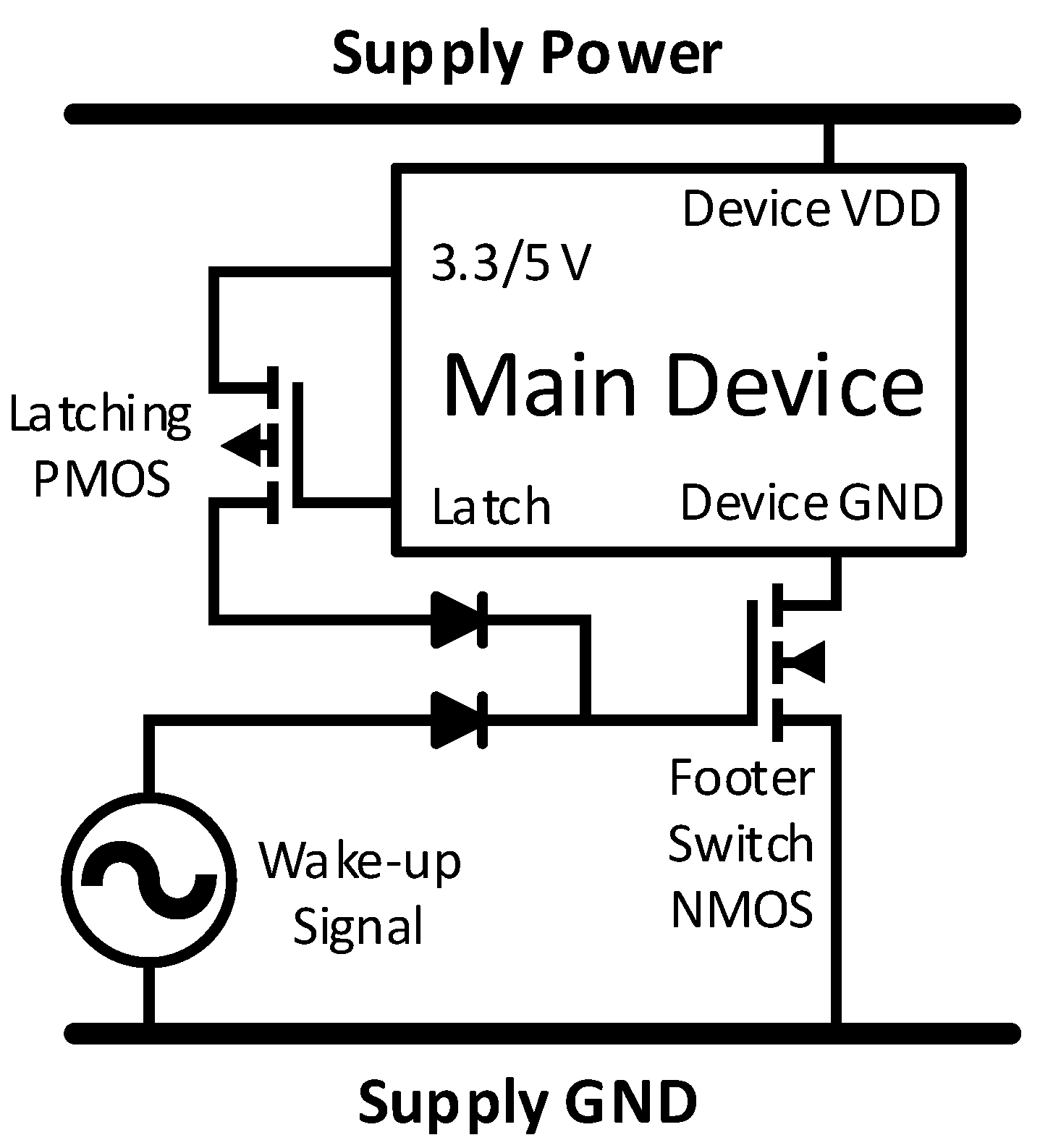
The footer switch, shown in Figure 6, is an N-type MOSFET that connects the ground of the main device to the ground of the power supply. The simplicity and reliability of these switches have made them become a recent favorite in standby reduction techniques. The footer switch allows the main device to completely shut down, resulting in zero standby power consumption. However, the device can only turn on if a sufficient wake-up drive signal is applied at the footer-switch gate. Once awake, the device must also latch the gate high so as to remain powered. After completing its operation, the device can return to a zero-standby mode by unlatching the footer gate. Section 4 and Section 5 show methods for providing this wake-up signal.

3.3. Header Switch

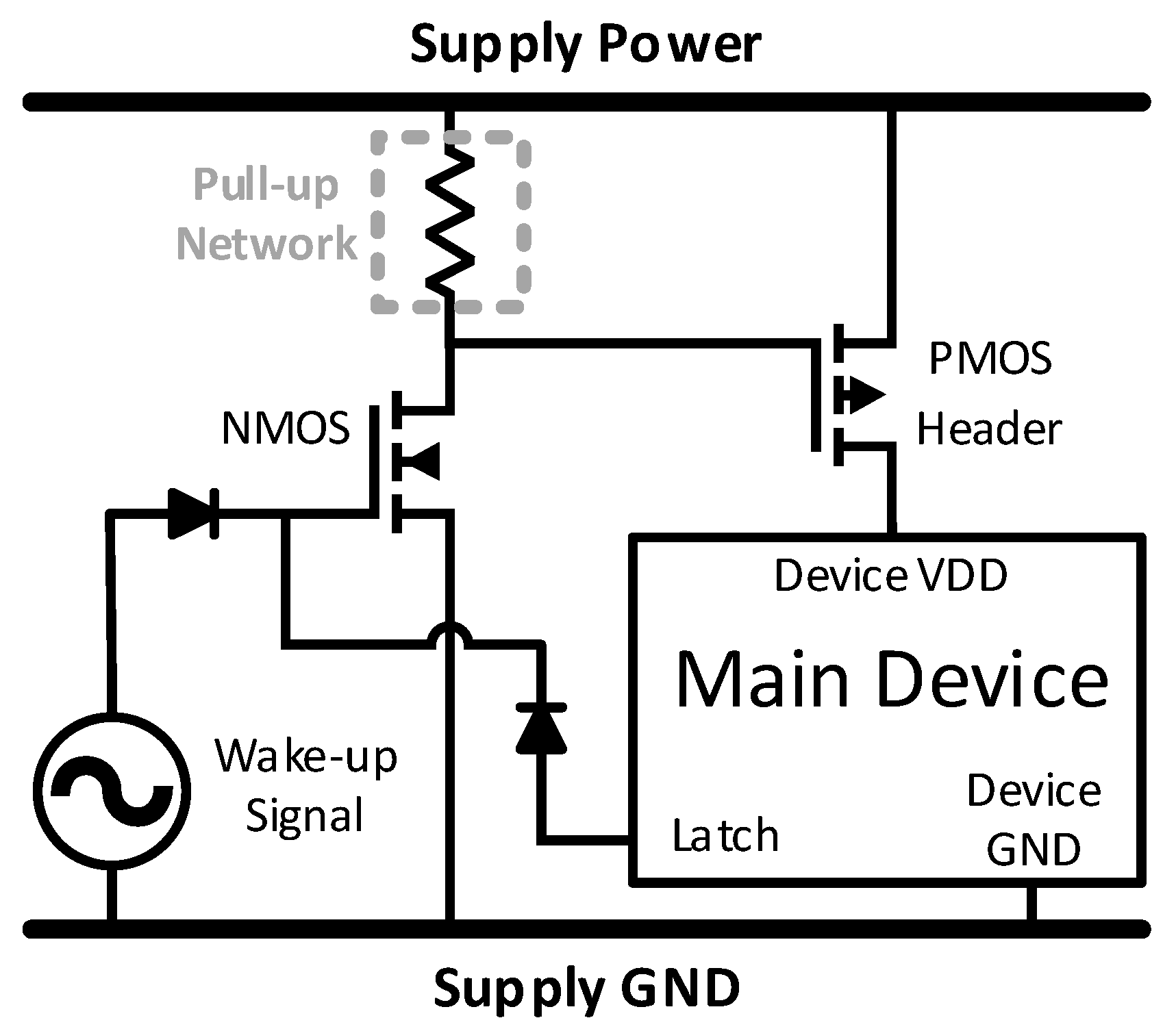
The header switch is a high-side PMOS (p-type MOSFET) sleep transistor, shown in Figure 7. This configuration is useful in applications that require a fixed ground reference between the device and wake-up signal. In this topology, the wake-up signal activates a low-power NMOS (n-type MOSFET), which then activates the gate of the header-switch PMOS through a pull-up resistor [20].

3.4. Cascoded Header Switch

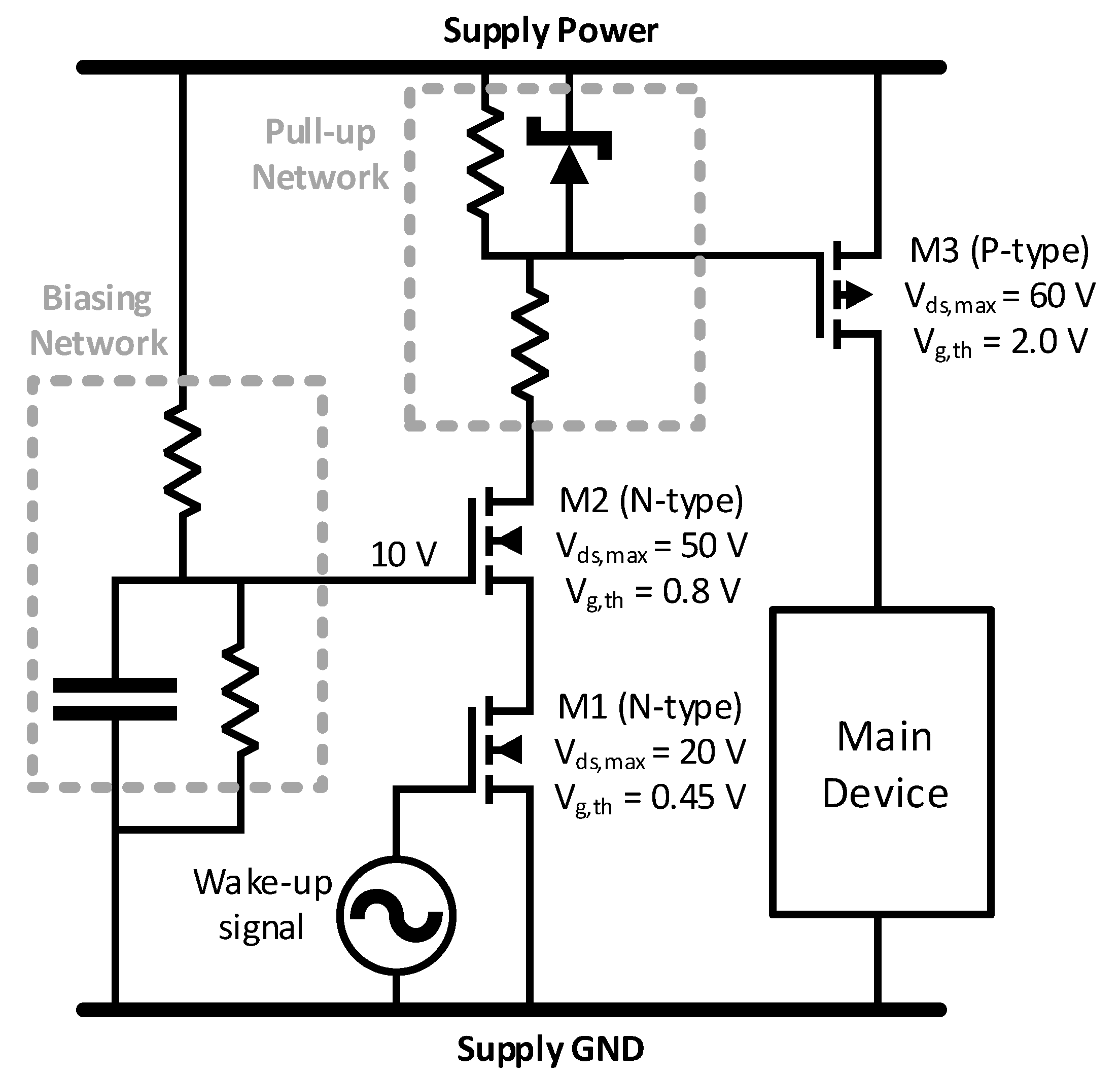
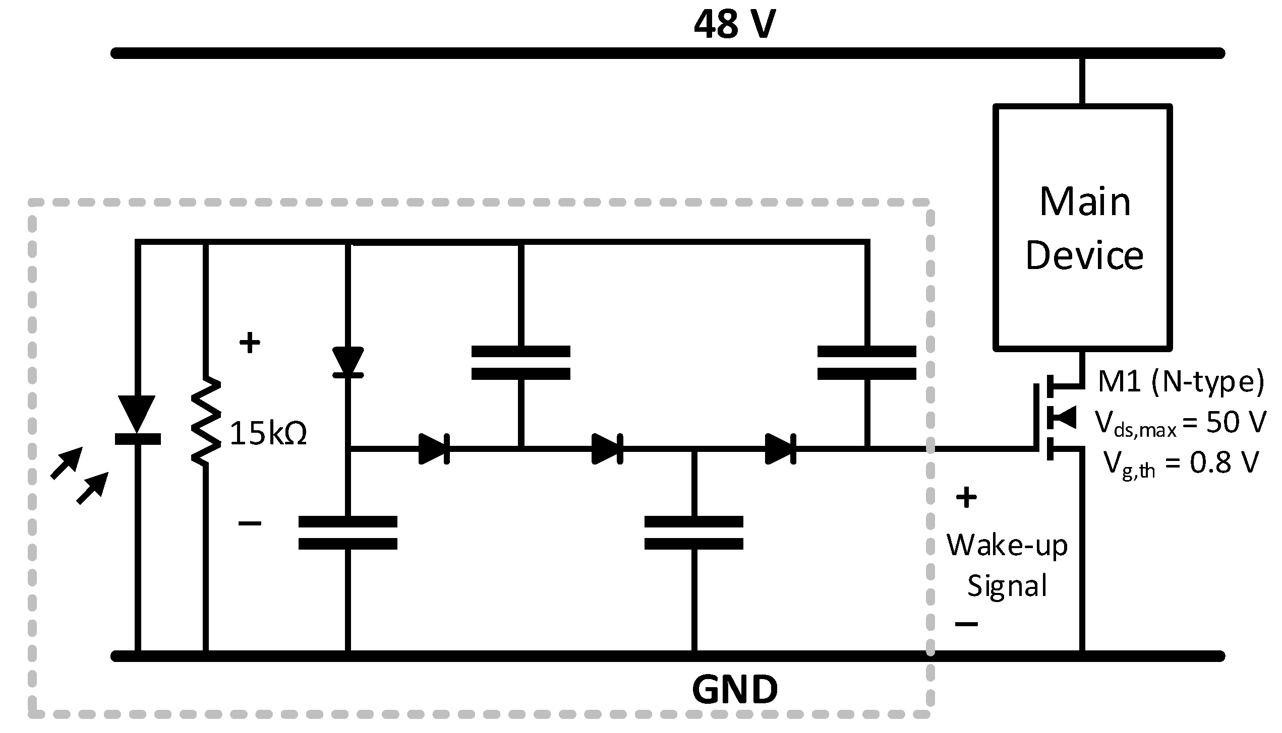
The cascoded header is a variant of the header switch that is ideal for a high supply voltage, such as the 170 V output of a bridge rectifier. It was developed in this work explicitly for the laser-based zero standby solution in Section 4 [30]. As shown in Figure 8, the cascoded header uses two NMOS transistors to activate the header switch gate. The top NMOS (M2) is a high-voltage device, and the bottom NMOS (M1) is a low-voltage device with a low gate-threshold voltage. This combination of devices allows for a low gate threshold, while simultaneously being able to withstand a high supply voltage. The cascoded header may also be useful for applying MEMS-based solutions in plug loads.

4. Optical Wake-Up Signal

4.1. Infrared Wake-Up Signal

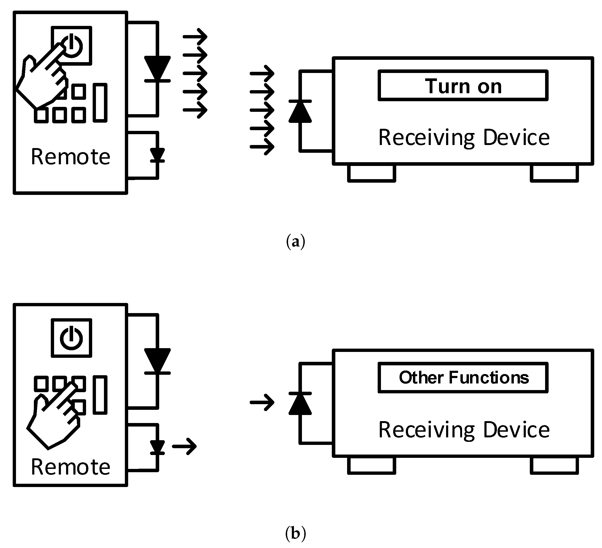
Several papers propose a sleep transistor standby-killer topology with a high-power IR wake-up signal, shown in Figure 9. Yamawaki and Serikawa described a method for driving the footer switch using IR energy harvested from a photodiode [21]. Although the intended application was for set-top boxes, this method can extend to any device that requires line of sight activation, such as lights, ceiling fans, and window coverings. The main drawback of IR LEDs is in their wide-beam nature, which disperses much of the transmission power. Yamawaki and Serikawa found their maximum transmission range to be 3 m. Other past works in optical zero-standby solutions yield a similar range of 2–6 m [22,23,24,25,26,29].
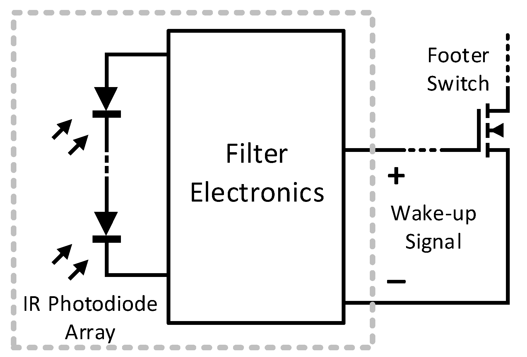
This paper presents an IR LED zero-standby prototype based on the architecture developed by Yamawaki and Serikawa [21]. As shown in Figure 10, the receiver contains a photodiode array that harvests a high-power IR transmission at 38 kHz. The array generates an output voltage relative to the transmission strength and the number of photodiodes illuminated. To activate a typical mid-power 50 V footer switch, the photodiode array usually needs to generate about 0.5–0.8 V. In this prototype, the array output is passed through a 38 kHz band-pass filter and rectified to provide an appropriate wake-up signal at the gate of a footer switch.
The prototype, shown in Figure 11, was developed to test the practicality of the IR-based zero standby method. The transmitter provides 14 W pulses to four IR LEDs, and the receiver contains an array of twelve photodiodes. Although the prototype demonstrates zero standby power, it has several practical shortcomings. First, the prototype’s reliable transmission range is a mere 1 m. Second, the IR LEDs must be perfectly aligned with the photodiode array, which is difficult to achieve because IR emissions are invisible. Finally, the required transmission power approaches a level that becomes questionable for eye safety.

4.2. Laser Wake-Up Signal

A laser-based zero-standby supply was developed to address the IR method’s shortcomings [30]. Visible-light lasers are easy to aim and have a narrow beam that significantly increases the activation range. Both optical methods use a receiver that harvests optical energy to drive the gate of a footer switch, but they differ in wake-up circuitry. The laser’s receiver only needs a single photodiode to function, although an array is still helpful for increasing the effective area over which the laser can be aimed. It also requires a special front-end circuit in order to drive the gate of the sleep transistor.
The need for a front-end circuit is related to the safety concerns surrounding high-power lasers. Any laser with an instantaneous power greater than 5 mW (laser class IIIa) is subject to strict regulations. As such, the transmitter is limited to operate below 5 mW, which is similar to a common, off-the-shelf laser pointer. This presents a challenge since most affordable photodiodes cannot generate the requisite gate-drive voltage from 5 mW. For example, a SFH206K photodiode can only generate up to 0.5 V, whereas a typical 50 V NMOS has a gate threshold voltage of 0.8 V. Two front-end circuit topologies are developed to address this challenge.
The first topology is the cascoded header switch in Figure 7, which allows the bottom NMOS to have an extremely low gate threshold voltage. The gate threshold of the Si3460DV NMOS is 0.45 V, which can be activated by the 0.5 V photodiode wake signal. Nonetheless, this topology leaves little margin for error, and an angled or diffracted illumination may fail to activate the device.
The second topology utilizes a charge pump circuit to step-up the output voltage of the photodiode. The Dickson charge pump, shown in Figure 12, is convenient in harvesting applications since it is self-powered. In addition, the photodiode voltage can be multiplied over several stages, allowing the voltage at the footer-switch gate to be well above its gate threshold. Since the charge pump requires an AC input, the laser is pulsed at 1 kHz. The main drawback is in the Schottky diode drop of 0.2 V, which causes each stage to be less efficient, ultimately increasing the overall hardware cost.
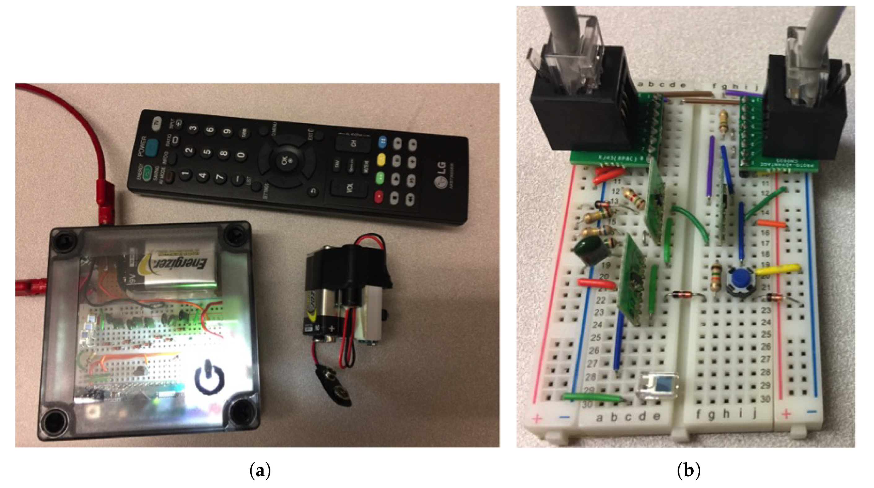
The laser-based prototypes, shown in Figure 13, are built from inexpensive off-the-shelf components. Unlike previous works, these prototypes are explicitly designed for use in plug-load applications. The estimated standby consumption of the charge-pump prototype in Figure 13a is 10 µW. The cascoded header prototype in Figure 13b is estimated to consume 250 µW, which is mostly in the biasing network. The charge-pump prototype in Figure 13a experimentally demonstrates successful wake-up at a range of 25 m. Overall, the laser-based method has potential as a long-range, low-power alternative to the IR-based zero-standby solutions.
The circuits discussed in this section may also prove useful in fiber optics applications. Fiber communication transmits at a similar power level and uses a wave-guide to focus the light. Further research is required to verify the applications of any fiber-based zero-standby solution.

5. Wake-Up Radio

An RF-based wake-up signal is appealing due to the proliferation of wirelessly-connected technologies that contain a built-in transceiver and antenna. Various ideas have been proposed for ambient or broadcasted RF harvesting [78,79]. However, in most cases, the amount of transmission power required for pure RF harvesting makes it difficult to justify its use in plug-load applications.
For plug-loads, the wake-up radio (WuR) is a more appealing method. WuRs are a family of ultra-low-power receivers that are designed solely to wake the main device from sleep mode [41,42]. Modern and future trends in electronics suggest that many devices and appliances will be wirelessly IoT-connected. Even set-top boxes and remotes have begun to transition from IR to WiFi-based communication. At present, most research in WuRs is applied to prolonging battery life in remote IoT applications. Some works, such as Umeda and Otaka, propose the application of WuRs in plug loads [43]. This work demonstrates another means for deploying the WuR in plug loads.
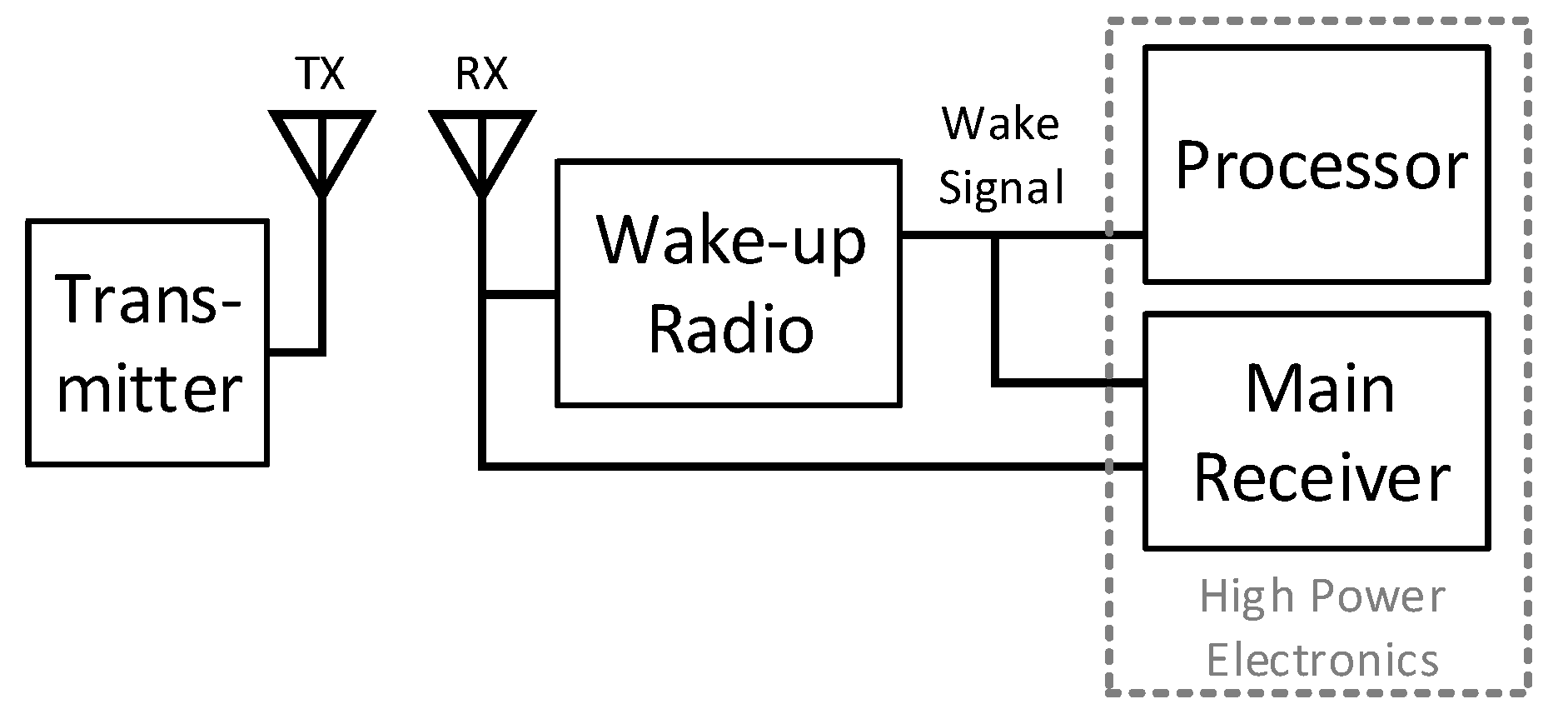
As shown in Figure 14, WuRs are electrically separate from the device’s primary high-power transceiver, but both devices share the same antenna. They can be programmed to be individually addressable, thus allowing the wake-up broadcast to wake individual devices. Although the WuR does not strictly allow for zero standby consumption, its microwatt consumption is practically negligible.
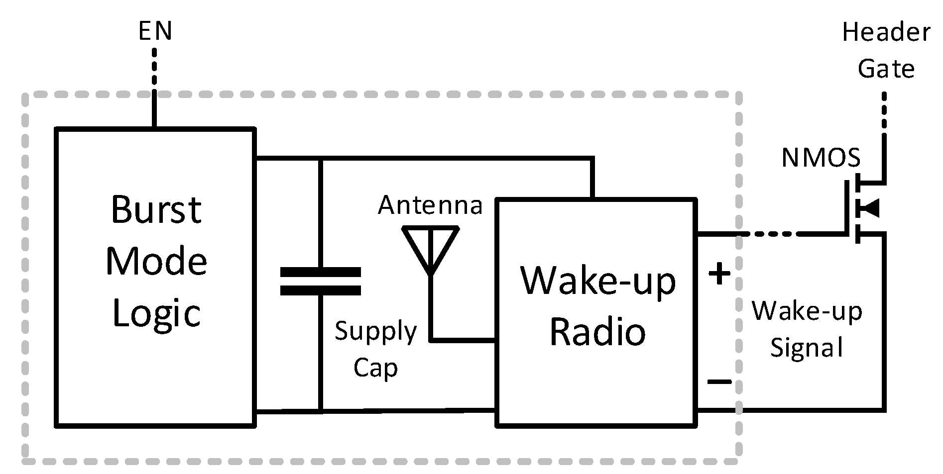
As shown in Figure 15, plug-load WuRs can toggle a footer switch similar to the IR- and laser-based methods. Unlike these methods, the WuR requires a constant current of several microamps. While the wall adapter can provide this current, most converters do not operate efficiently at low power. In addition, the wakeup radio might operate at a lower voltage compared to the rest of the device electronics. As such, this work recommends powering the WuR using the burst-mode techniques discussed in Section 2. With these modifications, the WuR is an effective way to reduce standby power in wirelessly-connected plug loads.
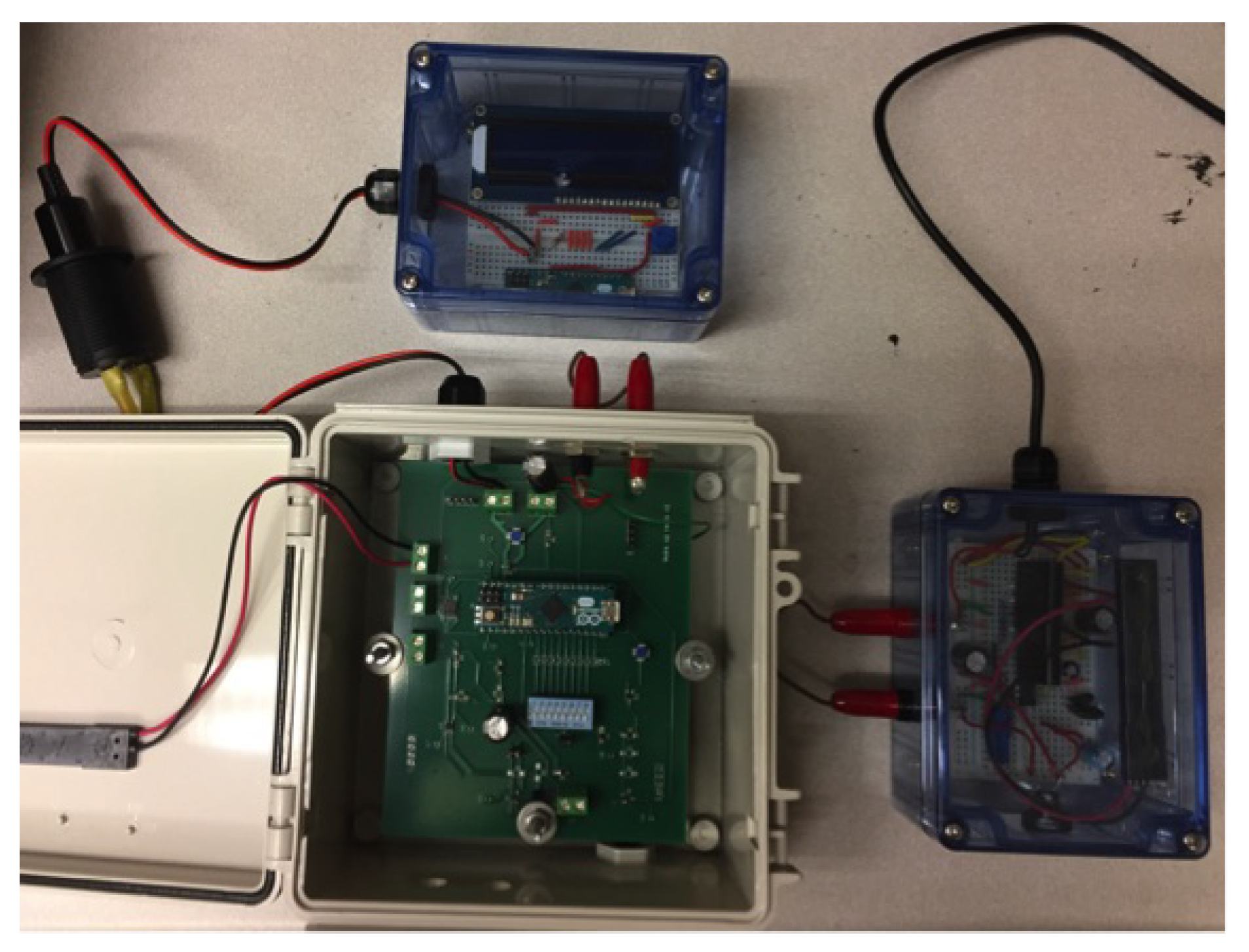
A prototype for the method in Figure 15 was developed using the AS3932 WuR chip. Unlike previous works, this prototype is designed for plug-loads, and can function at high voltage through the combination of burst mode and a high-voltage header switch. Its standby consumption is estimated to be 30 µW. The prototype, shown in Figure 16, uses near-field magnetic coupling at 125 kHz to turn the device on from across the room. However, its range is relatively limited at 3 m, and is heavily affected by metal shielding. Nonetheless, Gamm et al. and Oller et al. both demonstrated the use of various RF techniques that allow the AS3932 to wake at 50 m with an 868 MHz signal [44,45]. With proper design of the antenna, board, and RF downconverter, the prototype in this work can be upgraded for a similar frequency and range.
This work recommends the WuR for all wirelessly-connected products, both battery-powered and plug loads. Nonetheless, addressing protocols must be standardized before WuRs can become prevalent. One possibility is for routers to become a centralized broadcasting unit. Remotes could request the router to broadcast a wake signal addressed to the remote’s specific target. Alternatively, IoT devices with occasional periodic functions could request the router to schedule a periodic wake-up. This work also recommends integrating burst-mode logic into commercial WuR products. Burst mode would provide a convenient and efficient means of powering the WuR, and help expand its application in many types of products.

6. Conclusions

Improvements to power supplies have drastically reduced standby consumption over the last twenty years. However, the need for standby power reduction persists due to the increasing population of devices with standby modes. Since modern electronics are very diverse in application and requirements, this work suggests a portfolio of solutions to tackle standby consumption. Several such solutions are presented and prototyped. The first demonstrates the value of burst mode for lightly-loaded converters. The second uses IR energy harvesting to activate a footer switch and wake the device. The third, instead, harvests visible light energy from a laser pointer. The fourth solution uses a wake-up radio to activate a header switch. As IoT technology transitions loads to become small and numerous, intensive standby reduction will be crucial for energy-efficient products.
This work demonstrates zero or near-zero standby power as being technically feasible in several families of products. These solutions have both advantages and drawbacks and will require technical improvements and reductions in cost before they can be commercialized. In addition, the portfolio of solutions will need to be broadened before standby power use can be confidently and economically eliminated.

Author Contributions

The authors made the following contributions: conceptualization, D.G. and A.M.; methodology, D.G. and R.H.; software, D.G. and R.L.; validation, D.G., R.L., and R.H.; formal analysis, D.G.; investigation, D.G. and A.M.; resources, A.M.; data curation, D.G. and R.L.; writing—original draft preparation, D.G.; writing—review and editing, A.M., R.L., and R.H.; visualization, D.G.; supervision, A.M.; project administration, A.M.; funding acquisition, A.M.

Acknowledgments

This work was supported by the California Energy Commissions EPIC Project EPC-15-024. The authors would like to thank Alan Meier, Leo Rainer, Bruce Nordman, and Seth Sanders for their technical advice and support. Special thanks to the reviewers and editors.

Conflicts of Interest

The authors have no conflict of interest. The funders provided guidelines and participated in a technical advisory board. Other than this, the funders had no other role in the design of the study; in the collection, analyses, or interpretation of data; in the writing of the manuscript, or in the decision to publish the results.

References

  1. IEA. Things that Go Blip in the Night: Standby Power and How to Limit It; Technical Report; International Energy Agency: Paris, France, 2001. [Google Scholar]
  2. Urban, B.; Tiefenbeck, V.; Roth, K. Energy Consumption of Consumer Electronics in US Homes in 2010; Fraunhofer Center for Sustainable Energy Systems: Boston, MA, USA, 2011. [Google Scholar]
  3. Delforge, P.; Schmidt, L.; Schmidt, S. Home Idle Load: Devices Wasting Huge Amounts of Electricity When Not in Active Use; NRDC Issue Paper IP:15-03-A; Natural Resources Defense Council: San Francisco, CA, USA, 2015. [Google Scholar]
  4. Lu, T.K.; Yeh, C.T.; Chang, W.C. Measuring the use of residential standby power in Taiwan. Energy Build. 2011, 43, 3539–3547. [Google Scholar] [CrossRef]
  5. De Almeida, A.T.; Patrao, C.; Riviere, P.; Da Silva, D.; Schlomann, B.; Gigli, M.; Harrison, B. Standby and off-mode power demand of new appliances in the market. In Proceedings of the 6th International Conference on Energy Efficiency in Domestic Appliances and Lighting (EEDAL’11), Copenhague, Danemark, 24–26 May 2011; p. 12. [Google Scholar]
  6. Clement, K.; Pardon, I.; Driesen, J. Standby power consumption in Belgium. In Proceedings of the 9th International Conference on Electrical Power Quality and Utilisation (EPQU 2007), Piscataway, NJ, USA, 9–11 October 2007; pp. 1–4. [Google Scholar]
  7. Sahin, M.C.; Aydinalp Koksal, M. Standby electricity consumption and saving potentials of Turkish households. Appl. Energy 2014, 114, 531–538. [Google Scholar] [CrossRef]
  8. Ahmadi-Karvigh, S.; Ghahramani, A.; Becerik-Gerber, B.; Soibelman, L. Real-time activity recognition for energy efficiency in buildings. Appl. Energy 2018, 211, 146–160. [Google Scholar] [CrossRef]
  9. IEA. More Data, Less Energy: Making Network Standby More Efficient in Billions of Connected Devices; Technical Report; IEA: Paris, France, 2014. [Google Scholar]
  10. Comstock, O.; Jarzomski, K. Consumption and saturation trends of residential miscellaneous end-use loads. In Proceedings of the 2012 ACEEE Summer Study Energy Efficiency Buildings, Pacific Grove, CA, USA, 12–17 August 2012. [Google Scholar]
  11. IEC 62301:2011: Household Electrical Appliances—Measurement of Standby Power; Technical Report; International Electrotechnical Commission Standard: Geneva, Switzerland, 2011.
  12. Bourassa, N.L.; Rainer, L.; Mai, J.; Curtin, C. Final Standardized Test Bed Specification and Findings Report (Task 5); Technical Report; Lawrence Berkeley National Laboratory: Berkeley, CA, USA, 2018.
  13. Ellis, M.; Siderius, H.P.; Lane, K. Closing the Gap towards Net Zero Energy Appliances; ECEEE 2015 Summer Study Proceedings; European Council for an Energy-Efficient Economy: Hyères, France, 2015. [Google Scholar]
  14. Meier, A.; Siderius, H.P. Should the Next Standby Power Target Be 0-Watt? European Council for an Energy-Efficient Economy: Hyeres, France, 2017. [Google Scholar]
  15. Jiang, H.; Marek-Sadowska, M.; Nassif, S.R. Benefits and costs of power-gating technique. In Proceedings of the 2005 IEEE International Conference on Computer Design: VLSI in Computers and Processors, San Jose, CA, USA, 2–5 October 2005; pp. 559–566. [Google Scholar]
  16. Shi, K.; Howard, D. Challenges in sleep transistor design and implementation in low-power designs. In Proceedings of the 43rd Annual Design Automation Conference, San Francisco, CA, USA, 24–28 July 2006; pp. 113–116. [Google Scholar]
  17. Long, C.; He, L. Distributed sleep transistor network for power reduction. IEEE Trans. Very Large Scale Integr. VLSI Syst. 2004, 12, 937–946. [Google Scholar] [CrossRef] [Green Version]
  18. Fallah, F.; Pedram, M. Standby and active leakage current control and minimization in CMOS VLSI circuits. IEICE Trans. Electron. 2005, 88, 509–519. [Google Scholar] [CrossRef]
  19. Fukuoka, K.; Maeda, N.; Nii, K.; Fujigaya, M.; Sakamoto, N.; Koike, T.; Irita, T.; Wakahara, K.; Matsuyama, T.; Hasegawa, K.; et al. Power-Management Features of R-Mobile U2, an Integrated Application Processor and Baseband Processor. IEEE Micro 2013, 33, 26–36. [Google Scholar] [CrossRef]
  20. Chao, B.; Harrison, L. Re-Designing Normally-on Load Switches with Zero-Power Mosfets Reduces Power Consumption; Advanced Linear Devices: Sunnyvale, CA, USA, 2008. [Google Scholar]
  21. Yamawaki, A.; Serikawa, S. Power supply circuit with zero standby power consumption on infrared remote controlled product by using energy harvesting. In Proceeding of the International MultiConference of Engineers and Computer Scientists, Hong Kong, China, 18–20 March 2015; Volume 2, p. 00002. [Google Scholar]
  22. Park, K.H.; Yi, K.H. Cost-effective power system with an electronic double layer capacitor for reducing the standby power consumption of consumer electronic devices. J. Power Electron. 2013, 13, 362–368. [Google Scholar] [CrossRef]
  23. Koidea, D.; Yoshikawaa, K.; Yamawakia, A. Remote power strip with zero standby power controllable from every direction. In Proceeding of the ICISIP 2015: The 3rd IIAE International Conference on Intelligent Systems and Image Processing, Fukuoka, Japan, 2–5 September 2015. [Google Scholar]
  24. Reshma, A.R. Standby Power Reduction System. Int. J. Eng. Innov. Technol. 2014, 4, 139–142. [Google Scholar]
  25. Rosa, R.L.; Aiello, N.; Zoppi, G. An Innovative System Capable to Turn on Any Turned off electrical appliance by means of an efficient optical energy transfer. In Proceedings of the International Exhibition and Conference for Power Electronics, Intelligent Motion, Renewable Energy and Energy Management, Nuremberg, Germany, 20–22 May 2014; pp. 1–8. [Google Scholar]
  26. Utsunomiya, F.; Tanaka, A.; Douseki, T. A self-powered photosensor switch detects only rising edge of infrared-light pulse for wireless zero-standby-power wake-up receiver. In Proceedings of the 2013 IEEE SENSER, Baltimore, MD, USA, 3–6 November 2013; pp. 1–4. [Google Scholar] [CrossRef]
  27. Rajaram, V.; Qian, Z.; Kang, S.; Cassella, C.; McGruer, N.E.; Rinaldi, M. Microelectromechanical detector of infrared spectral signatures with near-zero standby power consumption. In Proceeding of the 19th International Conference on Solid-State Sensors, Actuators and Microsystems (TRANSDUCERS), Kaohsiung, Taiwan, 18–22 June 2017; pp. 846–849. [Google Scholar] [CrossRef]
  28. Qian, Z.; Kang, S.; Rajaram, V.; Cassella, C.; McGruer, N.E.; Rinaldi, M. Zero-power infrared digitizers based on plasmonically enhanced micromechanical photoswitches. Nat. Nanotechnol. 2017, 12, 969–973. [Google Scholar] [CrossRef]
  29. Kang, S.; Park, K.; Shin, S.; Chang, K.; Kim, H. Zero Standby Power Remote Control System Using Light Power Transmission. IEEE Trans. Consum. Electron. 2011, 57, 1622–1627. [Google Scholar] [CrossRef]
  30. Gerber, D.L.; Meier, A.; Hosbach, R.; Liou, R. Zero Standby Solutions with Optical Energy Harvesting from a Laser Pointer. Electronics 2018, 7, 292. [Google Scholar] [CrossRef]
  31. Tsai, C.H.; Bai, Y.W.; Lin, M.B.; Jhang, R.J.R.; Chung, C.Y. Reduce the standby power consumption of a microwave oven. IEEE Trans. Consum. Electron. 2013, 59, 54–61. [Google Scholar] [CrossRef]
  32. Shibasaki, K.; Kono, S.; Yamawaki, A. An Architecture of Energy Efficient Restroom by Making Zero Standby Power. In Proceedings of the 5th IIAE International Conference on Industrial Application Engineering, Kitakyushu, Japan, 27–31 March 2017; pp. 323–326. [Google Scholar]
  33. Yamawaki, A.; Serikawa, S. Applying sensor node with zero standby power to door monitor. In Proceedings of the International MultiConference of Engineers and Computer Scientists 2016, Hong Kong, China, 16–18 March 2016; pp. 2183–2187. [Google Scholar]
  34. Takaichi, Y.; Koide, D.; Yamawaki, A. Wake-up time Measurement of Wireless Sensor Node with Zero Standby-power. In Proceedings of the 4th IIAE International Conference on Intelligent Systems and Image Processing 2016, Kyoto, Japan, 8–12 September 2016; pp. 225–228. [Google Scholar] [CrossRef]
  35. Chalko, T. A fridge that takes only 0.1 kWh a day? Renew (Australia) 2005, 90, 36–40. [Google Scholar]
  36. Kuwatani, T.; Takaichi, Y.; Yamawaki, A. A Fire Alarm Sensor Node with Long Battery Life by Zero Standby Power Consumption. In Proceedings of the 5th IIAE International Conference on Industrial Application Engineering, Kitakyushu, Japan, 27–31 March 2017; pp. 327–330. [Google Scholar] [CrossRef]
  37. Zhang, L.; Jiang, H.; Sun, X.; Zhang, C.; Wang, Z. A passive RF receiving and power switch ASIC for remote power control with zero stand-by power. In Proceedings of the IEEE Asian Solid-State Circuits Conference, Fukuoka, Japan, 3–5 November 2008; pp. 109–112. [Google Scholar]
  38. Chen, L.; Wang, Z.; Jia, C.; Li, F.; Hao, W.; Xiao, B.; Zhang, C.; Wang, Z. A RF remote-control transceiver with zero-standby power based on RFID technology. Electronics 2010, 243–246. [Google Scholar]
  39. Siwamogsatham, S.; Rattanawan, P.; Kitjaroen, M.; Songtung, P.; Pongpaibool, P.; Navanugraha, K. Smartly saving energy with a zero power consumption standby system. In Proceedings of the 2011 Proceedings of PICMET ’11: Technology Management in the Energy Smart World (PICMET), Portland, OR, USA, 31 July–4 August 2011; pp. 1–4. [Google Scholar]
  40. Mozar, S.; Funabiki, N. Switching System, a Zero Power Standby Solution. Int. J. Eng. Res. Sci. 2017, 3, 2395–6992. [Google Scholar]
  41. Demirkol, I.; Ersoy, C.; Onur, E. Wake-up receivers for wireless sensor networks: benefits and challenges. IEEE Wirel. Commun. 2009, 16, 88–96. [Google Scholar] [CrossRef]
  42. Magno, M.; Marinkovic, S.; Srbinovski, B.; Popovici, E.M. Wake-up radio receiver based power minimization techniques for wireless sensor networks: A review. Microelectron. J. 2014, 45, 1627–1633. [Google Scholar] [CrossRef]
  43. Umeda, T.; Otaka, S. ECO chip: Energy consumption zeroize chip with a 953MHz high-sensitivity radio wave detector for standby mode applications. In Proceedings of the Custom Integrated Circuits Conference, San Jose, CA, USA, 16–19 September 2007; pp. 663–666. [Google Scholar]
  44. Gamm, G.U.; Sippel, M.; Kostic, M.; Reindl, L.M. Low power wake-up receiver for wireless sensor nodes. In Proceedings of the 2010 Sixth International Conference on Intelligent Sensors, Sensor Networks and Information Processing (ISSNIP), Brisbane, Australia, 7–10 December 2010; pp. 121–126. [Google Scholar]
  45. Oller, J.; Demirkol, I.; Casademont, J.; Paradells, J.; Gamm, G.U.; Reindl, L. Performance evaluation and comparative analysis of subcarrier modulation wake-up radio systems for energy-efficient wireless sensor networks. Sensors 2013, 14, 22–51. [Google Scholar] [CrossRef]
  46. Jiang, H.; Wang, P.P.; Gao, L.; Sen, P.; Kim, Y.; Rebeiz, G.M.; Hall, D.A.; Mercier, P.P. 24.5 A 4.5 nW wake-up radio with −69 dBm sensitivity. In Proceedings of the 2017 IEEE International Solid-State Circuits Conference (ISSCC), San Francisco, CA, USA, 5–9 February 2017; pp. 416–417. [Google Scholar] [CrossRef]
  47. Wang, P.P.; Jiang, H.; Gao, L.; Sen, P.; Kim, Y.; Rebeiz, G.M.; Mercier, P.P.; Hall, D.A. A Near-Zero-Power Wake-Up Receiver Achieving −69 dBm Sensitivity. IEEE J. Solid-State Circuits 2018, 53, 1640–1652. [Google Scholar] [CrossRef]
  48. Moody, J.; Bassirian, P.; Roy, A.; Liu, N.; Pancrazio, S.; Barker, N.S.; Calhoun, B.H.; Bowers, S.M. A −76 dBm 7.4 nW wakeup radio with automatic offset compensation. In Proceedings of the 2018 IEEE International Solid-State Circuits Conference (ISSCC), San Francisco, CA, USA, 11–15 February 2018; pp. 452–454. [Google Scholar] [CrossRef]
  49. Bassirian, P.; Moody, J.; Lu, R.; Gao, A.; Manzaneque, T.; Roy, A.; Barker, N.S.; Calhoun, B.H.; Gong, S.; Bowers, S.M. Nanowatt-Level Wakeup Receiver Front Ends Using MEMS Resonators for Impedance Transformation. IEEE Trans. Microwave Theory Tech. 2019, 67, 1615–1627. [Google Scholar] [CrossRef]
  50. Tsai, C.H.; Bai, Y.W.; Lin, M.B.; Jhang, R.R.; Lin, Y.W. Design and implementation of a PIR luminaire with zero standby power using a photovoltaic array in enough daylight. IEEE Trans. Consum. Electron. 2013, 59, 499–506. [Google Scholar] [CrossRef]
  51. Tsai, C.H.; Bai, Y.W.; Chu, C.A.; Chung, C.Y.; Lin, M.B. Design and implementation of a socket with zero standby power using a photovoltaic array. IEEE Trans. Consum. Electron. 2010, 56, 2686–2693. [Google Scholar] [CrossRef]
  52. Tsai, C.H.; Bai, Y.W.; Cheng, L.C.; Lin, K.S.; Jhang, R.J.R.; Lin, M.B. Reducing the standby power consumption of a pc monitor. In Proceedings of the 1st IEEE Global Conference on Consumer Electronics, Las Vegas, NV, USA, 11 September 2012; pp. 520–524. [Google Scholar]
  53. Tsai, C.H.; Bai, Y.W.; Chen, P.C.; Jhang, R.J.R.; Lin, M.B. Reduction of the standby power consumption of an automatic door system. In Proceedings of the 2016 IEEE International Conference on Consumer Electronics (ICCE), Las Vegas, NV, USA, 9–11 Janurary 2016; pp. 583–584. [Google Scholar]
  54. Golchin, P.; Tosato, P.; Brunelli, D. Design optimization of zero power wake-up receiver in Power line communication. In Proceedings of the 2016 International Symposium on Power Electronics, Electrical Drives, Automation and Motion (SPEEDAM), Anacapri, Italy, 22–24 June 2016; pp. 564–569. [Google Scholar] [CrossRef]
  55. Golchin, P.; Tosato, P.; Brunelli, D. Zero-energy wake up for power line communications in smart cities. In Proceedings of the 2016 IEEE International Smart Cities Conference (ISC2), Trento, Italy, 12–15 September 2016; pp. 1–6. [Google Scholar] [CrossRef]
  56. Mishra, N.; Chebrolu, K.; Raman, B.; Pathak, A. Wake-on-WLAN. In Proceedings of the 15th International Conference on World Wide Web, New York, NY, USA, 23–26 May 2006; pp. 761–769. [Google Scholar]
  57. Ricciardi, S.; Santos-Boada, G.; Careglio, D.; Palmieri, F.; Fiore, U. Evaluating energy savings in WoL-enabled networks of PCs. In Proceedings of the 2013 IEEE International Symposium on Industrial Electronics, Taipei, Taiwan, 28–31 May 2013; pp. 1–6. [Google Scholar] [CrossRef]
  58. Lieberman, P. White Paper: Wake on Lan Technology; Lieberman Software Corporation: Los Angeles, CA, USA, 2006. [Google Scholar]
  59. Olsson, R.H.; Bogoslovov, R.B.; Gordon, C. Event driven persistent sensing: Overcoming the energy and lifetime limitations in unattended wireless sensors. In Proceedings of the 2016 IEEE SENSORS, Orlando, FL, USA, 30 October–2 November 2016; pp. 1–3. [Google Scholar] [CrossRef]
  60. Jeong, S.; Chen, Y.; Jang, T.; Tsai, J.; Blaauw, D.; Kim, H.; Sylvester, D. 21.6 A 12nW always-on acoustic sensing and object recognition microsystem using frequency-domain feature extraction and SVM classification. In Proceedings of the 2017 IEEE International Solid-State Circuits Conference (ISSCC), San Francisco, CA, USA, 5–9 February 2017; pp. 362–363. [Google Scholar] [CrossRef]
  61. Banerjee, A.; Farhoudi, N.; Ghosh, C.; Mastrangelo, C.H.; Kim, H.; Broadbent, S.J.; Looper, R. Picowatt gas sensing and resistance switching in tunneling nano-gap electrodes. In Proceedings of the 2016 IEEE SENSORS, Orlando, FL, USA, 30 October–2 November 2016; pp. 1–3. [Google Scholar] [CrossRef]
  62. Lo, Y.K.; Yen, S.C.; Lin, C.Y. A high-efficiency AC-to-DC adaptor with a low standby power consumption. IEEE Trans. Ind. Electron. 2008, 55, 963–965. [Google Scholar] [CrossRef]
  63. Lee, K.; Sung, C.; Yoon, H.; Kang, B. Improvement of power-conversion efficiency at light-load using a variable-duty burst mode. In Proceedings of the Power and Energy Conference at Illinois (PECI), Urbana, IL, USA, 22–23 February 2013; pp. 142–146. [Google Scholar]
  64. Kim, B.C.; Park, K.B.; Moon, G.W. Sawtooth burst mode control with minimum peak current in stand-by operation of power supply. In Proceedings of the 2011 IEEE 8th International Conference on Power Electronics and ECCE Asia (ICPE & ECCE), Jeju, Korea, 30 May–3 June 2011; pp. 474–479. [Google Scholar]
  65. Choi, J.-H.; Huh, D.-Y.; Kim, Y.-S. The improved burst mode in the stand-by operation of power supply. APEC-04 2004, 1, 426–432. [Google Scholar]
  66. Kim, J.; Jung, E.S.; Lee, Y.T.; Ryu, W. An implementation of energy-saving set-top box. In Proceedings of the 2015 International Conference on Information and Communication Technology Convergence (ICTC), Jeju Island, Korea, 28–30 October 2015; pp. 793–796. [Google Scholar]
  67. Huang, T.; Bai, Y.W.; Chao, S.K. Reducing the system standby power of a personal computer. IET Comput. Digital Tech. 2015, 9, 248–258. [Google Scholar] [CrossRef] [Green Version]
  68. Agarwal, Y.; Hodges, S.; Chandra, R.; Scott, J.; Bahl, V.; Gupta, R. Somniloquy: Augmenting network interfaces to reduce PC energy usage. In Proceedings of the NSDI 2009: 6th USENIX Symposium on Networked Systems Design and Implementation, Boston, MA, USA, 22–24 Aprial 2009. [Google Scholar]
  69. Bai, Y.W.; Ku, Y.T. Automatic room light intensity detection and control using a microprocessor and light sensors. IEEE Trans. Consum. Electron. 2008, 54, 1173–1176. [Google Scholar] [CrossRef]
  70. Pompermayer, D.C.; Có, M.A.; Donadel, C.B. Design and implementation of a low-cost intelligent device to standby mode consumption reduction in already existing electrical equipment. IEEE Trans. Consum. Electron. 2017, 63, 145–152. [Google Scholar] [CrossRef]
  71. Byun, J.; Park, S.; Kang, B.; Hong, I.; Park, S. Design and implementation of an intelligent energy saving system based on standby power reduction for a future zero-energy home environment. IEEE Trans. Consum. Electron. 2013, 59, 507–514. [Google Scholar] [CrossRef]
  72. Heo, J.; Hong, C.S.; Kang, S.B.; Jeon, S.S. Design and implementation of control mechanism for standby power reduction. In Proceedings of the 2008 Second International Conference on Electrical Engineering, Hoi An City, Vietnam, 4–6 June 2008; pp. 1–2. [Google Scholar]
  73. Han, J.; Choi, C.S.; Lee, I. More efficient home energy management system based on ZigBee communication and infrared remote controls. IEEE Trans. Consum. Electron. 2011, 57, 85–89. [Google Scholar] [Green Version]
  74. Kim, J.; Park, H.; Lee, Y.; Lee, H. An implementation of adaptively power-managed set-top box. In Proceedings of the 2016 International Conference on Information and Communication Technology Convergence (ICTC), Jeju Island, Korea, 19–21 October 2016; pp. 855–858. [Google Scholar] [CrossRef]
  75. Shin, T.; Jeon, H.T.; Byun, J. Developing nontrivial standby power management using consumer pattern tracking for on-demand appliance energy saving over cloud networks. IEEE Trans. Consum. Electron. 2016, 62, 251–257. [Google Scholar] [CrossRef]
  76. Park, H.; Kim, J.; Jung, E.; Kwon, E.; Lee, Y. Network-Assisted Management of Power-Efficient Set-Top Boxes for Enhancing User Experience. IEEE Trans. Consum. Electron. 2018, 64, 2–10. [Google Scholar] [CrossRef]
  77. Nextek Power Systems. Tech Overview. Nextek Power Systems, Inc. Is A Pioneer in Low-Cost, Energy Efficient Direct Current (DC) Power Generation and Management Networks for Buildings. Available online: https://www.nextekpower.com/tech-overview/ (accessed on 6 December 2018).
  78. Kim, S.; Vyas, R.; Bito, J.; Niotaki, K.; Collado, A.; Georgiadis, A.; Tentzeris, M.M. Ambient RF energy-harvesting technologies for self-sustainable standalone wireless sensor platforms. Proc. IEEE 2014, 102, 1649–1666. [Google Scholar] [CrossRef]
  79. Lu, X.; Wang, P.; Niyato, D.; Kim, D.I.; Han, Z. Wireless networks with RF energy harvesting: A contemporary survey. IEEE Commun. Surv. Tutorials 2015, 17, 757–789. [Google Scholar] [CrossRef]
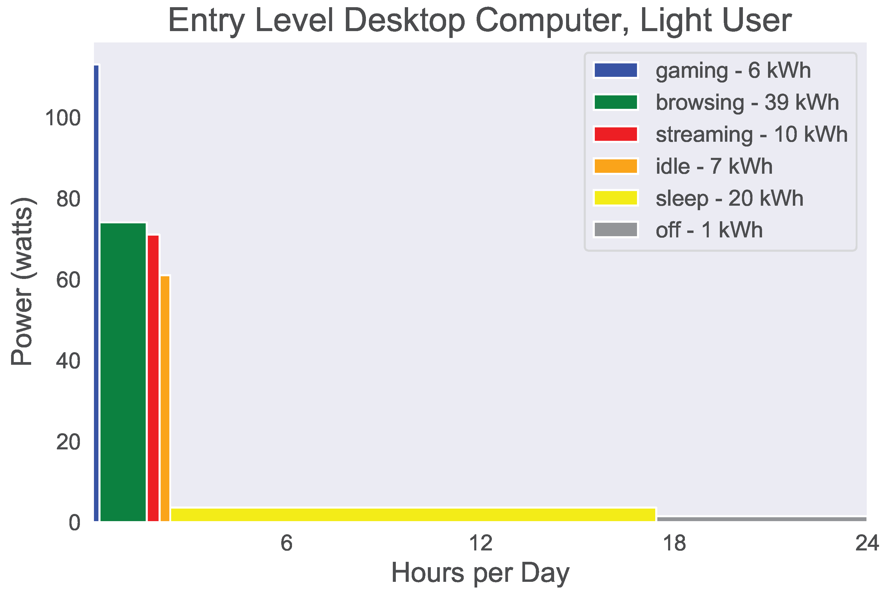
Figure 1. The distribution of a computer’s power modes with respect to time [12]. For an entry-level desktop with light use, standby modes account for 25% of the total energy consumption.
Electronics 08 00570 g001
Figure 2. A portfolio of standby reduction techniques and solutions. The solutions discussed in this paper are shown in the bright green boxes with bold font.
Electronics 08 00570 g002
Figure 3. Burst mode requires a supply capacitor and its necessary recharge logic. Converters without built-in burst mode can still be used in burst mode if they have an enable (EN In) pin.
Electronics 08 00570 g003
Figure 4. A simple design for the burst mode logic. The resistor divider scales the supply capacitor voltage, which is compared to high and low references. The reference voltages can be generated by nano-watt band gap references or low dropout regulator (LDOs). The comparators drive an SR latch, which determines if the converter is enabled.
Electronics 08 00570 g004
Figure 5. Oscilloscope waveforms with the supply capacitor voltage (yellow), low threshold comparator output (green), and high threshold comparator output (blue). These waveforms are from the PG02S2405A, loaded with a 4.7 kΩ resistor.
Electronics 08 00570 g005
Figure 6. A footer switch connects the device ground to the supply ground. A wake-up signal is required to drive the gate of the footer switch.
Electronics 08 00570 g006
Figure 7. A header switch topology. The wake-up signal activates an NMOS, which activates the PMOS header switch through a pull-up resistor.
Electronics 08 00570 g007
Figure 8. A cascoded header switch topology with example transistor values for a 48 V DC supply. The biasing network functions to bias the gate of M2 at 10 V. The pull-up network contains a Zener diode to protect the gate of the header switch M3. The latch is not shown.
Electronics 08 00570 g008
Figure 9. Proposed IR energy harvesting method for set-top boxes: (a) when the power button is pressed, a high power IR signal is transmitted to wake the device; and (b) once the device is awake, ordinary low power IR signals can be used for all other functions (e.g., changing the channel).
Electronics 08 00570 g009
Figure 10. The receiver for a zero standby supply with an IR-based wakeup signal. The photodiode harvests IR energy from the IR signal, which drives the gate of the footer switch.
Electronics 08 00570 g010
Figure 11. A prototype of the IR-based zero standby supply. The transmitter with four IR LEDs is shown on the left, the receiver with 12 dark photodiodes and the device (LCD screen) are shown on the right.
Electronics 08 00570 g011
Figure 12. Laser standby solution with a four-stage Dickson charge pump attached to an NMOS footer switch M1.
Electronics 08 00570 g012
Figure 13. The prototypes of the laser-based zero standby supply. (a) The charge pump prototype in a battery-powered lamp. The receiver is shown on the left, the laser on the right, and the low power IR remote on the top, which would contain the laser, in practice. (b) The cascoded header prototype in a 48 V power over ethernet PoE application.
Electronics 08 00570 g013
Figure 14. The microwatt wake-up radio can share an antenna with the high-power transceiver.
Electronics 08 00570 g014
Figure 15. Block diagram for how the WuR can be used to reduce standby power consumption in plug loads. The supply capacitor and burst mode logic provide a constant supply of microamp current to the wake-up radio. If the WuR needs to communicate with the main device, the circuit will require a header switch.
Electronics 08 00570 g015
Figure 16. Prototype of the WuR method for standby power reduction. Includes the transmitter (right), receiver (bottom left), and display load (top). All of the receiver board components can be integrated into the WuR except for the electrolytic supply capacitor.
Electronics 08 00570 g016
Table 1. PG02S2405A normal operation.
Load Resistance (Ω)Average Input Power (mW)Average Output Power (mW)Efficiency (%)
470153.552.134.0
470095.45.25.5
47,00090.70.520.6
Table 2. PG02S2405A burst mode.
Load Resistance (Ω)Average Input Power (mW)Average Output Power (mW)Efficiency (%)
47080.336.445.3
470014.93.926.0
47,0008.50.44.6
Table 3. OKX-T/5-D12N-C normal operation.
Load Resistance (Ω)Average Input Power (mW)Average Output Power (mW)Efficiency (%)
470528.052.710.0
4700476.15.31.1
47,000473.60.50.1
Table 4. OKX-T/5-D12N-C burst mode.
Load Resistance (Ω)Average Input Power (mW)Average Output Power (mW)Efficiency (%)
470177.536.820.7
470044.23.88.6
47,00029.50.41.3