Communication

A Design Methodology and Analysis for Transformer-Based Class-E Power Amplifier

1
School of Electrical and Electronic Engineering, Nanyang Technological University, Singapore 639798, Singapore
2
GLOBALFOUNDRIES, Singapore 738406, Singapore
3
School of Microelectronics, Tianjin University of China, Tianjin 300027, China
*
Authors to whom correspondence should be addressed.
Electronics 2019, 8(5), 494; https://doi.org/10.3390/electronics8050494
Submission received: 28 March 2019 / Revised: 25 April 2019 / Accepted: 26 April 2019 / Published: 2 May 2019
(This article belongs to the Section Microwave and Wireless Communications)

Abstract

:
This paper proposes a new technique and design methodology on a transformer-based Class-E complementary metal-oxide-semiconductor (CMOS) power amplifier (PA) with only one transformer and two capacitors in the load network. An analysis of this amplifier is presented together with an accurate and simple design procedure. The experimental results are in good agreement with the theoretical analysis. The following performance parameters are determined for optimum operation: The current and voltage waveform, the peak value of drain current and drain-to-source voltage, the output power, the efficiency and the component values of the load network are determined to be essential for optimum operation. The measured drain efficiency (DE) and power-added efficiency (PAE) is over 70% with 10-dBm output power at 2.4 GHz, using a 65 nm CMOS process technology.

1. Introduction

With the explosive growth of wireless and mobile communication systems adoption, the demand for compact, low-cost and low power portable transceiver has increased dramatically. One of the technical issues that is generally encountered for the portable transceivers is the limited lifetime of the battery. The power amplifier (PA) is typically the most power-hungry building block in the transceiver. Therefore, the design of a high-efficiency radio frequency (RF) PA is the most important solution to overcoming the battery lifetime limitation in portable communication systems. The class-E PA as depicted in Figure 1 has a maximum theoretical efficiency of 100%. It consists of a single output transistor that is driven as a switch and a passive load network. The passive load network is designed to minimize the drain voltage and current waveforms from overlapping [1], which causes output power loss. The major difference between class-E PA and others (e.g., Classes A, B, AB, C, D and F) is that it incorporates the parasitic drain-source capacitance [2] as part of the passive load network design, which is an advantage especially in CMOS design. In class-E PA, the circuit operation is determined by the transistor when it is on, and by the transient response of the load network when the transistor is off [2]. It greatly reduces the transistor power losses during the off-to-on transition of the device, resulting in high efficiency. To minimize these power losses, the following two conditions need to be met [1,2,3]:
V D S ( t = t 1 ) = 0
d V D S d t | t = t 1 = 0
In the conventional class-E PA, the RF-choke (RFC) is assumed to have a sufficiently high reactance and the output current through the load resistor R L is essentially a sinusoid at fundamental frequency. Under these conditions, the analytical design equations can be derived and are given by [4]:
R L = 0.5768 · V D D 2 R L
C 1 = 0.1836 · 1 ω R L
L x = 1.1525 · R L ω
where ω = 2 π f, and f= 2.4 GHz, V D D and Pout are the operating frequency, supply voltage and the desired output power, respectively. The combination of L 2 = 0.34 nH and C 2 = 12.88 pF forms a harmonic filter that is tuned to the operating frequency of the class-E PA. The major drawback of the class-E PA is the presence of high drain voltage when the switch is opened. This value is, in the ideal case, given by [5]
V D S , m a x = 2 π [ π 2 a r c t a n ( π 2 ) ] · V D D 3.562 · V D D
and the value of V D S , m a x threatens the transistor’s reliability, especially in CMOS technology, due to its low breakdown voltage. The maximum drain voltage can be alleviated by using a finite inductance instead of RF-choke, whereby the peak voltage can be reduced to 2.5 · V D D [6]. This paper presents an analysis and design methodology on transformer-based class-E PA involving the circuit equations, the relationships among the transistors switching “on-off” and the load quality factor (Q) at the resonant frequency ( f o ) of the load network, The basic performance and design parameters are discussed in this paper as well. Experimental results are demonstrated and they are in good agreement with the theories.

2. Methodology and Implementation on Transformer-Based Class-E PA

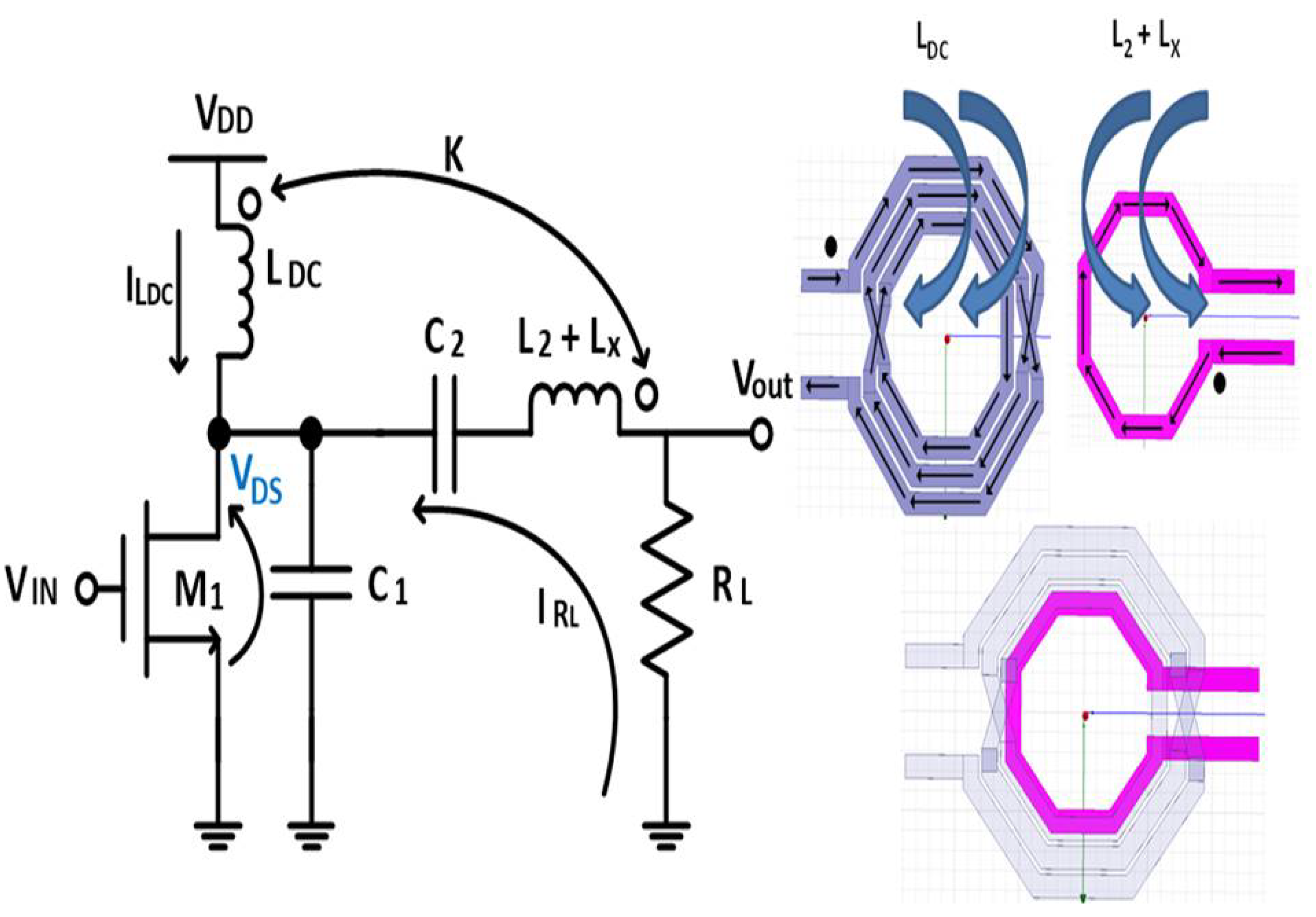
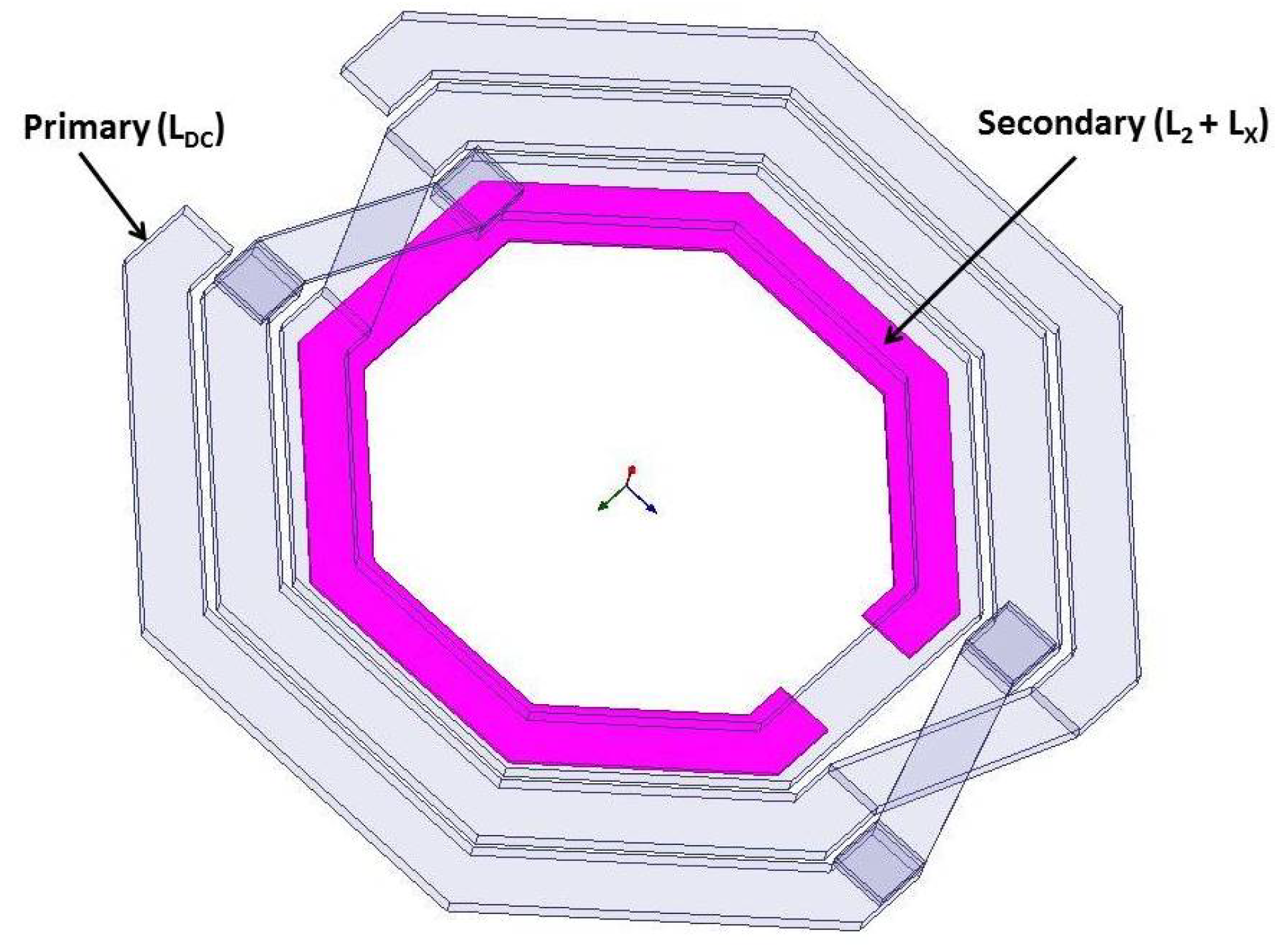
2.1. Design of the Inductors with Magnetic Coupling

The proposed transformer-based class-E PA with a finite DC-feed inductor is shown in Figure 2. The two coupled inductors (DC-feed and output series inductors) are inter-wound to form a transformer. The amount of coupling between the two inductors is quantified by defining a mutual magnetic coupling denoted as k, which can take on any value between one and zero. For the two coupled inductors ( L D C and L 2 + L X ), k and mutual inductance (M) are related by:
k = M L D C ( L 2 + L X )
A simplified transformer model is shown in Figure 3. This is modeled as two inductors, but with the addition of k between them and inter-winding capacitance C I W from input to output [7].
Note that the open-circle dots on inductors in Figure 2 are placed such that if current flows in the indicated direction, then there is a summation of magnetic fluxes [8]. Thus, the inductance reinforces itself and for a given inductance, the designs of both the L D C and L 2 + L X have shorter lengths (shortened approximately by 437 um) which implies lesser series resistance R S . This would allow a higher quality factor Q to manifest in the on-chip inductors, which translates to higher efficiency. In basic physics, the Q is defined as (8), where Z i n d is the impedance of the inductor.
Q = 2 π E n e r g y S t o r e d E n e r g y D i s s i p a t e d p e r C y c l e = | I m ( Z i n d ) | | R e ( Z i n d ) | = ω L R S
According to Faraday’s law of induction [9] states that the induced electro-motive-force ( ε ) through a coil is equal to the negative of the time rate of change of the magnetic flux ( ϕ B ):
ε = d ϕ B d t
The ϕ B through the coil is proportional to the magnetic field (B), which in turn is proportional to the current I in the coil.
ϕ B B ; B I ϕ B I
From Equations (9) and (10), we conclude that the induced ε is proportional to the negative of the time rate of change of the current.
ε d I d t ε = L d I d t
where L is the inductance of the coil. For a given rate of change of the current, the induced back emf increases with the inductance. Therefore, the inductance of a coil is a measure of its opposition to a change in current. Using Equation (11), we can express the inductance as:
L = ε d I / d t
Equating Equations (9) and (11)
ε = d ϕ B d t = L d I d t d ϕ B d t = d L I d t ϕ B = LI
Therefore, the inductance of a coil is also given by
L = ϕ B I

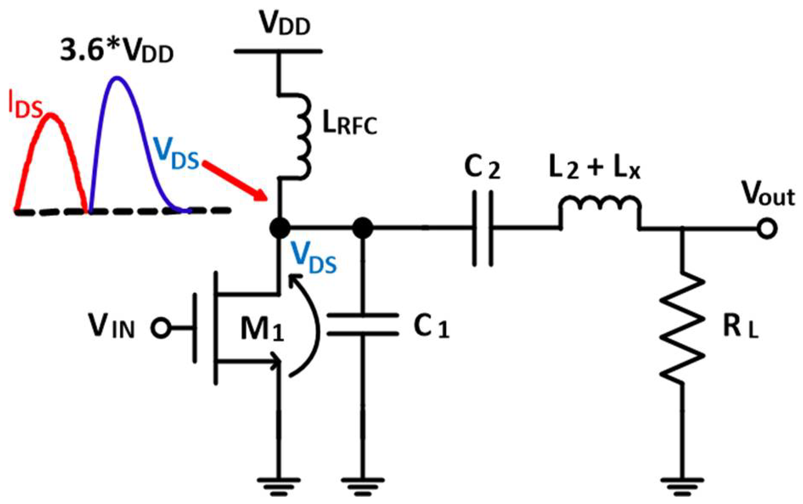
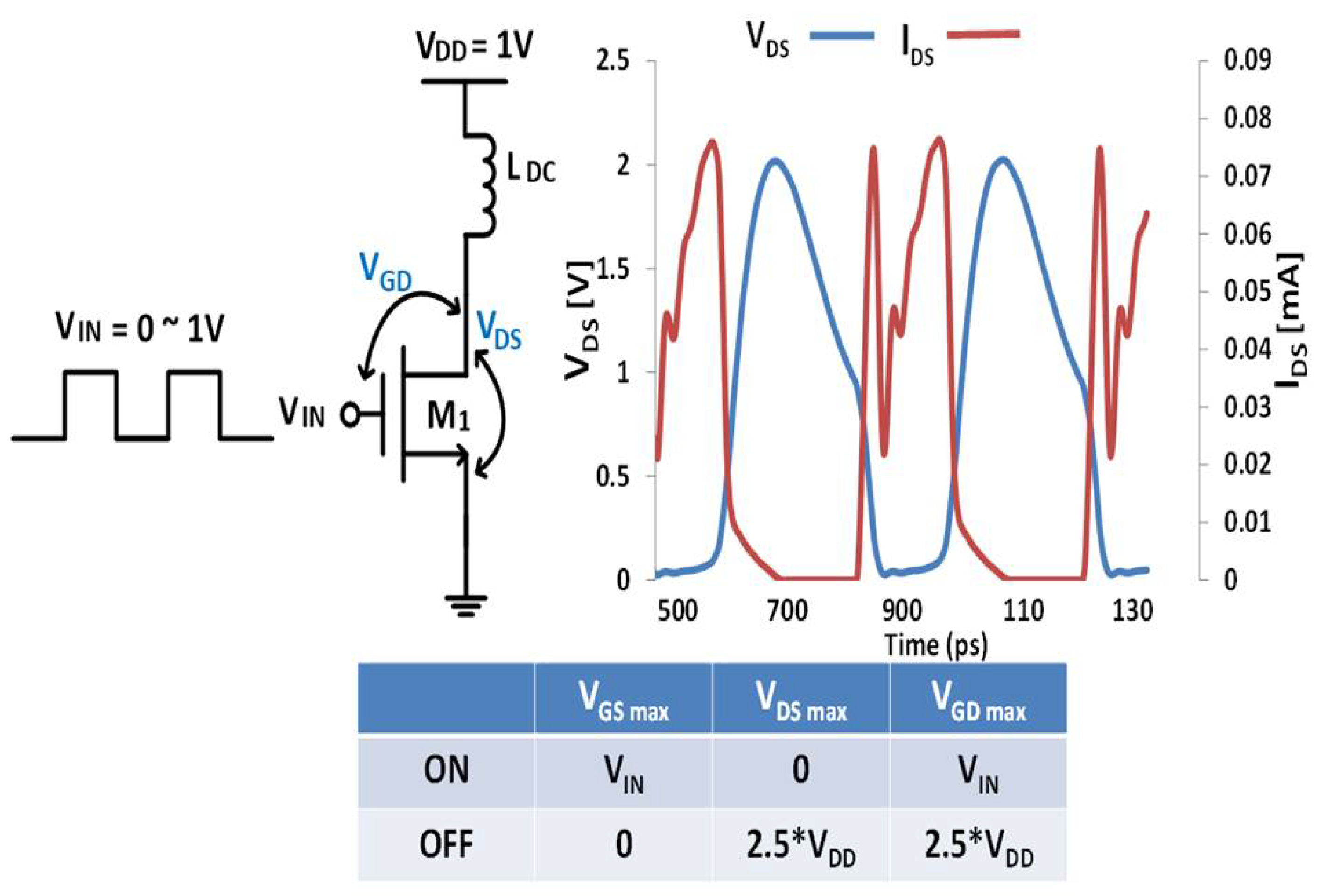
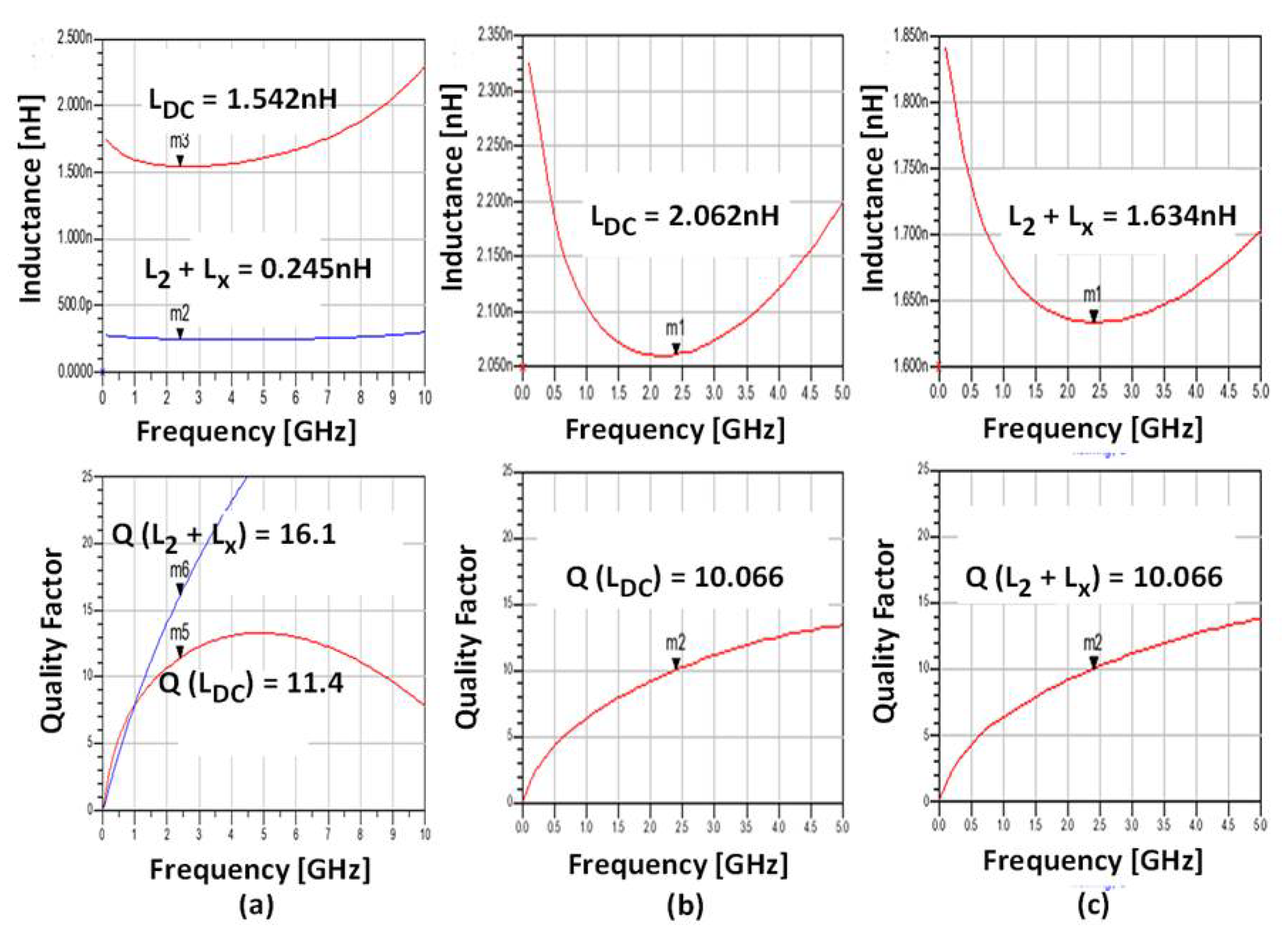
2.2. Design of the DC-Feed Inductance

There are two main reliability issues in the design of power amplifiers in submicron CMOS, namely oxide breakdown and the hot carrier effect. They increases the threshold voltage and, consequently degrades the devices’ performance. The key property of class-E PA is separation of drain voltage and drain current in the time domain. In this regard, high voltage and high current never coincide and when the transistor starts to conduct current, the drain voltage is close to zero due to the load network. As such, the class-E PA is limited by the oxide breakdown but not the hot carrier effect. This will set limits for the maximum drain voltage equal to the oxide breakdown voltage of the NMOS transistor. A major drawback is the maximum voltage stress on the transistor, V D S , m a x , which can be as high as 3.57 · V D D . Using a finite inductance instead of an RF-choke, the peak voltage can be reduced to 2.5 · V D D as shown in Figure 4 [6]. A common practice [10] is to keep the maximum voltage drop across the transistor below two times the nominal supply voltage ( V D D n o m = 1.2 V) to ensure reasonable device and circuit life-time.
The class-E PAs can be categorized into two types according to the inductor’s function: Class-E PA with RF-choke inductor or with DC-feed inductor. The proposed PA with a finite DC-feed inductor is shown in Figure 2. Using a finite DC-feed inductor instead of a large RF-choke in the class-E PA has several advantages [11] including:
  • Greatly reduce the loss due to a smaller electrical series resistance
  • A reduction in overall size and cost
  • Simplifying the design of the matching network

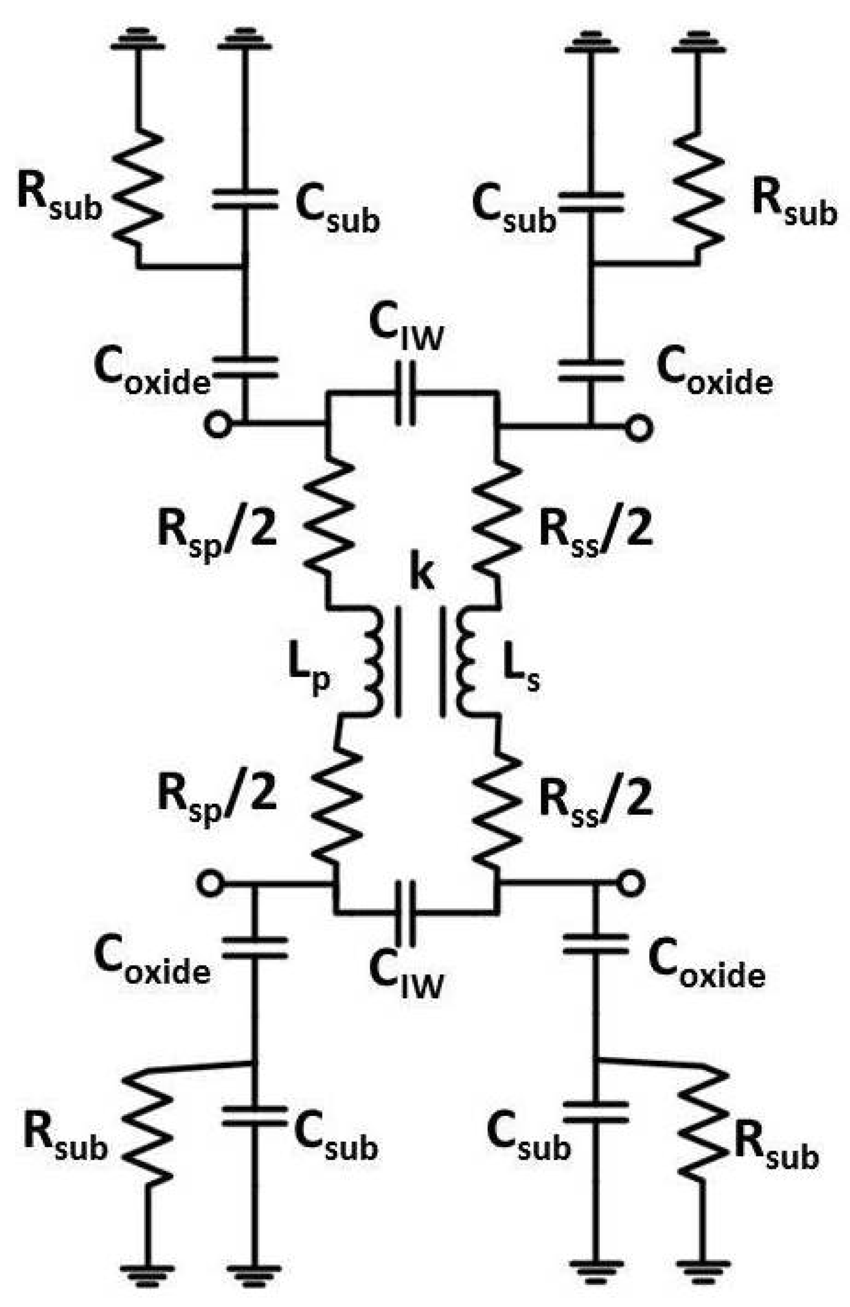
2.3. Design of Inductors and Transformers

Among all the passive structures used in RF circuits, high-quality inductors and transformers are the most difficult to realize monolithically. In silicon, they suffer from the presence of lossy substrate and high-resistivity metal. Therefore, well-designed inductors and transformers are very crucial and they must exhibit the following properties [12]:
  • Low series resistance in the primary and secondary windings
  • High magnetic coupling between the primary and the secondary coils
  • Low capacitive coupling between primary and the secondary coils
  • Low parasitic capacitances to the substrate
To obtain an optimum design of monolithic transformer on silicon we must follow closely the suggestions and guidelines provided as follows:
  • To minimize the series resistance and the parasitic capacitance, the spiral is implemented in the top metal layer (which is the thickest) [13]
  • It is desirable to minimize the outer dimensions of inductors, and this can be accomplished by decreasing W (line width) or incresing N (numbers of turns) [14]
  • A diameter of 5 to 6 times W should be chosen for the inner opening to ensure negligible coupling [15]
  • Differential geometry (driven by differential signals) also exhibits a higher Q [16], because each half experiences its own substrate loss and it will be reduced by a factor of two
  • Choose a line spacing S of approximately three times the minimum allowable value for the particular technology being used to fabricate the design
  • As a general rule of thumb, Din (inner dimension) lower than 50 μ m should be avoided unless it is mandatory to obtain very low inductance values (L < 0.5 nH) [17]
  • For multi-turn inductors, do not use very tight metal spacing (i.e., coil thickness/line spacing < 3) to limit the performance degradation as this will cause the proximity effects to become worse [18]
ANSYS High Frequency Structure Simulator (HFSS) was used to design and simulate the transformer structure and is shown in Figure 5. The primary inductor has an outer dimension of 187 μ m and a thickness of 3.3 μ m while the secondary inductor has an outer dimension of 122 μ m and a thickness of 0.9 μ m. Both of them have a line width of 12 μ m. This geometry has better symmetry compared with traditional inductors (its S parameters look the same from either side).

2.4. Transformer Layouts in Class-E PA

Another important aspect is to choose an appropriate transformer configuration to maximize the coupling between coils. Only two types provide acceptable performance; stacked [19] and interleaved [19,20] transformers. An interleaved transformer is built by two inductors fabricated using the same metal layer whose coils (i.e., metal layers) are laterally interleaved. The interleaved topology provides full symmetry but has poor magnetic coupling. A stacked transformer is made up of two identical inductors fabricated using different metal layers placed on top of each other. Stacked topology gives higher coupling factors, but the two inductors have different electrical parameters due to different metal layers.
The main advantages and drawbacks of these two configurations are presented in Table 1. The magnetic coupling between winding is measured by the magnetic coupling factor (k), which is typically around 0.7–0.9 for a monolithic transformer due to poor confinement of the magnetic flux.
The stacked transformer is adopted in this design to increase the quality factor Q, but at the expense of increased capacitance to the substrate and a resultant decrease in self-resonant frequency. This technique is of benefit for small inductors for which the substrate loss is not dominant and the design is at low enough frequency, safely away from the self-resonant frequency. Note that the magnetic fluxes through the two windings will renforce one another and the total inductance of the structure will be larger. As a result, the inductors will have a higher quality factor Q. The quality factor Q of the coupled inductors (Q of L D C = 11.4; Q of L 2 + L X = 16.1), uncoupeld Q of L D C and L 2 + L X are about 10 as shown in Figure 6.

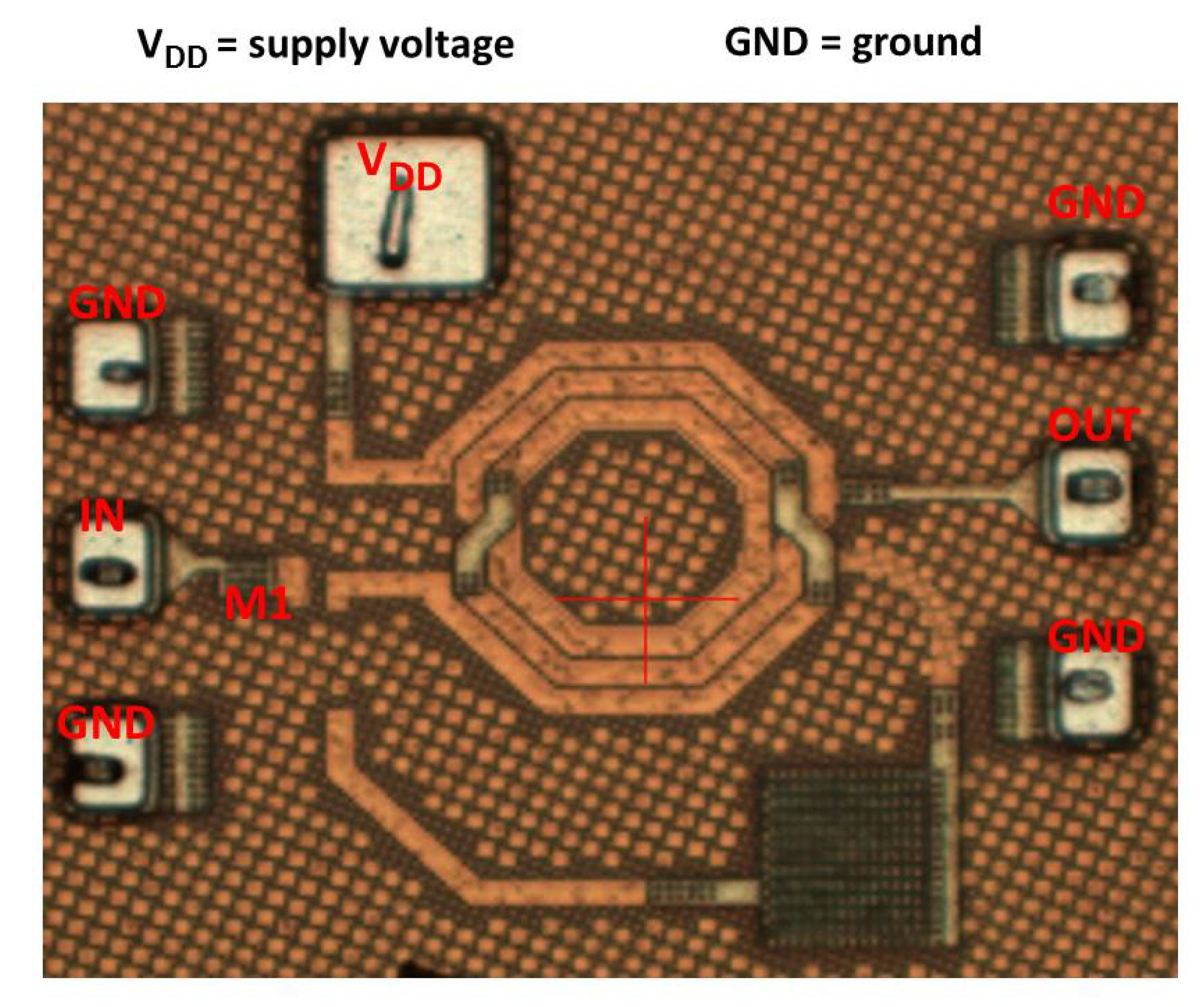
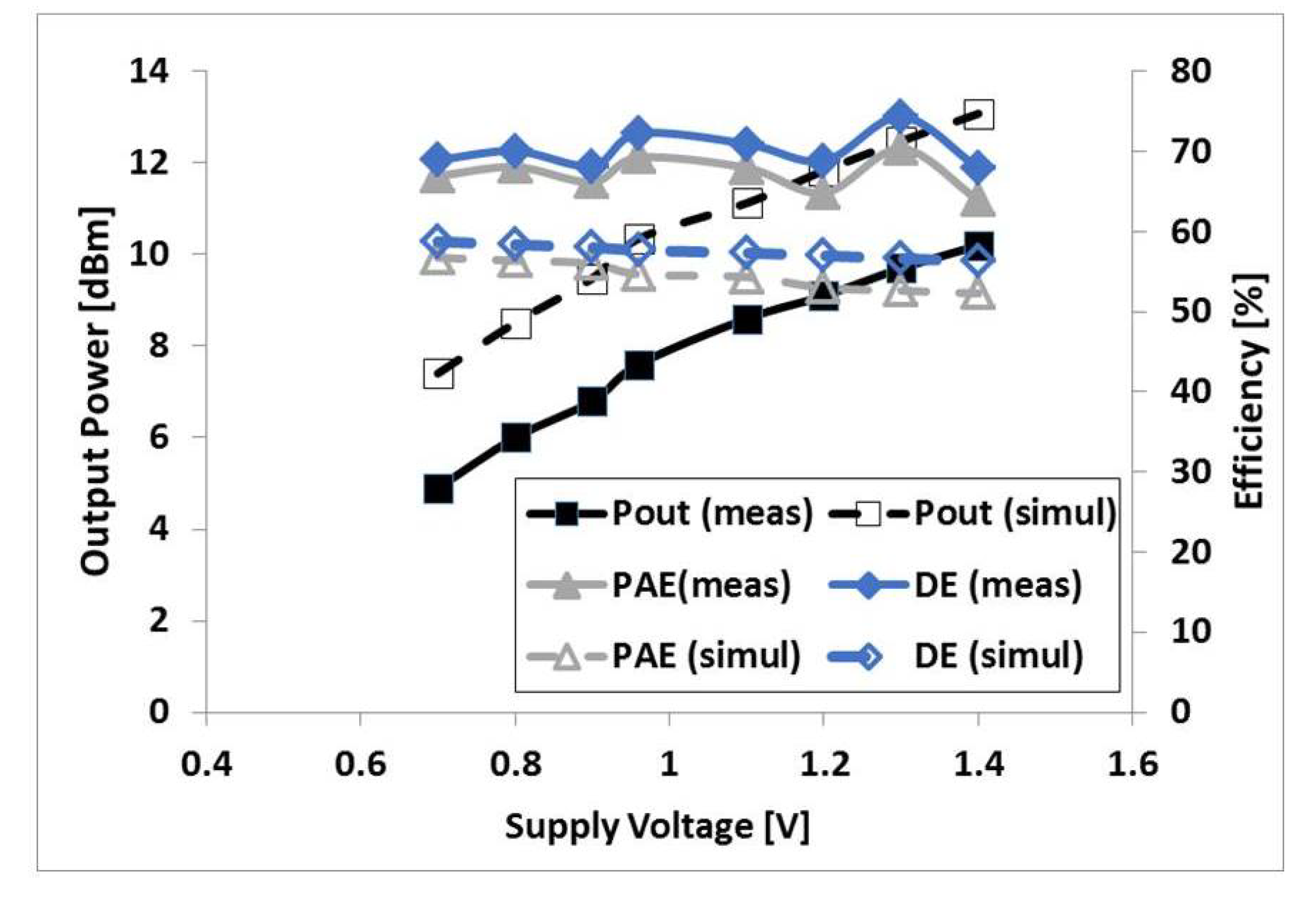
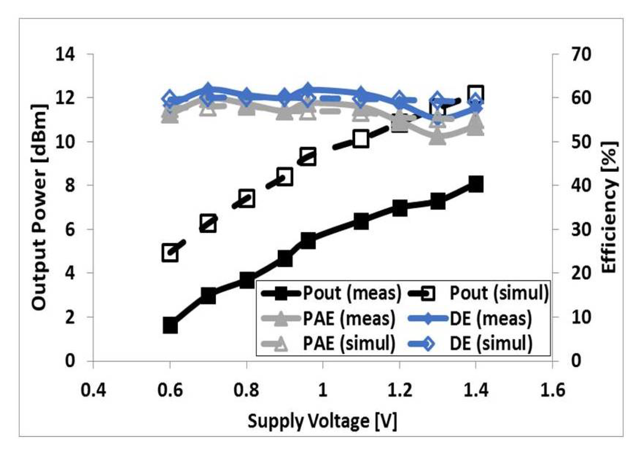
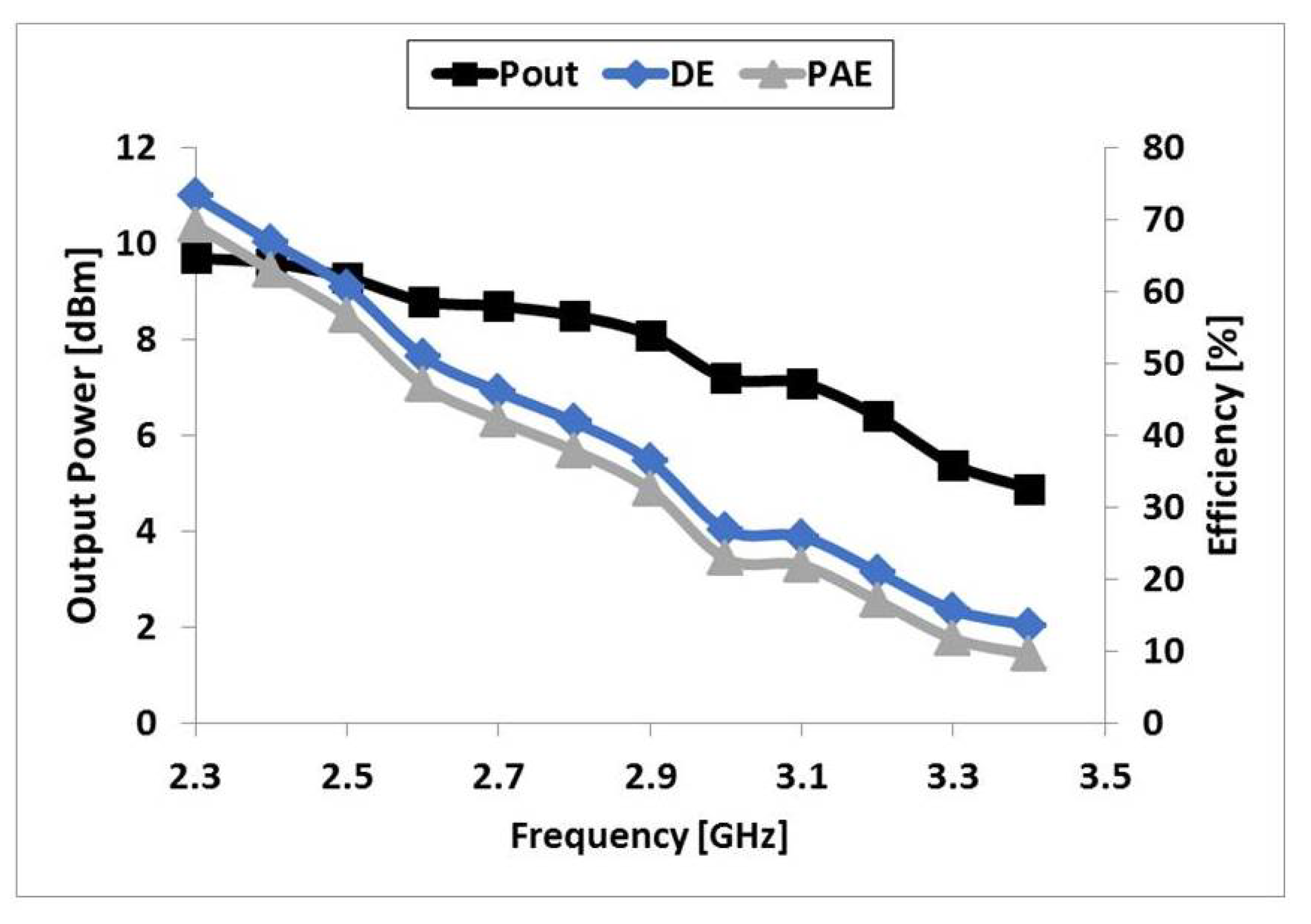
3. Measurement Results

The proposed methodology was implemented with a 2.4 GHz transformer-based class-E PA fabricated in GLOBALFOUNDRIES’ 65 nm CMOS process, and it occupies an area of 0.49 × 0.43 mm 2 including the I/O pads. The microphotograph of the fabricated PA is shown in Figure 7 and the measurement results of the design, i.e., transformer-based class-E PA based on differential inductors topology, and conventional uncoupled class-E PA are illustrated in Figure 8 and Figure 9 respectively. The simulation results are appended in the same figures as well.
The measurements are performed for the PA using on-wafer probing with E4407B network analyzer and Cascade Elite 300. The large-signal behavior of the PA is characterized from 1.2 to 3.4 GHz in steps of 0.1 GHz. All large-signal measurements are presented as the mean from 4 die samples with the inclusion of cable and probe loss of 1 dB.
In Figure 8 when V D D = 1.4 V, the PA deliver an output power of 10-dBm, and maximum DE and PAE were measured as 74% and 70% at a frequency of 2.4 GHz. Figure 10 shows the output power, DE and PAE over the range from 2.3 to 3.4 GHz. As can be seen in Figure 10, the output power is reduced by 4.8 dBm over the frequency range. The hypothesis of this decrease is that it could be due to the skin effect which results in a higher series resistance at higher frequencies as well as the parasitic drain capacitance but investigation are still ongoing. The following Figure-of-Merit (FoM) [21] is used to compare the performance of the designed chip with state-of-the-art CMOS switch-mode PAs (SMPAs) [21,22,23,24,25,26,27,28]:
FoM = PAE · freq [ Hz ] 0.25 chip size [ mm 2 ]
Due to its high efficiency (PAE = 70%) as shown in Figure 8 and compact size (die area = 0.21 mm 2 ) including the I/O pads, the proposed design methodology implemented on this work, has a FoM of 735, which is the highest among all designs in comparison as shown in Table 2.

4. Conclusions

In this paper, we presented a proposed methodology on the design of transformer-based class-E PA implemented in 65 nm CMOS technology. The class-E operating principles were reviewed and the design is based on transformer coupling effect to simultaneously reduce the chip area and improve the quality factor Q of the inductors. The methodology implemented allows the PA to deliver 10-dBm output power with 74% DE and 70% PAE at 2.4 GHz using the 65 nm CMOS process.

Author Contributions

A.L. conceptualized and designed the parameters; A.L. interpreted some results and wrote the paper; A.T. interpreted some of the results; Z.H.K. advised and proof-read the manuscript. K.M. provide simulation resources.

Funding

This research received no external funding.

Conflicts of Interest

The authors declare no conflict of interest.

References

  1. Sokal, N.O.; Sokal, A.D. Class E-A new class of high-efficiency tuned single-ended switching power amplifiers. IEEE J. Solid-State Circuits 1975, 10, 168–176. [Google Scholar] [CrossRef]
  2. Raab, F. Idealized operation of the class E tuned power amplifier. IEEE Trans. Circuits Syst. 1977, 24, 725–735. [Google Scholar] [CrossRef]
  3. Kazimierczuk, M. Exact analysis of class E tuned power amplifier with only one inductor and one capacitor in load network. IEEE J. Solid-State Circuits 1983, 18, 214–221. [Google Scholar] [CrossRef]
  4. Milosevic, D.; van der Tang, J.; van Roermund, A. Explicit design equations for class-E power amplifiers with small DC-feed inductance. In Proceedings of the 2005 European Conference on Circuit Theory and Design, Cork, Ireland, 2 September 2005; Volume 3, pp. 101–104. [Google Scholar] [CrossRef]
  5. Kazimierczuk, M. Collector amplitude modulation of the class E tuned power amplifier. IEEE Trans. Circuits Syst. 1984, 31, 543–549. [Google Scholar] [CrossRef]
  6. Johansson, T.; Fritzin, J. A Review of Watt-Level CMOS RF Power Amplifiers. IEEE Trans. Microw. Theory Tech. 2014, 62, 111–124. [Google Scholar] [CrossRef] [Green Version]
  7. Long, J.R.; Copeland, M.A. The modeling, characterization, and design of monolithic inductors for silicon RF IC’s. IEEE J. Solid-State Circuits 1997, 32, 357–369. [Google Scholar] [CrossRef]
  8. Sadiku, M.N. Elements of Electromagnetics; Oxford University Press: Oxford, UK, 2014. [Google Scholar]
  9. Gamo, H. A general formulation of Faraday’s law of induction. Proc. IEEE 1979, 67, 676–677. [Google Scholar] [CrossRef]
  10. Mazzanti, A.; Larcher, L.; Brama, R.; Svelto, F. Analysis of reliability and power efficiency in cascode class-E PAs. IEEE J. Solid-State Circuits 2006, 41, 1222–1229. [Google Scholar] [CrossRef]
  11. Acar, M.; Annema, A.J.; Nauta, B. Analytical Design Equations for Class-E Power Amplifiers with Finite DC-Feed Inductance and Switch On-Resistance. In Proceedings of the 2007 IEEE International Symposium on Circuits and Systems, New Orleans, LA, USA, 27–30 May 2007; pp. 2818–2821. [Google Scholar] [CrossRef]
  12. Lopez-Villegas, J.M.; Sieiro, J. Modeling of integrated inductors and transformers for RF applications. In Proceedings of the 6th International Conference on Thermal, Mechanial and Multi-Physics Simulation and Experiments in Micro-Electronics and Micro-Systems (EuroSimE 2005), Berlin, Germany, 18–20 April 2005; pp. 19–23. [Google Scholar] [CrossRef]
  13. Razavi, B.; Behzad, R. RF Microelectronics; Prentice Hall: Upper Saddle River, NJ, USA, 1998; Volume 1. [Google Scholar]
  14. Jenei, S.; Nauwelaers, B.K.J.C.; Decoutere, S. Physics-based closed-form inductance expression for compact modeling of integrated spiral inductors. IEEE J. Solid-State Circuits 2002, 37, 77–80. [Google Scholar] [CrossRef]
  15. Mohan, S.S.; del Mar Hershenson, M.; Boyd, S.P.; Lee, T.H. Simple accurate expressions for planar spiral inductances. IEEE J. Solid-State Circuits 1999, 34, 1419–1424. [Google Scholar] [CrossRef]
  16. Danesh, M.; Long, J.R.; Hadaway, R.A.; Harame, D.L. A Q-factor enhancement technique for MMIC inductors. In Proceedings of the 1998 IEEE MTT-S International Microwave Symposium Digest, Baltimore, MD, USA, 7–12 June 1998; Volume 1, pp. 183–186. [Google Scholar] [CrossRef]
  17. Sia, C.; Ong, B.; Chan, K.; Yeo, K.; Ma, J.; Do, M.A. Physical layout design optimization of integrated spiral inductors for silicon-based RFIC applications. IEEE Trans. Electron Devices 2005, 52, 2559–2567. [Google Scholar] [CrossRef]
  18. Scuderi, A.; Biondi, T.; Ragonese, E.; Palmisano, G. Analysis and modeling of thick-metal spiral inductors on silicon. In Proceedings of the 2005 European Microwave Conference, Paris, France, 4–6 October 2005; Volume 1. [Google Scholar] [CrossRef]
  19. Zolfaghari, A.; Chan, A.; Razavi, B. Stacked inductors and transformers in CMOS technology. IEEE J. Solid-State Circuits 2001, 36, 620–628. [Google Scholar] [CrossRef]
  20. Long, J.R. Monolithic transformers for silicon RF IC design. IEEE J. Solid-State Circuits 2000, 35, 1368–1382. [Google Scholar] [CrossRef]
  21. Wei, M.; Kalim, D.; Erguvan, D.; Chang, S.; Negra, R. Investigation of Wideband Load Transformation Networks for Class-E Switching-Mode Power Amplifiers. IEEE Trans. Microw. Theory Tech. 2012, 60, 1916–1927. [Google Scholar] [CrossRef]
  22. Tan, J.; Heng, C.; Lian, Y. Design of Efficient Class-E Power Amplifiers for Short-Distance Communications. IEEE Trans. Circuits Syst. I Regul. Pap. 2012, 59, 2210–2220. [Google Scholar] [CrossRef]
  23. Apostolidou, M.; van der Heijden, M.P.; Leenaerts, D.M.W.; Sonsky, J.; Heringa, A.; Volokhine, I. A 65 nm CMOS 30 dBm Class-E RF Power Amplifier With 60PAE at 16 dB Back-Off. IEEE J. Solid-State Circuits 2009, 44, 1372–1379. [Google Scholar] [CrossRef]
  24. Song, Y.; Lee, S.; Cho, E.; Lee, J.; Nam, S. A CMOS Class-E Power Amplifier With Voltage Stress Relief and Enhanced Efficiency. IEEE Trans. Microw. Theory Tech. 2010, 58, 310–317. [Google Scholar] [CrossRef]
  25. Ren, J.; Dai, R.; He, J.; Xiao, J.; Kong, W.; Zou, S. A novel stacked class-E-like power amplifier with dual drain output power technique in 0.18 μm RFSOI CMOS technology. In Proceedings of the 2018 IEEE MTT-S International Wireless Symposium (IWS), Chengdu, China, 6–10 May 2018; pp. 1–4. [Google Scholar] [CrossRef]
  26. Kreißig, M.; Kostack, R.; Pliva, J.; Paulo, R.; Ellinger, F. A fully integrated 2.6 GHz cascode class-E PA in 0.25 μm CMOS employing new bias network for stacked transistors. In Proceedings of the 2016 IEEE MTT-S Latin America Microwave Conference (LAMC), Puerto Vallarta, Mexico, 12–14 December 2016; pp. 1–3. [Google Scholar] [CrossRef]
  27. Li, P.; Xia, Q.; Chen, Z.; Geng, L. High efficiency triple-stacked class-E power amplifier with novel dynamic biasing network. In Proceedings of the 2018 IEEE MTT-S International Wireless Symposium (IWS), Chengdu, China, 6–10 May 2018; pp. 1–4. [Google Scholar] [CrossRef]
  28. Zhai, C.; Cheng, K.M. Fully-integrated CMOS differential class-E Power Amplifier with combined waveform-shaping network and transformer-based balun. In Proceedings of the 2014 Asia-Pacific Microwave Conference, Sendai, Japan, 4–7 November 2014; pp. 738–740. [Google Scholar]
Figure 1. ConventionalClass-E power amplifier (PA) using NMOS transistor with radio frequency RF-choke and series LC network.
Electronics 08 00494 g001
Figure 2. Transformer-Based Class-E PA: magnetic coupling and determining correct dot placement.
Electronics 08 00494 g002
Figure 3. Basic model of transformer.
Electronics 08 00494 g003
Figure 4. Maximum voltage stresses on transistor M1 in both on and off states.
Electronics 08 00494 g004
Figure 5. Schematic of on-chip transformer 3-D view
Electronics 08 00494 g005
Figure 6. The quality factor plotted versus frequency for the inductors: (a) Coupling-inductors; (b) DC-feed inductor; (c) Output series inductor.
Electronics 08 00494 g006
Figure 7. Microphotograph of the implemented power amplifier
Electronics 08 00494 g007
Figure 8. Transformer-based class-E PA: Output power, drain efficiency and power-added efficiency versus the DC supply voltage (measurement: solid black, blue and grey; simulation: dashed white, blue and grey).
Electronics 08 00494 g008
Figure 9. Uncoupled class-E PA: Output power, drain efficiency and power-added efficiency versus the dc supply voltage (measurement: solid black, blue and grey; simulation: dashed white, blue and grey). Drain efficiency (DE) and power-added efficiency (PAE)
Electronics 08 00494 g009
Figure 10. Transformer-based class-E PA: Measured output power, drain efficiency and power-added efficiency versus operating frequency.
Electronics 08 00494 g010
Table 1. Advantages and drawbacks of interleaved and stacked configurations.
ConfigurationsAreak f SR CapacitanceElectrical Symmetry
InterleavedMediumMediumExcellentExcellentExcellent
StackedExcellentExcellentMediumPoorMedium
Table 2. Comparison of state-of-the-art class-E PA designs. Figure-of-Merit (FoM).
Reference P out [dBm]PAE [%]f [GHz]Die Area [mm 2 ]Process [nm]FoM
[21]28.7482.31.290121.74
[22]5.7552.41130100.37
[23]306020.365423
[24]31.5511.81130111.23
[25]29.6511.81.518070
[26]21.737.92.61.2125070.7
[27]22.349.550.235250560
[28]2938.71.81.5335052
This Work10.7702.40.2165735

