1. Introduction
Since recently, natural disasters such as tsunamis, earthquakes, heavy rains, and strong winds caused by climate change, and the collapse of buildings and massive power outages can be accurately predicted and situations can be minimized by promptly communicating them to the public, and many countries have a variety of disaster networks.
For example, the United States created the Emergency Alert System (EAS) in 1994 to inform the public of the dangers of natural disasters such as typhoons, hurricanes, floods, tsunamis, earthquakes, and heavy snow, as well as emergencies such as fire, poisonous gas, power outages, and industrial accidents. In addition, the United States has a Federal Emergency Management Agency (FEMA) [
1] as an integrated alarm system, and has established an Integrated Public Alert and Warning System (IPAWS) to provide integrated communication to protect lives and properties. In Europe, the integrated communications for enhanced environmental risk management and citizens safety (CHORIST) project [
2] is ongoing. This improves the speed and effectiveness of coping with natural and industrial disasters, thereby optimizing citizen safety and communication among rescuers. Asian countries such as Korea, Japan, and China operate disaster broadcasting according to the communication standards of each country [
3,
4,
5].
For such a system, the existing disaster-broadcasting network uses analog signals such as FM and, with the development of digital broadcasting (e.g., Digital Multimedia Broadcasting (DMB)), and the introduction of personal mobile-reception devices, FM and DMB broadcasting networks have emerged as effective means for rapidly spreading information on disaster situations.
Terrestrial DMB can use video-/audio-/data-broadcasting services anytime and anywhere, and it can receive convenient information services such as news, weather, stock, navigation services, and mobile communication. In addition, because it can always be received by using a portable terminal, it has an optimal condition to use as disaster broadcasting. However, in a system for providing such services using wireless, a radio-shaded area occurs due to special topography and property between base stations constituting a wireless-communication service network. These spaces are very wide-ranging, from shopping malls, airports, and parking lots, which are fully open spaces, to fully enclosed mines, trains, or automobile tunnels. It is impossible to install base stations in all of these places due to cost and space issues.
In wireless communication, a repeater device capable of improving signal quality in such a radio-shaded area at low cost was researched and developed. Typically, the repeater was designed to amplify only the intensity of the signal by using an analog method; thus, reliability of communication quality is low. In this paper, however, we designed and implemented a repeater system with digital-signal-processing (DSP) algorithms using FPGA, which can reduce the radio-shaded area and increase reliability of the signal.
Traditionally, multiple standard integrated circuits are wired together to construct radios, Transport Network Controls (TNCs), and other systems. However, modern devices manufactured in high volume integrate numerous functionalities on a single chip that is customized for this specific purpose. Feature sizes in integrated circuits have now become so small that FPGA can be used to achieve what once required a custom chip. Since the logic in FPGA can be used in parallel rather than sequentially, it is a good solution to implement DSP algorithms for the repeater. Recently, FPGAs have also contained larger amounts of dedicated memory, making it possible to couple microprocessors (e.g., ARM-based) to design complicated systems [
6,
7].
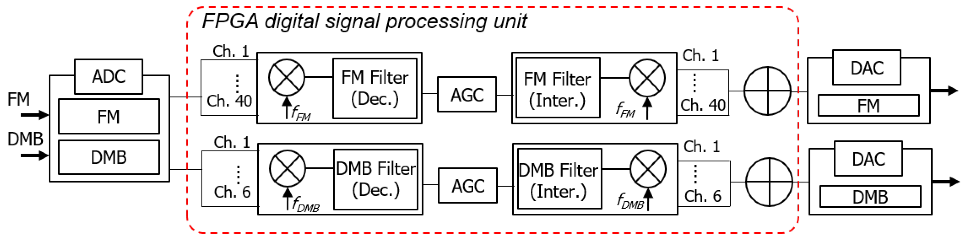
In this study, we designed digital circuits for a multichannel repeater for both FM and DMB signals by employing DSP algorithms and implementing them in FPGA. The proposed repeater can handle up to 40 FM and 6 DMB signals in parallel simultaneously with an automatic gain controller (AGC), which can maintain the output power level to a constant level. DSP algorithms include frequency-modulation and -demodulation schemes. In addition, three types of filters, the Cascaded Integrator Comb (CIC) filter, Finite Impulse Response (FIR) filter, and Interpolated Second Order Polynomial (ISOP) Filter are included in the system. The repeater system is implemented in Verilog HDL and tested on Xilinx Kintex 7 xc7k325tffg676- 1 as a target device.
The rest of the paper is organized as follows. In
Section 2, several related works are revisited. In
Section 3, the DSP algorithms used in the proposed repeater and design methodology are studied. Testing results are presented and analyzed in
Section 4. Finally,
Section 5 concludes the paper.
2. Related Work
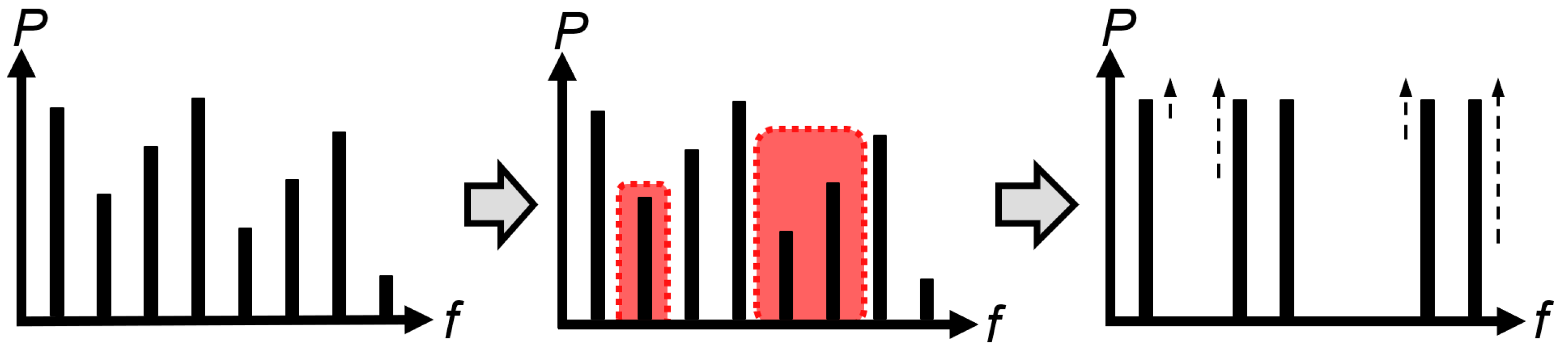
The basic operation of the digital repeater consists of receiving analog radio-frequency (RF) signals, eliminating unnecessary adjacent channels through filters, and amplifying the selected signals, as shown in
Figure 1. Since the digital repeater operates in an Intermediate Filtering (IF) band, the signal passes through a Digital Down Converter (DDC) and Digital Up Converter (DUC) [
8], then passes through a filter section and AGC. Digital repeaters are used in various band ranges and frequencies. Thus, in this Section, we discuss various RF repeater products that are used in the industry and the AGC that has been studied so far.
2.1. Industry Digital Repeaters
Many repeater companies manufacture digital repeaters that can be used in various radio-shaded areas such as tunnels and underground parking lots [
9], and they are used for different band ranges and frequencies.
In this Section, we introduce a repeater that complies with the Terrestrial Trunked Radio (TETRA) standard developed for public-safety communications in Europe among RF communication repeaters. Though the TETRA repeater is different than the repeater we propose in this paper in frequency bands, they are same in basic structure and format.
The first product is Cohbam Wireless’ BSR438 [
10]. This repeater was designed to amplify signals in a tunnel. Since the company did not disclose how the digital circuit is implemented internally, we inferred how it was designed from the provided specifications. The maximum bandwidth of the BSR438 is 5 MHz, and the minimum bandwidth is not revealed. The gain of this repeater is between 55 and 85 dBm, and the maximum group delay is 2 μs. The frequency band of the BSR438 is 380∼470 MHz, and it can operate up to four channels. The second is the same company’s product, the CSR238 FPGA-based repeater. The bandwidth of this repeater is 1∼5 MHz, and AGC is included to provide a maximum gain of up to 95 dBm. The frequency band is 148∼174 MHz and it can operate up to eight channels. The CSG9380 from CSG [
11] is a repeater with a 20∼90 kHz filter bandwidth, widely used for low-latency applications. The frequency band is 385∼400 MHz, and it can operate up to eight channels. The fourth is Selecom’s RF/RF TETRA/TETRAPOL [
12]. As the name suggests, this repeater is a dedicated RF and TETRA repeater. This repeater uses the frequency band of 380∼470 MHz, and supports a maximum gain of up to 90 dBm. The filter bandwidth is 300∼5000 kHz, and it supports up to eight channels. The fifth is the GC5018 [
13] repeater, which is by Texas Instruments. This repeater can support up to 115 dBm of maximum gain through additional AGC, and can process up to 16 channels at the same time. The main advantage of this repeater is that it provides various filter bandwidths and can be used at various frequencies. There are also TUCSYS products made by SEE Telecom [
9].
Table 1 summarized the properties of these industrial products.
2.2. Digital Repeaters Using FPGA
In recent years, FPGA-based repeaters have become more useful than ASIC-based repeaters because FPGAs are better in terms of reconfigurability and development time. Lattice, a manufacturer of FPGAs, shows the practical examples of how to implement a digital wireless-communication filter [
14,
15]. The structure of the repeater includes a digital mixer with Numerical Controlled Oscillators (NCO) implemented by a Direct Digital Synthesizer (DDS) Compiler [
16] and a plurality of filters.
Typical FPGA-based repeaters utilizing this method are presented in References [
17,
18]. These repeaters include DUC and DDC, and do not disclose internal modules and configurations in detail. The repeater in Reference [
17] is implemented using 16 DSP slices and only handles two channels. The output sample rate is 3.78 Megasamples Per Second (MSPS) with a decimation ratio of 1 and a latency of 265 ns. The filter was designed using FIR filter and NCO. Another manufacturer of a repeater [
18] did not disclose much information, but it uses seven DSP slices and NCO, and only operates for one channel without utilizing FIR filters. It uses a decimation ratio of 2 to process the signal. Although the GC5018 [
13] repeater is implemented and manufactured in application of a specific integrated circuit (ASIC), the performance of the repeater is similar to that of the repeater implemented in this paper. The GC5018 repeater has a latency of 151 ns and a sample rate of 7.68 MSPS. It operates 16 channels in parallel and has a decimation ratio of 6. Recently, a repeater that has a filter bandwidth of 5∼5000 kHz and maximum gain of 135 dBm, and can operate 8 channels in parallel was also proposed [
19].
Table 2 summarizes these repeaters.
Conventional FPGA-based repeaters cannot handle enough channels at the same time, and require a very high computation amount due to an extremely low decimation ratio. In this study, we implemented a FPGA-based repeater, which uses the DUC, DDC, various filters, NCO, and IPs described in the following section. With such a more sophisticated filtering operation, we were able to accurately remove adjacent channels and design a repeater that exhibits higher parallelism. In addition, through design optimization, we could implement a repeater that can simultaneously operate up to a total of 46 channels with a smaller amount of computation than conventional designs.
2.3. Digital Automatic Gain Controller (AGC)
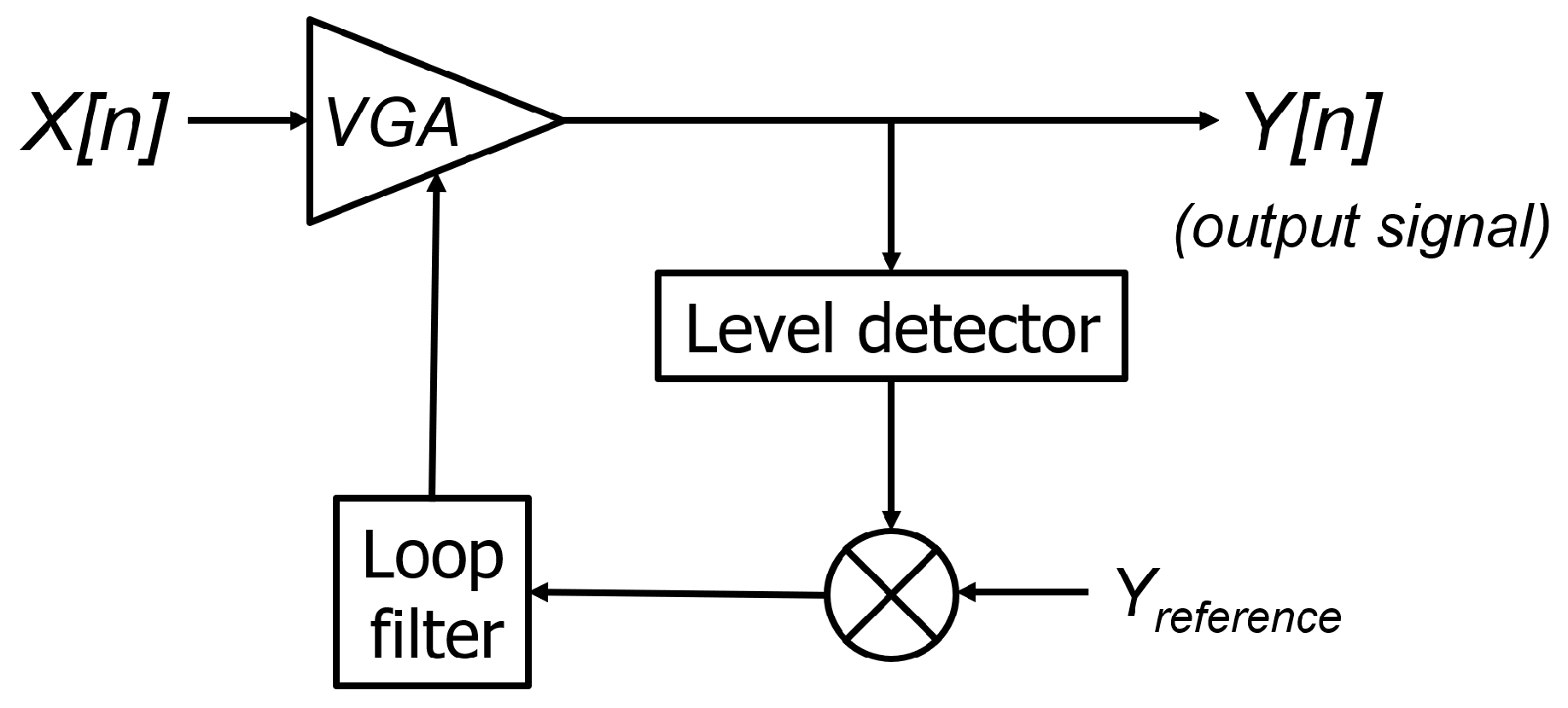
AGC is widely used in fields where the power of the input signal uses various dynamic range signals (sound, image processing, wireless communication, digital audio, radar, etc.). The goal of the AGC is to automatically keep the output power level constant. Many AGCs have been proposed and provided for each application using a loop-transfer function or a variable gain amplifier (VGA) structure, as shown in
Figure 2 [
20]. Research on digital AGCs has been progressing for decades. References [
21,
22] are examples of digital AGCs using conventional methods. Reference [
23] proposed a fast and robust scheme using an upcounter and an attenuator. A two-stage AGC algorithm for accurate gain adjustment was proposed in Reference [
24], and Reference [
25] proposed a new AGC method in which a simple digital algorithm-based implementation was successfully demonstrated without performance loss. More recently, Reference [
26] proposed an all-digital AGC architecture without filter and divider.
A conventional AGC is designed using an accurate level-detect and loop-transfer function, but it has the disadvantage of large computational complexity. Reference [
23] proposed a new method of level detection that detects the power of the AGC output and feeds it back to the AGC instead of detecting power inside AGC. However, the computational complexity and delay of the method are not significantly improved from a conventional AGC.
In this paper, we present an AGC with reduced computation needs and faster operation by simplifying the power-level detection scheme. The designed AGC can process multiple FM and DMB signals at the same time to increase versatility and allow users to select the gain level for user friendliness.
3. Digital-Signal-Processing Algorithm
In this section, we explain how to handle FM and DMB signals in digital format. Both FM and DMB are good means for disaster networks, as explained in the introduction. However, the properties of both signals are different. To design filters, we need to understand the basic characteristics of the FM and DMB signals. FM signals use a frequency band from 88 to 108 MHz, with a bandwidth of 0.15 MHz. The FM signal have a center-frequency signal without a subchannel. On the other hand, DMB signals utilize the frequency band from 174 to 216 MHz, and the bandwidth is 1.536 MHz. DMB signals use the method of orthogonal frequency-division multiplexing (OFDM) including many subchannels (or carriers) around one center frequency.
Table 3 summarizes the characteristics of FM and DMB signals.
3.1. FM Digital-Signal-Processing Algorithm
In this paper, we present a digital circuit that can handle 40 channels of FM signals in parallel. DSP algorithms are implemented to select the 40 strongest channels except the signals with low power among all received FM signals and adjust them to maintain the same output power level with AGC. As shown in
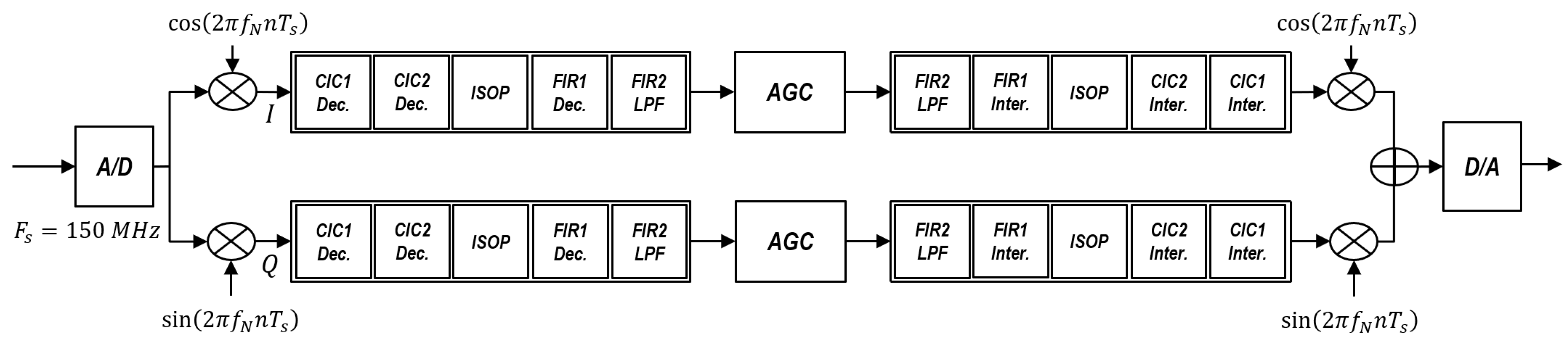
Figure 3, the proposed digital-processing circuit for FM signals consists of four digital mixers, four CIC filters, four ISOP filters, and two AGCs for the in-phase (I) and the quadrature (Q) components. The received FM analog signal is converted to a digital signal through an analog to a digital converter (ADC) (e.g., a 14-bit and 150 MHz sampling rate ADC is used in this study). The converted digital signal is downconverted to a baseband through a digital mixer. After passing through the digital mixer, the signal is split into the I and Q components, which pass through a filter section (i.e., the CIC decimator and ISOP) that effectively removes adjacent frequencies. The filtered signals then pass through the AGC, which compensates their power level. After that, the I and the Q components are recovered into the original frequency and combined. The signal is converted into an analog signal through a digital-to-analog converter (DAC) and then transmitted by the radio-frequency (RF) block.
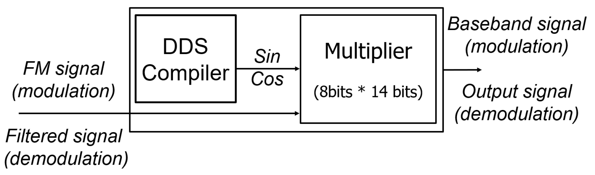
To efficiently process the input signals of various frequency ranges, the 14-bit digital signal must be transferred to the baseband (i.e., the same frequency for all channels). To move the input signals to a baseband, a digital mixer, which is widely used in wireless communication, is used, as shown in
Figure 4. A DDS compiler and a multiplier are used to design a digital mixer in FPGA. In general, a Finite Impulse Response (FIR) filter or an Infinite Impulse Response (IIR) filter can be used to filter the adjacent frequency of a signal that has passed through the digital mixer. These filters are simple to implement, but they require heavy multiplication operations in nature. In FPGA, multiplication increases the utilization of the DSP slice, which results in an increase in total power. Therefore, we instead exploit the Cascaded Integrator Comb (CIC) filter in the proposed circuit. This is because there is no multiplication operation in the CIC filter. The CIC filter is operated as a low-pass filter (LPF) that can filter the adjacent frequency of the downconverted signal to the baseband.
The transfer function of the digital CIC filter at sampling frequency
can be expressed as follows:
The optimal decimation ratio (
R), number of stages (
N), and number of samples per stage (
M) are calculated using MATLAB simulations [
27]. The numbers obtained from the simulation are
= 693,
= 6, and
= 1. The interpolation ratio is the same as the decimation.
For CIC filter implementation, Xilinx Vivado v17.4 provides CIC Compiler as an IP core [
28,
29]. If a CIC filter is designed using the provided IP core, low-power implementation is impossible because the CIC by the IP core utilizes DSP slices that consume a significant amount of power. Instead, CIC filters are designed directly by using a look-up table (LUT) method because it is impossible to implement the entire system (i.e., for multichannel FM and DMB) in limited resources (e.g., limited DSP slices) by the IP core compiler, and low-power design is possible if the CIC filter is designed using the LUT rather than the DSP slice. As a result, we can realize the CIC filter without DSP slices that occupy a large area and consume power. The comparison between the designed CIC filter and the automatically compiled CIC filter in resource utilization and power consumption are shown in
Table 4 and
Table 5, respectively. As shown, the designed CIC filter requires less utilization in LUTRAM, FF, and DSP except LUT, and power consumption is approximately 2.23 times less than the CIC filter generated by the Xilinx compiler.
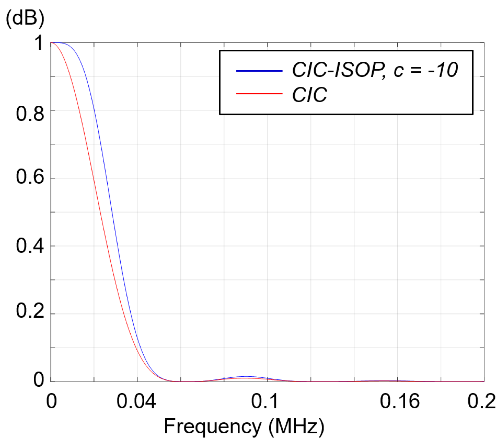
We used a CIC filter for FM signal processing. However, as shown in
Figure 5, the larger the decimation ratio of the CIC decimator filter, the worse the pass-band droop phenomenon and the lower the performance of the entire filter. When decimation ratio
is 40, as shown in
Figure 5a, it can be seen that the band-pass droop phenomenon occurs. On the other hand, when using decimation ratio
of 25, as shown in
Figure 5b, the band-pass droop phenomenon is reduced significantly. Thus, we added an ISOP filter, as shown in
Figure 3, to compensate the pass-band droop phenomenon of the CIC filter because we needed a large decimation ratio (e.g.,
= 693).
The transfer function of the digital ISOP filter of output
is defined as follows:
We used a coefficient
c of −10 in the ISOP filter for FM signal processing. A simulation result between a CIC-only filter and a CIC with ISOP filter is shown in
Figure 6. As shown, the CIC and ISOP combination filter provides a better frequency response (i.e., droop reduction) than the CIC-only filter.
Total resource-utilization comparison for one-channel FM digital processing between using designed CIC filters and using the compiler-generated CIC filters is shown in
Table 6, As shown, more than 4× reduction in DSP slices can be achieved by using the designed CIC filters, which leads to a reduction in complexity and power consumption.
3.2. DMB Digital-Signal-Processing Algorithm
In this paper, we present a digital circuit that can process not only FM but also DMB signals in parallel. The basic structure of the DMB repeater is very similar to the FM repeater, but the DMB signal uses the Orthogonal Frequency-Division Multiplexing (OFDM) method, so the filter algorithm was designed differently according to the signal properties. The OFDM signal is composed of one center frequency and several subfrequencies that are transmitted at the same time. Because multiple frequencies are transmitted at the same time, they overlap when viewed in the frequency domain. Therefore, a filter algorithm that is capable of filtering not only the center frequency but also the subfrequencies is required. If only a CIC filter is used, such as in FM signal processing, there is much data loss due to the band-pass droop phenomenon. Therefore, we propose a DMB signal-processing algorithm as shown in
Figure 7 through MATLAB simulations. The DMB signal-processing circuit consists of eight CIC filters, eight FIR filters, four ISOP filters, four digital mixers, and two AGCs, both for I and Q components. The structure is symmetrical with respect to the AGC. Two-stage CIC filter and FIR filter schemes are used for improving performance. Decimation is used before the AGC, and the interpolation operation is used after the AGC stage. The same system clock used in the FM case, 150 MHz, is used.
Our custom-designed CIC filter, used in the FM processing chain, can be used in the DMB processing module as a replacement for the Xilinx IP Core. However, due to the OFDM characteristic that transmits multiple frequencies at the same time, non-negligible data loss occurs when the band-pass droop phenomenon occurs. Thus, bandwidth should be designed differently from that used in the FM signal. In order to further eliminate the band-pass droop phenomenon, we also designed two filters with a small decimation ratio instead of one with a high decimation ratio. The ISOP filter is also included to compensate the band-pass droop.
The optimal parameters of the CIC filter for the DMB signals can be obtained by Equation (
1) with MATLAB simulations. The optimal decimation (interpolation) ratio (
,
), the optimal number of stages (
,
), and the optimal number of samples per stage (
,
) of the CIC1 and CIC2 filters are summarized in
Table 7.
The adjacent frequency can be filtered with the two CIC filters and an ISOP filter to some extent, but the desired frequency response cannot be fully reached. To obtain a more accurate and high-quality frequency response, two-stage FIR filters, as shown in
Figure 7, were added. In order to design the FIR filter, the optimal parameters can be obtained by using Equation (
3) with MATLAB simulations, as follows:
The FIR filter yields by multiplying the coefficient by input . The decimation (interpolation) ratio (,) and the number of optimal stages (, ) for the first- and second-stage FIR filters, respectively, are = 2, = 1, = 47, = 104. is the value of the impulse response at the ith instant for 0∼N of an -order FIR filter.
Like in the case of CIC filters, Xilinx provides an FIR compiler that can generate an FIR filter for a set of specific parameters [
28,
30]. We investigated the compiler-generated FIR filter about whether it operates correctly at the target frequency, that is, the system clock of 150 MHz, which is the sampling rate of the ADC. As shown in
Figure 8a, the generated FIR filter does not operate correctly due to the multiplier operation in the FIR filter not performing accurately at the system clock (i.e., 150 MHz) of the FPGA we used. The carefully designed FIR filter, however, works successfully at the clock speed, as shown in
Figure 8b.
If we apply the clock-gating technique, we can use the FIR compiler to generate an FIR filter that works with a lower clock, but the utilization of the DSP slice would be too high and thus power consumption would be too large to realize a multichannel repeater.
As a result, the frequency response, shown in
Figure 8b, reveals that accurate OFDM signal filters for DMB processing are possible by combining these filters together. All parameters used for FM and DMB signal processing are listed in
Table 7.
3.3. Automatic Gain Controller Design
In this study, we aimed to implement FM and T-DMB repeaters that can improve signal coverage in a radio-shaded area. A radio-shaded area is a common phenomenon and can worsen due to a special topography between base stations. Thus, a repeater is installed between base stations, thereby helping to transmit signals more accurately and reliably. The power levels of the received signals may be different, so an AGC, a module that compensates the signal power in the repeater, is necessary. After the received signals pass through the filter, the signal strengths are all different. The power levels of the input signals are measured to determine the gain control. If the power level is low, the signal is amplified, and if the power level is high, the signal is attenuated to keep the output power level stable, which greatly improves signal coverage.
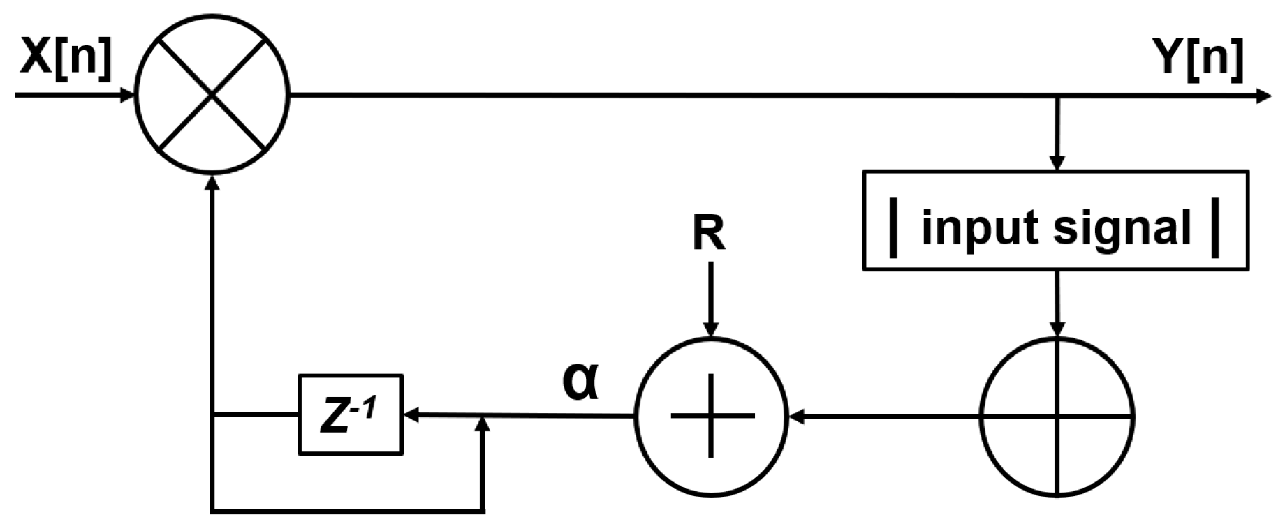
Figure 9 shows a simplified schematic of the proposed digital AGC. Unlike
Figure 2, the loop function is removed, and the power detector is simplified in such a way that the multiplier disappears and the absolute value is used.
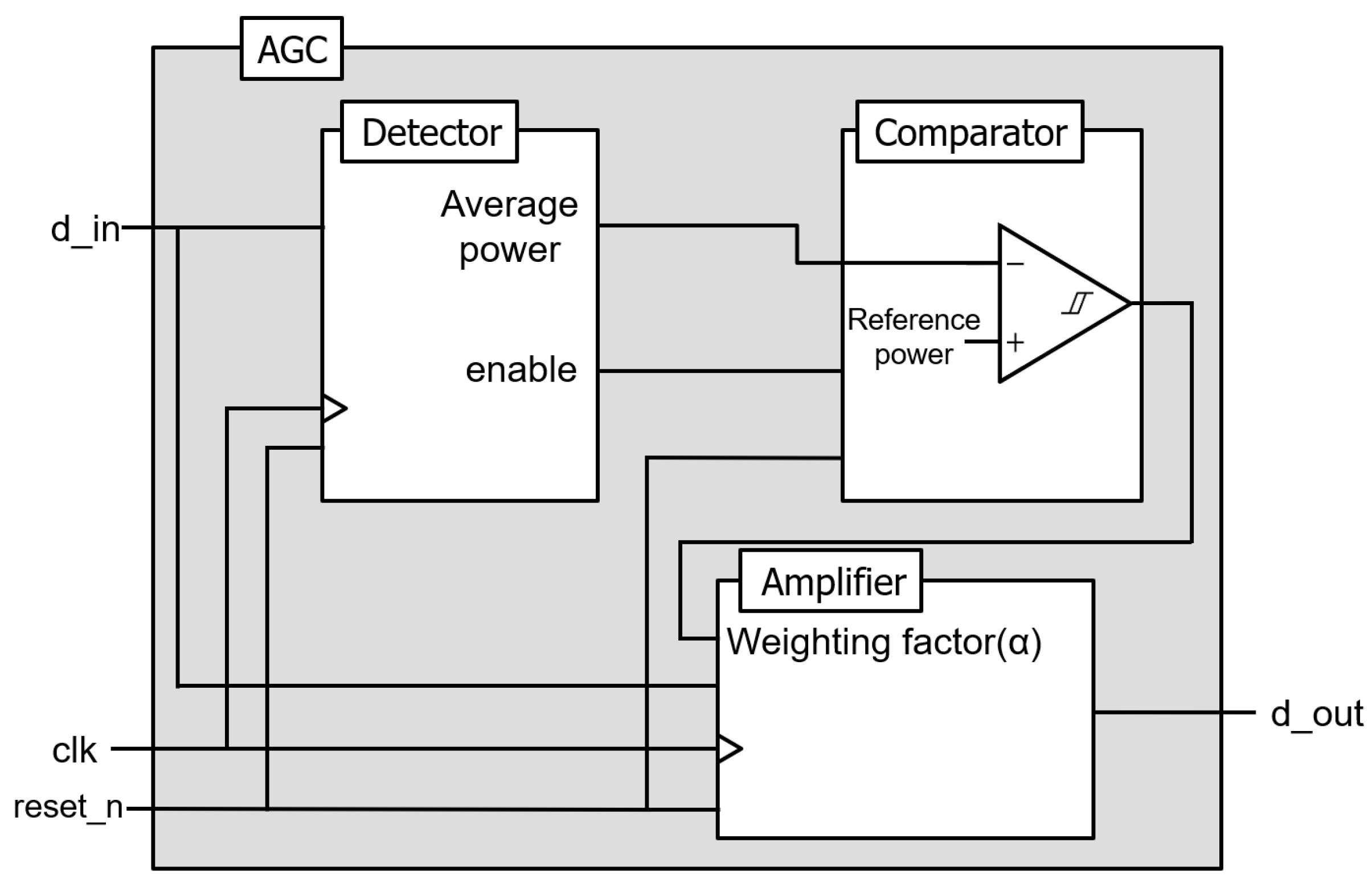
In this study, the digital AGC designed in FPGA consists of three modules, as shown in
Figure 10: a detector, a comparator, and an amplifier. First, the detector plays a role of measuring the power of the input signal (d_in). The detector receives the input signal during the specified window size and measures the average power. In general, the formula for measuring the average power is defined as follows:
Calculation of the average power of the input signal in a specific window size can be simplified as follows:
Then, the measured average power is compared with the reference power set by the user in the comparator to determine whether the input signal should be amplified or reduced. A weighting factor to multiply with the input signal can be calculated as follows:
If the measured average power is greater than the reference power, the weighting factor is less than 1. On the other hand, if the measured average power is lower than the reference power, the weighting factor is greater than 1. The amplifier amplifies and reduces the actual input signal based on the weighting factor calculated from the comparator, and outputs the modified signal (d_out).
In addition, a fixed-point multiplication method is used in the proposed AGC, which can perform both amplification and attenuation of the FM/T-DMB signals, different from the analog operational amplifier.
Simulations were conducted to verify the AGC operation, as shown in
Figure 11. As shown, signals of higher power and signals of lower power than the reference power level were attenuated and amplified, respectively, to become around 73 dB.
Table 8 shows the performance comparison between the proposed AGC and the AGC in Reference [
25]. As shown, with the proposed AGC, the maximum operating frequency was 2.5 times faster than the conventional AGC, the DSP slice was reduced to half, and the AGC is more versatile (i.e., can be used both for FM and DMB). In addition, the proposed repeater improves user convenience by allowing users to set as much gain as desired.
4. Experiment Result
We designed digital-signal-processing algorithms explained in the previous sections with Verilog Hardware Description Language (HDL) and implemented the whole repeater system to work for multichannel FM and T-DMB signals using FPGA. Xilinx Vivado version 17.4 was used to design Verilog HDL. In the experiment, we used the Xilinx Kintex 7 xc7k325tffg676-1 as the target FPGA board. We also used the AD9643BCPZ ADC to convert analog signals to digital signals. The ADC could generate a 14 bigs digital signal from analog input. It has a 1.75 V peak to peak full-scale input range, and the FM and DMB signals could be digitized by a single ADC. It operates up to 250 MSPS (million samples per second) [
31]. The AD9788BSVZ DAC was used to convert the output of the repeater back into an analog signal. It is a 16-bit high dynamic-range device that provides a sample rate of 800 MSPS. It can operate from 1.8 to 3.3 V supplies [
32]. In order to test the designed repeater, FM and DMB input signals were generated by using a function generator. A spectrum analyzer was used to measure the output signals to check the functionality of the proposed repeater. The block diagram of the designed digital-signal-processing unit is shown in
Figure 12.
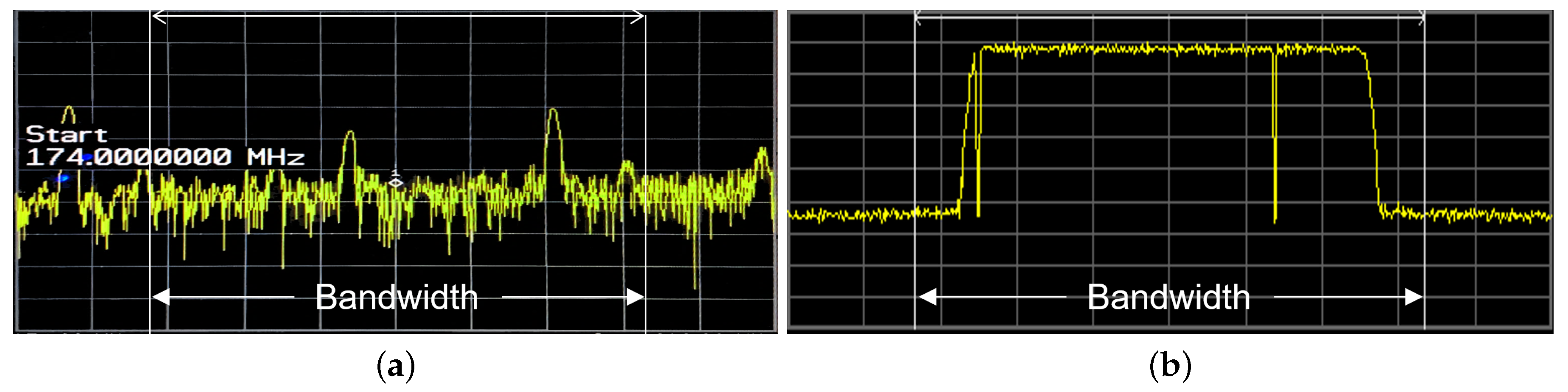
An experiment was conducted to verify the two main goals of the study. At first, the repeater has to precisely filter the adjacent channels to accurately operate for a total of 46 channels (40 FM and 6 DMB signals) at the same time. Second, the repeater should automatically maintain a constant output power level regardless of input power levels.
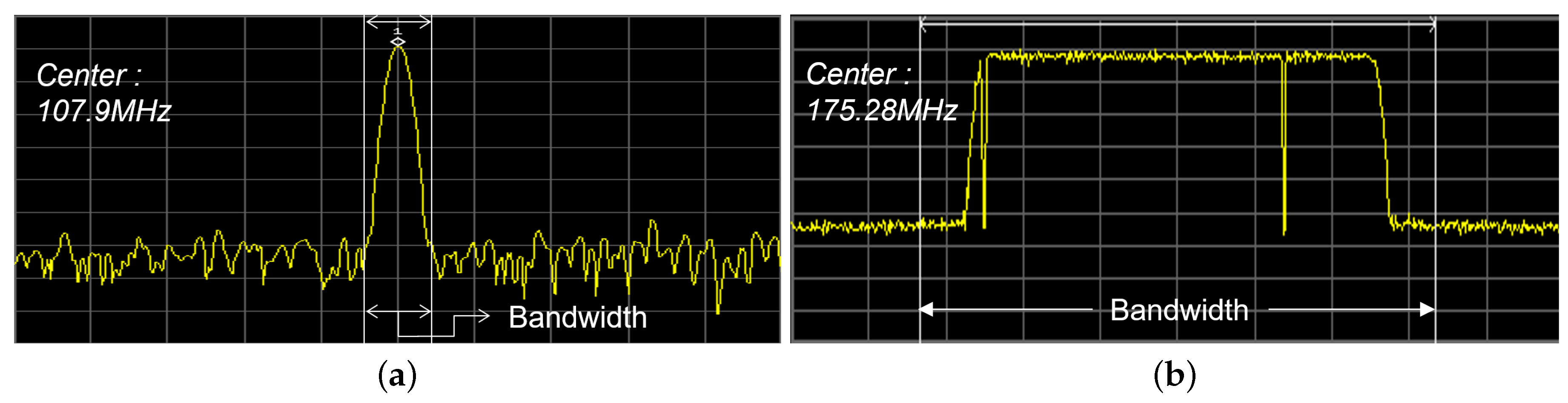
Single-channel simulation results are shown in
Figure 13. As shown, both the FM signal and the DMB signal were precisely removed from the adjacent frequency through the respective digital-signal-processing algorithms, maintaining at the desired power level.
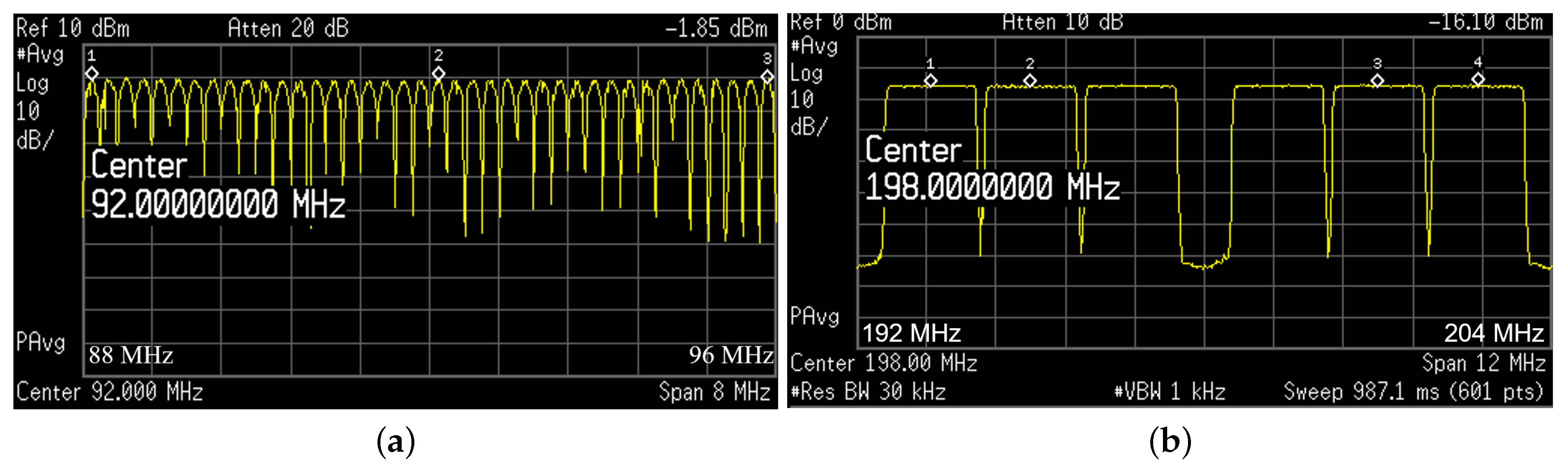
A multichannel simulation result for FM is shown in
Figure 14a. As shown, a total of 40 FM channels were controlled simultaneously so that the center frequency was precisely filtered without affecting adjacent channels. In addition, the power levels of all 40 channels from 88 to 96 MHz were precisely controlled. A multichannel simulation result for DMB is shown in
Figure 14b. As shown, a total of 6 DMB channels were correctly filtered simultaneously, and all power levels were maintained.
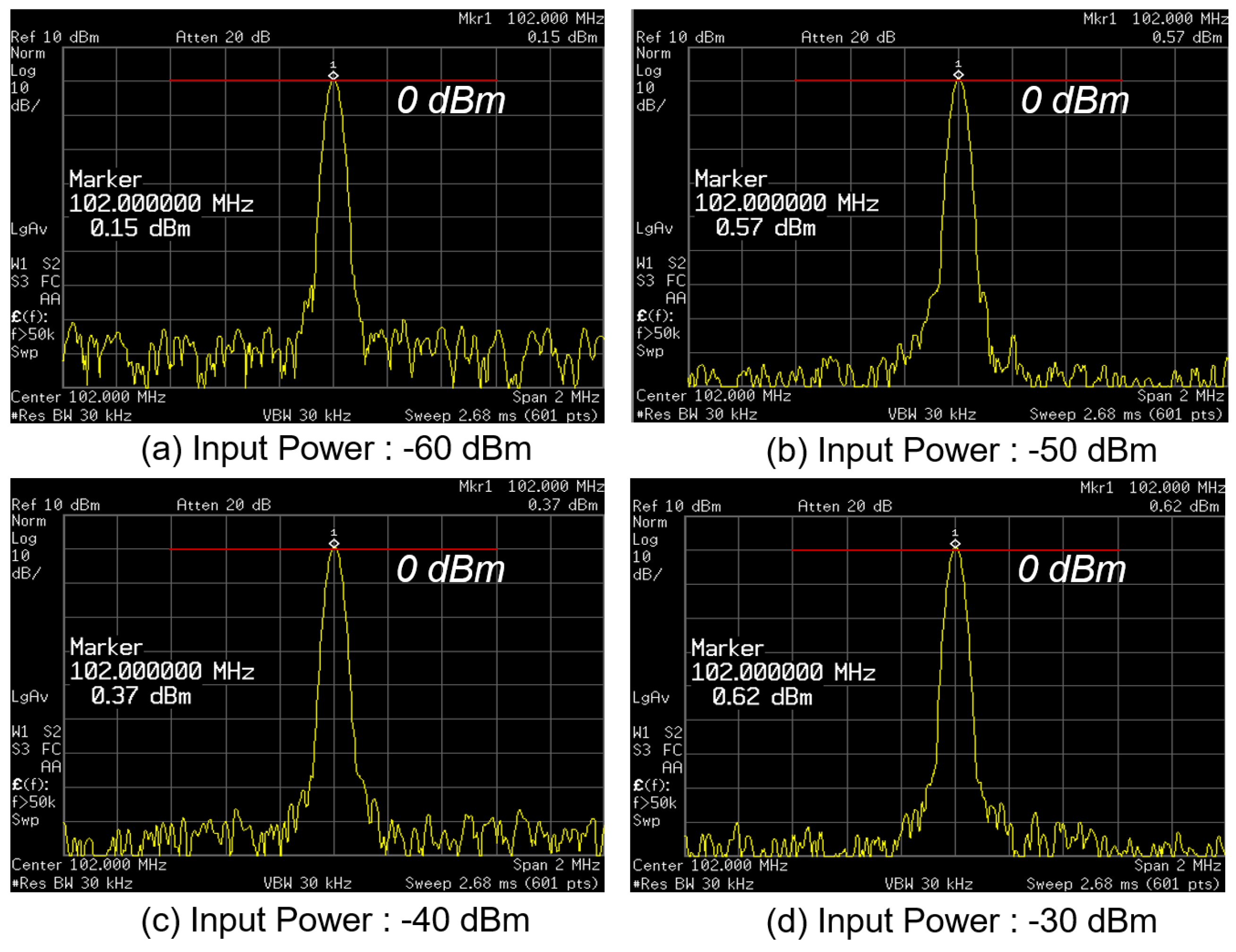
Figure 15 and
Figure 16 show the AGC operation of the FM signals and DMB signals, respectively. As shown in both figures, when signals of different power levels (e.g., −60, −50, −40, and −30 dBm) were applied, output power levels were constantly maintained at around 0 dBm.
In conclusion, it can be seen that 40 FM channels and 6 DMB channels were precisely controlled by accurately filtering adjacent channels and power levels were compensated correctly by the AGC.
Table 9 shows the comparison with existing FPGA-based repeaters for the FM signal. As shown, existing repeaters use an average of about 7 DSP slices in handling one channel. However, the proposed repeater designed in this study uses 5 DSP slices per channel and shows a much higher output sample rate. The proposed repeater can also operate up to 40 FM channels (with 6 DMB channels) at the same time. We prove that the proposed repeater is a more powerful repeater because it can operate not only FM 40 channel but also DMB 6 channel at the same time. In addition, the proposed AGC operates correctly, while the use of the DSP slice is reduced by 50%, and throughput is increased by 2.5 times, which is better than a conventional AGC.


