A 3GS/s 12-bit Current-Steering Digital-to-Analog Converter (DAC) in 55 nm CMOS Technology

 , ,
, ,
Abstract
:1. Introduction
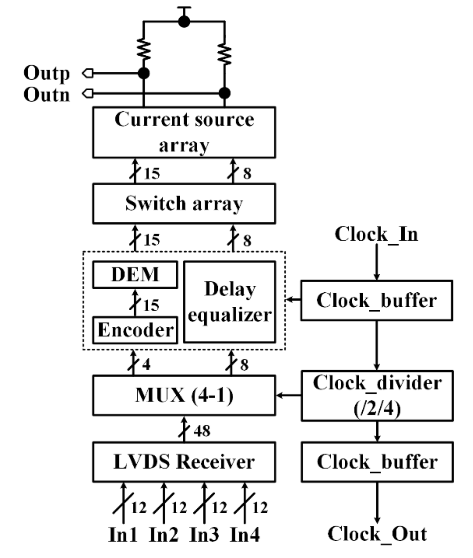
2. Proposed DAC Architecture
3. Circuits Implementation Details
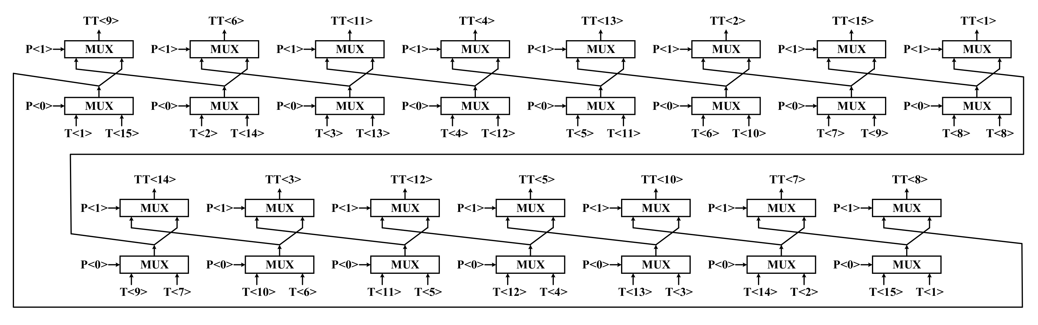
3.1. Partial Randomization Dynamic Element Matching Based on Switching Sequence Optimization
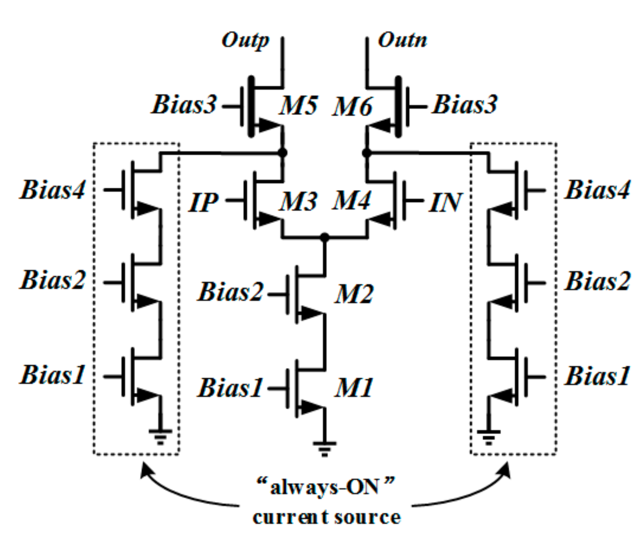
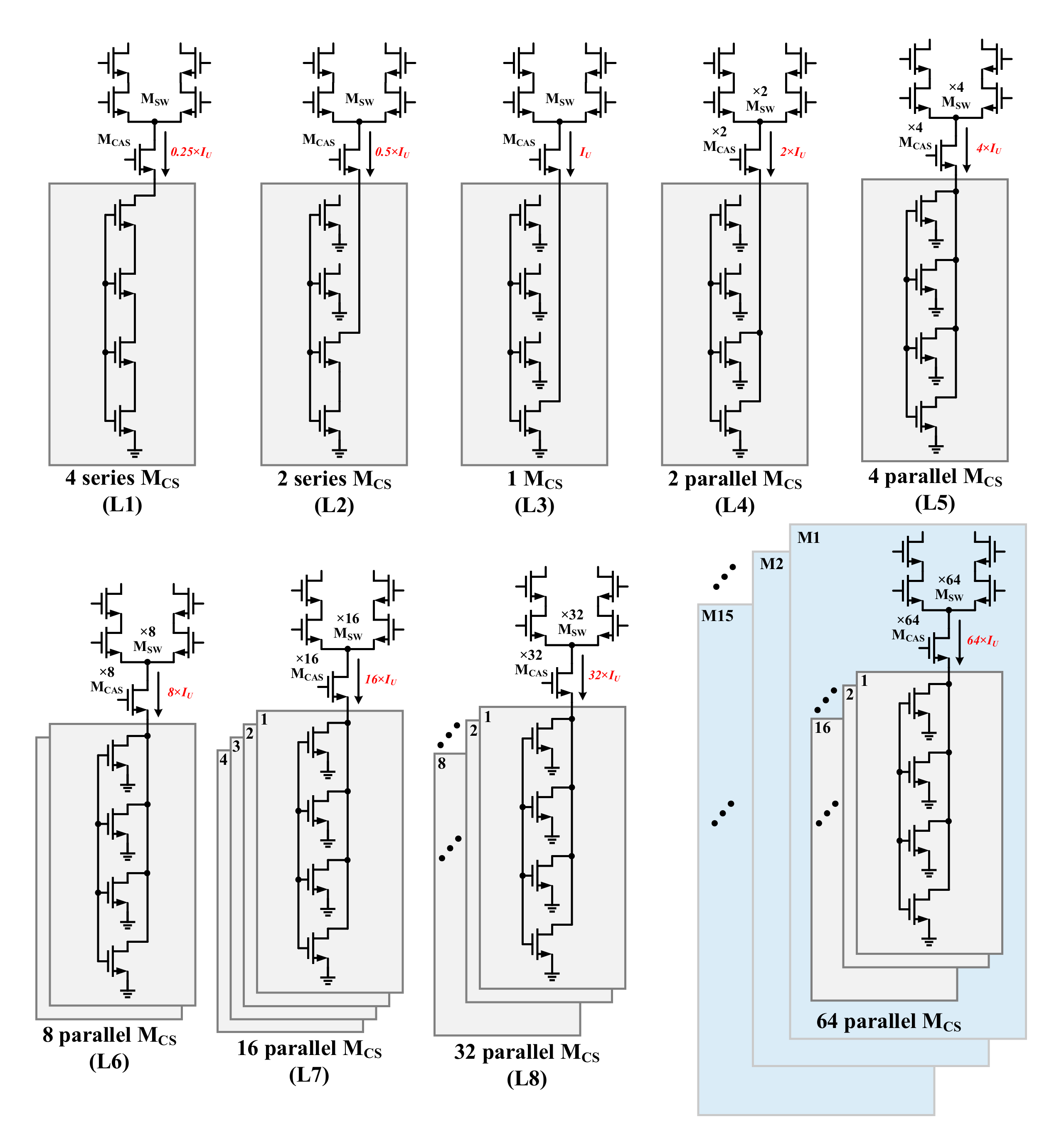
3.2. Switching Current Cell Design
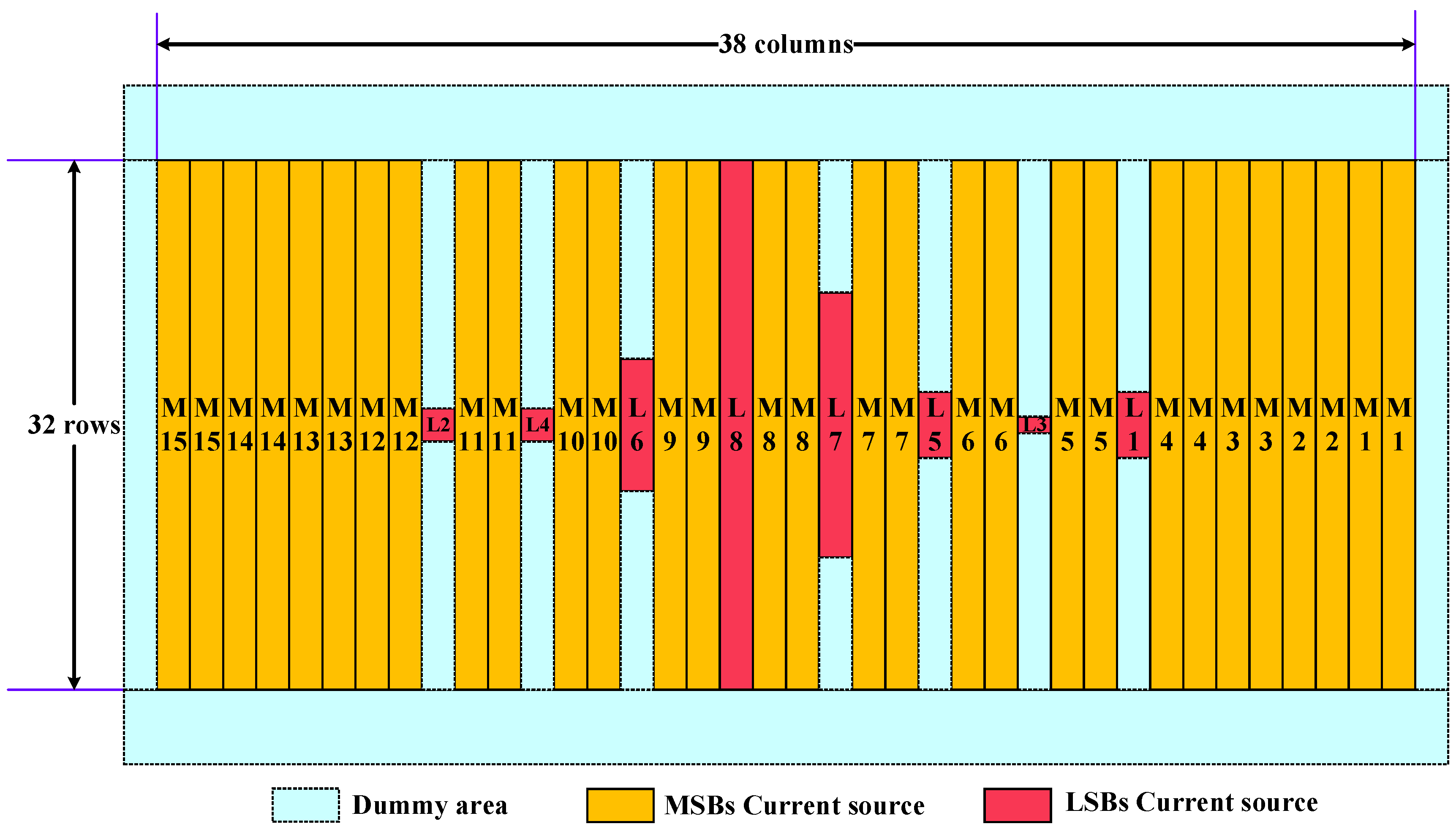
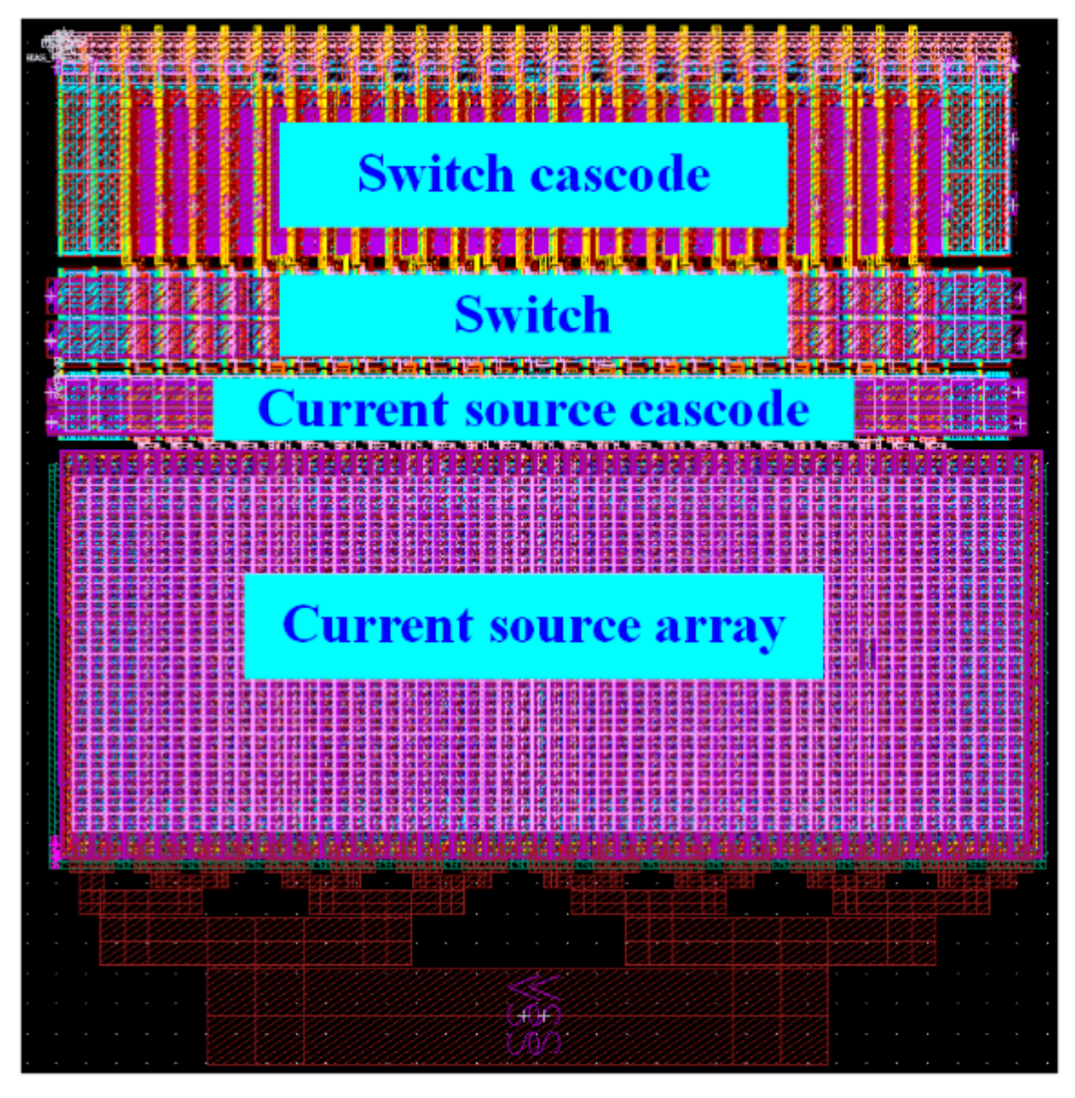
3.3. Switching Current Array Layout
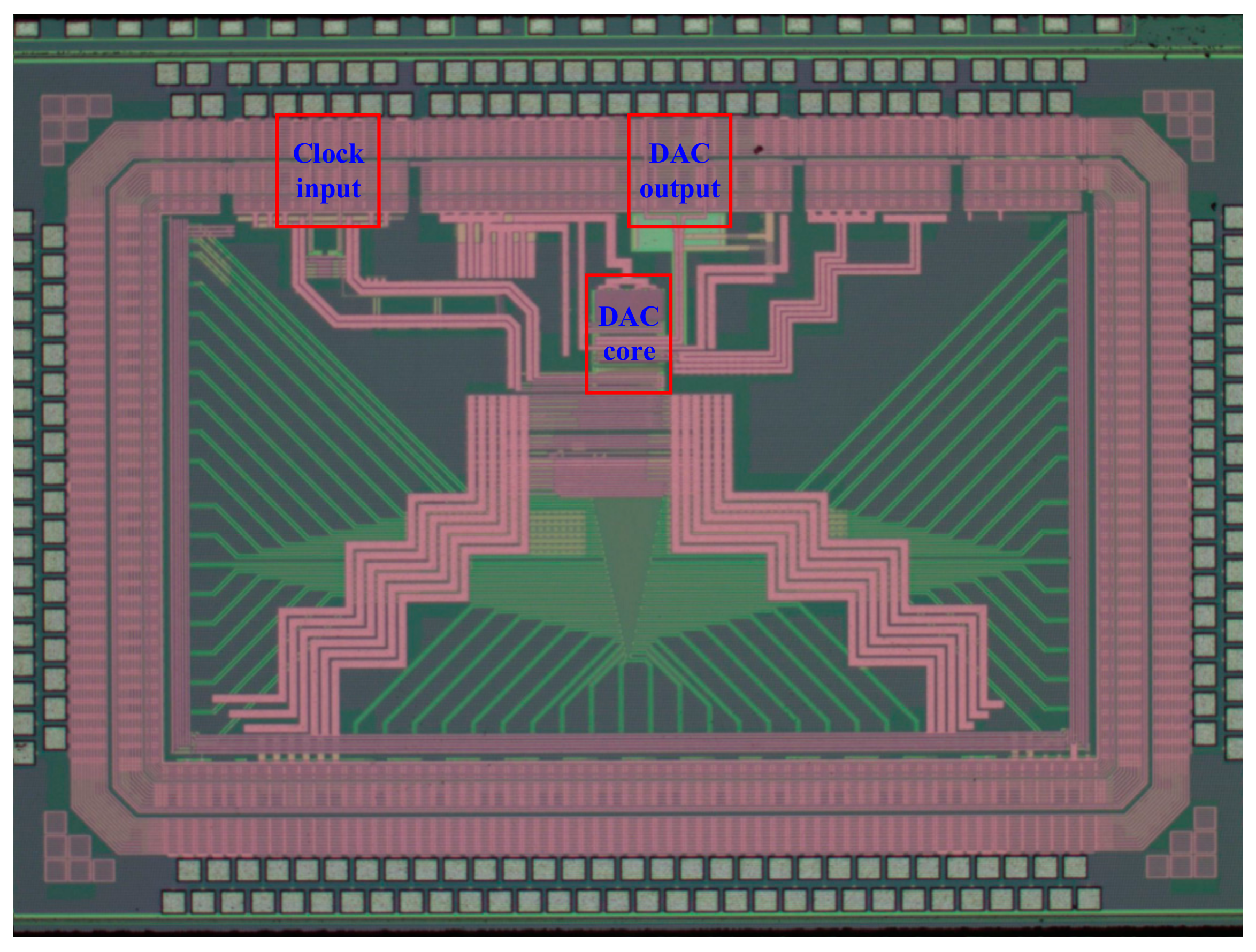
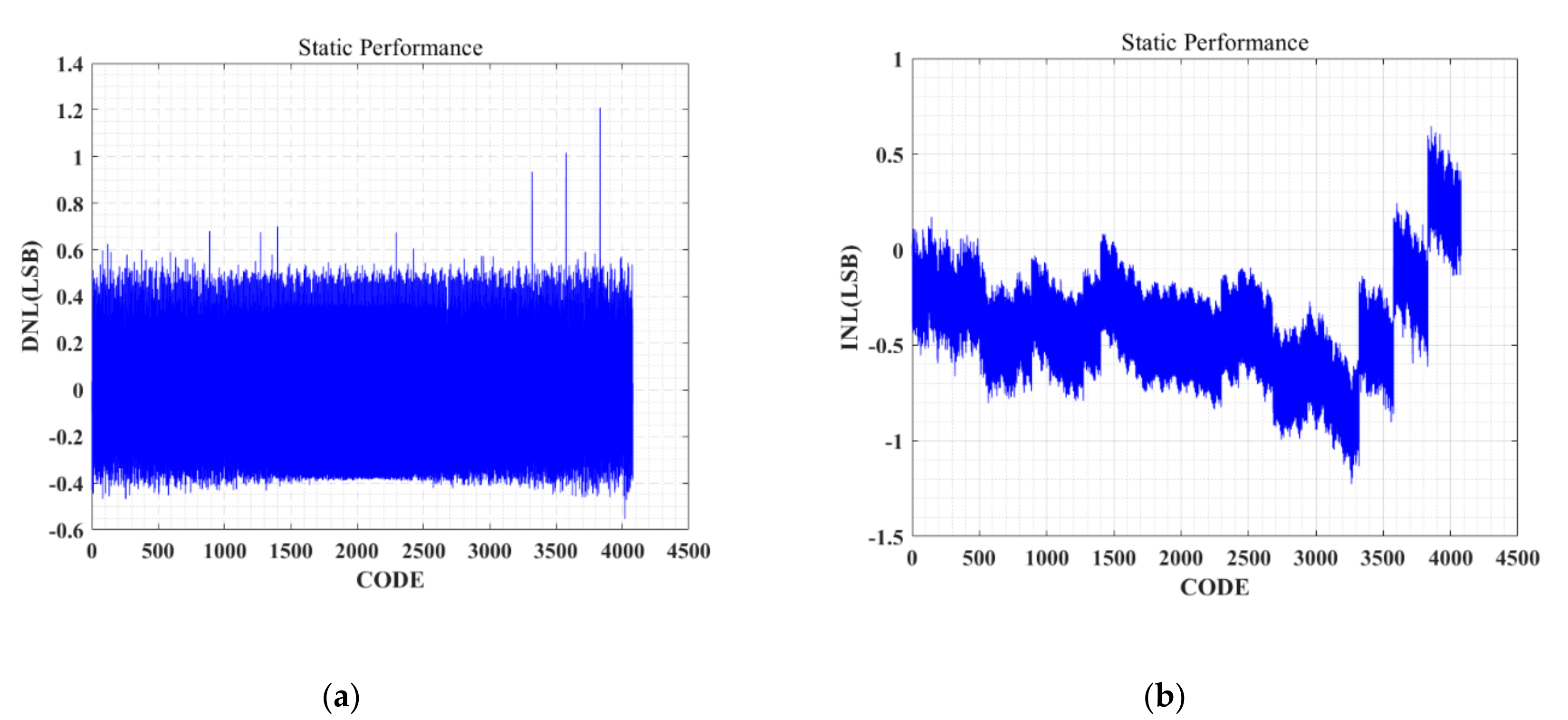
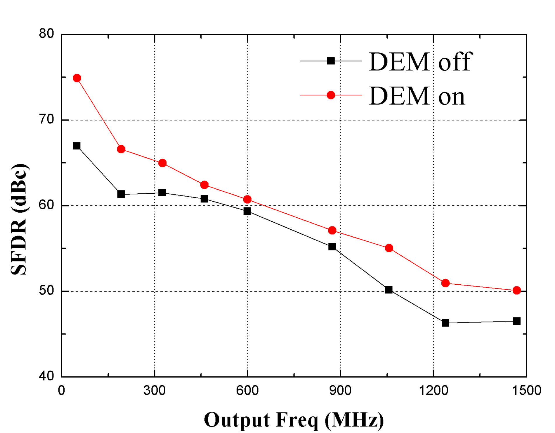
4. Measured Results
5. Conclusions
Author Contributions
Funding
Conflicts of Interest
References
- Ravinuthula, V.; Bright, W.; Weaver, M.; Maclean, K.; Kaylor, S.; Balasubramanian, S.; Coulon, J.; Keller, R.; Nguyen, B.; Dwobeng, E. A 14-bit 89 GS/s RF DAC in 40 nm CMOS achieving >71 dBc LTE ACPR at 2.9 GHz. In Proceedings of the 2016 IEEE Symposium on VLSI Circuits (VLSI-Circuits), Honolulu, HI, USA, 15–17 June 2016. [Google Scholar]
- Van de Sande, F.; Lugil, N.; Demarsin, F.; Hendrix, Z.; Andries, A.; Brandt, P.; Anklam, W.; Patterson, J.S.; Miller, B.; Rytting, M.; et al. A 7.2 GSa/s, 14 Bit or 12 GSa/s, 12 Bit Signal Generator on a Chip in a 165 GHz fT BiCMOS Process. IEEE J. Solid-State Circuits 2012, 47, 1003–1012. [Google Scholar] [CrossRef]
- Engel, G.; Kuo, S.; Rose, S. A 14b 3/6 GHz current-steering RF DAC in 0.18 μm CMOS with 66 dB ACLR at 2.9 GHz. In Proceedings of the 2012 IEEE International Solid-State Circuits Conference, San Francisco, CA, USA, 19–23 February 2012. [Google Scholar]
- Lin, C.; Wong, K.L.J.; Kim, T.-Y.; Xie, G.R.; Major, D.; Unruh, G.; Dommaraju, S.R.; Eberhart, H.; Venes, A. A 16b 6 GS/S nyquist DAC with IMD <−9 GHz in 16 nm CMOS. In Proceedings of the 2018 IEEE International Solid-State Circuits Conference (ISSCC), San Francisco, CA, USA, 11–15 February 2018. [Google Scholar]
- Engel, G.; Clara, M.; Zhu, H.; Wilkins, P. A 16-bit 10Gsps current steering RF DAC in 65 nm CMOS achieving 65 dBc ACLR multi-carrier performance at 4.5 GHz Fout. In Proceedings of the 2015 Symposium on VLSI Circuits (VLSI Circuits), Kyoto, Japan, 17–19 June 2015. [Google Scholar]
- Tseng, W.; Fan, C.; Wu, J. A 12-Bit 1.25-GS/s DAC in 90 nm CMOS With >70 dB SFDR up to 500 MHz. IEEE J. Solid-State Circuits 2011, 46, 2845–2856. [Google Scholar] [CrossRef]
- Lin, W.; Kuo, T. A 12b 1.6 GS/s 40 mW DAC in 40nm CMOS with >70 dB SFDR over entire Nyquist bandwidth. In Proceedings of the 2013 IEEE International Solid-State Circuits Conference Digest of Technical Papers, San Francisco, CA, USA, 17–21 February 2013. [Google Scholar]
- Lin, W.; Huang, H.-Y.; Kuo, T.-H. A 12-bit 40 nm DAC Achieving SFDR >70 dB at 1.6 GS/s and IMD <−61 dB at 2.8 GS/s With DEMDRZ Technique. IEEE J. Solid-State Circuits 2014, 49, 708–717. [Google Scholar] [CrossRef]
- Liu, M.; Zhu, Z.; Yang, Y. A High-SFDR 14-bit 500 MS/s Current-Steering D/A Converter in 0.18 µm CMOS. IEEE Trans. Very Large Scale Integr. VLSI Syst. 2015, 23, 3148–3152. [Google Scholar] [CrossRef]
- Lin, C.; van der Goes, F.; Westra, J.; Mulder, J.; Lin, Y.; Arslan, E.; Ayranci, E.; Liu, X.; Bult, K. A 12 bit 2.9 GS/s DAC With IM3 <−60 dBc Beyond 1 GHz in 65 nm CMOS. IEEE J. Solid-State Circuits 2009, 44, 3285–3293. [Google Scholar] [CrossRef]
- Wu, X.; Palmers, P.; Steyaert, M.S.J. A 130 nm CMOS 6-bit Full Nyquist 3 GS/s DAC. IEEE J. Solid-State Circuits 2008, 43, 2396–2403. [Google Scholar] [CrossRef]
- Tang, Y.; Van Beek, P.; Doris, K.; Briaire, J.; va Roermund, A.; Van Veldhoven, R. A 14 bit 200 MS/s DAC With SFDR >78 dBc, IM3 <−83 dBc and NSD <−163 dBm/Hz Across the Whole Nyquist Band Enabled by Dynamic-Mismatch Mapping. IEEE J. Solid-State Circuits 2011, 46, 1371–1381. [Google Scholar] [CrossRef]
- Kuo, K.-C.; Wu, C.-W. Digital to analog converter for the analog front end of the WiMAX applications. In Proceedings of the 2010 10th International Symposium on Communications and Information Technologies, Tokyo, Japan, 26–29 October 2010. [Google Scholar]
- Lin, W.-T.; Kuo, T.-H. A Compact Dynamic-Performance-Improved Current-Steering DAC With Random Rotation-Based Binary-Weighted Selection. IEEE J. Solid-State Circuits 2012, 47, 444–453. [Google Scholar] [CrossRef]
- Zhou, L.; Wu, D.; Jiang, F.; Wu, J.; Jin, Z.; Liu, X. A 2 GSps 12 bit DAC with SFDR >57.5 dBc up to Nyquist bandwidth. In Proceedings of the 2013 IEEE Bipolar/BiCMOS Circuits and Technology Meeting (BCTM), Bordeaux, France, 30 September–3 October 2013. [Google Scholar]
- Cong, Y.; Geiger, R.L. Switching sequence optimization for gradient error compensation in thermometer-decoded DAC arrays. IEEE Trans. Circuits Syst. II Analog Digital Signal Process. 2000, 47, 585–595. [Google Scholar]
- Kuo, K.-C.; Wu, C.-W. A Switching Sequence for Linear Gradient Error Compensation in the DAC Design. IEEE Trans. Circuits Syst. Express Briefs 2011, 58, 502–506. [Google Scholar] [CrossRef]
- Aluthwala, P.D.; Weste, N.; Adams, A.; Lehmann, T.; Parameswaran, S. Partial Dynamic Element Matching Technique for Digital-to-Analog Converters Used for Digital Harmonic-Cancelling Sine-Wave Synthesis. IEEE Trans. Circuits Syst. Regul. Pap. 2017, 64, 296–309. [Google Scholar] [CrossRef]
- Andersson, N.U.; Wikner, J.J. A strategy for implementing dynamic element matching in current-steering DACs. In Proceedings of the 2000 Southwest Symposium on Mixed-Signal Design (Cat. No. 00EX390), San Diego, CA, USA, 27–29 February 2000. [Google Scholar]
- Jensen, H.T.; Galton, I. An analysis of the partial randomization dynamic element matching technique. IEEE Trans. Circuits Syst. II Analog Digital Signal Process. 1998, 45, 1538–1549. [Google Scholar] [CrossRef]
- Jensen, H.T.; Galton, I. A low-complexity dynamic element matching DAC for direct digital synthesis. IEEE Trans. Circuits Syst. II Analog Digital Signal Process. 1998, 45, 13–27. [Google Scholar] [CrossRef]
- Jensen, H.T.; Jensen, J.F. Dynamic element matching for highly linear digital-to-analog conversion. In Proceedings of the 1999 Third International Conference on Advanced A/D and D/A Conversion Techniques and their Applications (Conf. Publ. No. 466), Glasgow, UK, 27–28 July 1999. [Google Scholar]
- Galton, I. Why Dynamic-Element-Matching DACs Work. IEEE Trans. Circuits Syst. Express Briefs 2010, 57, 69–74. [Google Scholar] [CrossRef]
- Remple, J.; Galton, I. The Effects of Inter-Symbol Interference in Dynamic Element Matching DACs. IEEE Trans. Circuits Syst. Regul. Pap. 2017, 64, 14–23. [Google Scholar] [CrossRef]
- Chan, K.L.; Rakuljic, N.; Galton, I. Segmented Dynamic Element Matching for High-Resolution Digital-to-Analog Conversion. IEEE Trans. Circuits Syst. Regul. Pap. 2008, 55, 3383–3392. [Google Scholar] [CrossRef]
- Chan, K.L.; Zhu, J.; Galton, I. Dynamic Element Matching to Prevent Nonlinear Distortion From Pulse-Shape Mismatches in High-Resolution DACs. IEEE J. Solid-State Circuits 2008, 43, 2067–2078. [Google Scholar] [CrossRef]
- Mao, W.; Li, Y.; Heng, C.-H.; Lian, Y. High Dynamic Performance Current-Steering DAC Design with Nested-Segment Structure. IEEE Trans. Very Large Scale Integr. VLSI Syst. 2018, 26, 995–999. [Google Scholar] [CrossRef]
- Kim, S.-N.; Kim, M.-R.; Sung, B.-R.-S.; Kang, H.-W.; Cho, M.-H.; Ryu, S.-T. A SUC-Based Full-Binary 6-bit 3.1-GS/s 17.7-mW Current-Steering DAC in 0.038 mm2. IEEE Trans. Very Large Scale Integr. VLSI Syst. 2016, 24, 794–798. [Google Scholar] [CrossRef]
- Van de Vel, H.; Briaire, J.; Bastiaansen, C.; van Beek, P.; Geelen, G.; Gunnink, H.; Jin, Y.; Kaba, M.; Luo, K.; Paulus, E.; et al. 11.7 A 240 mW 16b 3.2 GS/s DAC in 65 nm CMOS with <−80 dBc IM3 up to 600 MHz. In Proceedings of the 2014 IEEE International Solid-State Circuits Conference Digest of Technical Papers (ISSCC), San Francisco, CA, USA, 9–13 February 2014. [Google Scholar]
- Chang, L.; Ding, K.; Xu, Z.; Song, C.; Li, J.; Zou, D. A 2 GS/s 14-bit current-steering DAC in 65 nm CMOS technology for wireless transmitter. IEICE Electron. Express 2018, 15, 1–11. [Google Scholar] [CrossRef]


| Switching Sequence | INL * | Variance | |
|---|---|---|---|
| Sequential sequence | 1, 2, 3, 4, 5, 6, 7, 8, 9, 10, 11, 12, 13, 14, 15 | 28 | 421.86 |
| Symmetrical sequence | 13, 11, 9, 7, 5, 3, 1, 15, 2, 4, 6, 8, 10, 12, 14 | 7 | 9.33 |
| Optimized sequence (4 groups) | 8, 6, 10, 4, 12, 2, 14, 15, 1, 13, 3, 11, 5, 9, 7 | 4 | 4.8 |
| 7, 9, 5, 11, 3, 13, 1, 15, 14, 2, 12, 4, 10, 6, 8 | |||
| 8, 10, 6, 12, 4, 14, 2, 1, 15, 3, 13, 5, 11, 7, 9 | |||
| 9, 7, 11, 5, 13, 3, 15, 1, 2, 14, 4, 12, 6, 10, 8 |
| 2009 JSSC [10] | 2014 JSSC [8] | 2014 ISSCC [29] | 2018 IEICE [30] | This Work | |
|---|---|---|---|---|---|
| Technology | 65 nm | 40 nm | 65 nm | 65 nm | 55 nm |
| Sample Rate (GS/s) | 2.9 | 1.6/2.8 | 3.2 | 2 | 3 |
| Resolution (bits) | 12 | 12 | 16 | 14 | 12 |
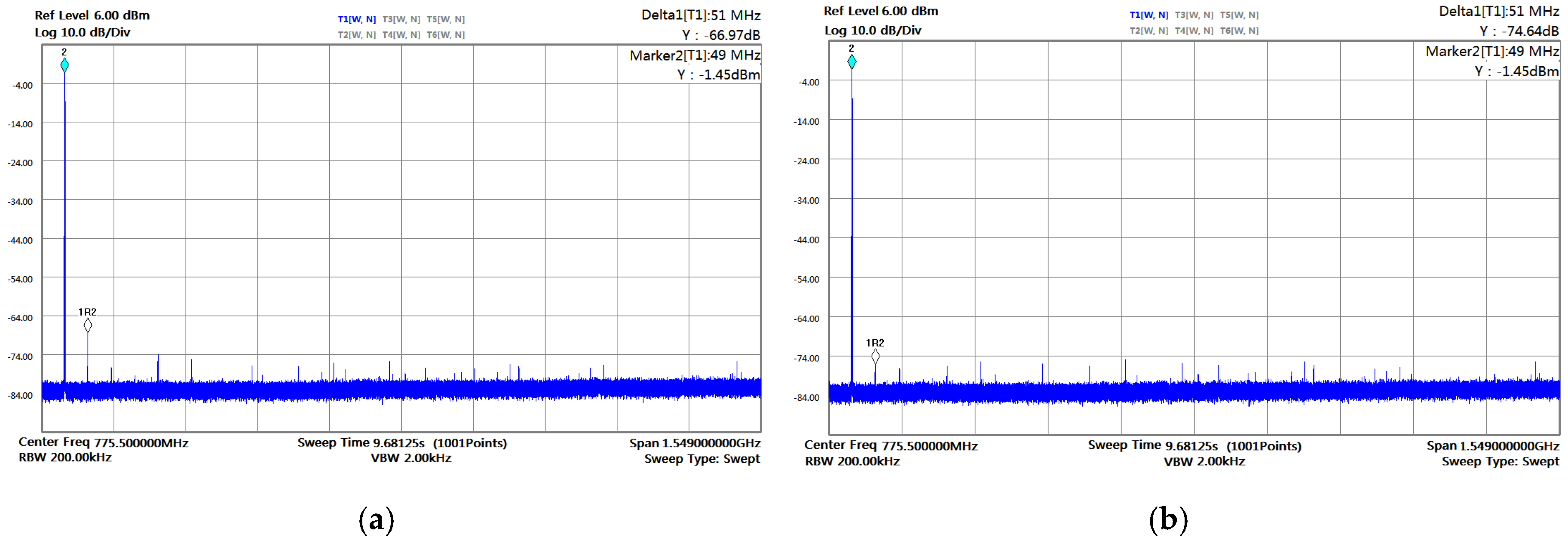
| Best SFDR (dBc) at low frequency | 74 | 74/58 | 84 | 78.2 | 74.64 |
| SFDR (dBc) at high frequency | 50 at 650 MHz | 70.3 at 0.8 GHz 48 at 1.4 GHz | 58 at 600 MHz | 53 at 310 MHz | 50 at 1 GHz |
| DNL/INL (LSB) | 0.3/0.5 | N/A | N/A | N/A | 1.21/1.22 |
| Power consumption (mW) | 188 | 40/47 | 240 | 490 | Total: 495 Core: 284 |
© 2019 by the authors. Licensee MDPI, Basel, Switzerland. This article is an open access article distributed under the terms and conditions of the Creative Commons Attribution (CC BY) license (http://creativecommons.org/licenses/by/4.0/).
Share and Cite
Wang, D.; Guo, X.; Zhou, L.; Wu, D.; Luan, J.; Liu, H.; Wu, J.; Liu, X. A 3GS/s 12-bit Current-Steering Digital-to-Analog Converter (DAC) in 55 nm CMOS Technology. Electronics 2019, 8, 464. https://doi.org/10.3390/electronics8040464
Wang D, Guo X, Zhou L, Wu D, Luan J, Liu H, Wu J, Liu X. A 3GS/s 12-bit Current-Steering Digital-to-Analog Converter (DAC) in 55 nm CMOS Technology. Electronics. 2019; 8(4):464. https://doi.org/10.3390/electronics8040464
Chicago/Turabian StyleWang, Dong, Xuan Guo, Lei Zhou, Danyu Wu, Jian Luan, Huasen Liu, Jin Wu, and Xinyu Liu. 2019. "A 3GS/s 12-bit Current-Steering Digital-to-Analog Converter (DAC) in 55 nm CMOS Technology" Electronics 8, no. 4: 464. https://doi.org/10.3390/electronics8040464
APA StyleWang, D., Guo, X., Zhou, L., Wu, D., Luan, J., Liu, H., Wu, J., & Liu, X. (2019). A 3GS/s 12-bit Current-Steering Digital-to-Analog Converter (DAC) in 55 nm CMOS Technology. Electronics, 8(4), 464. https://doi.org/10.3390/electronics8040464