1. Introduction
The evolution of all-optical signal processing is increasing in demand towards the implantation of ultra-high-speed photonic networks, such as optical packet switching. The infrastructure and physical layer of such networks must be enhanced by a design that can terminate the bottleneck introduced by electronic devices and the imperfection of its functionalities. One of the components required for this realization is an all-optical logic gate. These gates can further provide advanced optical signal processing functionalities such as packet switching, optical signal regeneration, header addressing, encryption and decryption, data encoding, header recognition, parity checking, label swapping, wavelength conversion and header extraction.
In general, conventional designs for photonic logic gates are based upon nonlinear effects in optical fiber such as four wave mixing, Self-Phase Modulation (SPM), Cross-Phase Modulation (XPM), and cross gain modulation in semiconductor optical amplifiers (SOA) and highly nonlinear fiber (HNLF). These nonlinear effects exist mostly in SOA and HNLF, and can be used in many applications. Namely, the Kerr nonlinear effect is defined as the third order nonlinear effect, which occurs when the refractive index changes the optical power, hence results in other secondary nonlinear phenomena such as four wave mixing, cross gain modulation, SPM and XPM. These effects can be used to implement many applications such as wavelength conversion, packet header optical processing, optical solition propagation, and optical phase conjugation as studied in [
1,
2].
Furthermore, the aforementioned applications constitute a key feature for next generation transmission networks. Hence it can be based on fiber mediums that have highly efficient nonlinear effects. Also, reduced attenuation levels are mandatory to increase effective nonlinear interactions.
Now conventional solutions, in particular, SOA designs for all-optical logic gates design [
3,
4,
5,
6] generally result in poor optical signals due to the pattern effect. This distortion is mainly caused by the intrinsic slow gain recovery time of the SOA which results in limited values of data rates. In contrast, HNLF presents a promising alternative for SOA attributable to its highly nonlinear coefficient, tuneable zero dispersion at C and L bands, lower attenuation, low zero dispersion slope, and low splice loss to conventional single mode fibers [
7,
8].
Various studies have looked at the design of photonic logic gates based on HNLF. Further, work in [
9] presents an XOR gate design using polarization rotation effects. Also, work in [
10] proposes a logic gate based on the Kerr effect as well in an effort to overcome SOA-based gates. However, these schemes are limited to 10 Gbps and suffer from a high HNLF length of 2 km with low nonlinear coefficients. Moreover, work in [
11] leverages photonic crystals to present logic gates using a two-staged structure, i.e., a structure comprised of waveguides and ring resonators. However, the use of ring resonators imposes high control levels of the signal power because high light intensity is required for changing the refractive index of nonlinear materials here.
In light of the above, the work here aims to utilize HNLF for all-optical XOR photonic logic gates to overcome the deficiencies associated with SOA, i.e., enhanced power efficiency, and ring resonators. The simplified gate structure here (based on HNLF component only) achieves high data rates with a relatively high nonlinear coefficient, as compared to existing methods in [
9,
11]. Namely, a simplified XOR gate design is proposed based on a single stage HNLF. Also, the proposed design achieves high data rates (20 Gbps) with high extinction ratios. The HNLF performs the same logical operations as SOA by acting as a passive device, and hence utilizing low optical power levels. Furthermore, the proposed XOR configuration provides more flexibility to the optical transmission networks. Overall, HNLF-based gates have the potential of monolithic integration, offering advantages such as compactness, increased reliability, and cost reduction [
12].
This paper is organized as follows.
Section 2 presents the design concept for the proposed logic gate and the various components used in this design along with the signal flow sequence at each stage. Then, the HNLF output and the BPF calibration settings are shown in
Section 3. The BPFs output results are presented in
Section 4. This is followed by simulation results and performance analysis in
Section 5, along with conclusions in
Section 6.
2. Design of XOR Photonic Logic Gate
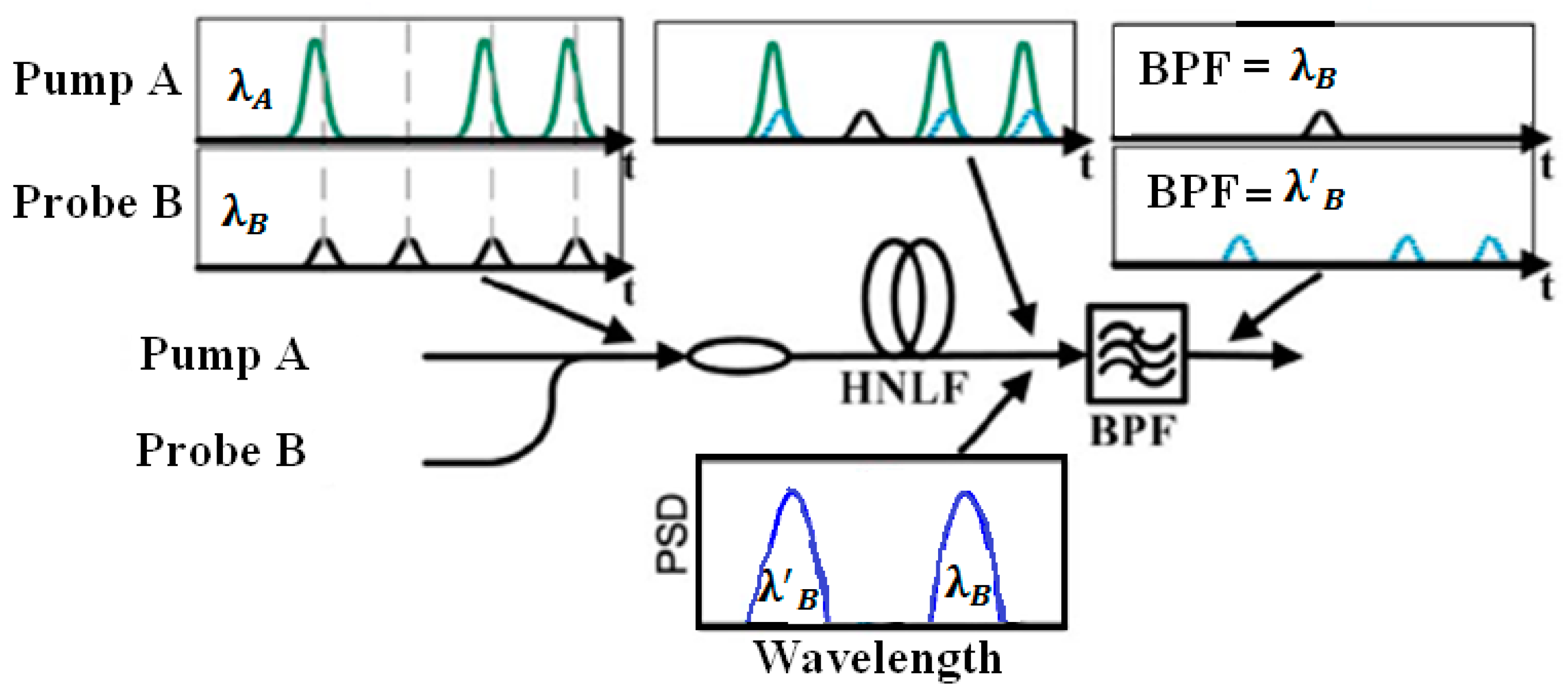
Consider two synchronized pulse light beam signals operating at 20 Gbps, aligned at two different wavelengths with a specific data modulation format which are injected into the highly nonlinear fiber, as conceptually depicted in
Figure 1. Both signals are within the same polarization states. A non-return to zero with on-off keying (NRZ-OOK) modulation format is selected here due to its constant power levels when transmitting an entire bit slot. This makes the NRZ modulation format a common choice for optical fiber communications systems, e.g., for metropolitan-area networks (MAN). As a result, the data is in NRZ-OOK format comprising picosecond full width half maximum (FWHM) pulse width. Because the duty cycle is very small, a reduced amount of average power is needed to generate significant and noticeable SPM-XPM idlers.
In order to increase the strength of the generated SPM-XPM idler, the lights are co-polarized with each other [
13]. Signal A here acts as a pump signal at an operating wavelength,
, while signal B acts as a probe signal at an operating wavelength,
. After propagating through the HNLF medium, the spectrum of probe B experiences an SPM and XPM induced frequency shift at
which is proportional to the slope of the power profile of the pump signal. At the output of the HNLF, the probe spectrum mainly contains two fundamental lobes [
14]:
One spectral lobe at , which is identical to the probe spectrum before the XPM which is formed by the logical zeros of pump A.
Second, the spectral lobe at , which is a spectrally shifted replica of the probe spectrum which is formed by the logical ones of pump A as illustrated at the output of the HNLF.
The resultant idlers generated by the SPM and XPM will act as the photonic XOR gate of the two input signals. The actual logic gate output is acquired by spectrally filtering out one of the generated idler wavelengths. A band pass filter (BPF) can be employed to select the desired output spectrum in order to perform the logical operation of the gate.
The two optical pulses were generated by a user defined bit sequence generator (UDBSG) and an optical Gaussian pulse generator (OGPG). Polarization controllers were used to enhance synchronization between the signals. They were followed by isolators which reject the reflected light in the transmission path. Both sequences were then amplified by Erbium-doped fiber amplifiers (EDFA). Optical cross-connectors (XC) with different coupling coefficients acted as power splitters and combiners to generate the pump and probe signals with different optical power levels.
Furthermore, optical circulators (OCs) were used to ensure the injection of the propagated pump and probe into the HNLF. By adjusting the cut-off wavelength of the BPF, the desired optical logic gate could be generated as will be explained later. Also, variable optical attenuators (VOA) and optical delay lines (ODL) were used for synchronization purposes. Indeed, an optical receiver was used to measure the performance of the system using a certain analysis method by connecting eye pattern and bit error rate analyzers.
The propagation of the signals was monitored in the time domain using an optical time domain visualizer (OTDV) and in the frequency domain using an optical spectrum analyzer (OSA). The optical power was detected at each stage by an optical power meter (OPM).
Figure 2 shows the circuit diagram of the proposed XOR gate, composed of the various interconnected elements, in particular, the UDBSG, OGPG, EDFA, XC, OC, BPF, and VOA. The signal flow sequence is also shown in
Figure 2, including the output of the XC at each stage. Note that this design is simulated by the Optisystem software package (based on realistic photonic models) and that it was used for the physical layer implementation of various optical communication systems, such as long hauls, LANs, and MANs.
3. HNLP Output
Note that the main HNLF design parameters used in this design are as follows. The length is 1.007 km, the nonlinear coefficient is 12.5 1/W.km, the dispersion slope is 0.0074 ps/nm
2/km, and the scattering section dispersion is 100 m. The calibration of the BPF1 and BPF2 controls the output of the HNLF in order to achieve XOR operation. The output of the HNLF when using pump B, yields probe A to propagate via the optical circulator A, as an input to BPF1. Meanwhile, the output when using pump A, results in probe B to be directed towards OC B, and acts as an input to BPF2. In order to perform the photonic XOR logic gate at the output of the designed circuit, the values of the BPFs should be calibrated in a way that function
(pump A and probe B) is achieved after BPF1 and (
) is resultant after BPF2 (see
Table 1).
BPF outputs are coupled via the optical coupler which will result in the optical XOR logic gate for the input binary sequence of signals A and B. The adjustment of the BPFs conforms to the following criteria:
If the BPF keeps the original signal wavelength components at
and removes the wavelength spectral components that were generated by the XPM effect at
or
then the logical operation
is performed [
14]. The BPF1 input port is composed of an original probe A wavelength spectrum at
and the identical shifted XPM replica at
= 1558.08 nm. BPF1 will clip
As a result, the cut-off wavelength of BPF1 will be
= 1555.08 nm.
Figure 3 and
Figure 4 illustrate the time domain and spectral output of BPF1, respectively, i.e., composed of the filtered spectral component at 1555.08 nm with adjacent negligible low power side band around 1500–1530 nm. Furthermore, the optical power for the main output spectrum is recorded here as −11.151 dBm.
4. Band Pass Filter Stages for the XOR Gate
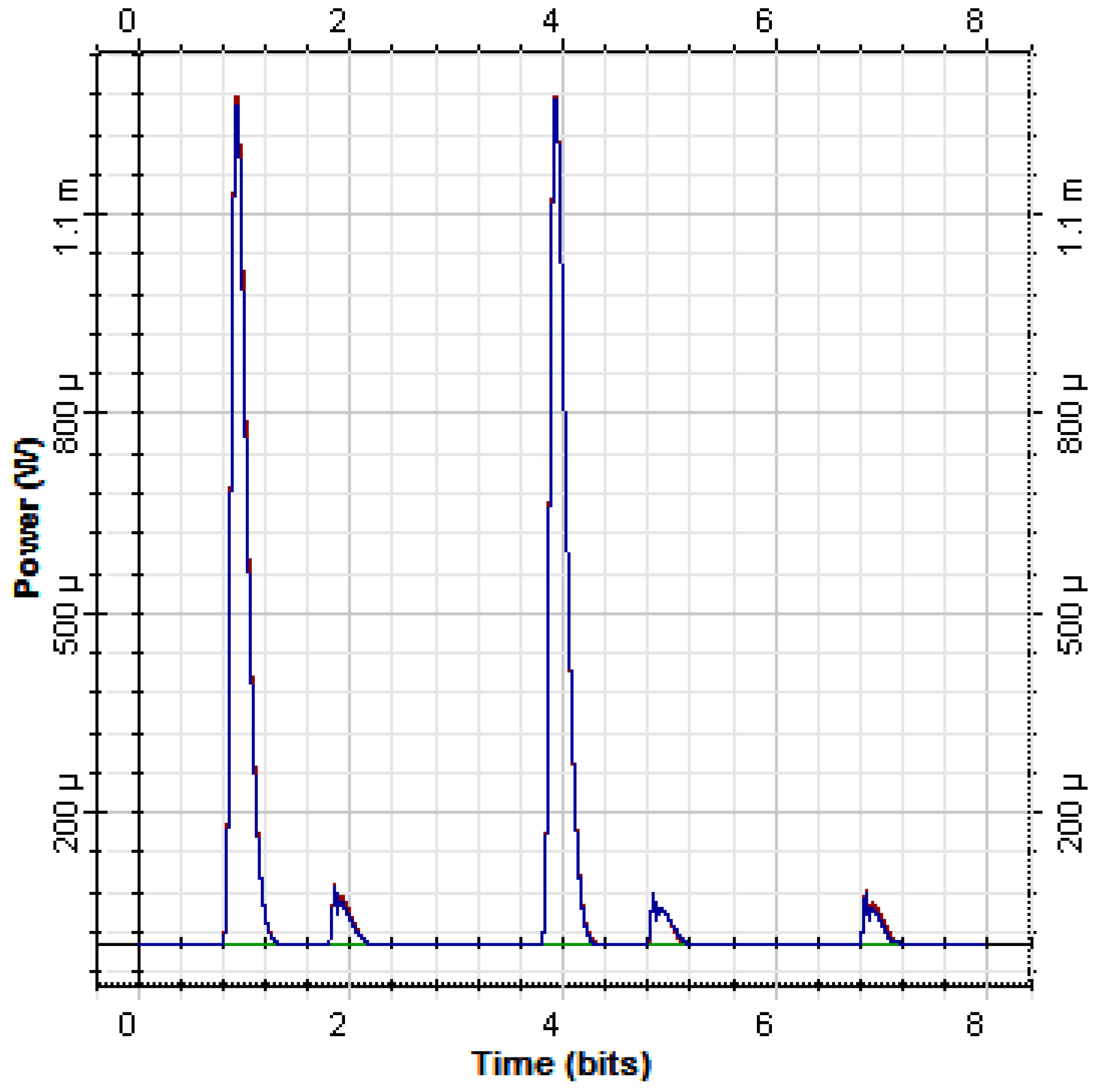
In the time domain, the output binary sequence after BPF1 is shown in
Figure 3 as 01001010 at P = 1.2 mw. This sequence is generated upon the convolution process between the input sequence to BPF1 (11011010) and the impulse response of the optical filter expressed by a ‘since’ function. This resulting BPF1 is to be coupled with BPF2 at later stages in order to generate the XOR gate). Similarly, a variable optical attenuator was connected after BPF1 to maintain the signal synchronization.
The BPF2 input port contains the original probe B wavelength spectrum at
and the identical shifted XPM replica at
= 1538.32 nm as shown in
Figure 4. BPF2 clips
. As a result, the cut-off wavelength of BPF1 will be selected as
= 1541.3 nm.
The optical time domain visualizer in
Figure 5 illustrates the binary output from the convolution between the impulse response of the filter and the binary sequence 01101010 (output of OC2). The resultant logic is 10010000 which is the second input arm required to generate the XOR gate by the optical coupler. The output spectrum is composed of the filtered spectra at
and the adjacent low power side band spectrum between 1550–1570 nm, as per
Figure 6. This is attributed to the available noise introduced by the EDFA amplifier in the earlier stage of the design. However, this side band have negligible effect to the performance of the logic gate due to the low power level compared to that of the main spectrum (−12.079 dBm), as gauged in
Figure 7.
Note that an optical delay line is adjusted after BPF2 in order to equalize the power values and optical pulses before the combination process.
For the output at the optical coupler stage, both branches which output from BPF1 and BPF2 are coupled together by employing a 50:50 coupler with coupling coefficient = 0.5. As a result, the XOR operation for the photonic logical gate is performed between the two binary sequences, as shown in
Figure 7 with a bit sequence of 11011010.
The optical spectrum analyzer in
Figure 8 shows the coupled wavelengths at 1541.3 nm and 1555.08 nm, respectively, which corresponds to the logical XOR operation of both input signals at −11.590 dBm as recorded from the OPM of the XOR gate.
5. Performance Analysis
At the optical coupler stage, the XOR photonic gate is launched at 20 Gbps with acceptable signal qualities in both the time and spectral domains. The output is then followed by the optical receiver for analytical processing by the eye pattern diagram and the BER analyzer in
Figure 9 and
Figure 10. Next, key physical-layer performance metrics are observed and calculated based upon prior observations in order to assess and characterize the optical signals generated.
The maximum quality factor (
Q-factor) of the oscillation as recorded from
Figure 10 is
Q = 25.9796, which shows reduced power and energy losses resulting in reduced damping rates. The eye amplitude indicates the level of distinction between logic 1 and logic 0 levels, which is determined as follows: level one − level zero = 225 − 17 = 208 (23.18063 dB), i.e., the work here shows a large difference between the logic 1 level and the logic 0 level histogram mean values of the plotted eye diagram. The extinction ratio between the two optical signal levels is determined as:
The recorded values here indicate a high quality generated optical signal. This value can significantly improve bit error ratio (BER) levels, as well as reduce the number of errors and the amount of error correction required. Furthermore, the opening eye factor is calculated as:
Moreover, a high opening eye factor is recorded. This indicates minimal signal distortion levels for the proposed XOR gate. The resultant signal therefore features low noise levels whereby the amplitude levels are sufficient to be distinguished as marks. In addition, the optical signal to noise ratio (OSNR) is also defined as:
This value suggests a reduced impairment degree at which the XOR optical signal is carried out in the HNLF medium and the induced optical amplifiers.
Figure 10 plots the
Q-factor against a one bit period, yielding a minimum BER of 3.20295 × 10
−149.
Note that the recorded BER value here indicates a minimum level of random noise, jitter, and other disturbances resulting in reduced bit errors. Finally, the quantitative power penalty required to compensate for propagation degradation and dispersion, thereby achieving comparable SNR (or BER) performance levels as compared to ideal system is calculated as:
Note that the proposed gate features a very low power penalty, i.e., power consumption levels, because it performs the required functionalities at very low input power values. Furthermore, the output power values can be amplified and improved if cascaded circuits were to be based on this design, such as optical sub-tractors.
Overall, the simulation results here show that the proposed XOR all-optical logic gate provides good performance using the HNLF implemented structure at 20 Gbps. Namely, the clear eye opening percentage = 80.28846% low BER, along with a small power penalty at −2.0568 dB and a high extinction ratio at 11.217336 dB. The results demonstrate a high level of distinction between logic zeros and ones at the receiver side due to the high extinction ratio.
6. Conclusions
In this paper, a novel architecture for a reconfigurable photonic XOR logic gate for 8 OOK-NRZ sequence bits is proposed. The design exploits SPM and XPM phenomena, leveraging the Kerr nonlinear effects in HNLF. The phenomena of SPM and XPM are captured in the effect of the spectral broadening toward blue and red spectral edges. The proposed HNLF-based design overcomes many of the challenges in conventionally implemented gate structures based on SOA designs. For the first time, those gates were realized at operating data rates of 20 Gbps and at high extinction ratios, a low BER, and low power penalty. Moreover, no additional input beams are required such as clock signals.
Future efforts may look into the design of the proposed gate using alternative modulation schemes, such as the non-return-to-zero polarization shift keying (NRZ-PolSK) as compared to NRZ-OOK. In this case, the design may feature light beams that propagate at different polarization modes and hence, gates can be generated by adjusting the relative polarization state between input signals. Furthermore, the proposed reconfigurable XOR photonic gate can be integrated into a cascaded design to launch optical flip flops using a set-rest (SR) latch based upon HNLF instead of SOA.
Author Contributions
Conceptualization, M.A.J. and A.A.; methodology, M.A.J. and A.A.; software, M.A.J.; validation, M.A.J. and A.A.; formal analysis, A.A.; investigation, M.A.J. and A.A.; resources, M.A.J. and A.A.; data curation, A.A.; writing—original draft preparation, M.A.J. and A.A.; writing—review and editing, A.A.; visualization, A.A.; supervision, M.A.J. A.A.; project administration, A.A.; funding acquisition, A.A.
Funding
This work is funded by Deanship of Scientific Research at King Faisal University, grant number 186005.
Conflicts of Interest
The authors declare no conflict of interest.
References
- Willner, A.E. All-optical signal processing techniques for flexible networks. In Proceedings of the Optical Fiber Communications Conference and Exposition (OFC), San Diego, CA, USA, 11–15 March 2018. [Google Scholar]
- Glesk, I.; Ahmed, M.; Wang, Z.; Chen, L.R. Towards integrated devices for ultrafast all-optical signal processing in optical networks. In Proceedings of the Smart Photonic and Optoelectronic Integrated Circuits, San Francisco, CA, USA, 29 January–1 February 2018. [Google Scholar]
- Li, P.-L.; Huang, D.-X.; Zhang, X.-L. SOA-Based Ultrafast Multifunctional All-Optical Logic Gates with PolSK Modulated Signals. IEEE J. Quantum Electron. 2009, 45, 1542–1550. [Google Scholar] [CrossRef]
- Houbavlis, T.; Zoiros, K.; Hatziefremidis, A.; Avramopoulos, H.; Occhi, L.; Guekos, G.; Hansmann, S.; Burkhard, H.; Dall’Ara, R. 10 Gbit/s all-optical Boolean XOR with SOA fibre sagnac gate. IET Electron. Lett. 1999, 35, 1650–1652. [Google Scholar] [CrossRef]
- Li, W.; Hu, H.; Zhang, X.; Dutta, N.K. High speed all optical logic gates using binary phase shift keyed signal based on QD-SOA. Int. J. High Speed Electron. Syst. 2015, 24, 1550005. [Google Scholar] [CrossRef]
- Hu, H.; Zhang, X.; Zhao, S.; Zhang, L. High-speed all-optical logic gate using QD-SOA and its application. Cogent Phys. 2017, 4. [Google Scholar] [CrossRef]
- Grüner-Nielsen, L.; Pálsdóttir, B. Highly nonlinear fibers for very wideband supercontinuum generation. Proc. SPIE 2008. [Google Scholar] [CrossRef]
- Liu, H.; Huang, Y.; Liu, D. Analysis and fabrication of highly nonlinear photonic crystal fiber. Proc. SPIE 2008. [Google Scholar] [CrossRef]
- Yu, C.; Christen, L.; Luo, T.; Wang, Y.; Pan, Z.; Yan, L.; Willner, A.E. All-optical XOR gate using polarization rotation in single highly nonlinear fiber. IEEE Photonics Technol. Lett. 2005, 17, 1232–1234. [Google Scholar] [CrossRef]
- Yu, C.; Christen, L.; Luo, T.; Wang, Y.; Pan, Z.; Yan, L.-S.; Willner, A.E. All-optical XOR gate based on Kerr effect in single highly-nonlinear fiber. In Proceedings of the Conference on Lasers and Electro-Optics, San Francisco, CA, USA, 16–21 May 2004. [Google Scholar]
- Salmanpour, A.; Mohammadnejad, S.; Bahrami, A. All-optical photonic crystal AND, XOR, and OR logic gates using nonlinear Kerr effect and ring resonators. J. Mod. Opt. Taylor Fr. 2015, 62, 693–700. [Google Scholar] [CrossRef]
- Li, Z.; Li, G. Ultrahigh-speed reconfigurable logic gates based on four-wave mixing in a semiconductor optical amplifier. IEEE Photonics Technol. Lett. 2006, 18, 1341–1343. [Google Scholar] [CrossRef]
- Fai, L.M. All-Optical Signal Processing Based on Optical Parametric Amplification. Ph.D. Thesis, University of Hong Kong, Hong Kong, China, 2008. [Google Scholar]
- Qiu, J.; Sun, K.; Rochette, M.; Chen, L. Reconfigurable all-optical multilogic gate based on cross-phase modulation in a highly nonlinear fiber. IEEE Photonics Technol. Lett. 2010, 22, 1199–1201. [Google Scholar] [CrossRef]
© 2019 by the authors. Licensee MDPI, Basel, Switzerland. This article is an open access article distributed under the terms and conditions of the Creative Commons Attribution (CC BY) license (http://creativecommons.org/licenses/by/4.0/).


