Communication

Effect of Top Channel Thickness in Near Infrared Organic Phototransistors with Conjugated Polymer Gate-Sensing Layers

1
Organic Nanoelectronics Laboratory, KNU Institute for Nanophotonics Applications (KINPA), Department of Chemical Engineering, School of Applied Chemical Engineering, Kyungpook National University, Daegu 41566, Korea
2
Priority Research Center, Research Institute of Environmental Science & Technology, Kyungpook National University, Daegu 41566, Korea
3
Polymer Rheology Laboratory, Department of Chemical Engineering, School of Applied Chemical Engineering, Kyungpook National University, Daegu 41566, Korea
*
Author to whom correspondence should be addressed.
Electronics 2019, 8(12), 1493; https://doi.org/10.3390/electronics8121493
Submission received: 14 October 2019 / Revised: 22 November 2019 / Accepted: 26 November 2019 / Published: 6 December 2019
(This article belongs to the Special Issue Advanced Technologies in Nanoelectronics)

Abstract

:
Here, we report the thickness effect of top channel layers (CLs) on the performance of near infrared (NIR)-detecting organic phototransistors (OPTRs) with conjugated polymer gate-sensing layers (GSLs). Poly(3-hexylthiophene) (P3HT) was employed as a top CL, while poly[{2,5-bis-(2-octyldodecyl)-3,6-bis-(thien-2-yl)-pyrrolo[3,4-c]pyrrole-1,4-diyl}-co-{2,2′-(2,1,3-benzothiadiazole)-5,5′-diyl}] (PODTPPD-BT) was used as a GSL. The thickness of P3HT CLs was varied from 10 to 70 nm. Three different wavelengths of NIR light (λ = 780, 905, and 1000 nm) were introduced and their light intensity was fixed to 0.27 mW cm−2. Results showed that all fabricated devices exhibited typical p-channel transistor behaviors and the highest drain current in the dark was obtained at the P3HT thickness (t) of 50 nm. The NIR illumination test revealed that the NIR photoresponsivity (RC) of GSL-OPTRs could be achieved at t = 50 nm irrespective of the NIR wavelength. The maximum RC of the optimized devices (t = 50 nm) reached ca. 61% at λ = 780 nm and ca. 47% at λ = 1000 nm compared to the theoretical maximum photoresponsivity.

1. Introduction

For the last two decades, near infrared (NIR) light has been extensively employed for various applications, including optical communications, night vision devices, light detection and ranging (LIDAR) systems, bioimaging devices, etc. [1,2,3,4,5,6]. To date, both NIR light sources and detectors are fabricated with inorganic materials (semiconductors), for example, cadmium telluride (CdTe) and gallium arsenide (GaAs) for thermographic cameras [7,8,9,10]. Considering recent paradigm shifts toward flexible and wearable electronics with nanoscale components, the NIR sources and detectors need further advances to have flexibility as well as soft characteristics [11,12,13,14].
On this account, organic photodetectors with organic sensing layers have been recently spotlighted because organic materials can bestow better softness and flexibility than inorganic materials [15,16,17]. In particular, organic phototransistors (OPTRs), which are based on organic field-effect transistors (OFETs), have attracted keen interest due to their capability of signal amplification by three-electrode structures, leading to maximizing sensitivity [18,19,20,21,22,23]. Organic channel layers in most organic phototransistors act as a sensing medium at the same time and typically are placed beneath source/drain electrodes, even though some top channel layers (above source/drain electrodes) have been attempted for the purpose of visible light detection [19,24,25,26]. However, only a few studies have been reported on organic phototransistors with NIR sensing characteristics [27,28,29,30,31]. In the case of these conventional NIR organic phototransistors, NIR light could be detected by organic channel layers so that the NIR detection could be achieved only when organic semiconducting materials deliver proper transistor performances [28,29,30,31].
Very recently, it has been reported that efficient NIR detection can be realized by employing NIR-absorbing conjugated polymers as a gate-sensing layer (GSL) in organic phototransistors [32]. This report has shown that conjugated polymers, which have poor semiconducting property and cannot act as a channel layer, could play a NIR-sensing role in the structure of OPTRs with GSLs (GSL-OPTR). However, no further study has yet been reported on GSL-OPTRs with NIR-sensing capability, even though many factors, including types of channel layers and device structures, can affect the performance of NIR detection.
In this work, we attempted to fabricate GSL-OPTRs with the top channel layers placed on the basic structure of a source/drain electrodes-deposited gate-insulating layer (GIL)/GSL/gate electrode (see Figure 1a). The thickness of the channel layer, poly(3-hexylthiophene) (P3HT), was varied from 10 to 70 nm, while the thickness of poly(methyl methacrylate) (PMMA) GIL was fixed as 550 nm. Poly[{2,5-bis-(2-octyldodecyl)-3,6-bis-(thien-2-yl)-pyrrolo[3,4-c]pyrrole-1,4-diyl}-co-{2,2′-(2,1,3-benzothiadiazole)-5,5′-diyl}] (PODTPPD-BT), which has longer alkyl chains than the previously reported conjugated polymer for GSL in [32], was used as a GSL (thickness = 100 nm) in the present device structure. The photosensing characteristics of the devices were examined by employing NIR light with a wavelength (λ) of 780, 905, and 1000 nm. The results showed that the best photoresponsivity was obtained when the thickness of the top channel layer (P3HT) was 50 nm.

2. Materials and Methods

2.1. Materials and Solutions

The P3HT polymer (weight-average molecular weight = 51 kDa, PDI = 1.7, regioregularity >96%) was received from Rieke Metals (Lincoln, USA). The PODTPPD-BT polymer (weight average molecular weight = 8.7 kDa) was synthesized with the same method described in our previous work [32]. The PMMA polymer (weight-average molecular weight = 120 kDa) was purchased from Sigma-Aldrich (USA). Solvents, such as o-dichlorobenzene (o-DCB), n-butyl acetate (NBA), and toluene, were purchased from Sigma-Aldrich (USA). The P3HT solutions were prepared using toluene as a solvent at various solid concentrations (4, 8, 12, and 15 mg mL−1). The PODTPPD-BT solutions were prepared using o-DCB solvent at a solid concentration of 30 mg mL−1. The PMMA solutions were prepared using NBA as a solvent at a solid concentration of 90 mg mL−1. The P3HT and PMMA solutions were subjected to stirring on a hot plate at 60 °C for 24 h, while the PODTPPD-BT solutions were vigorously stirred at 80 °C for 3 days prior to spin-coating processes.

2.2. Device and Film Fabrication

OFETs with a bottom-gate-top-source/drain geometry were fabricated using glass substrates coated with indium-tin oxide (ITO) electrode (1 mm × 12 mm, 10–20 Ωcm−2), which were patterned through photolithography and etching processes. The patterned ITO-glass substrates were washed and cleaned using acetone and isopropyl alcohol for 15 min by employing an ultrasonic bath. The wet-cleaned ITO-glass substrates were subjected to dry cleaning using a UV-ozone cleaner (ca. 50 mW cm−2 at 1-inch distance from the lamp, model AC-6, AHTECH LTS Co., Ltd.). The PODTPPD-BT layers (thickness = 100 nm) were formed on the cleaned ITO-glass substrates by spin-coating, followed by soft-baking at 80 °C for 30 min. Next, the PMMA layers (thickness = 550 nm) were spin-coated on top of the PODTPPD-BT layers at 1500 rpm for 60 s and soft-baked at 80 °C for 30 min. These polymer layer-coated samples were transferred to a vacuum chamber, which was built in a glove box system filled with argon. At a base vacuum pressure of ca. 1.0 × 10⁻⁶ Torr, the source and drain electrodes were deposited on the PMMA layers through a shadow mask by thermal evaporation of silver (Ag, 40~50 nm). Finally, the P3HT layers were spin-coated on the Ag-deposited samples at 1500 rpm for 60 s, followed by soft-baking at 60 °C for 15 min. The thickness of the top P3HT channel layers was controlled by varying the solution concentrations (t = 10, 30, 50, and 70 nm). The film samples for optical characterization were prepared using both ITO-glass and quartz substrates by employing the same condition as used for the device fabrication. All devices and film samples were safely stored inside the same argon-filled glove box system to avoid possible damages owing to moisture and oxygen.

2.3. Measurements

The thickness of polymer films and electrodes was measured using a surface profilometer (Dektak XT, Bruker). The channel area of OFETs was examined by using an optical microscope (SV-55, Sometech, Korea), while the cross-sectional structure of devices was measured using a field emission-scanning electron microscope (FE-SEM, Hitachi HS-4800). The optical absorption spectra of film samples were measured using a UV-visible-NIR spectrophotometer (Lambda 750, Perkin Elmer). The transistor performances were measured using a semiconductor parameter analyzer (Model 2636B and 4200SCS, Keithley). For the measurement of phototransistor characteristics, the channel area of devices was illuminated with a monochromatic light (λ = 780, 905, and 1000 nm) that was passed through a monochromator (CM110, Spectral Products) from a white light generated by a tungsten-halogen lamp (150 W, ASBN-W, Spectral Products). The incident light intensity of monochromatic light was controlled to be 0.27 mW cm−2, which was measured using a calibrated Si-photodiode (818-UV, Newport, USA).

3. Results and Discussion

As shown in Figure 1a, the PODTPPD-BT layers are directly contacting the ITO gate electrode and the PMMA layers face the P3HT layers in between the source and drain electrodes. Upon applying gate voltage (VG), it is considered that the quality of PODTPPD-BT/PMMA bilayers can actually affect the leakage current of devices. The FE-SEM examination disclosed that the PODTPPD-BT/PMMA bilayers were successfully formed and the Ag electrodes were deposited without damage to the bilayers (see Figure 1b). Note that the PODTPPD-BT layers were not affected upon spin-coating of the PMMA layers because the PODTPPD-BT polymer is insoluble in the n-butyl acetate used as a solvent for the PMMA polymer. As observed in Figure 1c, the optical microscope images support that the PODTPPD-BT/PMMA/Ag structures were well maintained upon spin-coating of the P3HT channel layers with various thicknesses (see color changes with the thickness of P3HT layers).
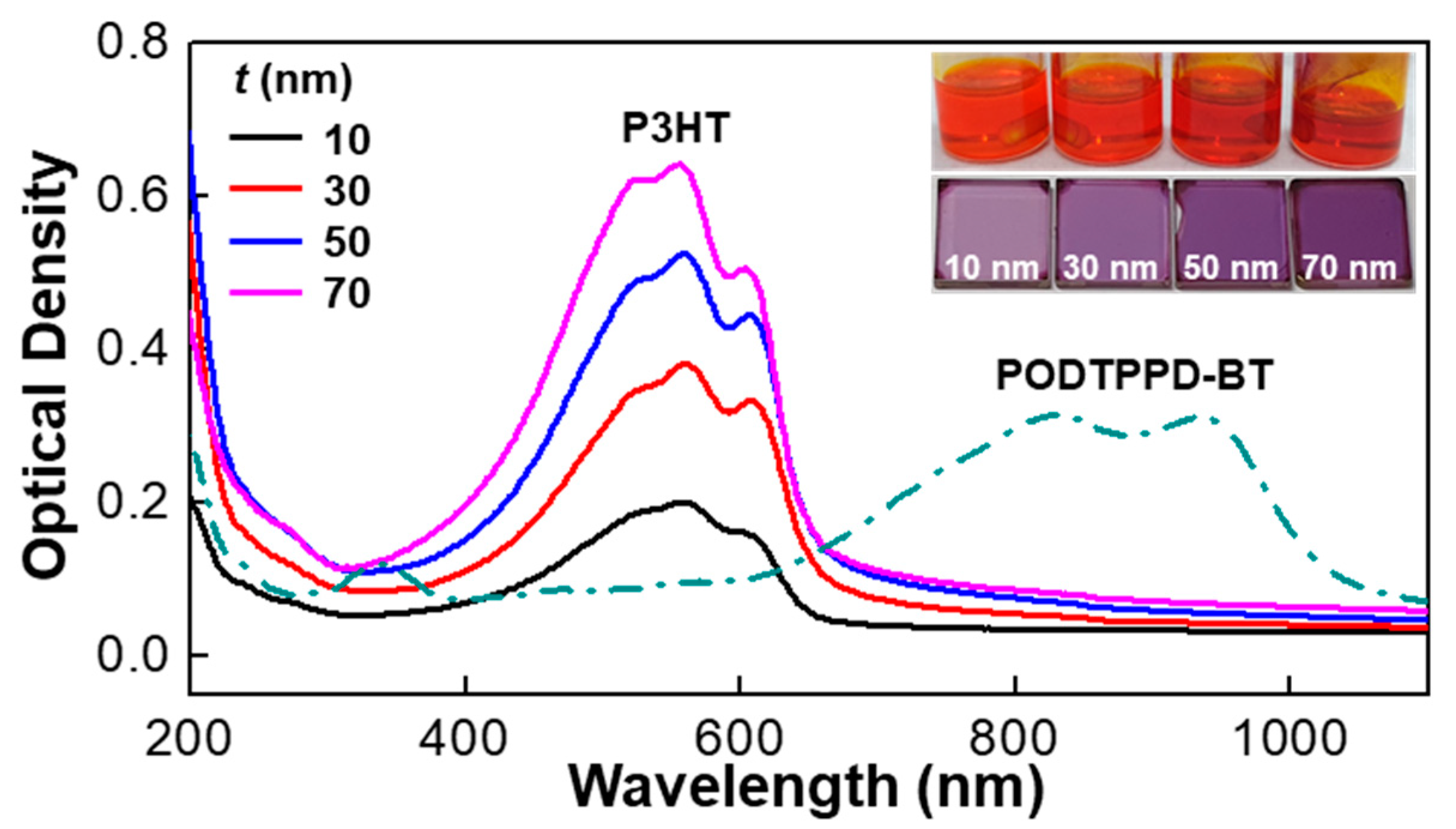
As displayed in Figure 2, the P3HT layers (films) exhibited a graded tint owing to their varied thicknesses even though the spectral shapes of the main optical absorption were similar in the presence of slightly changed intensity ratios among the three major peaks at 528, 556, and 604 nm. Here, it is noted that the NIR light intensity incident to the PODTPPD-BT layer is the same for all devices because the NIR light illuminates to the ITO-glass side of devices (see Figure 1a). In addition, the NIR light (780, 905, and 1000 nm) is assumed not to be absorbed by the P3HT layers so that the varied P3HT thickness cannot influence the net photocurrent by the NIR light. However, it is considered that the actual channel current of OFETs upon NIR illumination may be affected by the varied P3HT thickness, which is closely related with the overall field-effect generation of hole charges in the dark as well as upon illumination, when it comes to the role of P3HT channel thickness in Figure 1a (see the detailed discussion with transistor data below) [33,34,35].
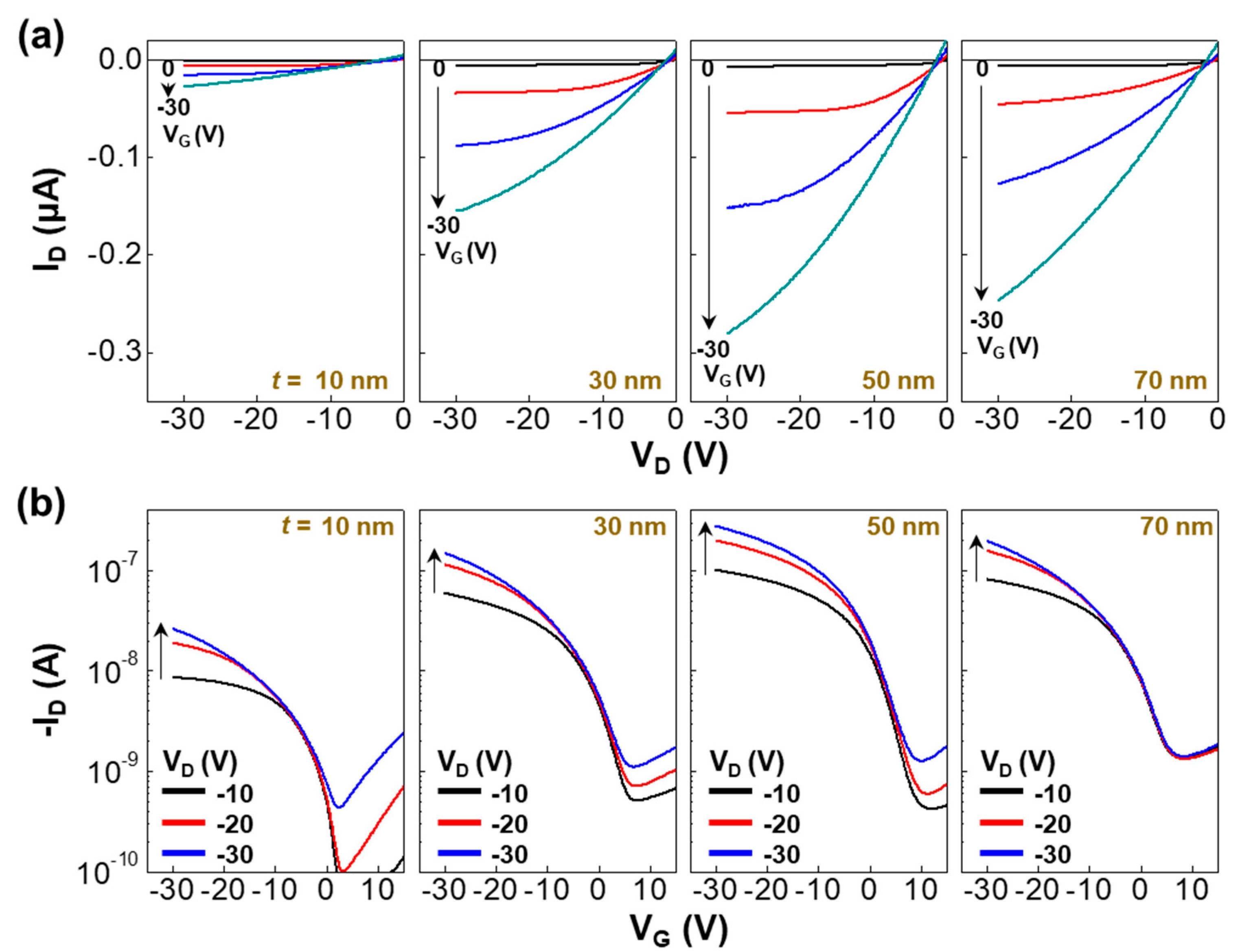
The basic performance of OFETs was first examined according to the P3HT thickness. As shown in Figure 3a, the output curves indicate that the present OFETs are typical p-channel transistors with a clear drain current (ID) increase (negatively) upon increasing the gate voltage (VG) and drain voltage (VD) negatively. As the P3HT thickness (t) increased, the drain current at a fixed gate and drain voltages was gradually increased up to t = 50 nm, but it was turned down by further increasing the P3HT thickness. As shown in Figure 3b, the transfer curves show that the drain current was negatively increased as the gate voltage increased negatively at a fixed drain voltage, which is in accordance with the output curves. In addition, a similar drain current trend with respect to the P3HT thickness was observed for both the output and transfer curves. This result supports that 50 nm may be an optimum P3HT thickness for maximizing the channel current in the present OFETs. The reason can be basically attributed to the thickness of the Ag source/drain electrodes (ca. 40~50 nm thick) because the extra part of the thick (t = 70 nm) P3HT layers might not act as an effective channel and the thin (t = 10 nm) P3HT layers could not deliver a sufficient volume for charge transport between the source and drain electrodes [36,37]. The relatively lower performance of the OFETs with the 70 nm-thick P3HT layers, compared to those with the 50 nm-thick P3HT layers, can be attributable to the different solution concentrations, leading to dissimilar Ag-P3HT interfaces and P3HT crystallizations. A close look into the transfer curves finds that the off-current level of devices became slightly higher at the thicker P3HT layers (t = 30~70 nm), compared to the devices with the 10 nm-thick P3HT layers, leading to the relatively low on/off ratios (59.6~274).
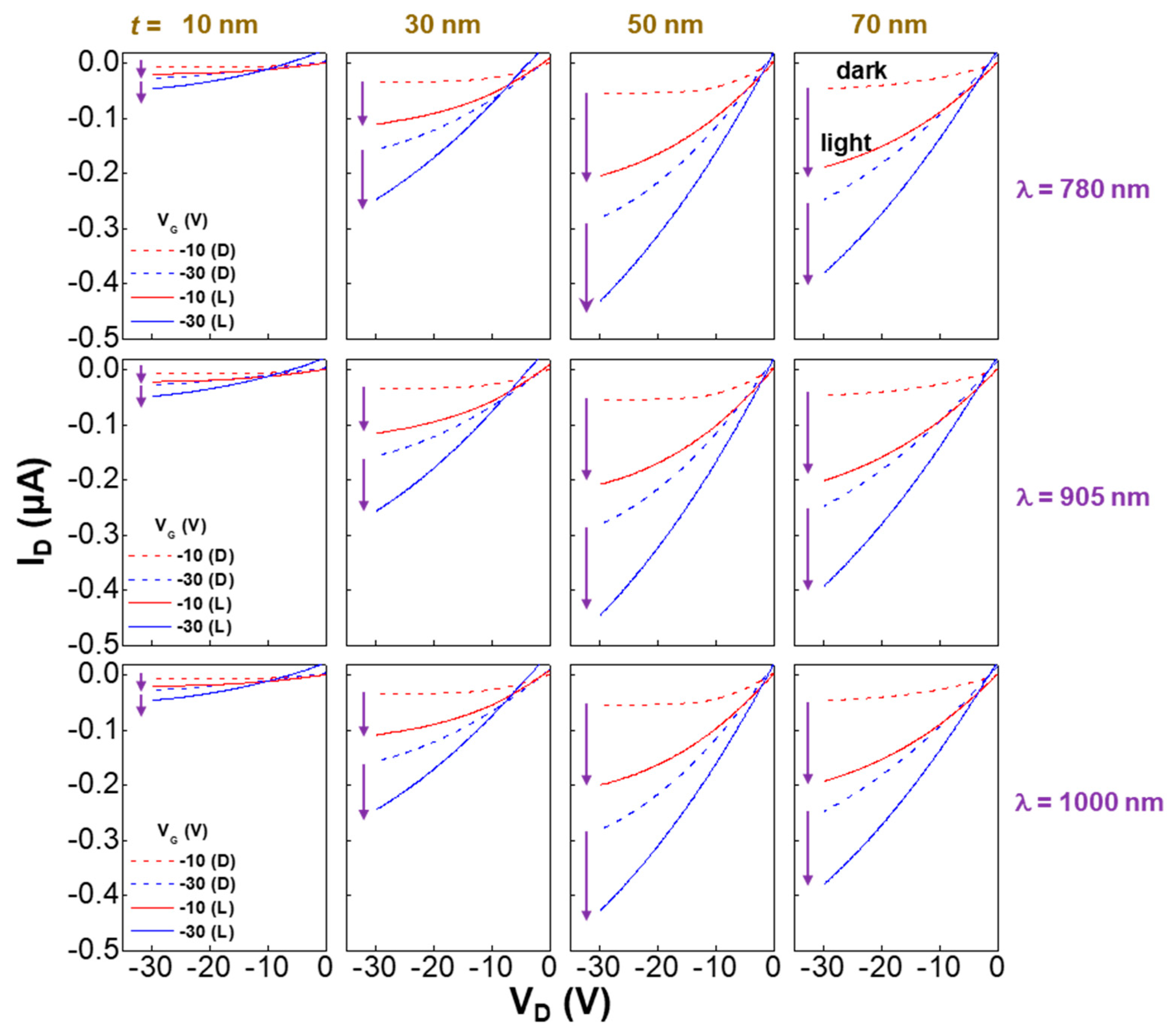
Next, the photoresponses of OFETs were measured under illumination with the three NIR light (780, 905, and 1000 nm). Note that the incident light intensity (PIN) of NIR light was adjusted to 0.27 mW cm−2 for the three wavelengths. As observed from the output curves in Figure 4, the drain current of all OFETs was increased upon illumination with the NIR light (λ = 780 nm) compared to the dark conditions. The maximum drain current under the NIR light illumination (λ = 780 nm) was measured at t = 50 nm, which simply indicates that overall, the photocurrent is dependent on the drain current in the dark. This trend was almost similar for the other two NIR lights (λ = 905 nm and 1000 nm). It is noted that the photocurrent level (under illumination) at VG = −10 V was lower than the drain current (in the dark) at VG = −30 V for all cases.
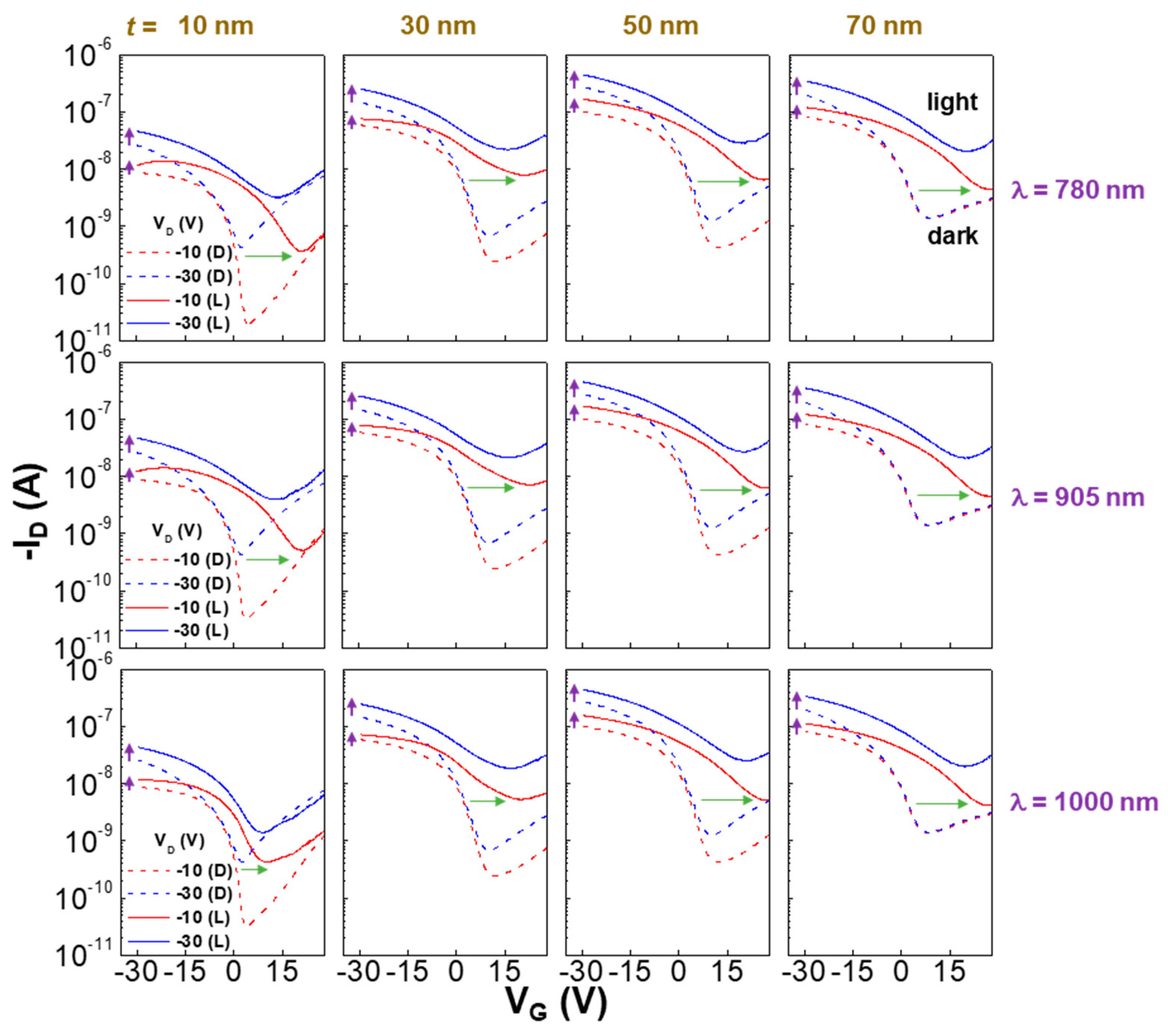
As shown in Figure 5, the transfer curves were noticeably changed upon illumination with the NIR light irrespective of the NIR wavelength. The drain current was increased under illumination with the NIR light for all cases, while the highest photocurrent was measured at t = 50 nm for all the three different wavelengths. Similar to the output curves, the photocurrent level at VD = −10 V and VG = −30 V was always lower than the drain current (in the dark) at VD = −30 V and VG = −30 V. This may reflect that the population of photogenerated charges in the PODTPPD-BT layer (GSL) at VD = −10 V is lower than that of field-effect charges in the P3HT channel layer at VD = −30 V. Particular attention is paid to the pronounced drain current increase in the off-current region by the NIR illumination, which can be attributed to the influence of photogenerated charges in the PODTPPD-BT layers [32]. As a consequence, the threshold voltage (VTH) of devices was shifted upon illumination (see green horizontal arrows in Figure 5). Note that the exact threshold voltage values can be obtained by the extrapolation (linear fitting) of ID0.5VG curves (the voltage at the zero point of ID0.5) [38,39].
The detailed shift of the threshold voltage between VTH, light and VTH, darkVTH) is plotted as a function of the P3HT thickness in Figure 6a. The highest threshold voltage shift was measured at t = 50 nm irrespective of the NIR wavelength, whereas the lowest threshold voltage shift was obtained at t = 10 nm. Interestingly, the NIR light with the shortest wavelength (λ = 780 nm) among the present three cases delivered the highest threshold voltage shift at t = 50 nm (note that a similar trend was measured at other thicknesses). This result cannot be explained only by the optical density in Figure 2 (OD = 0.28 at 780 nm, 0.30 at 905 nm, and 0.16 at 1000 nm) but can be attributable to various factors, including wavelength-dependent exciton generation efficiency (or charge separation efficiency) in the GSL and current combinations between source-gate and source-drain electrodes [32,40,41,42]. As shown in Figure 6b, the trend of the net photocurrent follows that of the dark drain current (see Figure 3) and the highest net photocurrent was achieved at t = 50 nm. In addition, the highest net photocurrent at a fixed P3HT thickness was obtained at 905 nm, which can be partly attributed to the highest optical density at this NIR wavelength but further correlated with wavelength-dependent quantum efficiency (theoretical maximum photoresponsivity discussed below) [43].
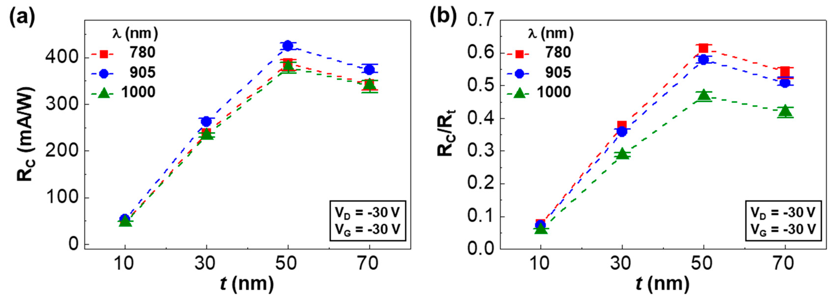
As shown in Figure 7a, the photoresponsivity (RC), which corresponds to the ratio of net photocurrent (IP = IlightIdark) to the incident light intensity (PIN = 0.27 mW cm−2), exhibited a gradual increase up to t = 50 nm and then it was slightly decreased at t = 70 nm. This trend was identical for the three NIR wavelengths. In particular, the maximum photoresponsivity at t = 50 nm is in good agreement with the threshold voltage shift (see Figure 6a). This result supports that the highest photoresponsivity can be achieved by maximizing the device performance (dark drain current) of organic phototransistors with a top channel layer. Here, it is noted that the NIR light at 905 nm resulted in the highest RC at a fixed P3HT thickness, which can be ascribed basically to the highest optical density at 905 nm but needs further consideration including the wavelength-dependent net photocurrent as discussed in Figure 6. Considering the different theoretical maximum photoresponsivity (Rt) with each wavelength (632 mA/W at 780 nm, 734 mA/W at 905 nm, and 810 mA/W at 1000 nm), which is only dependent on the NIR wavelength without any influence of materials, the ratio of RC to Rt was examined in order to clearly investigate the actual photoresponse efficiency [44]. As displayed in Figure 7b, the thickness-dependent trend was unchanged, but the ratio (RC/Rt) at a fixed thickness delivered the highest value at the shortest NIR wavelength (780 nm). The actual photoresponsivity of devices (t = 50 nm) reached ca. 61% of theoretical photoresponsivity at λ = 780 nm, and reached ca. 47% of theoretical photoresponsivity at λ = 1000 nm. The detailed parameters are summarized in Table 1.

4. Conclusions

The top P3HT channel layers were applied for the fabrication of GSL-OPTRs, which consist of Ag source/drain electrodes deposited on the PMMA/PODTPPD-BT layers. The P3HT thickness was varied from 10 to 70 nm in order to investigate its effect on the performance of GSL-OPTRs. The fabricated devices exhibited typical p-channel transistor behaviors in the presence of drain current saturation at a low gate voltage range (output characteristics). The highest drain current in the dark was measured at the P3HT thickness of 50 nm while the lowest one was obtained at 10 nm. The drain current was noticeably increased upon illumination with the NIR light irrespective of the wavelength and P3HT thickness, supporting the proper operation of GSL-OPTRs by the presence of PODTPPD-BT GSL even though the P3HT layers cannot absorb any NIR light. The transfer curves were pronouncedly shifted by the illumination of NIR light in the presence of a similarly increased drain current. The highest net photocurrent was achieved at t = 50 nm while the largest threshold voltage shift was also measured at the same P3HT thickness. As a result, the highest photoresponsivity (RC) among the present devices was achieved at t = 50 nm irrespective of the NIR wavelength. The present GSL-OPTRs with the 50 nm-thick P3HT top channel layers could reach ca. 61% photoresponsivity compared to theoretical maximum photoresponsivity at the NIR wavelength of 780 nm.

Author Contributions

Conceptualization, Y.K. and H.K.; methodology, Y.K. and H.K.; validation, J.P., T.K., H.K. and Y.K.; formal analysis, J.P., D.-I.S. and Y.K.; investigation, J.P., T.K. and Y.K.; resources, H.K. and Y.K.; data curation, J.P., C.L. and Y.K.; writing—original draft preparation, J.P.; writing—review and editing, Y.K. and H.K.; visualization, J.P., H.K., and Y.K.; supervision, Y.K.; project administration, Y.K.

Funding

The authors acknowledge research support by Kyungpook National University and additional funding from the National Research Foundation of Korea (2018R1D1A3B07046214 and Basic Science Research Program_2018R1A6A1A03024962).

Conflicts of Interest

The authors declare no conflict of interest.

References

  1. Harrison, M.T.; Kershaw, S.V.; Burt, M.G.; Rogach, A.L.; Kornowski, A.; Eychmuller, A.; Weller, H. Colloidal nanocrystals for telecommunications. Complete coverage of the low-loss fiber windows by mercury telluride quantum dot. Pure Appl. Chem. 2000, 72, 295–307. [Google Scholar] [CrossRef]
  2. Källhammer, J.-E. The road ahead for car night-vision. Nat. Photonics 2006, 5, 12–13. [Google Scholar] [CrossRef]
  3. Reutebuch, S.E.; Andersen, H.-E.; McGaughey, R.J. Light detection and ranging (LIDAR): An emerging tool for multiple resource inventory. J. For. 2005, 103, 286–292. [Google Scholar]
  4. Hong, G.; Antaris, A.L.; Dai, H. Near-infrared fluorophores for biomedical imaging. Nat. Biomed. Eng. 2017, 1, 0010. [Google Scholar] [CrossRef]
  5. Goswami, S.; Das, A.K.; Maity, A.K.; Manna, A.; Aich, K.; Maity, S.; Saha, P.; Mandal, T.K. Visual and near IR (NIR) fluorescence detection of Cr3+ in aqueous media via spirobenzopyran ring opening with application in logic gate and bio-imaging. Dalton Trans. 2014, 43, 231–239. [Google Scholar] [CrossRef] [PubMed] [Green Version]
  6. Werle, P.; Slemr, F.; Maurer, K.; Kormann, R.; Mücke, R.; Janker, B. Near- and mid-infrared laser-optical sensors for gas analysis. Opt. Lasers Eng. 2002, 37, 101–114. [Google Scholar] [CrossRef]
  7. Liang, F.-X.; Wang, J.-Z.; Li, Z.-P.; Luo, L.-B. Near-infrared-light photodetectors based on one-dimensional inorganic semiconductor nanostructures. Adv. Opt. Mater. 2017, 5, 1700081. [Google Scholar] [CrossRef] [Green Version]
  8. Zhuge, F.; Zheng, Z.; Luo, P.; Lv, L.; Huang, Y.; Li, H.; Zhai, T. Nanostructured materials and architectures for advanced infrared photodetection. Adv. Mater. Technol. 2017, 2, 1700005. [Google Scholar] [CrossRef]
  9. Luo, L.-B.; Chen, J.-J.; Wang, M.-Z.; Hu, H.; Wu, C.-Y.; Li, Q.; Wang, L.; Huang, J.-A.; Liang, F.-X. Near-infrared light photovoltaic detector based on GaAs nanocone array/monolayer graphene schottky junction. Adv. Funct. Mater. 2014, 24, 2794–2800. [Google Scholar] [CrossRef]
  10. Zhang, Y.; Li, Y.; Yan, X.-P. Photoactivated CdTe/CdSe quantum dots as a near infrared fluorescent probe for detecting biothiols in biological fluids. Anal. Chem. 2009, 81, 5001–5007. [Google Scholar] [CrossRef]
  11. Xu, R.-P.; Li, Y.-Q.; Tang, J.-X. Recent advances in flexible organic light-emitting diodes. J. Mater. Chem. C 2016, 4, 9116–9142. [Google Scholar] [CrossRef]
  12. Bansal, A.K.; Hou, S.; Kulyk, O.; Bowman, E.M.; Samuel, I.D.W. Wearable organic optoelectronic sensors for medicine. Adv. Mater. 2015, 27, 7638–7644. [Google Scholar] [CrossRef] [PubMed] [Green Version]
  13. Yokota, T.; Zalar, P.; Kaltenbrunner, M.; Jinno, H.; Matsuhisa, N.; Kitanosako, H.; Tachibana, Y.; Yukita, W.; Koizumi, M.; Someya, T. Ultraflexible organic photonic skin. Sci. Adv. 2016, 2, e1501856. [Google Scholar] [CrossRef] [PubMed] [Green Version]
  14. Song, M.; You, D.S.; Lim, K.; Park, S.; Jung, S.; Kim, C.S.; Kim, D.-H.; Kim, D.-G.; Kim, J.-K.; Park, J.; et al. Highly efficient and bendable organic solar cells with solution-processed silver nanowire electrodes. Adv. Funct. Mater. 2013, 23, 4177–4184. [Google Scholar] [CrossRef]
  15. Peumans, P.; Yakimov, A.; Forrest, S.R. Small molecular weight organic thin-film photodetectors and solar cells. J. Appl. Phys. 2003, 93, 3693–3723. [Google Scholar] [CrossRef]
  16. Renshaw, C.K.; Xu, X.; Forrest, S.R. A monolithically integrated organic photodetector and thin film transistor. Org. Electron. 2010, 11, 175–178. [Google Scholar] [CrossRef]
  17. Yan, F.; Liu, H.; Li, W.; Chu, B.; Su, Z.; Zhang, G.; Chen, Y.; Zhu, J.; Yang, D.; Wang, J. Double wavelength ultraviolet light sensitive organic photodetector. Appl. Phys. Lett. 2009, 95, 253308. [Google Scholar] [CrossRef]
  18. Lee, M.Y.; Hong, J.; Lee, E.K.; Yu, H.; Kim, H.; Lee, J.U.; Lee, W.; Oh, J.H. Highly flexible organic nanofiber phototransistors fabricated on a textile composite for wearable photosensors. Adv. Funct. Mater. 2016, 26, 1445–1453. [Google Scholar] [CrossRef]
  19. Pal, T.; Arif, M.; Khondaker, S.I. High performance organic phototransistor based on regioregular poly (3-hexylthiophene). Nanotechnology 2010, 21, 325201. [Google Scholar] [CrossRef]
  20. Noh, Y.-Y.; Kim, D.-Y. Organic phototransistor based on pentacene as an efficient red light sensor. Solid-State Electron. 2007, 51, 1052–1055. [Google Scholar] [CrossRef]
  21. Nam, S.; Seo, J.; Han, H.; Kim, H.; Bradley, D.D.C.; Kim, Y. Efficient deep red light-sensing all-polymer phototransistors with p-type/n-type conjugated polymer bulk heterojunction layers. ACS Appl. Mater. Interfaces 2017, 9, 14983–14989. [Google Scholar] [CrossRef] [PubMed]
  22. Hwang, H.; Kim, H.; Nam, S.; Bradley, D.D.C.; Ha, C.-S.; Kim, Y. Organic phototransistors with nanoscale phase-separated polymer/polymer bulk heterojunction layers. Nanoscale 2011, 3, 2275–2279. [Google Scholar] [CrossRef] [PubMed]
  23. Lee, C.; Lee, S.; Kim, H.; Kim, Y. UV-sensing semitransparent organic field-effect transistors with wide bandgap small molecular channel and polymeric gate-insulating layers. Adv. Electron. Mater. 2017, 3, 1700162. [Google Scholar] [CrossRef]
  24. Jung, J.H.; Yoon, M.J.; Lim, J.W.; Lee, Y.H.; Lee, K.E.; Kim, D.H.; Oh, J.H. High-performance UV–Vis–NIR phototransistors based on single-crystalline organic semiconductor–gold hybrid nanomaterials. Adv. Funct. Mater. 2017, 27, 1604528. [Google Scholar]
  25. Song, M.; Seo, J.; Kim, H.; Kim, Y. Ultrasensitive multi-functional flexible sensors based on organic field-effect transistors with polymer-dispersed liquid crystal sensing layers. Sci. Rep. 2017, 7, 2630. [Google Scholar] [CrossRef] [PubMed]
  26. Bhargava, K.; Bilgaiyan, A.; Singh, V. Two dimensional optoelectronic simulation based comparison of top and bottom contact organic phototransistors. J. Nanosci. Nanotechnol. 2015, 15, 9414–9422. [Google Scholar] [CrossRef] [PubMed]
  27. Lee, C.; Han, H.; Song, M.; Seo, J.; Kim, H.; Kim, Y. Organic phototransistors with chemically doped conjugated polymer interlayers for visible and near infrared light detection. IEEE J. Sel. Top. Quantum Electron. 2018, 24, 6000307. [Google Scholar] [CrossRef]
  28. Han, H.; Nam, S.; Seo, J.; Lee, C.; Kim, H.; Bradley, D.D.C.; Ha, C.-S.; Kim, Y. Broadband all-polymer phototransistors with nanostructured bulk heterojunction layers of NIR-sensing n-type and visible light-sensing p-type polymers. Sci. Rep. 2015, 5, 16457. [Google Scholar] [CrossRef] [Green Version]
  29. Wöbkenberg, P.H.; Labram, J.G.; Swiecicki, J.-M.; Parkhomenko, K.; Sredojevic, D.; Gisselbrecht, J.-P.; Leeuw, D.M.; Bradley, D.D.C.; Djukic, J.-P.; Anthopoulos, T.D. Ambipolar organic transistors and near-infrared phototransistors based on a solution-processable squarilium dye. J. Mater. Chem. 2010, 20, 3673–3680. [Google Scholar] [CrossRef]
  30. Sun, Z.; Li, J.; Yan, F. Highly sensitive organic near-infrared phototransistors based on poly(3-hexylthiophene) and PbS quantum dots. J. Mater. Chem. 2012, 22, 21673–21678. [Google Scholar] [CrossRef]
  31. Xu, H.; Li, J.; Leung, B.H.K.; Poon, C.C.Y.; Ong, B.S.; Zhang, Y.; Zhao, N. A high-sensitivity near-infrared phototransistor based on an organic bulk heterojunction. Nanoscale 2013, 5, 11850–11855. [Google Scholar] [CrossRef] [PubMed]
  32. Han, H.; Lee, C.; Kim, H.; Kim, Y. Flexible near-infrared plastic phototransistors with conjugated polymer gate-sensing layers. Adv. Funct. Mater. 2018, 28, 1800704. [Google Scholar] [CrossRef]
  33. Braga, D.; Horowitz, G. High-performance organic field-effect transistors. Adv. Mater. 2009, 21, 1473–1486. [Google Scholar] [CrossRef]
  34. Lee, J.; Kim, K.; Kim, J.H.; Im, S.; Jung, D.-Y. Optimum channel thickness in pentacene-based thin-film transistors. Appl. Phys. Lett. 2003, 82, 4169–4171. [Google Scholar] [CrossRef]
  35. Wang, Y.; Sun, X.W.; Goh, G.K.L.; Demir, H.V.; Yu, H.Y. Influence of channel layer thickness on the electrical performances of inkjet-printed In-Ga-Zn oxide thin-film transistors. IEEE Trans. Electron Devices 2010, 58, 480–485. [Google Scholar] [CrossRef]
  36. Pesavento, P.V.; Puntambekar, K.P.; Frisbie, C.D. Film and contact resistance in pentacene thin-film transistors: Dependence on film thickness, electrode geometry, and correlation with hole mobility. J. Appl. Phys. 2006, 99, 094504. [Google Scholar] [CrossRef]
  37. Dietz, G.W.; Antpöhler, W. Electrode influence on the charge transport through SrTiO3 thin films. J. Appl. Phys. 1995, 78, 6113–6121. [Google Scholar] [CrossRef]
  38. Tsuno, M.; Suga, M.; Tanaka, M.; Shibahara, K.; Miura-Mattausch, M.; Hirose, M. Physically-based threshold voltage determination for MOSFET’s of all gate lengths. IEEE Trans. Electron Devices 1999, 46, 1429–1434. [Google Scholar] [CrossRef]
  39. Wong, H.-S.; White, M.H.; Krutsick, T.J.; Booth, R.V. Modeling of transconductance degradation and extraction of threshold voltage in thin oxide MOSFET’s. Solid-State Electron. 1987, 30, 953–968. [Google Scholar] [CrossRef]
  40. Zhang, Y.; Yuan, Y.; Huang, J. Detecting 100 fW cm−2 light with trapped electron gated organic phototransistors. Adv. Mater. 2017, 29, 1603969. [Google Scholar] [CrossRef]
  41. Nam, S.; Kim, H.; Bradley, D.D.C.; Kim, Y. All-polymer phototransistors with bulk heterojunction sensing layers of thiophene-based electron-donating and thienopyrroledione-based electron-accepting polymers. Org. Electron. 2016, 39, 199–206. [Google Scholar] [CrossRef]
  42. Mok, S.M.; Yan, F.; Chan, H.L.W. Organic phototransistor based on poly(3-hexylthiophene)/TiO2 nanoparticle composite. Appl. Phys. Lett. 2008, 93, 023310. [Google Scholar]
  43. Lan, C.; Li, C.; Yin, Y.; Guo, H.; Wang, S. Synthesis of single-crystalline GeS nanoribbons for high sensitivity visible-light photodetectors. J. Mater. Chem. C 2015, 3, 8074–8079. [Google Scholar] [CrossRef]
  44. Casalino, M. Internal photoemission theory: Comments and theoretical limitations on the performance of near-infrared silicon Schottky photodetectors. IEEE. J. Quantum Electron. 2016, 52, 4000110. [Google Scholar] [CrossRef]
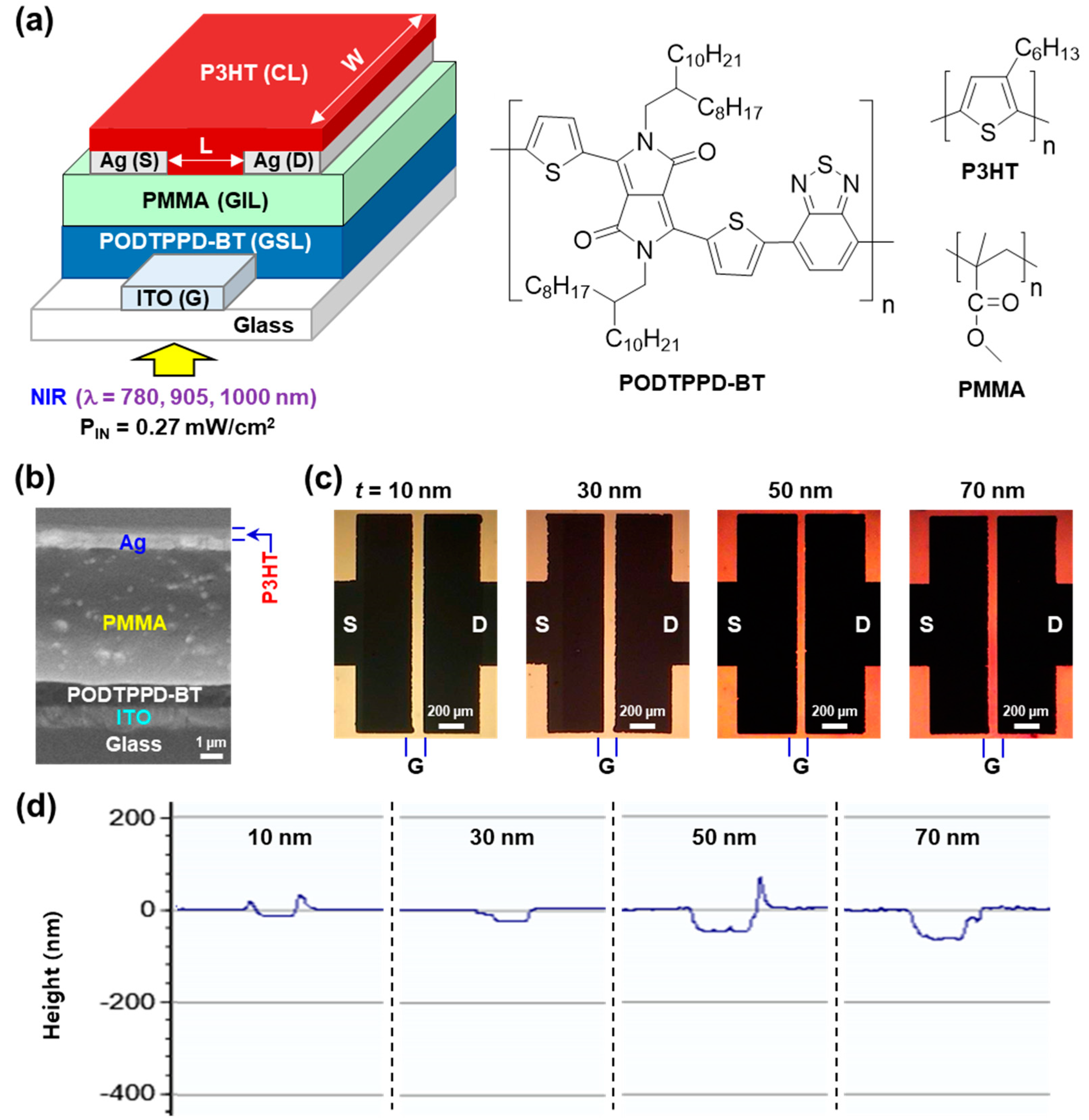
Figure 1. (a) Device structure for the GSL-OPTRs with P3HT top channel layers and PODTPPD-BT gate-sensing layers: L and W denote the channel length and width, respectively. The corresponding chemical structures of PODTPPD-BT, P3HT, and PMMA are given on the right part. (b) SEM image for the cross-section of device (note that some big spots were made during breaking the devices at room temperature). (c) Optical microscope images from the top part of devices according to the P3HT thickness. (d) Thickness profile data for the P3HT channel layers that were scribed for measurements (center parts) after film coating processes.
Electronics 08 01493 g001
Figure 2. Optical absorption spectra of P3HT films (according to their thickness) and PODTPPD-BT film (100 nm thick) coated on quartz substrates (inset: photographs for the P3HT solutions (toluene) and films).
Electronics 08 01493 g002
Figure 3. (a) Output and (b) transfer characteristics of OFETs in the dark according to the P3HT thickness. Note that VG and VD were negatively increased by −10 V in the output and transfer curves, respectively.
Electronics 08 01493 g003
Figure 4. Change of output curves upon NIR illumination for the GSL-OPTRs according to the P3HT thickness (t = 10, 30, 50, and 70 nm). The dashed lines denote drain current in the dark, while the solid lines represent overall photocurrent under illumination with the NIR light (λ = 780, 905, and 1000 nm) at VG = −10 V and −30 V (see arrows for the increased drain current). The incident light intensity (PIN) was controlled to 0.27 mW cm−2 for all wavelengths.
Electronics 08 01493 g004
Figure 5. Change of transfer curves upon NIR illumination for the GSL-OPTRs according to the P3HT thickness (t = 10, 30, 50, and 70 nm). The dashed lines denote drain current in the dark, while the solid lines represent overall photocurrent under illumination with the NIR light (λ = 780, 905, and 1000 nm) at VG = −10 V and −30 V (see arrows for the increased drain current). The incident light intensity (PIN) was controlled to 0.27 mW cm2 for all wavelengths. The green horizontal arrows indicate the shift of transfer curves upon light illumination at VG = −10 V.
Electronics 08 01493 g005
Figure 6. (a) Threshold voltage shift (ΔVTH = VTH, lightVTH, dark) as a function of P3HT thickness (t) according to the wavelength (λ) of incident NIR light. (b) Net photocurrent (ΔID = ID, lightID, dark) as a function of P3HT thickness (t) according to the wavelength (λ) of incident NIR light (at VD = VG = −30 V).
Electronics 08 01493 g006
Figure 7. (a) Photoresponsivity (RC) and (b) ratio of RC to Rt as a function of P3HT thickness (t) according to the wavelength (λ) of incident NIR light (at VD = VG = −30 V). Rt stands for theoretical maximum responsivity at each wavelength.
Electronics 08 01493 g007
Table 1. Summary of photoresponsivity (RC) and threshold voltage shift (ΔVTH) according to the P3HT thickness (t) and NIR wavelength (λ). RC values were obtained from the transfer curves at VD = VG = −30 V.
λ (nm)Parameterst (nm)
10305070
780RC (mA/W)47.64237.91388.43342.90
ΔVTH (V)20.8922.2625.6923.05
905RC (mA/W)53.05262.68424.93372.52
ΔVTH (V)17.1320.9922.3421.56
1000RC (mA/W)47.13232.91379.33339.94
ΔVTH (V)16.7718.7321.7620.90