Abstract
CMOS analog baseband circuits including a low-pass filter (LPF) and a programmable gain amplifier (PGA) are designed and implemented for the fifth-generation (5G) mobile communication. The super source follower topology is adopted to achieve a wideband LPF with good linearity, while the constant current density gain control technique is used to implement gain cells of the PGA. The circuits are integrated as an analog baseband for a 5G transmitter (TX) and fabricated using TSMC 90-nm CMOS technology. The analog baseband exhibits the bandwidth from 1.03 to 1.05 GHz when the voltage gain is varied from −18.9 dB to 3.8 dB in 1-dB steps. The gain step errors are within −0.7 dB to +0.9 dB. In the highest gain mode, the analog baseband achieves the IP1dB of −10 dBv and the IIP3 of −0.2 dBv. Over the band of interest, the NF of the analog baseband is 24.4–40.0 dB.
1. Introduction
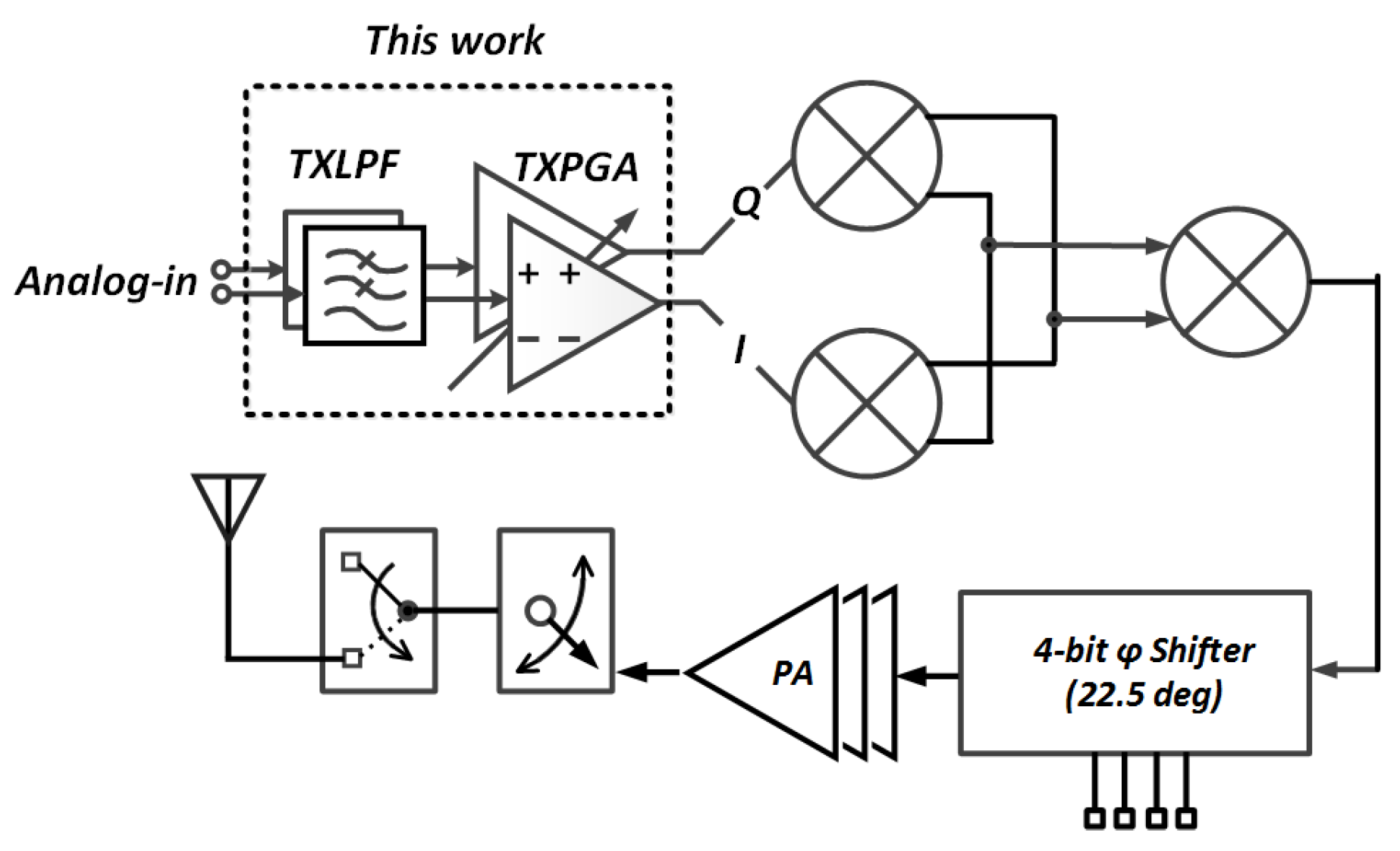
The vision, spectrum, and technology views of the fifth-generation (5G) mobile communication have been fully rolled out. In 2020, the definition of 5G technology will also be finalized. According to the 5G standard, IMT 2020, the total download capacity for a single 5G mobile cell must be at least 20 Gbps [1]. A channel bandwidth of at least 1 GHz would be demanded to accommodate the wideband signals. Therefore, it is necessary for analog baseband circuits in RF transceivers to achieve the bandwidth above 1 GHz. Figure 1 shows the block diagram of an RF transmitter for 5G mobile communication. The baseband signals from the digital-to-analog converter would be delivered to the analog baseband including the low-pass filter (LPF) and the programmable gain amplifier (PGA). Then the LPF provides out-of-band rejection to solve the anti-aliasing issue, while the PGA maintains the adequate signal level for the up-conversion mixer. The object of this work is to design these analog baseband circuits.
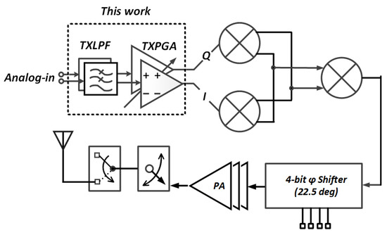
Figure 1.
Transmitter block diagram.
For LPFs, large out-of-band rejection can be achieved by increasing the filter order or introducing transmission zeroes. Increasing the filter order usually leads to higher power consumption. Moreover, it may raise stability and noise issues. Therefore, filters equipped with transmission zeroes are better choices for wireless applications that require high out-of-band rejection. With transmission zeroes allocated in the stopband, Elliptic filters can achieve higher attenuation, as compared to Chebyshev or Butterworth filters, so they have been commonly used in modern wireless communication systems supporting multi-carrier modulation [2,3,4].
In general, dB-linear PGAs can be categorized into close-loop and open-loop amplifiers. For a close-loop amplifier, good linearity can be achieved due to the feedback architecture, while the dB-linear gain can be easily obtained since the gain is usually determined by the ratio between resistors [5]. However, it requires numerous resistors and switches to achieve the small gain step error, which results in large chip area. The transistors, as switches of the resistor array in the feedback network, usually operate in the triode region and introduce a significant source of nonlinearity. The open-loop amplifiers may be more suitable for 5G applications considering the low power and wideband characteristics, where the wide bandwidth can be easily achieved without stability issues. The required gain range can be obtained by connecting multiple gain stages in cascade and using several linear terms for each gain stage [6,7,8,9].
In this work, a transmitter analog baseband for 5G mobile communication is designed and implemented. The Elliptic filter is adopted to realize the LPF, while the open-loop amplifier is adopted to realize the dB-liner PGA. The rest of the paper is organized as follows. In Section 2, the design of the LPF and PGA would be presented. In Section 3, the measurement results of the LPF and the transmitter analog baseband would be reported. Finally, the conclusion would be given in Section 4.
2. Circuits Design
2.1. Low-Pass-Filter (LPF)
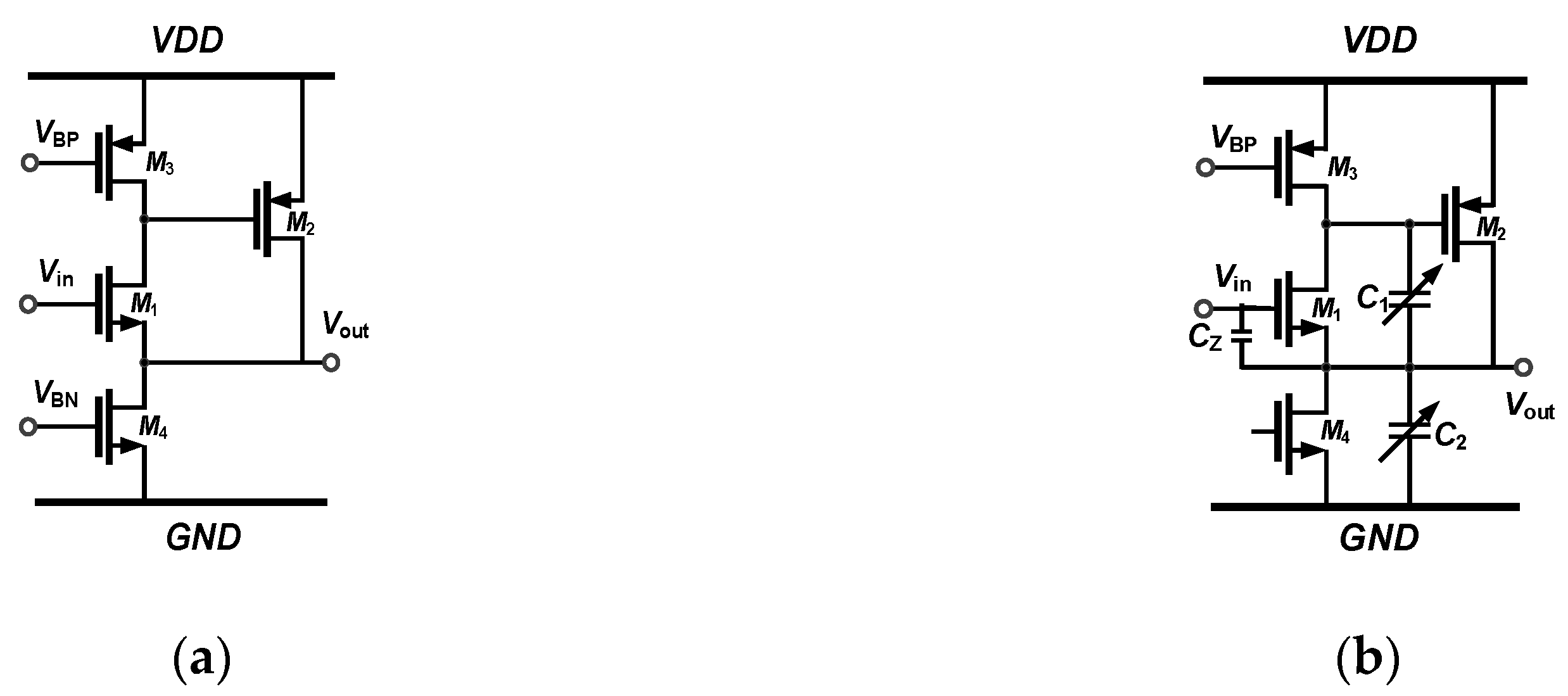
Because of the characteristics of high input resistance and low output resistance, source followers are often used as buffers. In fact, they can be simply modified into continuous-time filters by synthesizing complex poles with the feedback and capacitors [3]. A super source follower is an improved version of the source follower. By adding an additional MOSFET to form a feedback loop, the output impedance can be reduced by a factor of the loop gain [4]. In this work, a super source follower based low-pass-filter is implemented. Figure 2a shows the schematic of a super-source-follower (SSF). The super source follower contains an additional local feedback formed by the transistor M2. Transistors M3 and M4 are current sources. The output resistance of the SSF can be analyzed as follows. The input voltage is kept constant and let us assume that the output now experiences a voltage drop. The voltage drop not only raises the drain current of M1 but also lowers the gate voltage of M2. Hence, the drain current of M2 would be increased. The output resistance is therefore reduced because of this incremental current flow through the output node. The output resistance of an SSF can be expressed as:
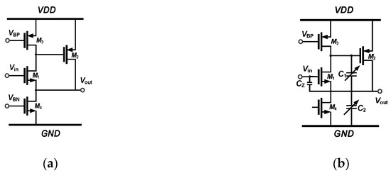
Figure 2.
Schematics of (a) NMOS-input super-source-follower (SSF) and (b) SSF-based biquadratic low-pass filter.
Notably, the output resistance of SSF is lower by a factor of gm2ro3, as compared with that of a conventional source follower. The dc voltage gain A0, is given in Equation (2), where the output resistance ro of each transistor is considered:
The resistor ro24 represents the equivalent resistance of resistors ro2 and ro4 in parallel. With the reduced output resistance and improved gain, the SSF shows better driving capability, as compared to the traditional source follower.
The SSF is modified into a biquadratic low-pass filter, as shown in Figure 2b, where capacitors C1 and C2 are employed to synthesis poles. In parallel with the main signal path, the gate-source capacitance of M1 (Cgs1) is naturally associated with a high frequency zero. Since the LPF requires a transmission zero at 2.2 GHz, a capacitor CZ is included to move the transmission zero to the desired frequency. The transfer function of the SSF-based biquadratic filter is expressed in (3):
From the formula (3), the complex pole ω0, the quality factor Q and the transmission zero ωz can be obtained, as expressed in (4), (5), and (6) respectively:
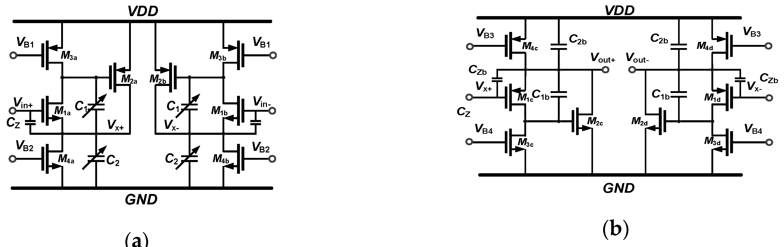
In this work, a fourth-order Elliptic LPF is designed to provide anti-aliasing function for 5G mobile communication. The fourth-order LPF is formed from two SSF biquadratic low-pass filters in cascade, as shown in Figure 3, where the two filters use different types of input transistors so that the level shifting effect is compensated to obtain identical input and output common mode voltages [4]. At the initial stage of design, the software “Filter Solutions” is used to determine the key parameters for the fourth-order Elliptic LPF. According to the calculation results of “Filter Solutions”, the cut-off frequency, transmission zero, and quality factor of the first biquadratic low-pass filter are set to 707 MHz, 2.2 GHz, and 0.73, respectively, while the cut-off frequency, transmission, and quality factor of the second biquadratic low-pass filter are set to 1.13 GHz, 5.27 GHz, and 3.45, respectively. Since small capacitors are used to synthesize high-frequency poles and zeroes, the LPF is very susceptible to parasitic capacitances. In order to achieve the desired frequency response, the capacitors C1, C2, and CZ in the biquadratic low-pass filter are chosen by considering all the inevitable parasitic capacitances in the circuit. Moreover, the capacitors C1 and C2 are realized with 2-bit programmable capacitors in the first biquadratic low-pass filter so that the corner frequency and transmission zero of the LPF can be tuned to cope with process-voltage-temperature variations.
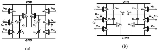
Figure 3.
Schematics of the (a) first biquadratic low-pass filter and (b) second biquadratic low-pass filter of the low-pass filter (LPF).
2.2. Programmable Gain Amplifier (PGA)
Unwanted spurs appearing in the output spectrum of an up-conversion mixer can cause serious spectrum regrowth. Since their levels are closely related to the input level of the mixer, it is necessary for the PGA to pass the mixer with a specified signal level so that these spurs can be down by 40–50 dBc. According to the simulation results of the up-conversion mixer, the desired input level of the mixer is 200 mVpp. Therefore, the PGA is designed to maintain the output level of 200 mVpp for an input dynamic range of 20 dB. With the programmable voltage gain from −16 dB to 4 dB, the PGA can handle the input level from 1.26 Vpp to 126 mVpp.
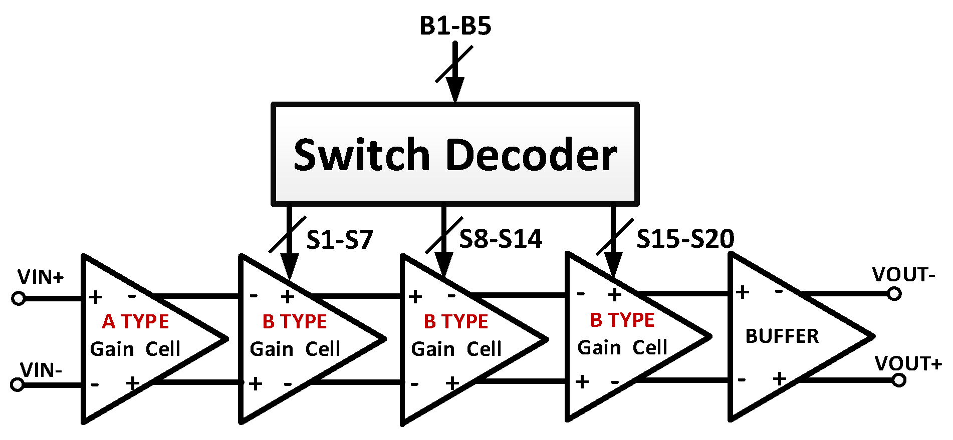
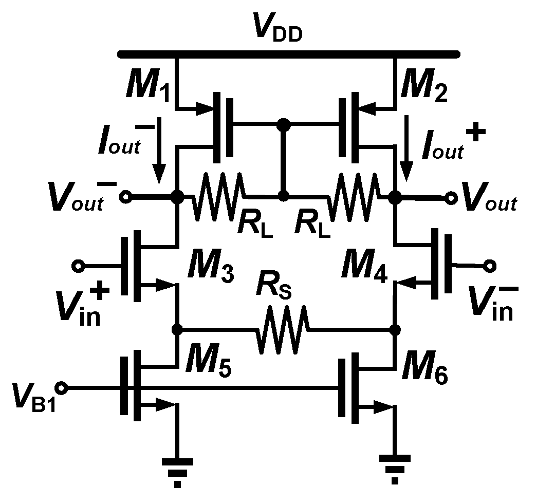
An open-loop-configured PGA is designed and implemented to achieve the required gain range. The block diagram of the programmable gain amplifier is shown in Figure 4. Considering the tradeoff between the power consumption and bandwidth, four gain cells are connected in cascade to achieve the desired gain range. The 5-bit binary control word B1–B5 is translated into the 20-bit thermometer code S1–S20 by a switch decoder, as shown in Figure 4. The first gain cell (A-type gain cell) of the PGA is a common-source amplifier with resistive source degeneration (Figure 5). This gain cell provides the gain of −16 dB so that large baseband signals can be attenuated in the first stage. In this way, the linearity requirement of the rest gain cells can be relaxed.
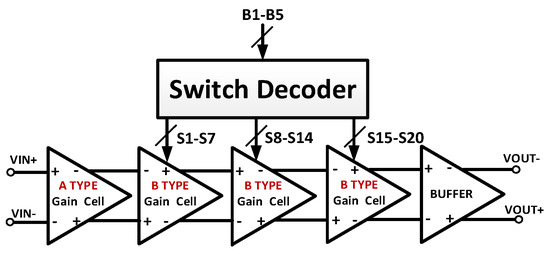
Figure 4.
Programmable gain amplifier (PGA) block diagram.

Figure 5.
Schematic of A-type gain cell.
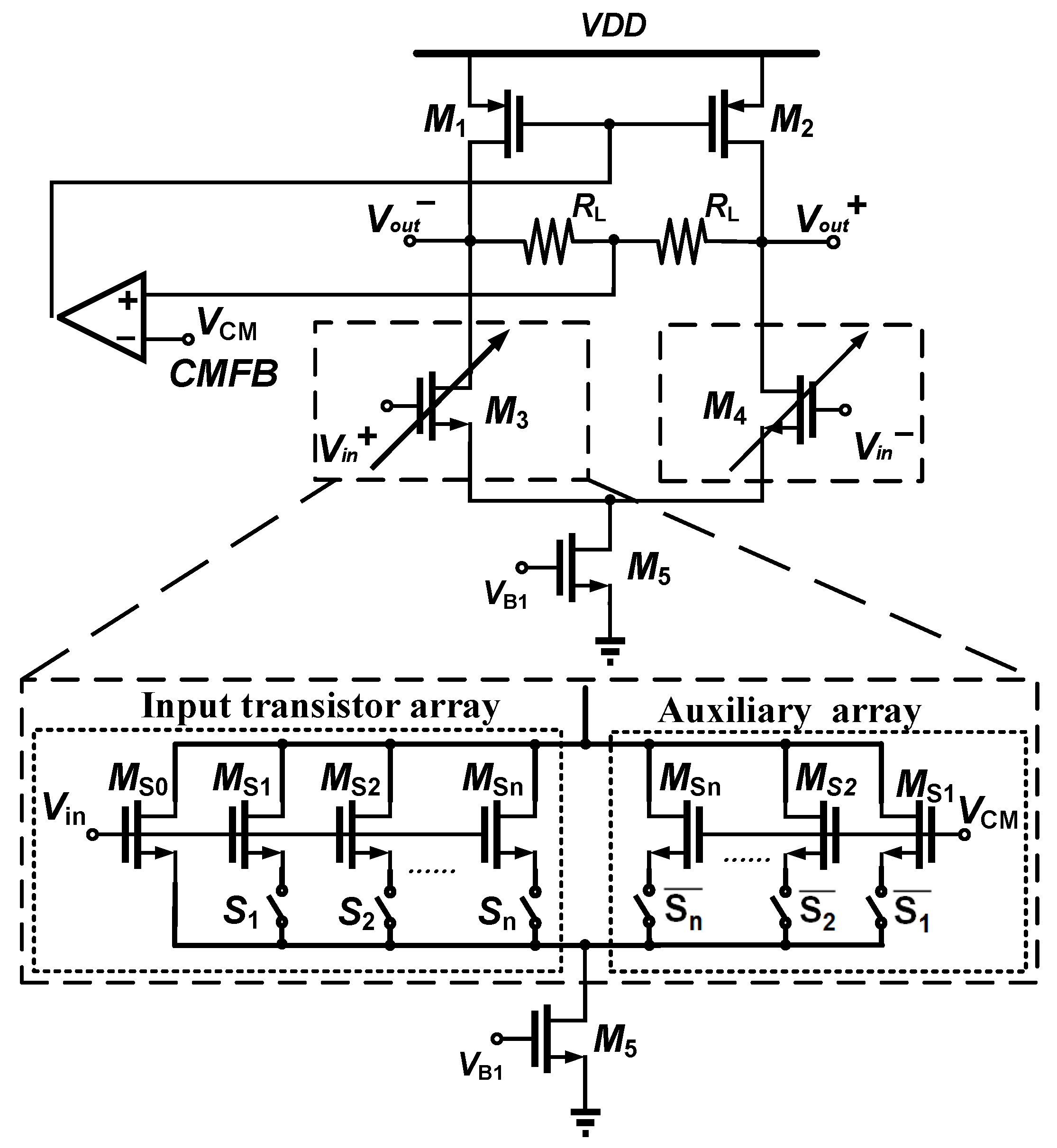
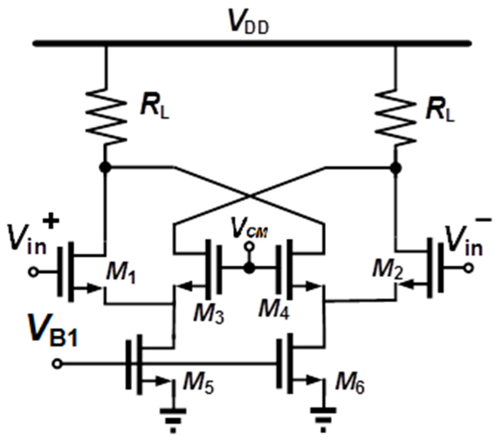
The rest gain cells (B-type gain cell) are common-source amplifiers using the constant current density function (Figure 6) [9]. Each B-type gain cell contains two transistor arrays (an input transistor array and an auxiliary array), connected in parallel, where each transistor in the arrays is connected with a switch in series. The switches controlled by the digital word S1–Sn would be used to turn on or off the corresponding transistors MS1–MSn in the input transistor array while the switches controlled by the digital word would be used to turn on or off the corresponding transistors MS1–MSn in the auxiliary array. In particular, the auxiliary array is applied with same input DC level (VCM) and contains transistors identical to those in the input transistor array so that the output dc level can remain constant for each gain mode [9].

Figure 6.
Schematic of B-type gain cell [9].
If KS0–KSn represent the W/L ratios of the corresponding transistors MS0–MSn, then the effective W/L ratio Kn of the input transistor array can be expressed as:
The effective transconductance gmn can be expressed as:
The gain equals the product of the effective transconductance gmn and the load resistor RL, and can be expressed as follows:
The voltage gain of each B-type gain cell can be varied from 0 to 7 dB in 1-dB steps. When all the gain cells are connected in cascade (as shown in Figure 4), the gain range of 20 dB can be provided. During the simulation, the PGA delivers the voltage gain of 3.92 dB and −16.1 dB for the 5-bit binary programming word of 10,100 and 00,000, respectively.
A buffer (Figure 7) is used to drive the 50-Ω load of the network analyzer during the measurement. Moreover, it can also maintain the required bandwidth and linearity by minimizing the loading effect of the up-conversion mixer in the future. Based on the fT-doubler architecture, the buffer delivers a high output current to extend the unit-gain frequency. During the simulation, the loading effect is considered by connecting an up-conversion mixer to the output of the buffer. According to the simulation, the buffer achieves the total harmonic distortion (THD) of −47 dB for the input level of 200 mVpp and the 3-dB bandwidth of 1.7 GHz.
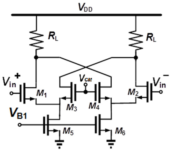
Figure 7.
Schematic of the buffer.
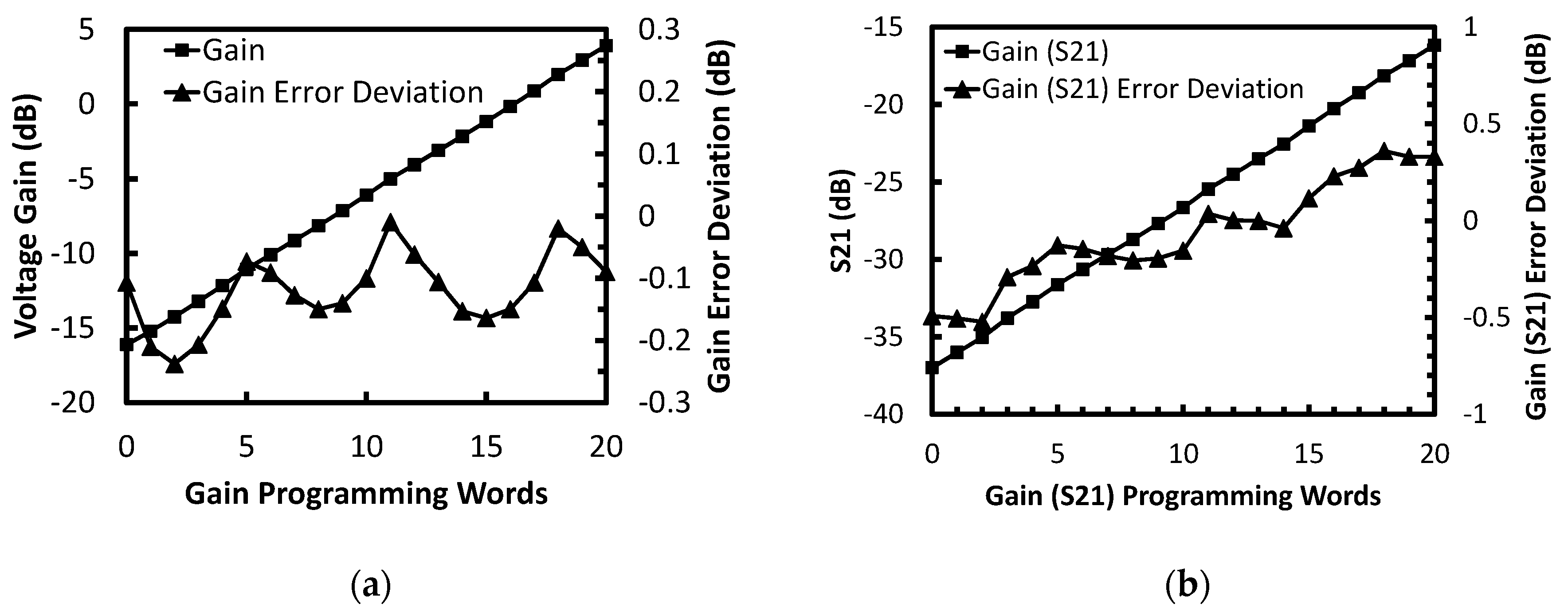
The frequency response of the PGA is observed in different gain modes during the simulation. The PGA exhibits the 3-dB bandwidth above 1.2 GHz in all the gain modes. The power gain S21 is more available for the measurement with frequency range up to 1–2 GHz, while the voltage gain is specified as the requirement for analog baseband circuits, so the simulation is performed to observe both the voltage gain and power gain S21. The simulation results of the voltage gain and gain error deviation in all the gain modes are shown in Figure 8a. The gain step error is within ± 0.11 dB and the maximum gain error deviation is less than 0.23 dB. The simulation results of the S21 and gain error deviations in all the gain modes are shown in Figure 8b. The gain step error is within ± 0.23 dB and the maximum gain error deviation is less than 0.52 dB. According to the simulation results, the circuit delivers the voltage gain of 3.92 dB in the highest gain mode and the corresponding S21 is −16.17 dB. In the lowest gain mode, the circuit delivers the voltage gain of −16.1 dB and the corresponding S21 is −36.99 dB.

Figure 8.
(a) Simulated voltage gain and gain error deviation of the PGA. (b) Simulated S21 and gain error deviation of the PGA.
The Monte Carlo simulation results of the 5G transmitter (TX) analog baseband are shown in Figure 9. Both the process variation and device mismatch are considered in the Monte Carlo simulation. The number of runs is set to 100 for the Monte Carlo simulation. The simulation results of the AC response in the highest gain mode are shown in Figure 9a, where the gain variation is from −3.05 dB to 8.46 dB, and the corner frequency variation is from 1.12 MHz to 1.42 MHz. The simulation results of the S21 in the highest gain mode are shown in Figure 9b, where the gain variation is from −20.5 dB to −12.81 dB, and the corner frequency variation is from 1.211 MHz to 1.447 MHz.
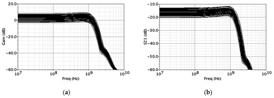
Figure 9.
(a) Simulated AC response of the PGA by Monte Carlo Simulation. (b) Simulated S21 of the PGA by Monte Carlo Simulation.
3. Measurement Results
The TX analog baseband consisting of the LPF and PGA is fabricated in TSMC 90-nm CMOS process. The chip photo is shown in Figure 10 and the circuit occupies an active area of 0.24 mm2. According to the simulation, the circuit consumes 43 mW when it operates under the 1.2 V supply. However, the circuit consumes the power of 93 mW from the 1.2-V supply during the measurement. Such discrepancy may result from the gate leakage current.
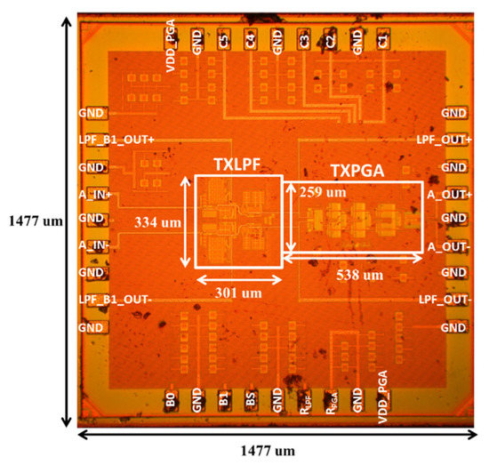
Figure 10.
Chip photo of the 5G transmitter (TX) analog baseband.
3.1. LPF Measurement Result
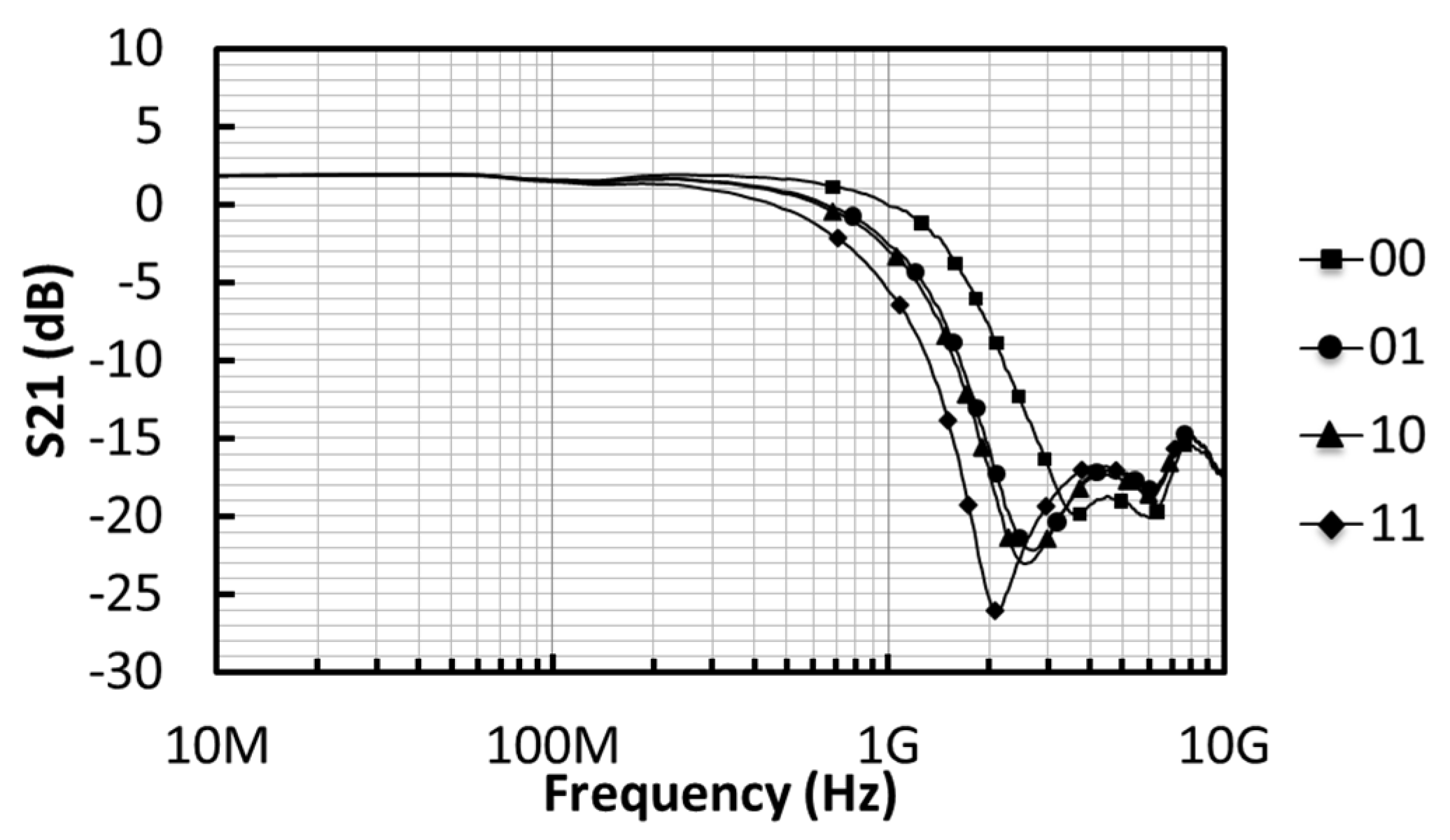
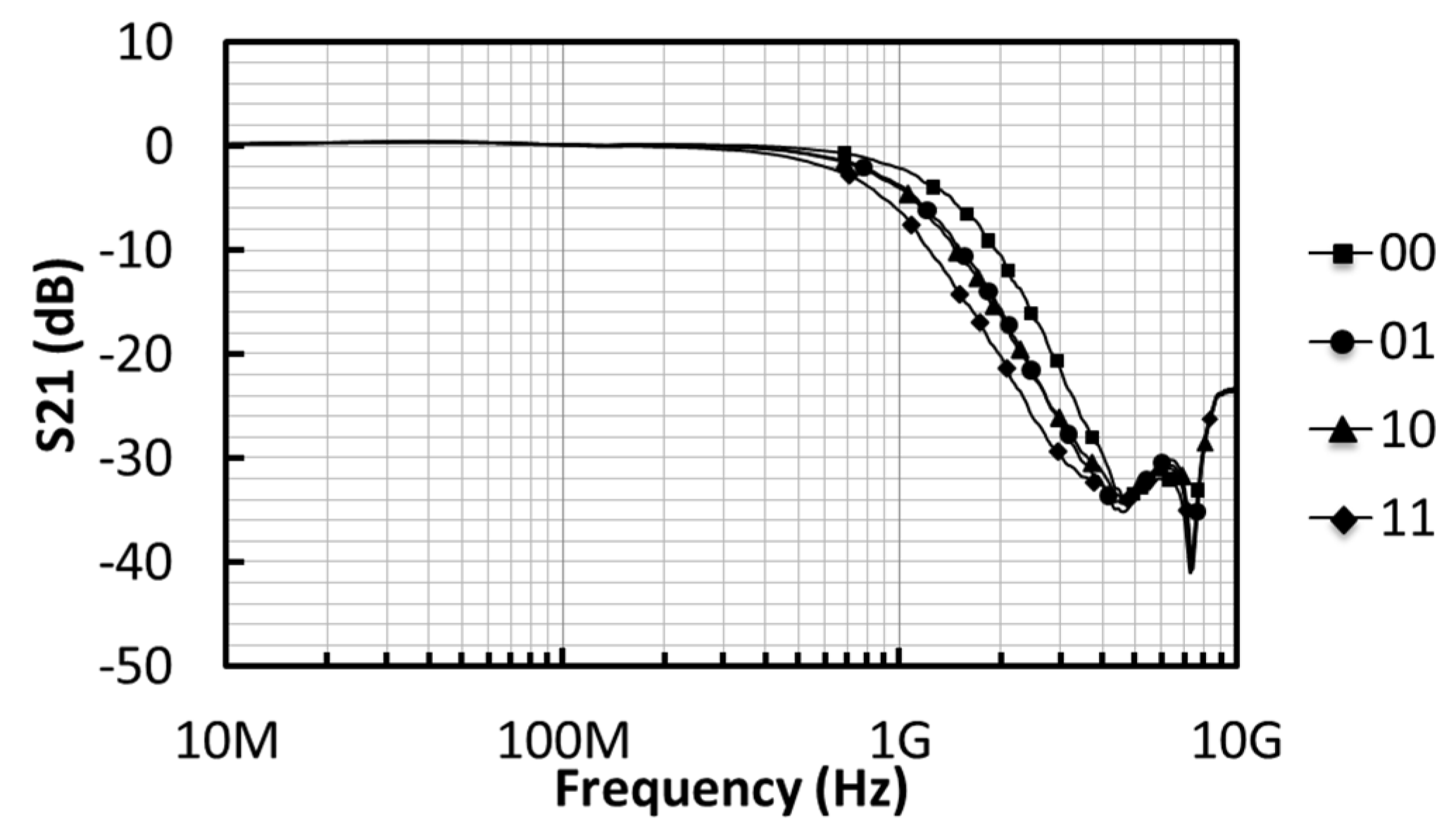
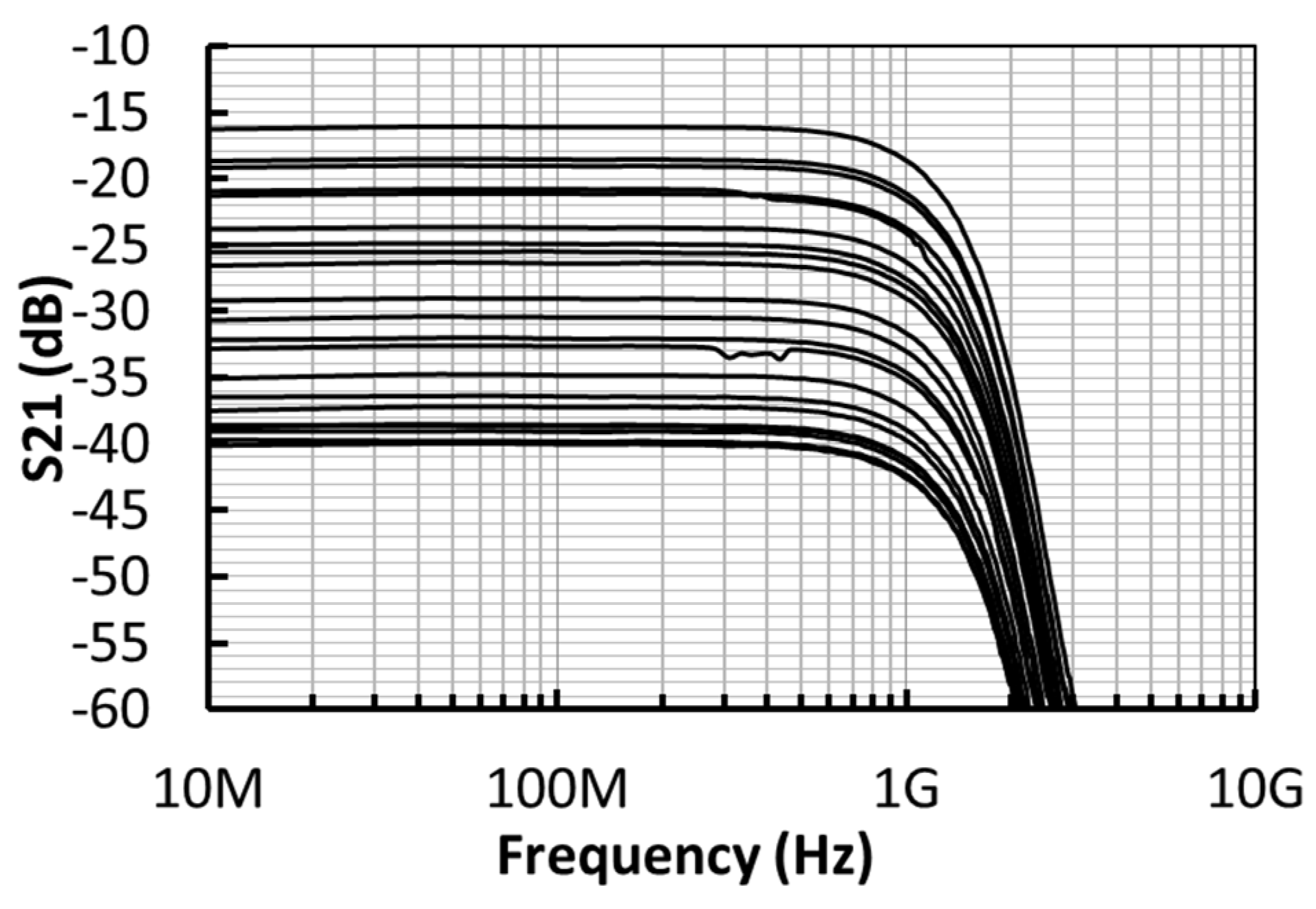
The measured S21 of the first biquadratic filter is shown in Figure 11. With the 2-bit programmable capacitor, the cut-off frequency of the first biquadratic filter can be varied from 0.58 GHz to 1.2 GHz, with the transmission zero correspondingly varied from 2.03 GHz to 3.33 GHz. Figure 12 shows the measured S21 of the fourth-order Elliptic LPF. The cut-off frequency ω0 and transmission zeroes ωZ1 and ωZ2 are listed in Table 1. The cut-off frequencies can be varied from 0.76 GHz to 1.23 GHz, while the first transmission zero can be varied from 2.03 to 3.33 GHz. The second transmission zero would remain at 4.6 GHz in all the operation modes.
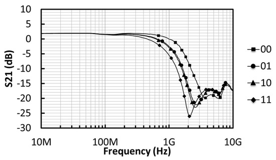
Figure 11.
Measured S21 of the first biquadratic filter.

Figure 12.
Measured S21 of the fourth-order Elliptic LPF.

Table 1.
Fourth-order Elliptic LPF Cut-off and Zero Frequencies.
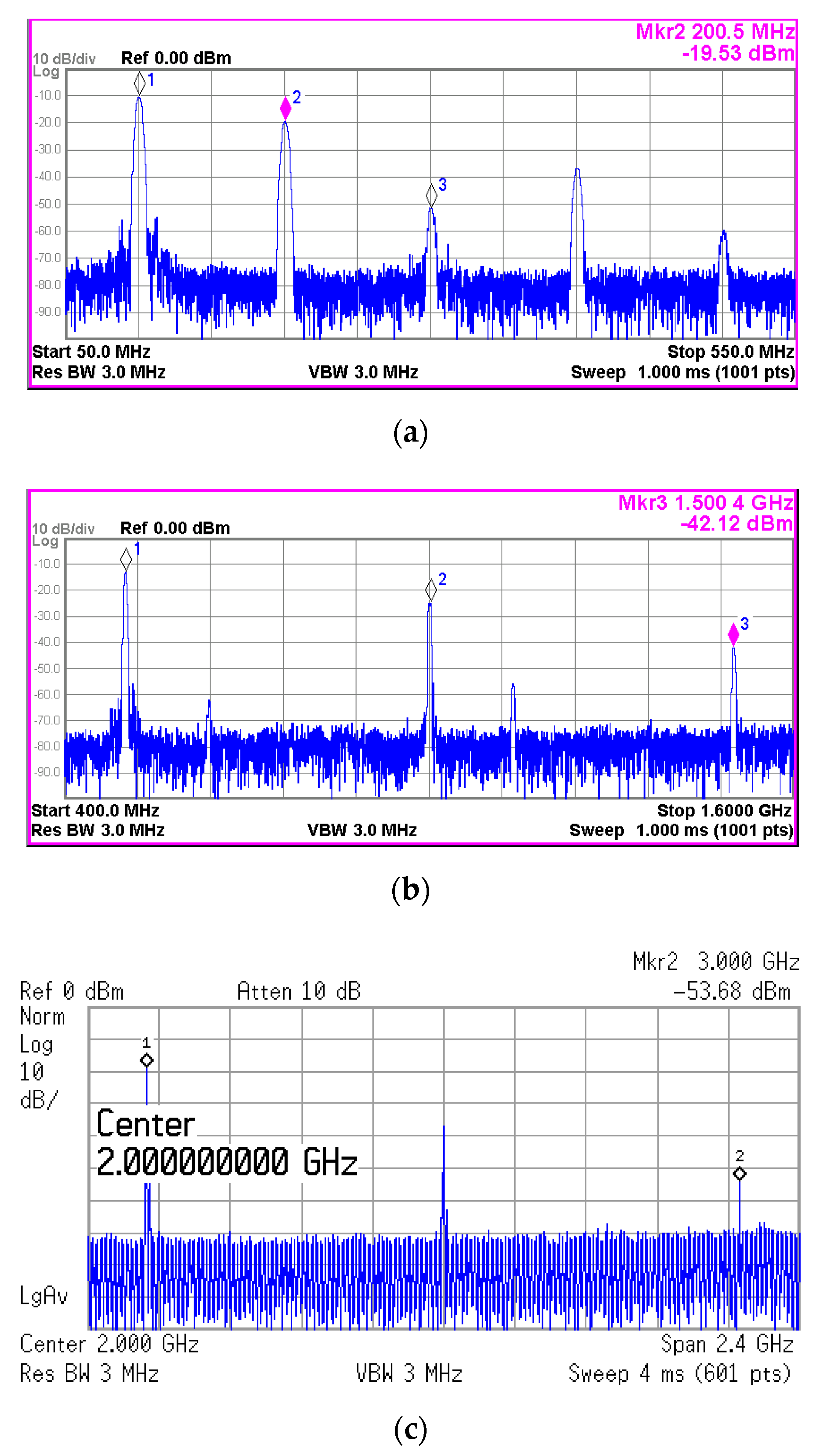
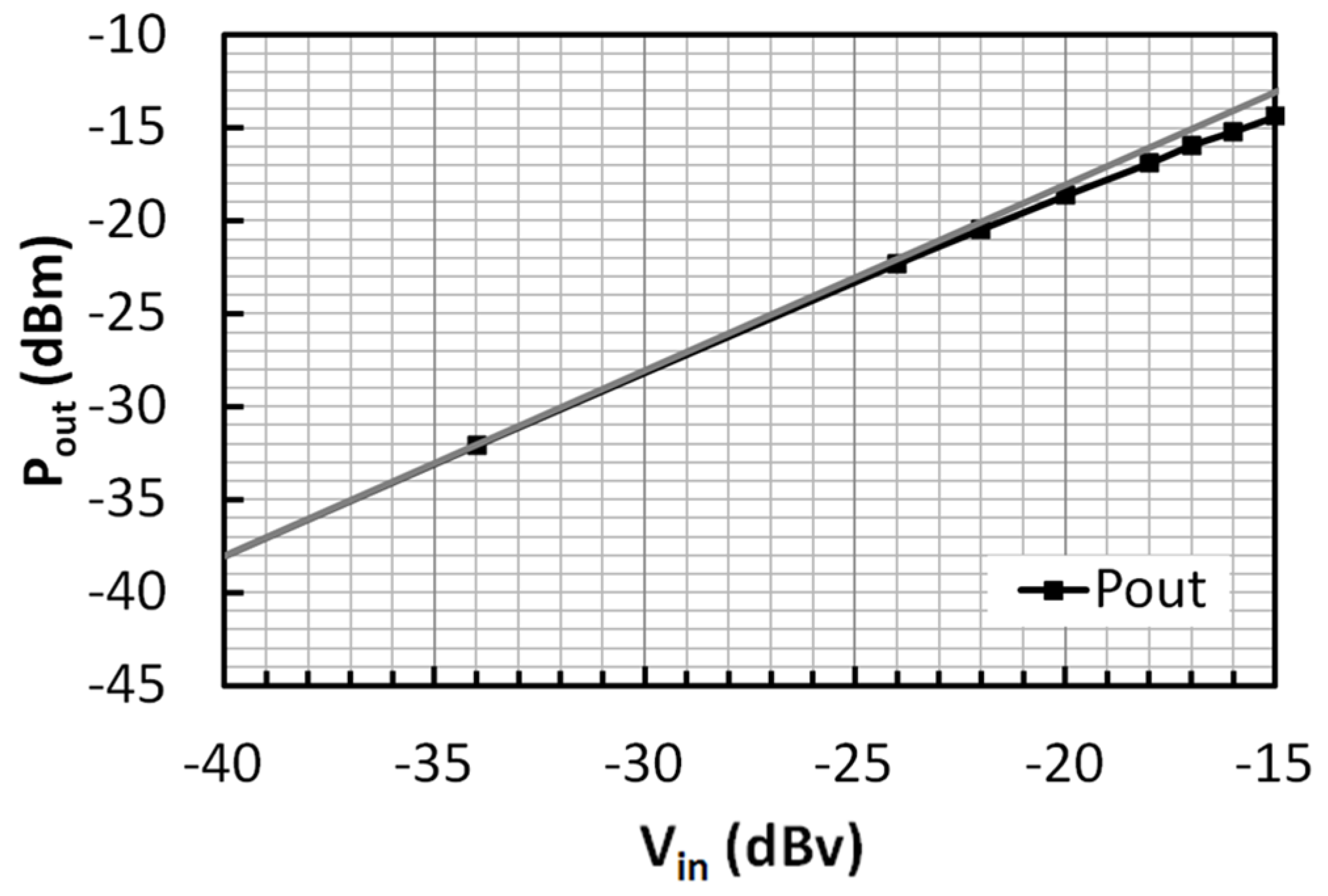
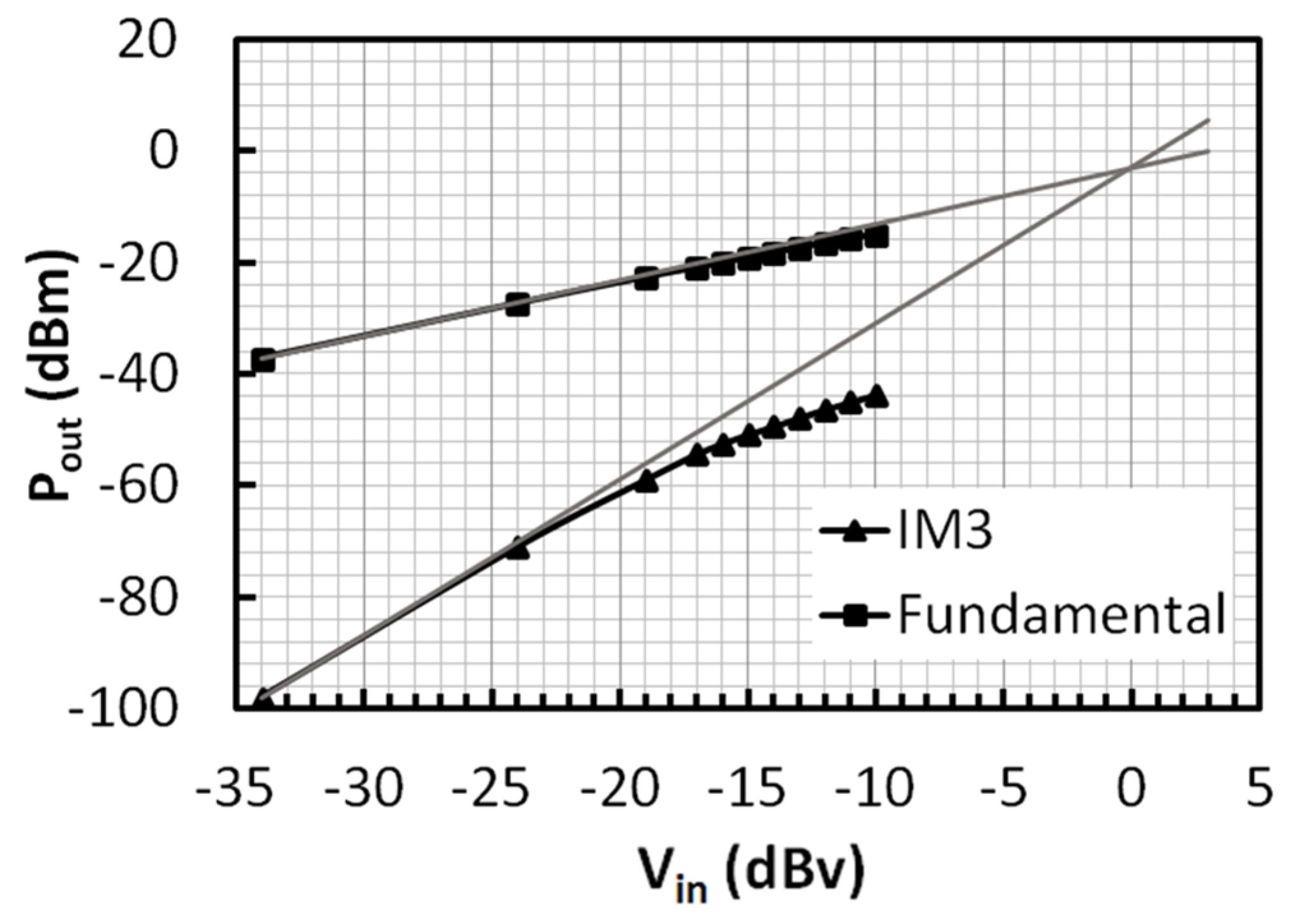
Figure 13a shows the output spectrum of SSF-LPF for an input swing of 0.5 Vpeak-to-peak at 100 MHz, where the level of the fundamental tone is −10.49 dBm and that of the third order harmonic is −51.81 dBm. Considering the cable losses of 0.22 dB and 0.49 dB at 100 MHz and 300 MHz, respectively, the third-order rejection is −41.05 dBc. Figure 13b shows the output spectrum of SSF-LPF for an input swing of 0.5 Vpeak-to-peak at 500 MHz, where the level of the fundamental tone is −13.14 dBm and that of the third order harmonic is −42.12 dBm. Considering the cable losses of 0.62 dB and 1.15 dB at 500 MHz and 1.5 GHz, respectively, the third-order rejection is −28.45 dBc. Figure 13c shows the output spectrum of SSF-LPF for an input swing of 0.5 Vpeak-to-peak at 1 GHz, where the level of the fundamental tone is −18.59 dBm and that of the third order harmonic is −53.68 dBm. Considering the cable losses of 0.89 dB and 1.66 dB at 1 GHz and 3 GHz, respectively, the third-order rejection is −34.32 dBc. Notably, the measurement is performed in a single-ended fashion by probing only one of the pseudo differential outputs, so the second order harmonic can be seen during the measurement. Figure 14 shows the measurement result of 1-dB compression point at 100 MHz, where the input voltage is swept from −40 to −15 dBv. The measured input 1-dB compression point of the 4th Elliptic LPF is −16.5 dBv. Figure 15 shows the measurement result of IIP3 with the two-tone signals at 100 MHz and 110 MHz. The measured IIP3 is −1 dBv.
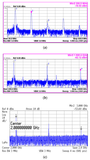
Figure 13.
(a) Measured output spectrum for the input of 0.5 Vpeak-to-peak @ 100 MHz. (b) Measured output spectrum for the input of 0.5 Vpeak-to-peak @ 500 MHz. (c) Measured output spectrum for the input of 0.5 Vpeak-to-peak @ 1 GHz.
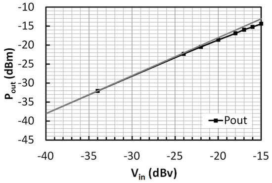
Figure 14.
Measured 1-dB compression point of the LPF at 100 MHz.
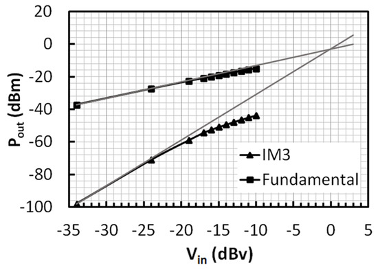
Figure 15.
Measured IIP3 of the LPF (for the two-tone signals at 100 and 110 MHz).
3.2. TX Analog Baseband
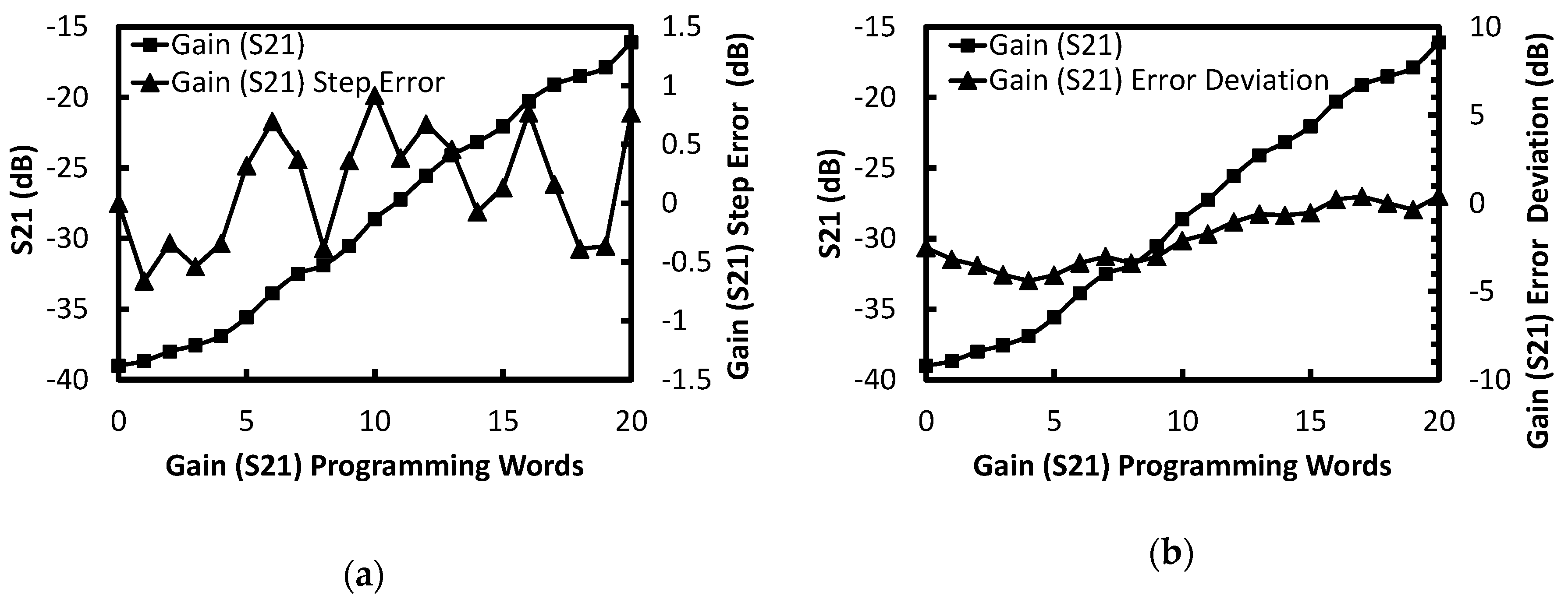
With the PGA operating in different gain modes, the S21 of the TX analog baseband are measured, as shown in Figure 16. The measured S21 is −16.26 dB in the highest gain mode and −39.67 dB in the lowest gain mode, which agrees well with the simulation results. According to the measurement results, the TX analog baseband exhibits the 3-dB bandwidth of 1.03 GHz in the highest gain mode and 1.05 GHz in the lowest gain mode. Figure 17a shows the measured S21 and gain step error. Figure 17b shows the measured S21 and gain error deviation. The achieved power gain range is from –39.67 dB to −16.26 dB, where the gain step error is −0.7 to +0.9 dB and the gain error deviation is −4.4 to +0.4 dB. The voltage gain range of −18.78–3.83 dB can be roughly estimated. The measured THD results versus the gain settings are shown in Figure 18, where the output signal level would be maintained at 200 mVpeak-to-peak during the measurement and the required input levels for different gain modes are calculated according to the measured gain. The measured THD is −10 dB in the lowest gain mode and −33.5 dB in the highest gain mode.

Figure 16.
Measured S21 of the TX analog baseband in different gain modes.

Figure 17.
(a) Measured gain and gain step error of the TX analog baseband. (b) Measured gain and gain error deviation of the TX analog baseband.
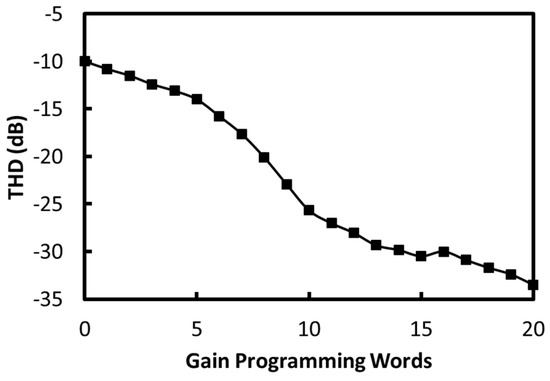
Figure 18.
Measured total harmonic distortion (THD) of the TX analog baseband in different gain modes.
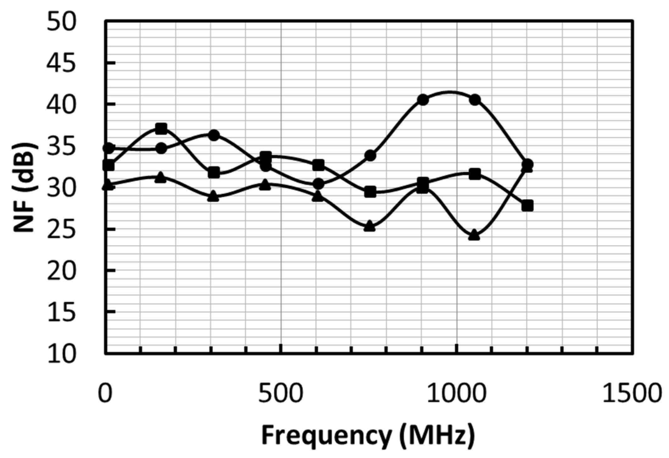
Figure 19 shows the IIP3 measurement result of the analog baseband. During the measurement, the input voltage is swept from −32 dBv to −4 dBv and the two-tone inputs are at 100 and 110 MHz. The TX analog baseband achieves the IIP3 of −0.2 dBv when the PGA operates in the highest gain mode. Figure 20 shows the measured 1-dB compression point of the TX analog baseband. During the measurement, the input voltage is swept from −40 to 5 dBv and the frequency of the input signal is 100 MHz. The circuit achieves the 1-dB compression point of −10 dBv when its PGA operates in the highest gain mode. The noise figure (NF) measurement results of three chip samples are shown in Figure 21. Again, the PGA operates in the highest gain mode during the measurement. Over the frequency range from 10 MHz to 1.2 GHz, the noise figures of 30.4–40.6 dB, 24.4–32.5 dB, and 27.8–37.0 dB are observed from the three chip samples of the transmitter analog baseband. The performance of the TX analog baseband is listed and compared with those of previous reported analog baseband circuits in Table 2 [10,11,12]. The TX analog baseband in this work achieves the wide bandwidth of 1.03–1.05 GHz and its noise figure and linearity are comparable with those of previous works.
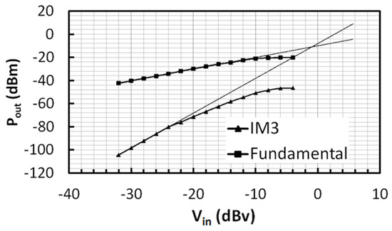
Figure 19.
Measured IIP3 of the TX analog baseband (for the two-tone inputs at 100 and 110 MHz).
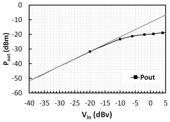
Figure 20.
The measured 1-dB compression point of the TX analog baseband.

Figure 21.
Noise figure measurement results of the TX analog baseband from three chip samples.
Table 2.
Performance Summary and Comparison.
4. Conclusions
The transmitter analog baseband consisting of the fourth-order Elliptic LPF and PGA is designed and implemented using 90-nm CMOS technology. For the requirement of adjacent channel rejection at 2.2 GHz, the transfer function of the SSF-based LPF is newly derived to consider the transmission zero and a capacitor CZ is included to allocate the transmission zero at the desired frequency. The LPF achieves the variable bandwidth from 0.76 to 1.23 GHz, the variable transmission zero from 2.03 to 3.33 GHz, and a fixed transmission zero at 4.6 GHz. The TX analog baseband achieves the bandwidth of 1.03–1.05 GHz, the NF of 24.4–40.0 dB and the voltage gain range from −18.9 to 3.8 dB.
Author Contributions
Conceptualization, H.-C.C.; Investigation, Y.-L.W. and C.-Y.C.; Supervision, H.-C.C.; Visualization, M.-Y.Y.; Writing—original draft, Y.-L.W. and C.-Y.C.; Writing—review & editing, H.-C.C.
Funding
This work was funded by MediaTek and the Ministry of Science and Technology, Taiwan, under the contract number MOST 105-2622-8-002-002.
Acknowledgments
We want to appreciate National Chip Implementation Center of Taiwan for the technical support during the chip fabrication.
Conflicts of Interest
The authors declare no conflict of interest.
References
- Osseiran, A.; Boccardi, F.; Braun, V.; Kusume, K.; Marsch, P.; Maternia, M.; Queseth, O.; Schellmann, M.; Schotten, H.; Taoka, H.; et al. Scenarios for 5G mobile and wireless communications: the vision of the METIS project. IEEE Commu. Mag. 2014, 52, 26–35. [Google Scholar] [CrossRef]
- Wan, P.; Chiu, Y.; Lin, P. A 5.8-mW, 20-MHz, fourth-order programmable elliptic filter achieving over 80-dB IM3. In Proceedings of the IEEE Custom Integrated Circuits Conference 2010, San Jose, CA, USA, 19–22 September 2010; pp. 1–4. [Google Scholar]
- D’Amico, S.; De Matteis, M.; Baschirotto, A. A 6th-Order 100μA 280MHz Source-Follower-Based Single-loop Continuous-Time Filter. In Proceedings of the 2008 IEEE International Solid-State Circuits Conference-Digest of Technical Papers, San Francisco, CA, USA, 3–7 February 2008; pp. 72–596. [Google Scholar]
- De Matteis, M.; Pezzotta, A.; D’Amico, S.; Baschirotto, A. A 33 MHz 70 dB-SNR Super-Source-Follower-Based Low-Pass Analog Filter. IEEE J. Solid-State Circuits 2015, 50, 1516–1524. [Google Scholar] [CrossRef]
- Elwan, H.; Tekin, A.; Pedrotti, K. A Differential-Ramp Based 65 dB-Linear VGA Technique in 65 nm CMOS. IEEE J. Solid-State Circuits 2009, 44, 2503–2514. [Google Scholar] [CrossRef]
- Kim, H.; Park, Y.; Yang, H.; Kim, S. A constant bandwidth switched-capacitor programmable-gain amplifier utilizing adaptive miller compensation technique. In Proceedings of the 2017 30th IEEE International System-on-Chip Conference (SOCC), Munich, Germany, 5–8 September 2017; pp. 249–252. [Google Scholar]
- Oneţ, R.; Neag, M.; Kovács, I.; Ţopa, M.D.; Rodriguez, S.; Rusu, A. Compact Variable Gain Amplifier for a Multistandard WLAN/WiMAX/LTE Receiver. IEEE Trans. Circuits Syst. Regul. Pap. 2014, 61, 247–257. [Google Scholar]
- Chen, Z.; Zheng, Y.; Choong, F.C.; Je, M. A Low-Power Variable-Gain Amplifier with Improved Linearity: Analysis and Design. IEEE Trans. Circuits Syst. Regul. Pap. 2012, 59, 2176–2185. [Google Scholar] [CrossRef]
- Kang, S.-Y.; Ryu, S.-T.; Park, C.-S. A Precise Decibel-Linear Programmable Gain Amplifier Using a Constant Current-Density Function. IEEE Trans. Microwave Theory Tech. 2012, 60, 2843–2850. [Google Scholar] [CrossRef]
- D’Amico, S.; Spagnolo, A.; Donno, A.; Chironi, V.; Wambacq, P.; Baschirotto, A. A low-power analog baseband section for 60-GHz receivers in 90-nm CMOS. IEEE Trans. Microwave Theory Tech. 2014, 62, 1724–1735. [Google Scholar] [CrossRef]
- Kumar, T.B.; Ma, K.; Yeo, K.S. A 4 GHz 60 dB Variable Gain Amplifier With Tunable DC Offset Cancellation in 65 nm CMOS. IEEE Microwave Wireless Compon. Lett. 2015, 25, 37–39. [Google Scholar] [CrossRef]
- He, L.; Li, L.; Wu, X.; Wang, Z. A Low-Power Wideband dB-Linear Variable Gain Amplifier With DC-Offset Cancellation for 60-GHz Receiver. IEEE Access 2018, 6, 61826–61832. [Google Scholar] [CrossRef]


© 2019 by the authors. Licensee MDPI, Basel, Switzerland. This article is an open access article distributed under the terms and conditions of the Creative Commons Attribution (CC BY) license (http://creativecommons.org/licenses/by/4.0/).