Article

Design and Emulation of All-Digital Phase-Locked Loop on FPGA

Graduate School of Engineering, Osaka University, Suita-shi, Osaka 565-0871, Japan
*
Authors to whom correspondence should be addressed.
Electronics 2019, 8(11), 1307; https://doi.org/10.3390/electronics8111307
Submission received: 14 October 2019 / Accepted: 5 November 2019 / Published: 7 November 2019
(This article belongs to the Section Circuit and Signal Processing)

Abstract

:
This paper demonstrates the design and implementation of an all-digital phase-locked loop (ADPLL) on Field Programmable Gate Array (FPGA). It is useful as an emulation technique to show the feasibility and effectiveness of the ADPLL in the early design stage. A Δ - Σ modulator (DSM, Delta-Sigma Modulator)-based digitally controlled ring-oscillator (ring-DCO) design, which is fully synthesizable in Verilog HDL, is presented. This ring-DCO has fully digital control and fractional tuning range using the DSM. The ring-DCO does not contain library-specific cells and can be synthesized independently of the standard cell library, thus making the design portable and reducing the time required to fit for different semiconductor processes considerably. Implemented ring-DCO has a wide tuning range and high-frequency resolution which meet the demands of system-level integration. The ADPLL implemented in this work has the characteristics of design flexibility, a wide range of working frequency from 120 MHz to 300 MHz, and a fast response for achieving a locked state. The proposed ADPLL can be easily ported to different processes in a short time. The design adaptation cost is limited to adjustment of loop parameters in the code. Thus, it can reduce the design time and design complexity of the ADPLL, making it very suitable for System-on-Chip (SoC) applications.

1. Introduction

The recent and ongoing explosive growth of wireless communication systems require low-cost, low-voltage, and low-power transceivers. To utilize the advantages of scalability and performance (unity current gain cut-off frequency and noise figure), integration of RF and analog circuits with digital circuits in the advanced Complementary Metal-Oxide-Semiconductor (CMOS) technology is promising, even under 0.5 V supply [1,2]. Even using a matured CMOS process, low-voltage operation RF and analog circuits are important and attract some interest, especially in wireless sensor applications with requirements of long battery lifetime. However, the shrinking voltage headroom is still one of the serious issues. For example, in phase-locked loops (PLLs), which are essential functional blocks to generate the local oscillator signal for modulation and demodulation, a voltage-controlled oscillator (VCO) is used. A VCO operating under 0.5 V supply can be realized [3], however, the range of control voltage is usually limited by the supply voltage, resulting in limitation of tuning range. Although combining discrete and continuous tuning can increase tuning range effectively [4,5], digital control tuning is an essential solution. Therefore, digitally controlled oscillator (DCO) and PLL using it, so-called all-digital PLL (ADPLL), are promising techniques for low-voltage accurate frequency generation [6,7,8,9].
On the other hand, such new circuit techniques are being actively sought since they achieve high levels of integration and low-power operation, while still meeting the stringent performance requirements of today’s wireless systems. Traditional phase-domain models of conventional charge-pump PLL [10,11] can give an analogy for the ADPLL design [12]. However, as well as fractional-N PLLs with high-resolution frequency resolution and relatively fast settling [13,14,15], typical DCOs use Δ - Σ modulation for precise frequency tuning. Even in steady-state, ADPLLs using them show dynamic variations in DCO tuning code, which is difficult to take into account in the conventional phase-domain PLL models. To deal with such complicated behaviors, a model-based analysis is often used [15,16] because transistor-level circuit simulations for PLL take a too long time. However, in this design methodology, transistor-level circuit design and model-based analysis are often iteratively carried out to meet some PLL performance requirements.
Fortunately, from a circuit-level point of view, ADPLLs are digital systems, and most of the digital functional blocks can be emulated on Field Programmable Gate Arrays (FPGA). Conventional charge-pump PLLs have a phase-frequency detector (PFD), charge pump, an analog loop filter, and a VCO. In typical ADPLLs, a time-to-digital converter (TDC), a digital loop filter, and a DCO replace the PFD, the analog loop filter, the VCO, respectively. Although the TDC can be implemented on FPGA [17], non-linearity due to signal distribution must be calibrated to an extent, resulting in design complexity. The controller-based ADPLLs reported in the previous works [9,18] avoid using TDCs and use a PFD, which is convenient in the FPGA emulation. This paper demonstrates the design and implementation of the TDC-less controller-based ADPLL on FPGA.
Some previous works on the FPGA emulation implemented DCOs by using a digital-to-analog converter converting a digital code into the oscillation frequency, or a counter, since analog functions cannot be implemented easily in FPGA [19,20,21]. In this work, a digitally controlled ring-oscillator (ring-DCO) is implemented for higher-frequency output, which is fully synthesizable by using Verilog HDL. This feature is useful for the top-down digital design approach because timing bottlenecks in the other digital circuits can be found at the FPGA emulation stage. The FPGA emulation can fill the gap between behavior-level and transistor-level simulations. It is noted that the digital circuits inside the ADPLL are not synchronous circuits operating at the same clock, but operate for multiple timing signals (DCO output, its frequency-divided signals, a reference signal, and PFD outputs).
This work is not targeting a final PLL based on Application-Specific Integrated Circuit (ASIC). As mentioned above, design and analysis in the early emulation phase of an ASIC-based PLL are focused. Design consideration, parameter selection, and optimization are studied along with the FPGA emulation techniques. Absolute performance cannot be set due to the limited performance of the FPGA. As described in [20], parameter scalability must be used.
This paper is organized as follows: In Section 2, the controller-based ADPLL and its functional building blocks are described. Section 3 shows a real-time LabVIEW FPGA emulation setup. Section 4 shows verifications about the functionality of the ADPLL. Section 5 draws the conclusions.

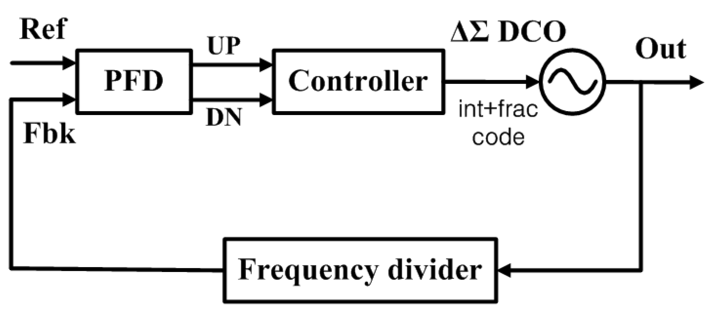
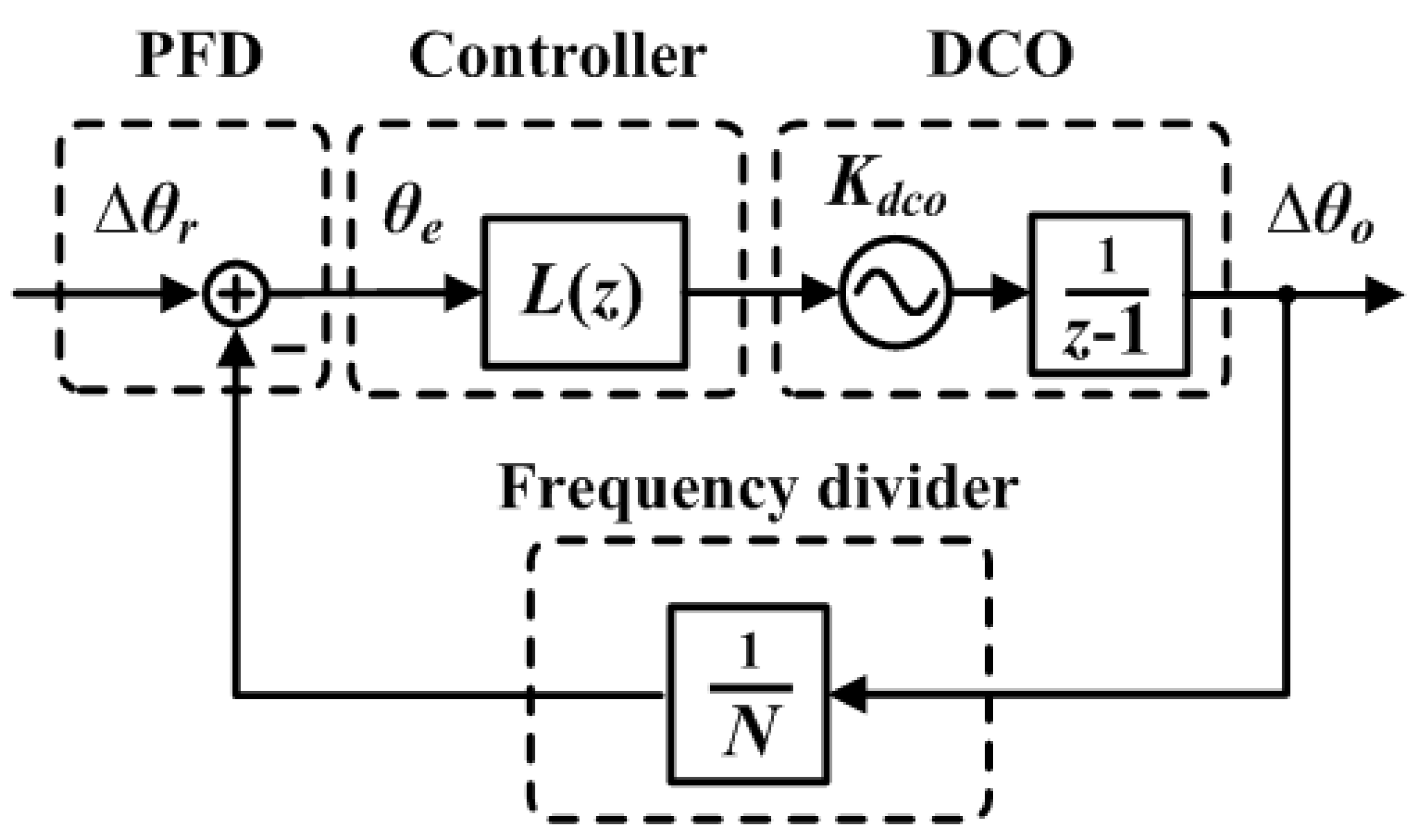
2. Controller-Based ADPLL and Its Functional Building Blocks

2.1. System Configuration
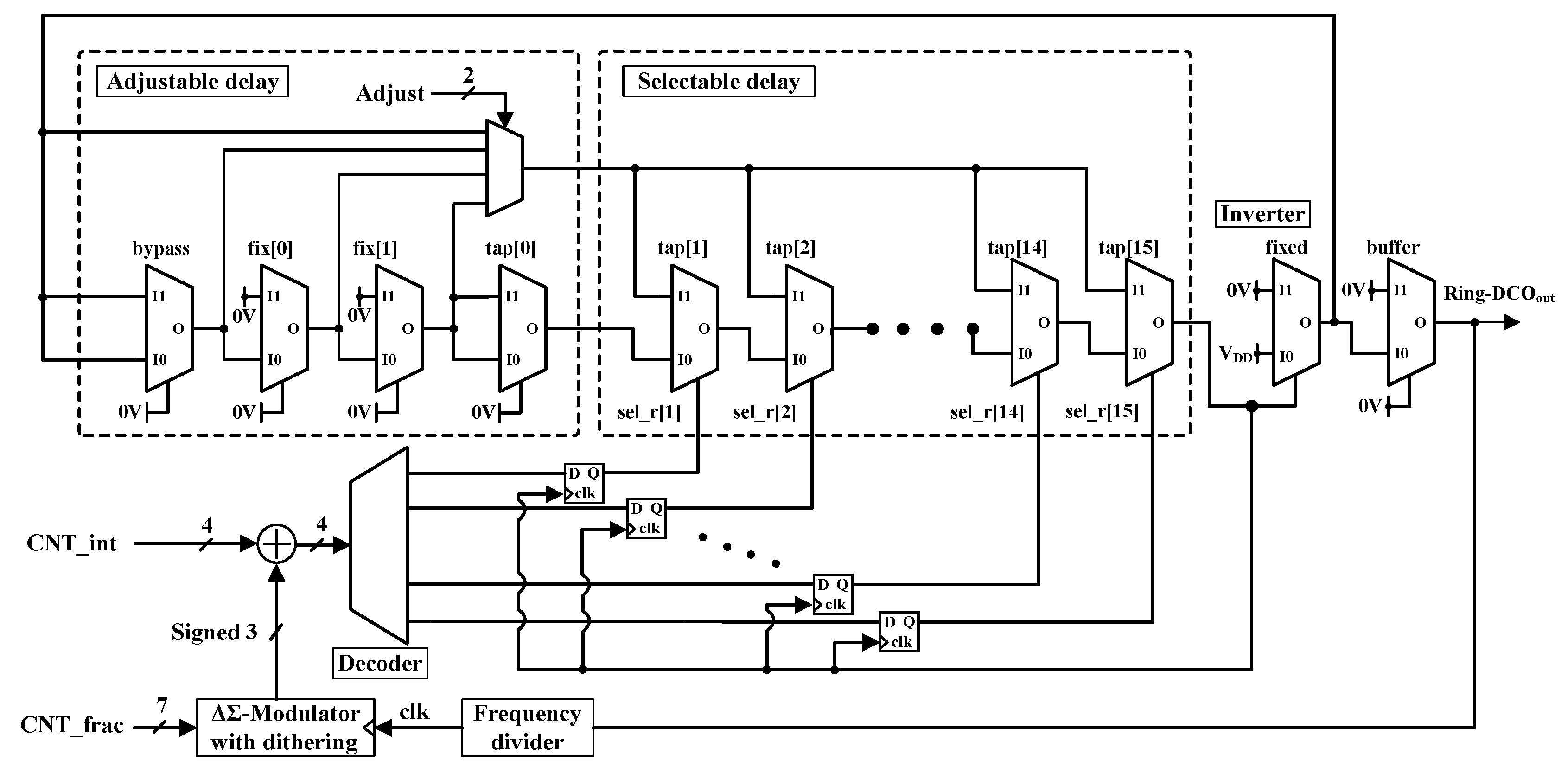
The structure of the ADPLL implemented is shown in Figure 1. It has four major building blocks: PFD, controller, ring-DCO, and frequency divider. The PFD detects both the phase and frequency differences between the two input signals. The pulses appear at UP, and DN relates to phase difference as in the conventional analog PLL. The controller which can realize a function of a charge pump and a loop filter accumulates the amount of these pulses at the rate of divided frequency of the ring-DCO output, and generates a frequency control code to tune the ring-DCO frequency at the rate of the reference signal. Compared with the previous work using no TDC [22], which utilizes the difference in period instead of phase difference, this controller operates at the divided ring-DCO frequency for precise phase difference detection.
Figure 2 shows the z-domain model of the ADPLL, where z = exp ( s / f r e f ) and f r e f is reference frequency.

2.2. Ring-DCO

A ring-DCO with the third-order Δ - Σ modulator (DSM, Delta-Sigma Modulator) is shown in Figure 3. The ring-DCO embeds some digital blocks for precise frequency tuning. The oscillation frequency is controlled through the digital logic blocks with two types of digital words (CNT_int and CNT_frac). A third-order feed-forward type DSM which can reduce the noise spur is utilized for precise frequency resolution. The noise transfer function N T F ( z ) of the employed modulator is given by [8,14]
N T F ( z ) = ( 1 z 1 ) 3 1 z 1 + 0.5 z 2 0.1 z 3 ,
where clock frequency in the DSM is used in the above z. The integer tuning step with 4-bit resolution covers a broad frequency range with a calibration of the considerable frequency uncertainty and fractional frequency tuning for precise frequency change.
A ring-DCO is realized through loop feedback of the buffers and inverters, which act as delay elements with the delay time determining the oscillation period. This implementation suffers from insufficient frequency resolution originating in the delay elements. The use of DSM with dithering improves the oscillation frequency resolution by avoiding the instantaneous switching through some flip-flops (FFs). The basic unit of the logic part for ring-DCO realization on FPGA is a look-up table (LUT). It can be thought of as an asynchronous Read-Only Memory (ROM) whose output changes with respect to the inputs. As the LUT has a transmission delay, the ring oscillator can be constructed on the FPGA. We use a selector to select the number of delay stages in the loop. It is important to have fewer signal changes in the loop to reduce the effect of factors like glitch noise.
In the current realization, each delay element is connected to the MUXs which are switched individually. Each delay element can input either the pre-delay output or just bypass the input. The shortest loop is realized when all the stages are bypassed and connected to the last stage, while the most extended loop is formed by connecting all the delay elements in the loop. The selection of the number of delay stages can be changed through set value which is latched by the FFs to avoid oscillation waveform distortion.
One of the critical design considerations is the selection signal update timing. The switching of the delay line during signal change causes incorrect oscillation. To reduce the unwanted switching, when the signal change is passed through the selectable delay element, the selectable delay switching is also carried out. Moreover, for the fixed delay line, the number of the fixed delay elements can be adjusted a little to guarantee monotonic ring-DCO tuning characteristics without complicated ones caused by complicated element mapping on the FPGA. All unused delay lines bypassed are switched to the bypass side. It is recommended to reset the delay line at startup. To avoid unstable operation due to external noises, etc., if one of the input signals of the front stage inverter is inverted, the signal of the delay line is fixed as 0 or 1 and is initialized. The implemented delay line has fixed steps (typically two) plus variable 15 steps. It is assumed that the wiring delay of the delay lines are sufficiently smaller than the delay time of the delay line itself.

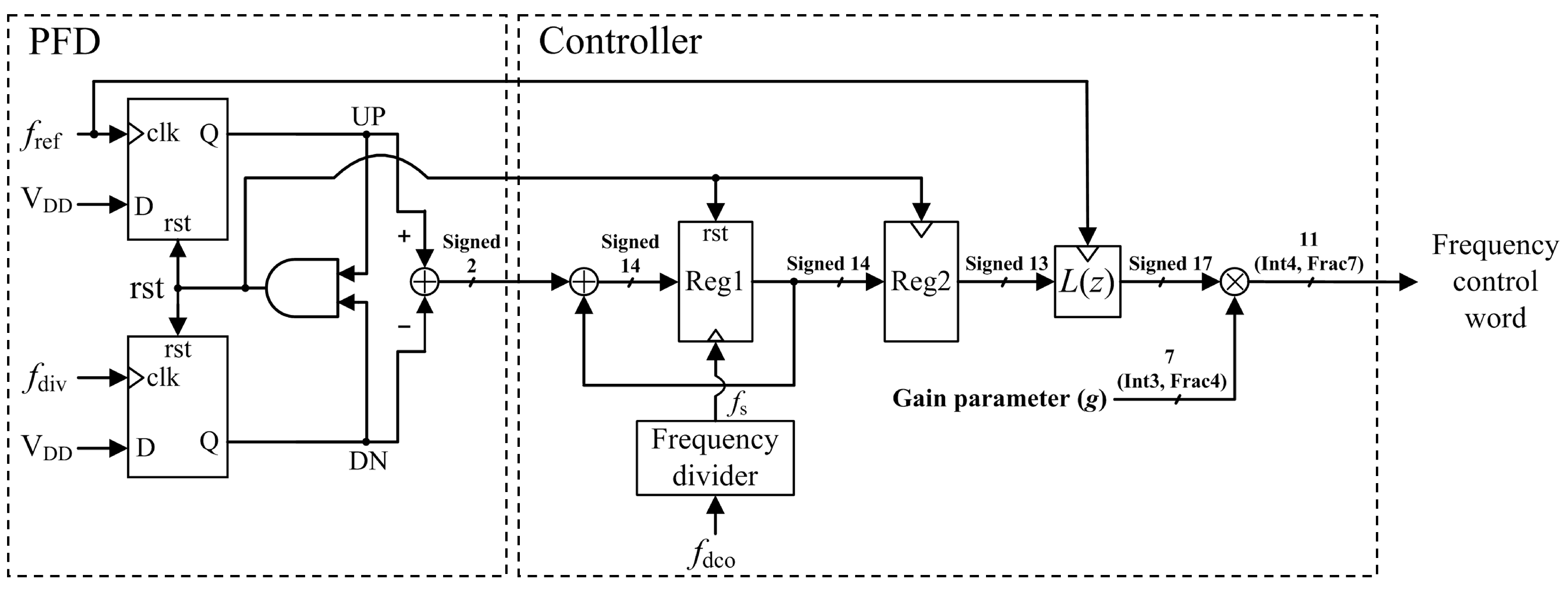
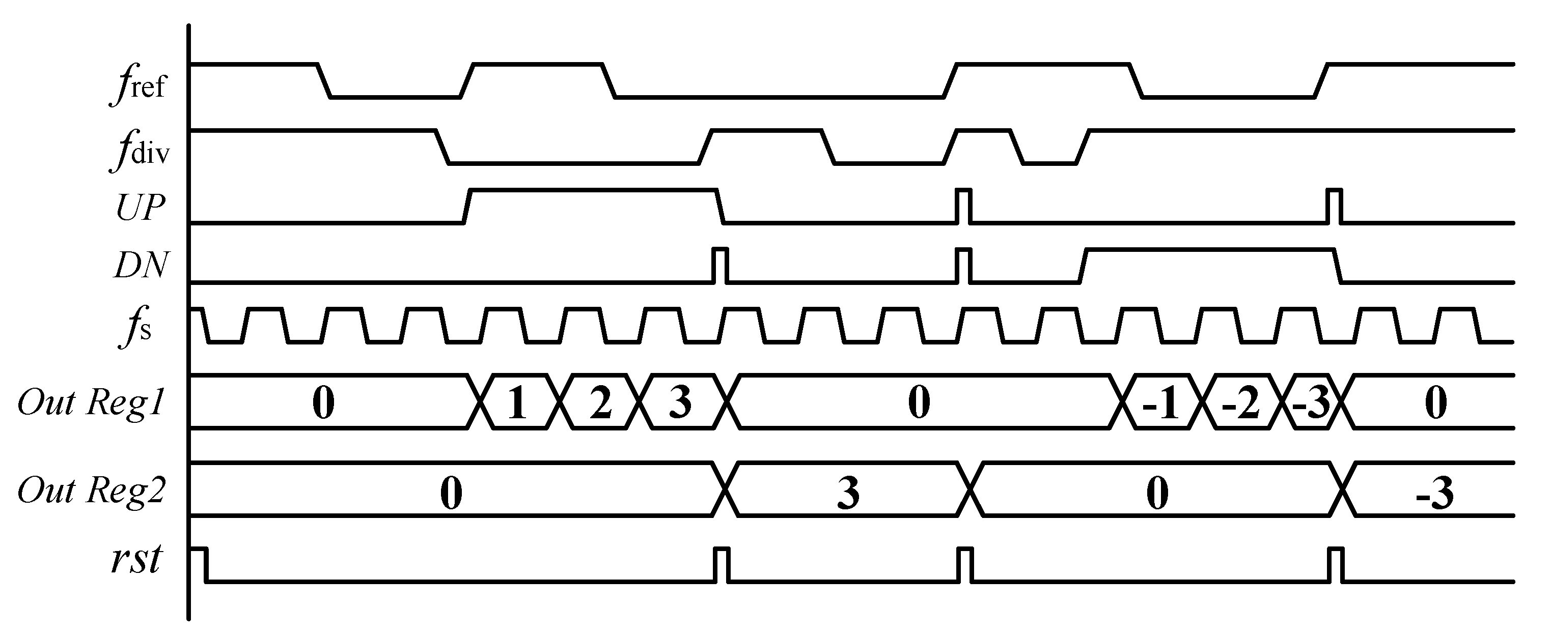
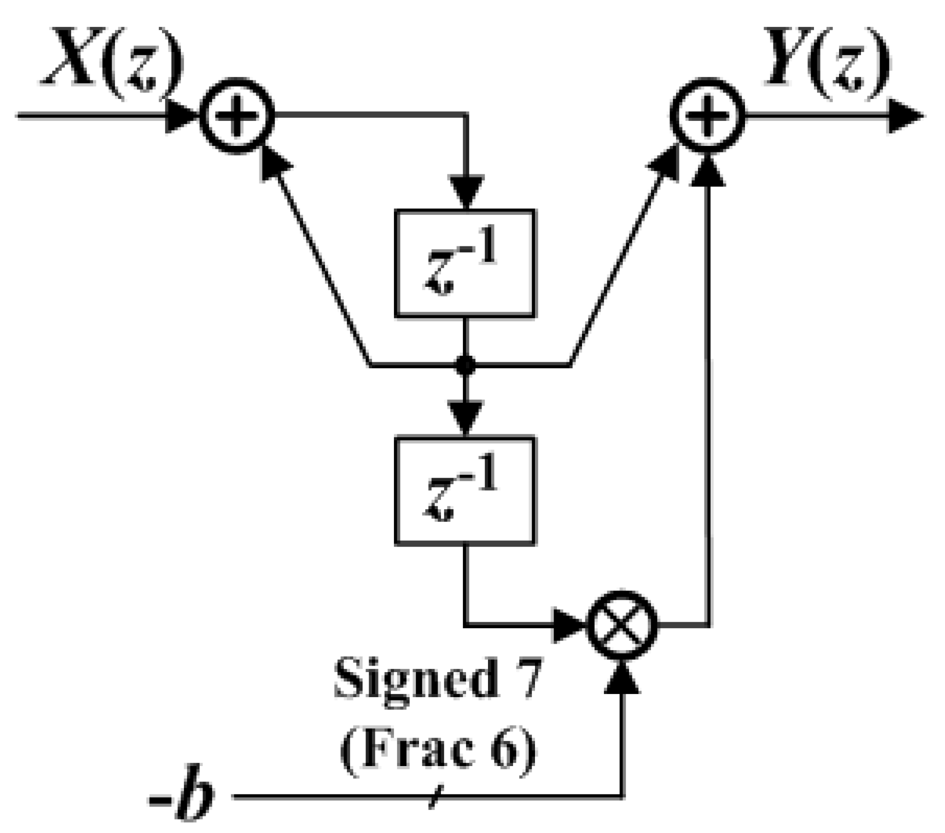
2.3. PFD and Loop Filter

In the typical ADPLL, TDC has been replacing conventional PFD and controller. However, TDC requires additional system complexity to achieve high resolution. Such a structure can increase the noise level and spur. Hence, TDC-less controller-based ADPLL is considered and designed using a fully synthesizable Verilog-HDL. The sampling rate for PFD outputs limits phase difference detection resolution, as described later.
The digital implementation of the loop filter is intended to emulate the response of the passive analog filter. The PFD and the loop filter are implemented using digital techniques, which have advantages over the analog designs. The loop filter parameters are numerical coefficients. They can be easily modified, and unlike an analog PLL, they have a more flexible limit to how large they can be. In addition, the digital phase detector does not suffer from thermal noise, degradation or drift, and charge pump mismatch or leakage. However, the quantization noise from the digital blocks is far higher than the conventional thermal noise. In this work, fixed-point digital implementation is used based on practical consideration. Some trade-offs exist between the granularity of the loop filter coefficients ( α 1 , ρ , and α 2 ) and the ideal response characteristics of the loop filter. One of these trade-offs is to constrain the parameters to satisfy the stability criterion of the closed-loop system which also puts a limitation on the loop bandwidth that can be accommodated. Detailed mathematical analysis and the empirical parameter approximations in terms of design parameters are carried out in the previous works [9,18].
As shown in Figure 4, the employed PFD consists of D-flip-flops and an AND gate in the feedback path for the reset. Figure 5 shows the timing diagram of the PFD inputs, UP and DN signals, and the accumulation register value based on the PFD reset and sampling clock. The PFD reset signal is used as the reset for the Reg1 value. The major contribution in the design is the PFD, which gives a numeric output. The PFD detects the phase error and converts it into a numeric value through the UP and DN signals. This allows the use of a digital filter as the loop regulator. The error signal is sampled by DCO clock divided by 4, 8, 16, 32, and 64 (set to 4 in the current implementation considering timing error) to measure the phase difference, which determines phase resolution. The sampled error signal is accumulated to obtain the phase error signal. Sampling rate f s is greater than the f r e f , which is established by IP core DSP48 as an accumulator considering high-speed operation in this work [23]. The PFD reset signal saves the contents of the counter (output of Reg1) into a register (output of Reg2). The IP core DSP48 can operate at faster clock than fabric designed one. It is useful to reduce the quantization noise of the phase error in this work. In this way, the larger the phase difference becomes, the larger the value the register saves, and the 13-bit number can be seen as a signed number, which provides information about the direction of the phase error as shown in Figure 5. When the value of “Out Reg1” may exceed the positive and negative range, it is clipped to the maximum positive or negative level by using additional logic circuits (not shown in Figure 4).
The loop filter L ( z ) samples the phase error signal and processes it at the reference frequency rate. As shown in Figure 4, multiplication by g parameter is applied after the loop filter to tune the open-loop gain of the ADPLL. In addition, multiplication by a scaling factor is hidden and is realized by assigning integer and fractional parts and truncating the lower fractional part. In this case, the scaling factor is B s c a l e = 2 13 .
In the previous works [9,18], the zero in the open-loop transfer function was introduced by using phase interpolation of the DCO output. In this study, phase interpolation does not have sufficient effect due to high DCO gain K d c o , and it is difficult to implement with digital elements. Instead of the phase interpolation, the loop filter is used to introduce zero in the open-loop transfer function in this study. This implementation is also useful to control the position of the zero dynamically. Transfer function L ( z ) of the loop filter shown in Figure 6, which is designed as a one-pole one-zero ( b 1 ) system in this study, is given by
L ( z ) = Y ( z ) X ( z ) = ( z b ) z 1 z 1 z b z 1 ,
where z = exp ( s / f r e f ) and can be approximated to unity in low frequency region ( | s / f r e f | 1 ). According to Figure 2, Figure 4, and Figure 6, the z-domain open-loop transfer function G ( z ) is expressed as:
G ( z ) = Δ θ o ( z ) / N θ e ( z ) = g ( z b ) N ( z 1 ) 2 K d c o K p f d B s c a l e ,
where K p f d is the PFD gain and ( N / 4 ) / 2 π in the case of f s = f d c o / 4 in Figure 4. Mathematically, the loop filter with two-pole and one-zero can be designed by introducing an additional pole. However, freedom of the parameters is too limited due to the discrete-time system nature (pole and zero frequencies in corresponding analog filter must be lower than f r e f / 2 ). Therefore, the above loop filter with one pole and one zero is used in this study. Besides the blocks shown in Figure 6, additional logic circuits are implemented to saturate the numeric results at every computational stage in case of overflow, as described before. This allows for the design to work even if the processed numeric values are too large, close to the limit of representation. In addition, the frequency control word (positive and negative) shown in Figure 4 is shifted up by a constant value to match the DCO input range (positive).
In the following sections, experimental setup and various measurements are carried out by varying the g, b, N parameters.

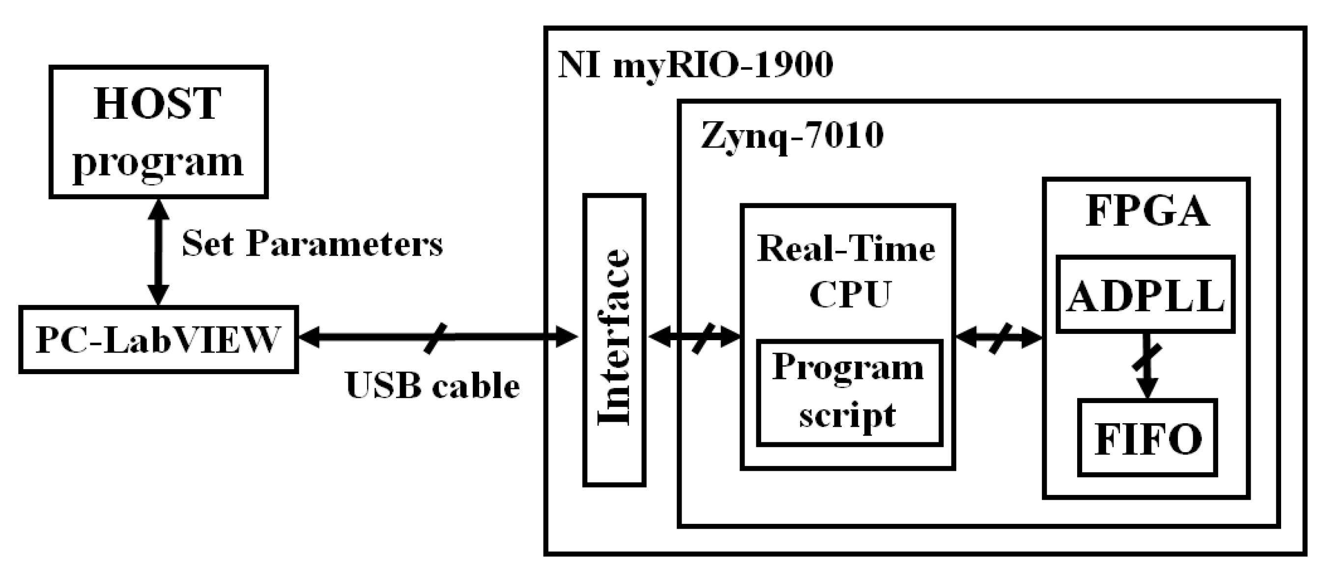
3. Experimental Setup

To demonstrate the effectiveness of FPGA emulation, the ADPLL system is designed mainly in Verilog. The FPGA used in this work is Xilinx Zynq 7010 on the NI myRIO-1900 board. Figure 7 shows the block diagram of the experiment setup. To confirm the ADPLL functionality, the design parameters of the ADPLL are set through the HOST program script programmed in NI LabVIEW, and the responses are measured and monitored from the real-time Central Processing Unit (CPU) on the board by a real-time program script. Some VHDL codes are also used to embed Verilog code in the LabVIEW system. The data about phase error and frequency control words are collected from FPGA first-in first-out (FIFO) memory at a sampling rate of 400 kHz and processed to confirm the ADPLL response.
The maximum DCO frequency in this work can exceed the maximum frequency of the FPGA digital I/O blocks which is specified by the board (NI myRIO-1900) [24]. This means that the DCO output cannot be observed by using external experimental equipment. Instead of this, the pulse counting technique, which was used for a built-in VCO auto-tuning function [5], was used inside the FPGA to obtain the DCO frequency approximately. The counter counts the pulses generated from the DCO over a specified period which uses a 40 MHz master clock divided by 2 16 . The counted value gives the averaged oscillation period. To operate only DCO in an experiment, some digital circuits to disconnect it from the loop filter and control it directly are embedded. Some frequency dividers and counters are established by using the binary counter IP core considering high-speed operation [25]. It is also convenient to keep sufficient number of programmable logic elements to implement the other logic circuits. Zynq 7010 is one of the smallest available FPGAs in terms of the amount of logic fabric. Table 1 gives the synthesis details and the power consumption estimation of the designed ADPLL. Considering the timing issue, an implementation strategy to optimize performance is adopted. The digital loop filter is dominant in the usage of resources due to its bit number. The power consumption for the system clock of 40 MHz is estimated by using Xilinx Power Estimator (XPE_2019.1.1). The ambient temperature of 25 C is set for the estimation with no heat sink and air flow of 250 Linear-Feet-per-Minute (LFM). Although some Zynq FPGA devices exist for more suitable resource utilization, the NI LabVIEW environment we use in this work gives constraints to select FPGA device.

4. Experimental Results

This section demonstrates ADPLL emulation results to reveal the feasibility of the FPGA emulation. It is noted that emulated results depend on the used FPGA and compilation technique. For example, if different FPGA (this means different fabrication process) is used, different DCO characteristics will be obtained due to its asynchronous nature depending on the delay element. Different FPGA in this work corresponds to different fabrication process in ASIC-based design. To reduce the variation of DCO characteristics among synthesis runs, some implementation constraints are set for some nets related to delay-elements. The following results are obtained for the same compiled FPGA.

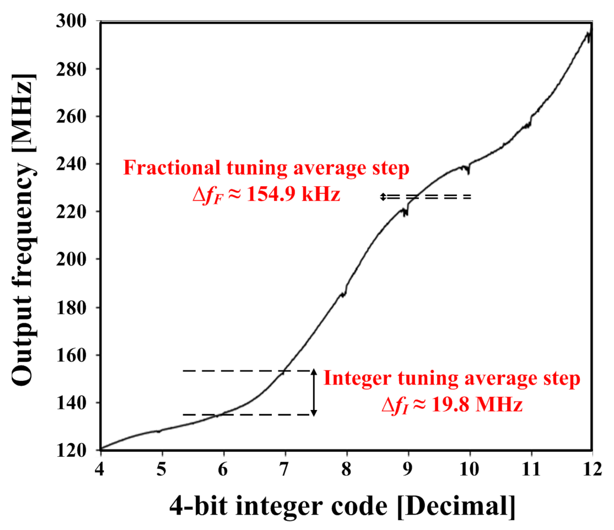
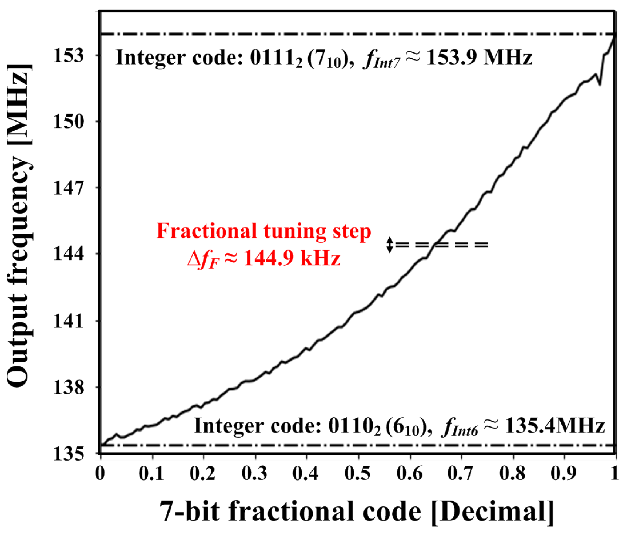
4.1. DCO Frequency Range

To confirm the DCO functionality for the frequency control word range of 4–12, an incremental step size of the 7-bit fractional code is used. The oscillator frequency is derived from integer and fractional frequency tuning steps. The frequency division ratio of the frequency divider in Figure 3 for the DSM is set 16. The output frequency is obtained by averaging the 10 data collected in the 100 ms time interval.
The implemented ring-DCO on FPGA has a tuning range of 120 to 300 MHz. The result of DCO tuning characteristics is shown in Figure 8 and Figure 9. The frequency resolution of the integer step is around 20 MHz. The 7-bit fractional frequency tuning steps to cover the narrower frequency range has a resolution of around 145 kHz. Some small oscillation frequency drops appear in this work, which originate due to instantaneous supply voltage drop caused by other digital circuits. It is inevitable in FPGA emulation where the supply voltage is shared for all circuits. This phenomenon is significant around the 4-bit integer change, which means many changes of the 7-bit fractional word. In this situation, it is attributed by the charging/discharging and short-circuit currents in digital circuits inside the DSM.

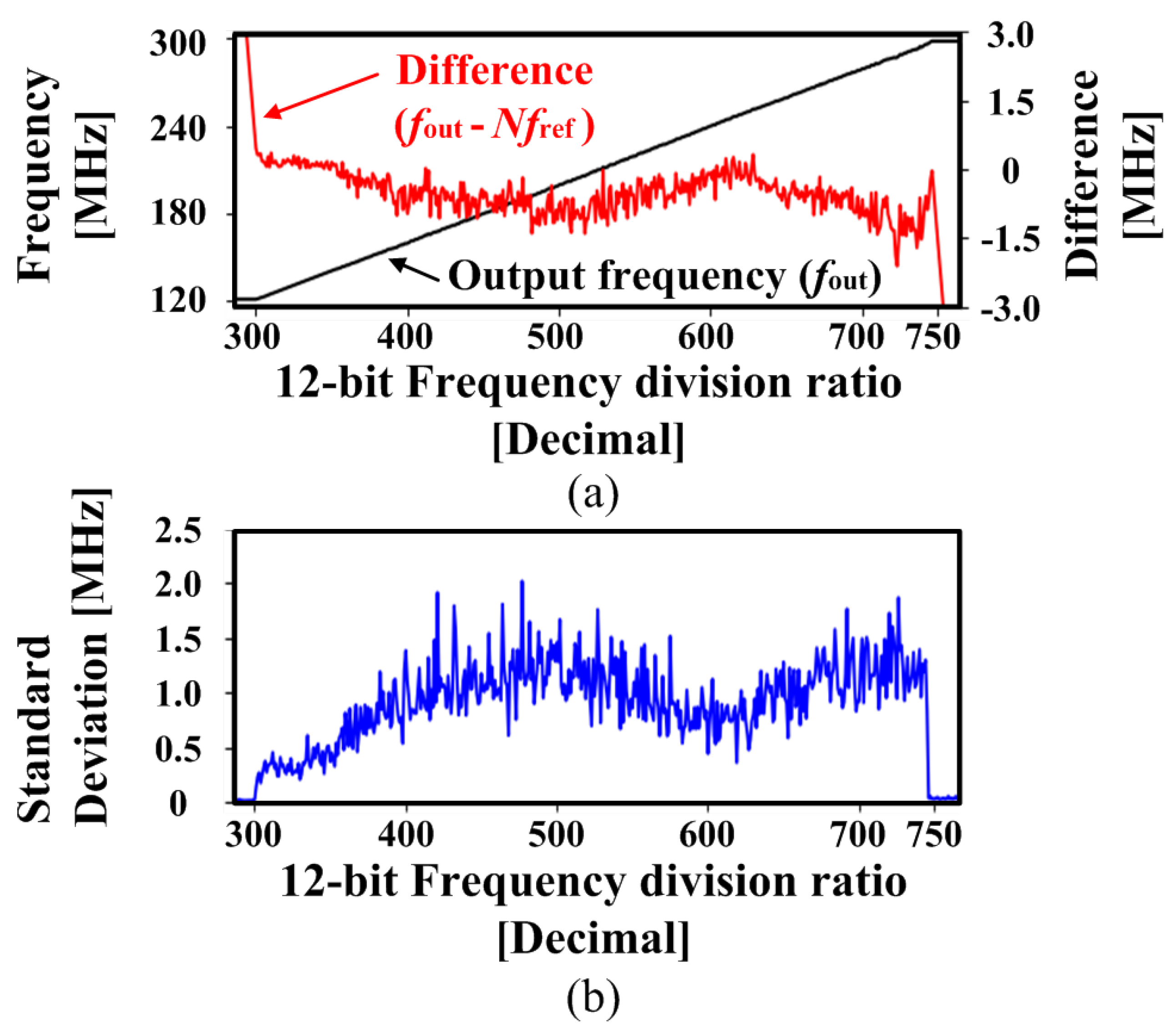
4.2. ADPLL Steady-State Operation

The steady-state ADPLL locking for parameter setting of b = 0 , g = 1 , and N varying from 300 to 750 is confirmed for an input reference frequency of 400 kHz, which is generated from the master clock in this work. Figure 10a shows the steady-state ADPLL frequency with clear linearity and its deviation from the ideal frequency corresponding to the frequency division ratio. The standard deviation of the frequency measurement is shown in Figure 10b which includes the influence of K d c o , DSM, and experimental setup. The frequency accuracy around ±0.5% is reasonable considering DCO frequency resolution and quantized PFD phase detection.

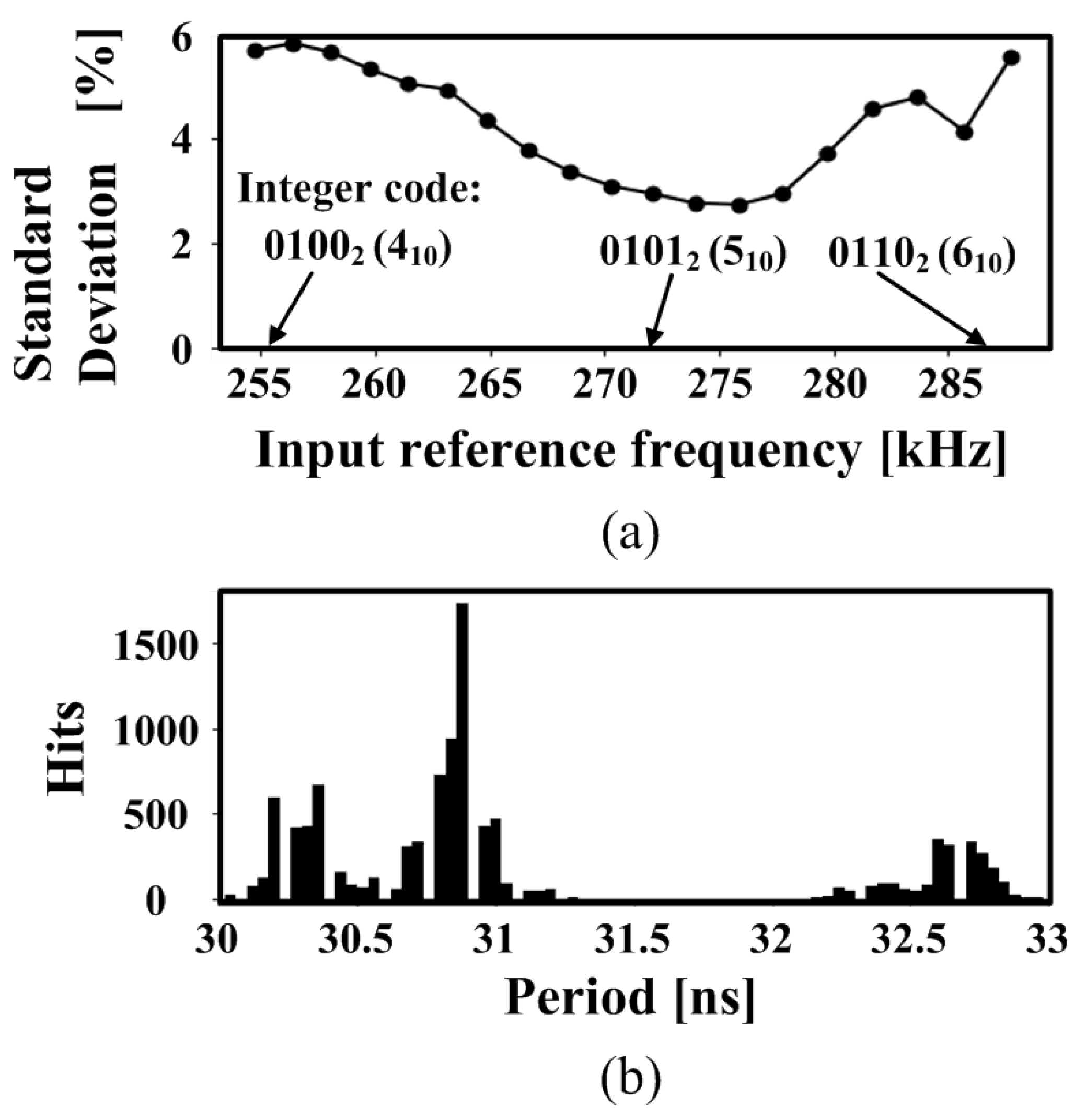
4.3. Jitter Measurement

Although the maximum frequency of the FPGA digital I/O is limited to 50 MHz, the actual jitter value of the ADPLL output can be estimated roughly by measuring its frequency-divided signal on digital I/O directly. The jitter dependency with the division ratio of the frequency divider on the f d c o signal shown in Figure 4 is confirmed roughly as inversely proportional to the square root of the division ratio. Figure 11 shows the jitter measurement results of the f s signal shown in Figure 4 (divided-by-4 ADPLL output) for the input reference frequencies in the range of 255 kHz to 288 kHz with a division ratio (N) as 472. In this work, 10,000 samples are obtained for each jitter histogram. Figure 11a shows the measured standard deviation (%) of the jitter with mean period on the steady-state ADPLL output signal divided by 4. The estimated jitter standard deviation of ADPLL output is estimated to be approximately a half of the value. The variation of the estimated jitter is attributed to the K d c o and the digital blocks in this implementation. Figure 11b shows the jitter histogram of the period with a input reference frequency as 272 kHz. The different peaks are due to the influence of digital blocks (DSM effect), and correspond to period for different instantaneous DCO control codes (CNT_int + signed 3-bit code from the DSM in Figure 3). To realize the third-order DSM, the single-loop structure with the noise transfer function N T F ( z ) given in Equation (1) is used in this work [8,14]. It has narrower output range than conventional multi-stage noise shaping (MASH) structure. This selection for the DSM structure is suitable for low jitter. If a ring-DCO with smaller K d c o is used at the expense of oscillation frequency, jitter would be reduced further.
Tektronix digital storage oscilloscope TDS6604 is used for the above jitter measurement. The storage memory size limits the sample number. To estimate bit error rate in practical communication applications, more samples may be required. However, 10,000 samples are sufficient to demonstrate the feasibility and usefulness of FPGA emulation in ADPLL design.
Although FPGA cannot emulate about phase noise of oscillator itself, the DCO with DSM has a lot of influence of quantization, as shown in Figure 11b, which periodic steady-state and noise analyses cannot simulate easily. Considering the advantage of the FPGA emulation on the DCO, it is important.

4.4. Input Frequency Step Response

The time-domain FPGA emulation cannot directly demonstrate frequency-domain characteristics (loop bandwidth, phase margin, etc.). However, based on conventional PLL theory, time-domain and frequency-domain responses are related through PLL parameters. Therefore, time-domain response is focused in this work.
By introducing a step change in the input reference frequency from 400 kHz to 272 kHz and vice versa with a division ratio (N) as 472, the ADPLL step response is measured at the output for different parameter settings. The frequency control word variation is measured, as well as the variation of phase error word normalized by N. From many data obtained for periodic step response, a median periodic response can be obtained, which can eliminate the influence of external noise originating in the experimental setup. In addition, they are processed with 5-point moving averaging to show the influence of ADPLL parameters (b and g). The timing in code variations is shifted to have the same 50% transition point of the frequency control code, as shown in the figures later.

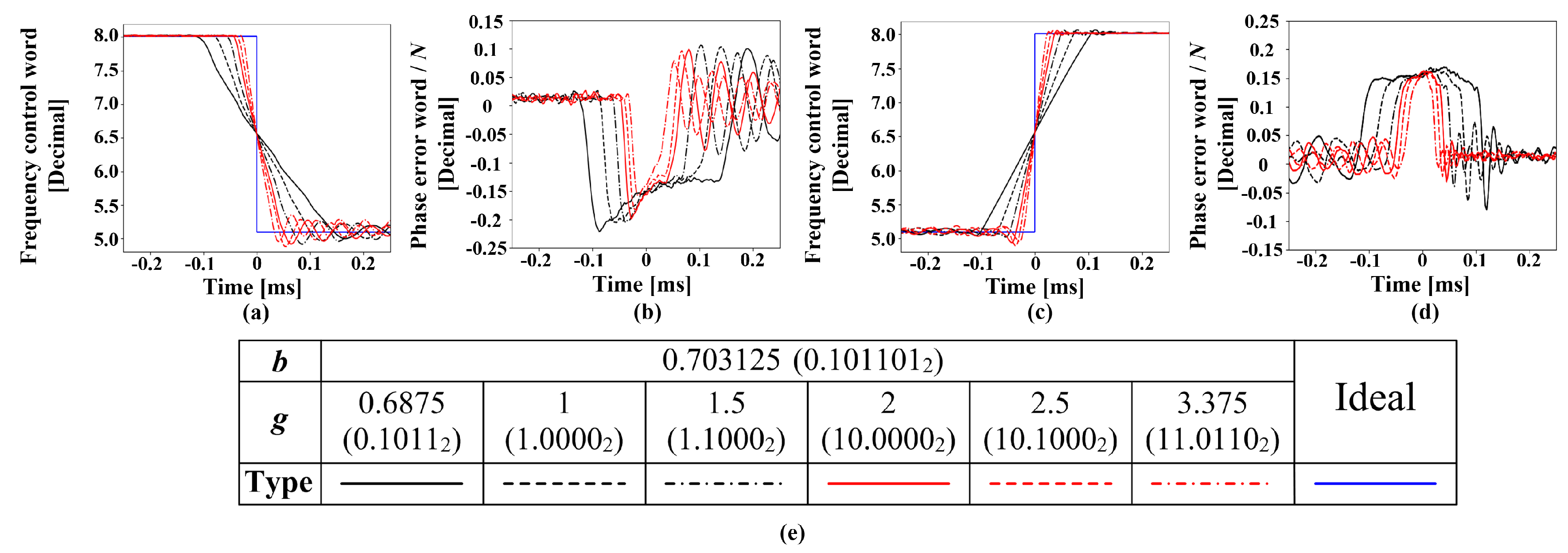
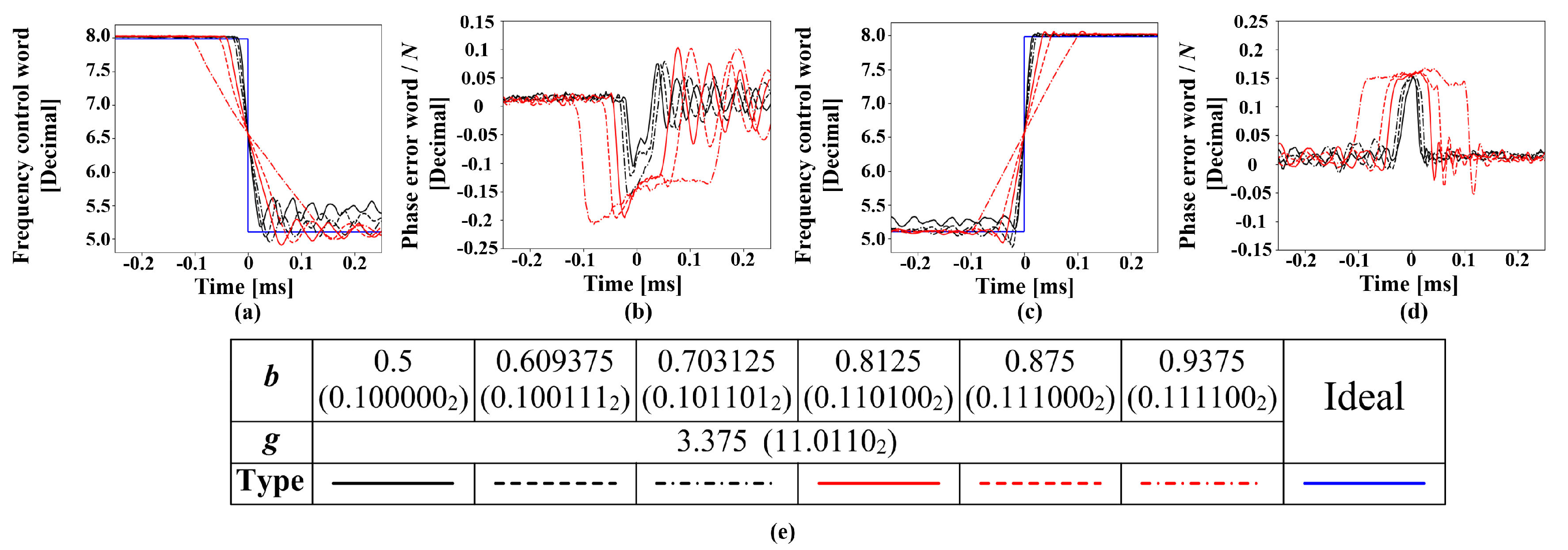
4.4.1. Influence of g Parameter with Fixed b Value

Figure 12 shows the ADPLL step response with the b parameter fixed to a value of 0.703125 (0.101101 2 ) and g varied from 0.6875 (0.1011 2 ) to 3.375 (11.0110 2 ). High gain parameter g for a fixed b parameter can enable fast code acquisition in the step response. According to the g parameter, response time changes from 200 μ s to 30∼50 μ s, as seen in Figure 12a,c. The code variations around the steady state depend on K d c o . It is noted that the variation of instantaneous DCO frequency with the DSM depends on K d c o . According to Equation (3), dependence of ADPLL frequency response on K d c o can be compensated with the g parameter. Therefore, small K d c o is better to reduce the variation of the instantaneous DCO frequency.
As periodic reference frequency change (both rising and falling in input frequency) is used, the positive time side of Figure 12a can connect to the negative time side of Figure 12c. In other words, residual error after the falling (rising) reference frequency change in Figure 12a (Figure 12c) corresponds to error before the rising (falling) reference frequency change in Figure 12c (Figure 12a). Thus, frequency control word converges to an extent, indicating loop stability. In the same way, residual error in phase error word also converges in average, but it fluctuates a lot, as seen in Figure 12b,d, which originates from DCO frequency variation described above.

4.4.2. Influence of b Parameter with Fixed g Value

As shown in Equation (3), the b parameter provides zero in the open-loop transfer function, which influences the ADPLL frequency step response. The ADPLL step response with the g parameter fixed to a value of 3.375 (11.0110 2 ) and b varied from 0.5 (0.1000 2 ) to 0.9375 (0.1111 2 ) is shown in Figure 13. For this specific g parameter, b parameter ranging from 0.5 to 0.703125 shows faster code acquisition. The response time changes from 200 μ s to 30∼50 μ s, as seen in Figure 13a,c. The loop is stable in this case, which is similar to the previous case (Figure 12).

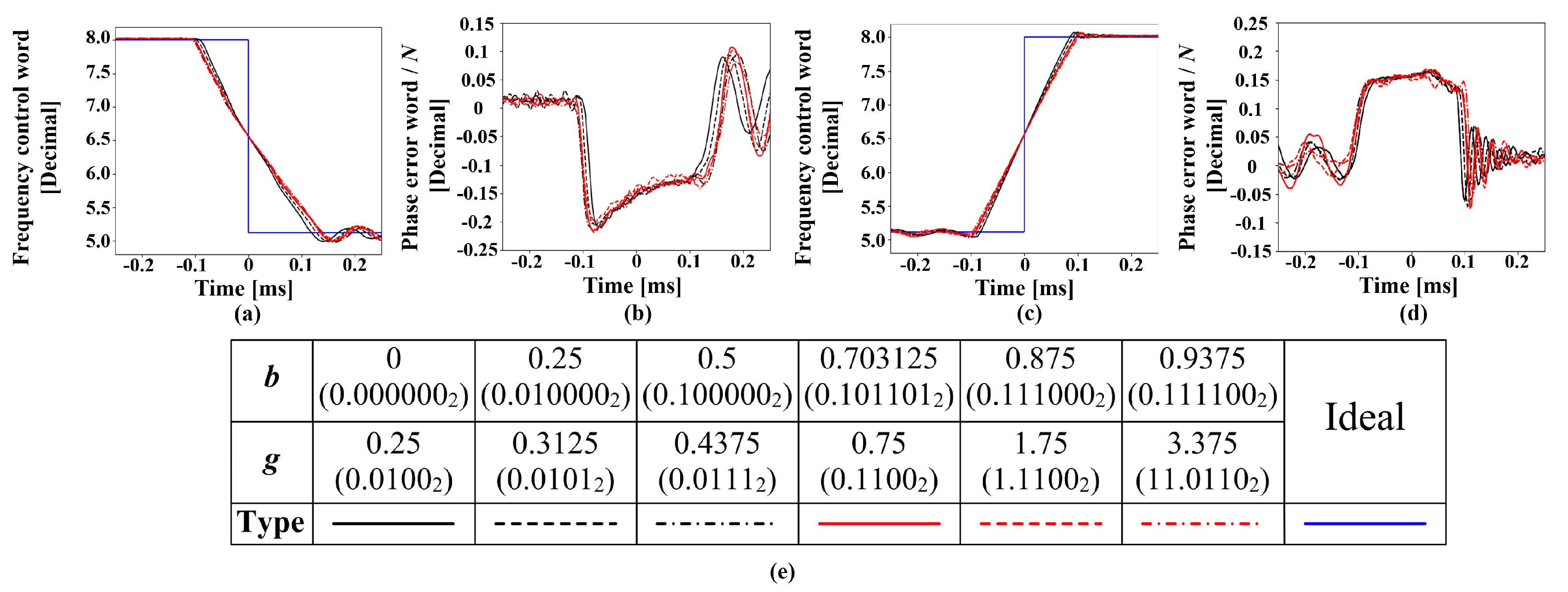
4.4.3. Case of Constant Low-Frequency Open-Loop Gain

According to Equation (3), the open-loop gain in low frequency ( z 1 ) has a factor of g ( 1 b ) . This indicates that some selections of g and b parameters can realize the same low-frequency open-loop gain. Figure 14 shows the ADPLL step response for some parameter selections, providing the low-frequency open-loop gain factor g ( 1 b ) near 1 / 4 . As seen in this figure, adequate selection of the b and g parameters for a constant low-frequency open-loop gain can realize a similar step response. The loop is stable in this case, which is similar to the previous cases (Figure 12 and Figure 13).

5. Conclusions

This paper proposes an ADPLL with good design efficiency and which has good portability over different processes. FPGA emulation shows the feasibility and effectiveness of the designed ADPLL. The proposed ADPLL emulation can reduce the design time and design complexity. Implemented ring-DCO has a wide tuning range and high-frequency resolution which meet the demands of system-level integration. The ADPLL implemented in this work has characteristics of its flexible design, a wide range of working frequency from 120 MHz to 300 MHz, and a fast response for achieving a locked state (typical response time around 30∼50 μ s).
The proposed ADPLL can be easily ported to different processes in a short time. The design adaptation cost is primarily limited to the adjustment of loop parameters in the code. To determine the ADPLL loop parameters, the nature of the discrete-time systems and quantization are often important. Although FPGA cannot emulate about phase noise of the oscillator itself well in real ASIC-based design, the FPGA emulation is useful to check a lot of influence of discrete-time nature and quantization in DCO with DSM in the early design stage, which periodic steady-state and noise analyses cannot simulate easily. It can fill the gap between behavior-level and transistor-level simulations. In early-stage design, FPGA emulation can reduce the number of design iterations, especially to check timing bottleneck in DSM, digital loop filter, and so on. Thus, it can reduce the design time and design complexity of the ADPLL, making it very suitable for System-on-Chip (SoC) applications.
Since the present study using a commercial FPGA board is still preliminary, an extensive future study is necessary. By developing the FPGA board with more suitable resource utilization for the ADPLL, the advantage of the FPGA emulation can be more obvious. In addition, considering the future of FPGA technology [26,27], which can contribute to filling the gap between FPGA and ASIC, the FPGA implementation of ADPLL also has feasibility as a real-operating PLL design.

Author Contributions

Conceptualization, S.R. and T.M.; methodology, software, and validation, S.R., T.Y. and T.M.; investigation, S.R.; writing—original draft preparation, S.R.; writing—review and editing, T.Y. and T.M.

Funding

This research received no external funding.

Acknowledgments

Saichandrateja Radhapuram would like to acknowledge Japan International Corporation Agency (JICA) for research fellowship (D-12-90401).

Conflicts of Interest

The authors declare no conflict of interest.

References

  1. Chen, H.-C.; Wang, T.; Chiu, H.-W.; Kao, T.-H.; Lu, S.-S. 0.5-V 5.6-GHz CMOS Receiver Subsystem. IEEE Trans. Microw. Theory Tech. 2009, 57, 329–335. [Google Scholar] [CrossRef] [Green Version]
  2. Matsuoka, T.; Wang, J.; Kihara, T.; Ham, H.; Taniguchi, K. Low-Voltage Wireless Analog CMOS Circuits toward 0.5 V Operation. IEICE Trans. Fundam. 2010, E93-A, 356–366. [Google Scholar] [CrossRef]
  3. Yamashita, F.; Matsuoka, T.; Kihara, T.; Takobe, I.; Park, H.-J.; Taniguchi, K. Analytical design of a 0.5V 5GHz CMOS LC-VCO. IEICE Electron. Express 2009, 6, 1025–1031. [Google Scholar] [CrossRef] [Green Version]
  4. Hegazi, E.; Sjöland, H.; Abidi, A.A. A Filtering Technique to Low LC Oscillator Phase Noise. IEEE J. Solid-State Circuits 2001, 36, 1921–1930. [Google Scholar] [CrossRef]
  5. Kamata, T.; Matsuoka, T.; Taniguchi, T. Design of Wideband Tuning VCO for TV Receiver System. IEICE Trans. Electron. Jpn. Ed. 2007, J90-C, 634–641. [Google Scholar]
  6. Staszewski, R.B.; Muhammad, K.; Leipold, D.; Hung, C.-M.; Ho, Y.-C.; Wallberg, J.L.; Fernando, C.; Maggio, K.; Staszewski, R.; Jung, T.; et al. All-Digital TX Frequency Synthesizer and Discrete-Time Receiver for Bluetooth Radio in 130-nm CMOS. IEEE J. Solid-State Circuits 2004, 39, 2278–2291. [Google Scholar] [CrossRef]
  7. Miyashita, D.; Kobayashi, H.; Deguchi, J.; Kousai, S.; Hamada, M.; Fujimoto, R. A −104 dBc/Hz In-Band Phase Noise 3 GHz All Digital PLL with Phase Interpolation Based Hierarchical Time to Digital Converter. IEICE Trans. Electron. 2012, E95-C, 1008–1016. [Google Scholar] [CrossRef]
  8. Bae, J.; Radhapuram, S.; Jo, I.; Kihara, T.; Matsuoka, T. A Design of 0.7-V 400-MHz Digitally Controlled Oscillator. IEICE Trans. Electron. 2015, E98-C, 1179–1186. [Google Scholar] [CrossRef]
  9. Bae, J.; Radhapuram, S.; Jo, I.; Wang, W.; Kihara, T.; Matsuoka, T. A Design of 0.7-V 400-MHz All-Digital Phase-Locked Loop for Implantable Biomedical Devices. IEICE Trans. Electron. 2016, E99-C, 431–439. [Google Scholar] [CrossRef]
  10. Gardner, F. Charge-Pump Phase-Lock Loops. IEEE Trans. Commun. 1980, 28, 1849–1858. [Google Scholar] [CrossRef]
  11. van Paemel, M. Analysis of a charge-pump PLL: A new model. IEEE Trans. Commun. 1994, 42, 2490–2498. [Google Scholar] [CrossRef]
  12. Kratyuk, V.; Hanumolu, P.K.; Moon, U.-K.; Mayaram, K. A Design Procedure for All-Digital Phase-Locked Loops Based on a Charge-Pump Phase-Locked-Loop Analogy. IEEE Trans. Circuits Syst. II 2007, 54, 247–251. [Google Scholar] [CrossRef] [Green Version]
  13. Riley, T.A.; Copeland, M.A.; Kwasniewski, T.A. Delta-sigma modulation in fractional-N frequency synthesis. IEEE J. Solid-State Circuits 1993, 28, 553–559. [Google Scholar] [CrossRef] [Green Version]
  14. Rhee, W.; Song, B.S.; Ali, A. A 1.1-GHz CMOS Fractional-N Frequency Synthesizer with a 3-b Third-Order ΔΣ Modulator. IEEE J. Solid-State Circuits 2000, 35, 1453–1460. [Google Scholar] [CrossRef]
  15. Perrott, M.H.; Trott, M.D.; Sodini, C.G. A Modeling Approach for Σ-Δ Fractional-N Frequency Synthesizers Allowing Straightforward Noise Analysis. IEEE J. Solid-State Circuits 2002, 37, 1028–1038. [Google Scholar] [CrossRef]
  16. Staszewski, R.B.; Fernando, C.; Balsara, P.T. Event-Driven Simulation and Modeling of Phase Noise of an RF Oscillator. IEEE Trans. Circuits Syst. I 2005, 32, 723–733. [Google Scholar] [CrossRef]
  17. Fishburn, M.; Menninga, L.H.; Favi, C.; Charbon, E. A 19.6 ps, FPGA-Based TDC With Multiple Channels for Open Source Applications. IEEE Trans. Nucl. Sci. 2013, 60, 2203–2208. [Google Scholar] [CrossRef]
  18. Radhapuram, S.; Bae, J.; Jo, I.; Wang, W.; Matsuoka, T. Analysis of A Controller-Based All-Digital Phase-Locked Loop. Far East J. Electron. Commun. 2015, 15, 57–73, Erratum in 2016, 16, 199–201. [Google Scholar] [CrossRef]
  19. Kumm, M.; Klingbeil, H.; Zipf, P. An FPGA-Based Linear All-Digital Phase-Locked Loop. IEEE Trans. Circuits Syst. I 2010, 57, 2487–2497. [Google Scholar] [CrossRef]
  20. Shan, C.; Zianbetov, E.; Yu, W.; Anceau, F.; Billoint, O.; Galayko, D. FPGA prototyping of large reconfigurable ADPLL network for distributed clock generation. In Proceedings of the 2013 International Conference on Reconfigurable Computing and FPGAs, Cancun, Mexico, 9–11 December 2013. [Google Scholar]
  21. Shan, C.; Zianbetov, E.; Anceau, F.; Billoint, O.; Galayko, D. A distributed synchronization of all-digital PLLs network for clock generation in synchronous SOCs. In Proceedings of the IEEE 13th International New Circuits and Systems Conference, Grenoble, France, 7–10 June 2015. [Google Scholar]
  22. Makihara, Y.; Ikebe, M.; Sano, E. Evaluation of Digitally Controlled PLL by Clocked-Period Comparison. IEICE Trans. Electron. 2007, E90-C, 1307–1310. [Google Scholar] [CrossRef]
  23. Xilinx. LogiCORE IP Accumulator v11.0 Product Specification; DS213 March 1; Xilinx: San Jose, CA, USA, 2011. [Google Scholar]
  24. National Instruments. NI myRIO-1900 User Guide and Specifications; National Instruments: Austin, TX, USA, 2016. [Google Scholar]
  25. Xilinx. LogiCORE IP Binary Counter v11.0 Product Specification; DS215 March 1; Xilinx: San Jose, CA, USA, 2011. [Google Scholar]
  26. Miyamura, M.; Sakamoto, T.; Bai, X.; Tsuji, Y.; Morioka, A.; Nebashi, R.; Tada, M.; Banno, N.; Okamoto, K.; Iguchi, N.; et al. NanoBridge-Based FPGA in High-Temperature Environments. IEEE Micro 2017, 37, 32–42. [Google Scholar] [CrossRef]
  27. Ochi, H.; Yamaguchi, K.; Fujimoto, T.; Hotate, J.; Kishimoto, T.; Higashi, T.; Imagawa, T.; Doi, R.; Tada, M.; Sugibayashi, T.; et al. Via-Switch FPGA: Highly Dense Mixed-Grained Reconfigurable Architecture with Overlay Via-Switch Crossbars. IEEE Trans. Very Large Scale Integr. (VLSI) Syst. 2018, 26, 2723–2736. [Google Scholar] [CrossRef]
Figure 1. The controller-based all-digital phase-locked loop (ADPLL) architecture.
Electronics 08 01307 g001
Figure 2. z-domain model of the controller-based ADPLL architecture. phase-frequency detector (PFD) gain ( K p f d ) and a scaling factor ( B s c a l e ), which are used in Equation (3), are not shown for simplification.
Electronics 08 01307 g002
Figure 3. Architecture of the digitally controlled ring-oscillator (ring-DCO) based on the third-order Δ - Σ modulator.
Electronics 08 01307 g003
Figure 4. Architecture of the PFD and controller.
Electronics 08 01307 g004
Figure 5. Timing diagram of the PFD and controller.
Electronics 08 01307 g005
Figure 6. Loop filter L(z) configuration.
Electronics 08 01307 g006
Figure 7. Block diagram of the experiment setup.
Electronics 08 01307 g007
Figure 8. Measured ring-DCO tuning characteristics.
Electronics 08 01307 g008
Figure 9. Measured ring-DCO tuning characteristics for fractional code range.
Electronics 08 01307 g009
Figure 10. Measured ADPLL: (a) frequency division ratio tuning frequency range and difference from ideal value, and (b) standard deviation.
Electronics 08 01307 g010
Figure 11. Measured jitter of the divided-by-4 ADPLL output signal: (a) standard deviation expressed as percentage of the mean value (10,000 samples), and (b) instantaneous period histogram for a input reference frequency of 272 kHz.
Electronics 08 01307 g011
Figure 12. Measured step response with b value fixed: (a,b) frequency control code and detected phase error code for falling input frequency step, (c,d) those for rising input frequency step, (e) the legend for each parameter. The timing in code variations is shifted so as to have the same 50% transition point of the frequency control code. The frequency control code is also shifted up to match the DCO input range.
Electronics 08 01307 g012
Figure 13. Measured step response with g value fixed: (a,b) frequency control code and detected phase error code for falling input frequency step, (c,d) those for rising input frequency step, (e) the legend for each parameter. The timing in code variations is shifted so as to have the same 50% transition point of the frequency control code. The frequency control code is also shifted up to match the DCO input range.
Electronics 08 01307 g013
Figure 14. Measured step response with low-frequency open-loop gain fixed: (a,b) frequency control code and detected phase error code for falling input frequency step, (c,d) those for rising input frequency step, (e) the legend for each parameter. The timing in code variations is shifted so as to have the same 50% transition point of the frequency control code. The frequency control code is also shifted up to match the DCO input range.
Electronics 08 01307 g014
Table 1. Synthesis details of designed ADPLL (Tool: Xilinx Vivado 2017.2).
ElementNumber (Utilization Rate)
Total Slices4310 (98.0%)
Slice LUTs13772 (78.2%)
Slice Registers13970 (39.7%)
Block RAMs10 (16.7%)
DSP48s4 (5.0%)
Power Consumption28 mW

