1. Introduction
With the rapid development of semiconductor and computer technology, embedded systems have achieved appearance in all spheres of our lives. The widespread usage and the exposure of the embedded system have made the embedded system security a prominent issue. Embedded systems are considered to be trusted in terms of architecture and hardware implementation, though there may be some security issues derived from the design stage. In recent years, the embedded systems are increasingly subjected to the adversaries that aim to get the private data of the users or control the behavior of the programs to perform malicious actions. The applications such as cell phones, wearable devices, financial terminals, industrial control systems, and military devices process and store a giant number of users’ critical information as they are providing users with convenience as well. In some of these critical scenarios, the security of the embedded devices must be treated additionally to provide secure execution of the applications.
Compared with the attacks on physical devices, software security exploits by the adversaries taken advantages of vulnerabilities in operating systems or applications is more widely used due to the fewer requirements of the victim hardware details. More and more vulnerabilities are exposed to attackers with the increased complexity of software design, which makes the minor malicious code and data hard to be detected. Malicious adversaries exploit to tamper program code and data, inject malicious code, and leak critical information. These attacks are easy to implement because most embedded programs are written in the unsafe program languages such as C and C++, which allows direct access to memory without valid bounds check [
1]. These attacks, such as the stack smashing attack, can be resolved using the techniques such as Write XOR eXecution (W⊕X) [
2], Data Execution Prevention (DEP) [
3], Address Space Layout Randomization (ASLR) [
4], in-stack canaries [
5], and some software code integrity checkers [
6,
7]. However, almost all of these techniques try to modify the instruction set architectures and the compilers, which make them hard to be transplanted to diverse embedded system platforms. Besides, most of the widely used system security solutions are based on anti-virus software, the security mechanisms are program codes themselves and it is difficult to avoid software vulnerabilities.
Some mechanisms have been proposed to protect the application code and control flow behavior of the embedded system software. The integrity of the program code and control flow between program segments, such as functions [
8] and basic blocks [
9], are considered to be the key marker of the system safety status. However, the runtime data in the memory of the embedded system is another important factor for the valid execution of the program. The data exploit in the stack and heap segment may change the program behavior of the original intention, and thus, the confidentiality of the data is also important. However, few schemes have been presented to protect the security of program data since it is significantly harder than protecting code owing to the dynamic status during the entire progress of the execution. The rapid growth and pervasive use of embedded systems make it easier for a sophisticated attacker to gain physical access to launch physical attacks on insecure off-chip memory. With the help of advanced electronic equipment, an attacker can control the address/data bus to tap, tamper, and inject or replay memory blocks when the program data are loading to the processor, resulting in the leakage of confidential information, change of program control flow, and destruction of data.
In this paper, we propose a hardware-based architecture to protect the confidentiality and integrity of data at run-time, considering the possible physical and software attacks on embedded systems. In order to prevent the attacker from stealing the confidential or sensitive information of the system, the data will be encrypted before passing to the off-chip memories. During program execution, the data is tagged before stored and verified integrity to prevent the system data from being corrupted or tampered with. Any unauthorized change of data will be detected due to the additional integrity check mechanism. In consideration of the performance and area margins in the embedded system, we employ LHash [
10] in our scheme, which is a lightweight hash algorithm suitable for embedded systems. To reduce the performance overheads induced by the encryption and signature validation latency, the proposed architecture parallels the cryptographic progress with data memory access. In terms of the memory storage overhead due to signatures, the signed and stored data are processed at the granularity of a cache line sized block. The novelties of our work are as follows.
(1) We propose a scalable hardware module of the data security method, which is appended to the data path of the embedded processor. The hardware module only traces the data and address signals from the processor side, and the bus interface signals from the bus side. The security method is fully hardware based, and can work automatically at runtime without any modification to the compiler or the processor core. This work can be ported to embedded systems with different ISAs (Instruction Set Architecture) easily.
(2) The proposed mechanism only needs to work on the data cache miss occasions. To further reduce the performance and hardware overhead of the target system, a lot of optimizations have been done on the hardware structure. In the confidentiality protection, we use the physical address from the processor and the timestamp to generate the AES (Advanced Encryption Standard) key stream. The simultaneous work of the AES encryption engine and the memory access process helps to hide the AES encryption latency. The OTP based stream encryption method doesn’t need the implement of the AES decryption circuits, which saves the hardware overhead. In the integrity protection, we use hardware implemented lightweight hash function to reduce the area and performance overhead. In addition, the composite field arithmetic implementation of the cryptographic engine, and the synchronization of the integrity and confidentiality protection circuits further reduce the area and performance overhead.
(3) In terms of security, some previous works only use the data as the input of the hash function. Some runtime attacks such as splicing attacks and replay attacks do not change the content of the data block, which may not be detected easily. In our work, we take the parameters such as the address, data, and timestamp into account. Thus some advanced attacks tampering the address and using the expired data can be detected. Similarly, the AES encryption engine uses the target data address and timestamp to enhance the robustness of the key seed.
(4) We implement the proposed method in hardware and verify it on the basis of real processor workload on the FPGA chip. This is different from most existing research schemes based on SimpleScalar and some other CPU emulators. Our work provides a more practical analysis.
The rest of this paper is organized as follows. In
Section 2, we discuss some related works for data security in embedded systems.
Section 3 describes the threat model and motivation of this work.
Section 4 shows the data protection architecture for the runtime security in detail. Some security analysis of the proposed mechanism is present in this section as well.
Section 5 shows some experimental analysis. Finally, we give a conclusion in
Section 6.
2. Related Works
The security protection methods of embedded systems have attracted much attention and various techniques have been proposed to solve this problem. Some static techniques such as source code or binary code check and review tools verify the program validation at the design phase. The potential vulnerability such as buffer overflow, format strings, and dangling pointers can be detected by some of this work [
11]. These security methods can observe vulnerabilities and malicious code before the embedded systems are booting. However, this may not detect the attacks conduct during load time and runtime.
Some of the software based techniques rely on type-safe languages, such as Cyclone [
12] and CCured [
13], which have been developed to address the limitations inherent in C and eliminate many issues related to memory integrity and buffer overflows automatically. However, it is well known that they come with substantial overheads, and do not address a large body of legacy code. In Reference [
14], Yong and Horwitz perform run-time checking by using memory tags. This technique uses source annotation and requires memory allocation models of library functions whose source is not available. Despite the limited scope of checking, this technique results in large overheads in terms of compilation time, execution time, and code size. Some recent antivirus software like techniques adopt learning algorithms to train the malicious attack characteristics in advance, and scan the source code to find pieces of illegal code at runtime according to the learned malicious features [
15]. However, the costly hardware resources and limited power consumption cannot spare much performance redundancy for the software based security mechanism.
Hardware-assisted technologies are more efficient with a high processing speed and a small resource overhead compared to security software running on the processor pipeline. Some threads or process level redundancy based methods [
16] for reliability need extra parallel hardware resources, resulting in a large waste of system resources. Suh [
17] proposes a hardware secure processor called AEGIS. Their work introduces Physical Unclonable Functions (PUFs) to generate the secrets needed by their architecture. A groundbreaking model for monolithic security is proposed. However, their architecture assumes extensive operating system and compiler support. Yan [
18] describes a sign-and-verify architecture using Galois/Counter Mode cryptography. They protect dynamic data using split sequence numbers to reduce memory overhead and reduce the probability of a sequence number rollover. A tree-like structure is used to protect dynamic data against replay attacks. However, the multiple accesses to the tree nodes bring a large slot delay. Gelbart [
19] presents an architectural support for securing application data integrity. Their scheme can protect the application data from physical attacks. A method based on AES-GCM to protect the confidentiality and integrity of data is proposed by Crenne [
20]. In his work, each block of data serves as input to the AES-GCM. The generated cipher is written to an off-chip memory, and the resulting tag is stored in the chip. This scheme has advantages in terms of speed and security, but the on-chip storage overhead is high. In Reference [
21], the author presents a hardware/software approach to secure the application data. Their work enhances the memory hierarchy to represent the attributes of each datum as security tags, and adds a configurable hardware checker that interprets the semantics of the tags and enforces the desired security policies. In Reference [
22], Hong presents a Cost Effective Tag Generation design (CETD). Unlike other existing schemes, where the tag generation logic is fixed and the related high implementation cost can hardly be reduced, this design offers flexibility for various security levels. However, the data tag generated in CETD has a certain correlation with the data itself, with a high tag collision rate. Liu Tao [
23] proposes an improved memory data label generation method for embedded processors. They present an enhancement that adds randomness to the input data with the bit flip and the non-linear Galois Field multiplication (GFM) operations, to safeguard the design against the integrity attack with any chosen values. The XOM architecture [
24] uses cryptographic techniques to encrypt the code and data in memory, and decrypt them at the execution phase. The session key is used to isolate the programs running on the same machine from others. Due to the nescience of the session key, any malicious manipulation of the code and data may lead to the collapse of the system. The process granularity of XOM is instruction, which results in serious performance losses. Roger [
25] proposes one runtime verification architecture encompass secure installation, secure loading, and secure execution with programmable protection mode. They append 128-bit signatures to 32-byte I-blocks and D-blocks. But the tag and verification work at the granularity of giant code and the data block, the discontinuous execution of the binary code may lead to the failure of the premature signatures. Xiang [
26] proposes a hardware-based data validation mechanism for the embedded system. They attach an extension memory to the on-chip data cache to store the integrity signatures at runtime. The signatures storage solution imposes a large burden on the chip area. In addition, this hardware structure requires modification of the cache in the CPU core, which is unfavorable to porting in embedded systems.
3. Threat Model
The embedded systems can be compromised by software attacks, physical attacks, and side-channel attacks. The physical attacks and side-channel attacks are not easy to be conducted due to the requirements of the system’s hardware details and expert skills. Software attacks are launched through the malicious program or by exploiting weaknesses in the software executing on the system. This kind of attacks tries to change the original intention of the program resulting in the invalid circuit action. As the scales of the embedded system software and the frequency of embedded systems access the network increase, embedded system security issues caused by software attacks are becoming more and more prominent.
The data stored and processed in the embedded systems can be divided into two types, the user data and the program data. The user data is the data processed by the program, and the value of the user data may not influence the behavior of the program. In some applications, system passwords, bank accounts, personal information, or location coordinates are all in the form of user data. The program data is the data generated due to the execution of the user program. When the program is executed, the program data is generally stored in the dynamic data section, heap section and stack section of the embedded system memory.
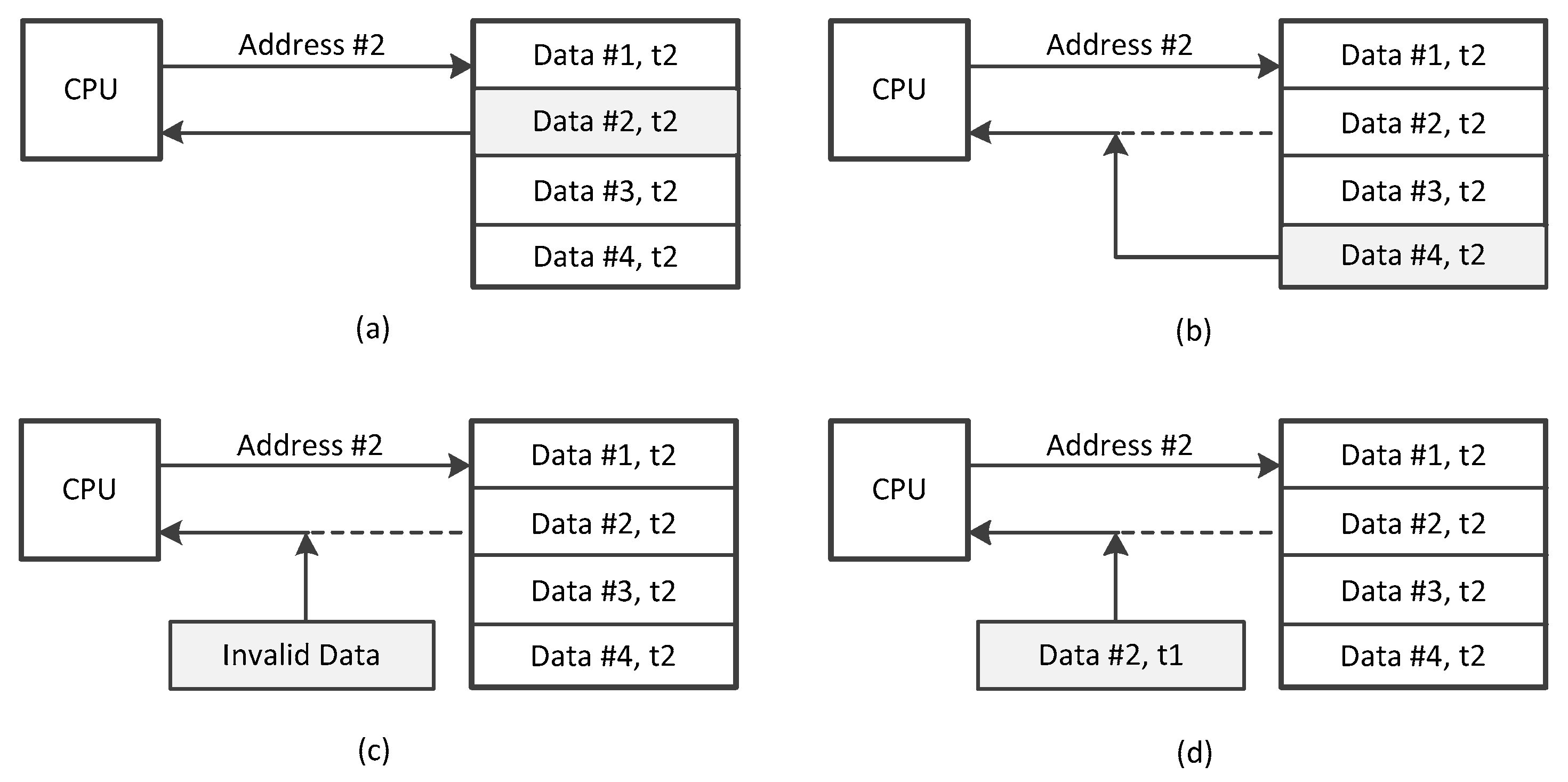
Figure 1 shows the threat model for the data in the embedded systems in the view of the embedded processor. (a) Presents the valid memory access operation to the data stored in memory with address #2 at time t2. The intention of this operation is to load the Data #2 to the CPU. (b) Shows the invalid operation of data splicing attack. The splicing attack involves the attacker intercepting a bus request and returning a valid but non-requested block. (c) Gives the invalid operation of data injection/spoofing attack. The adversaries modify the system data in the external memory with a random value or inject a portion of data. The stack smashing attack uses this method to inject malicious return address into the data section. (d) Demonstrates the operation of data reply attack. Time t1 is reached earlier than time t2. The attacker records the portion of the accessed data. Then, he intercepts a bus request and returns an outdated, potentially stale version of the requested data block. This type of attacks is not easy to be detected by data integrity verification.
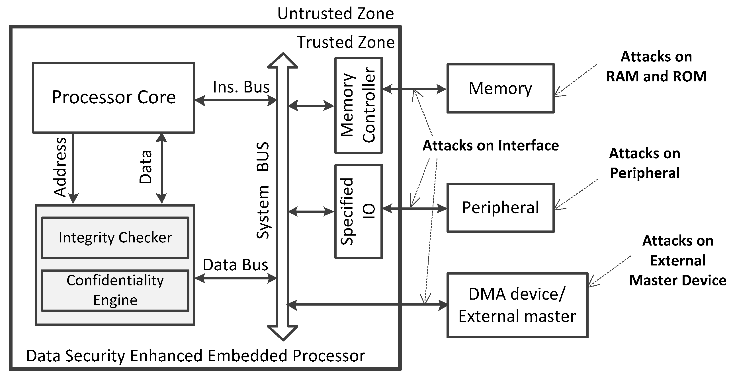
The secure boundary and the potential attacks concerned in this work are shown in
Figure 2. We define the regions on the embedded SoC chip as the trusted zone, while all the interfaces and wires connected to the SoC and all system components and peripherals off the chip are assumed to be untrusted. All adversaries cannot tamper the pipeline, registers, I/D-Cache and any signal inside the embedded processor. This means any program dump is not lead by the crash of the on-chip hardware. All kinds of attacks can be launched at stages ranging from the program installation phase to the loading phase and execution phase. The targets of these attacks include the RAMs and ROMs off the Chip, system components, peripherals, interfaces, and external wires. Some external master devices, such as DMA device, are assumed to be untrusted. The adversaries can exploit the external master devices to access the memory directly.
4. Hardware-Enhanced Runtime Data Protection Architecture
4.1. Overview
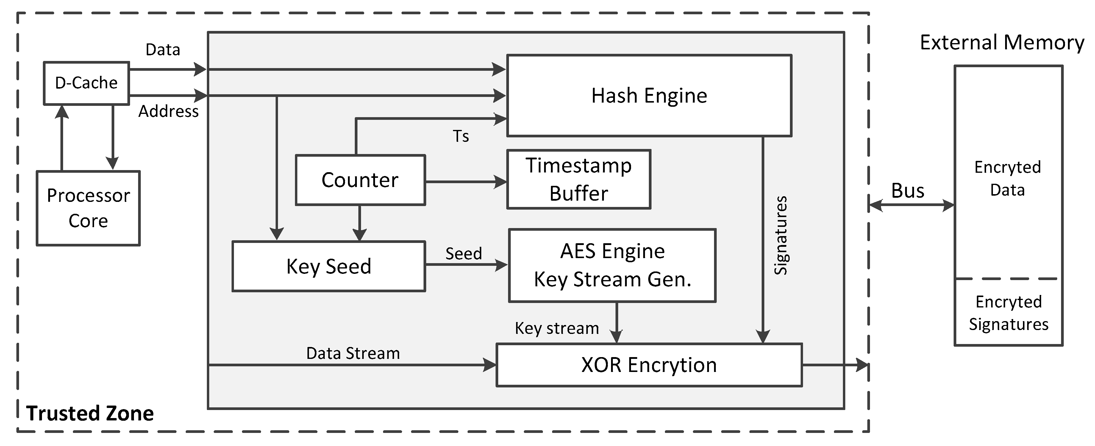
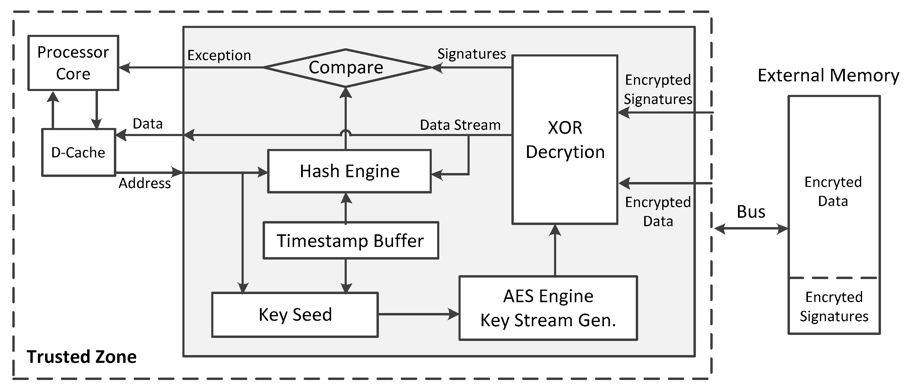
This section gives some details of the proposed hardware-based data protection scheme. The hardware implementation and working mechanism of this work are proposed. In this work, a hardware-based security protection module between the data buffer and external memory is applied, which is in the trusted region. The embedded system with the proposed architecture helps to protect the confidentiality and integrity of the data. The appended location of the security module is outside the data cache, and thus, the module will only be used on the data cache miss occasion. When the data cache status is hit, the processor can access data on the data cache in the trusted region, no additional security mechanisms are required. In the security module, a hardware implemented lightweight hash engine is used to sign and verify the data block transferred between the processor and external memory dynamically. Here we adopt Lhash algorithm, a lightweight hash algorithm suitable for embedded systems, to reduce area footprint and power overhead. To further narrow down the hardware overhead, the hash value of the data will be stored outside the chip together with the dynamic data. This helps to preserve the integrity of the data at runtime. To protect the confidentiality of the data stored off the chip, an AES OTP (One Time Pad) based cryptograph method is used to encrypt and decrypt data and its integrity signature information.
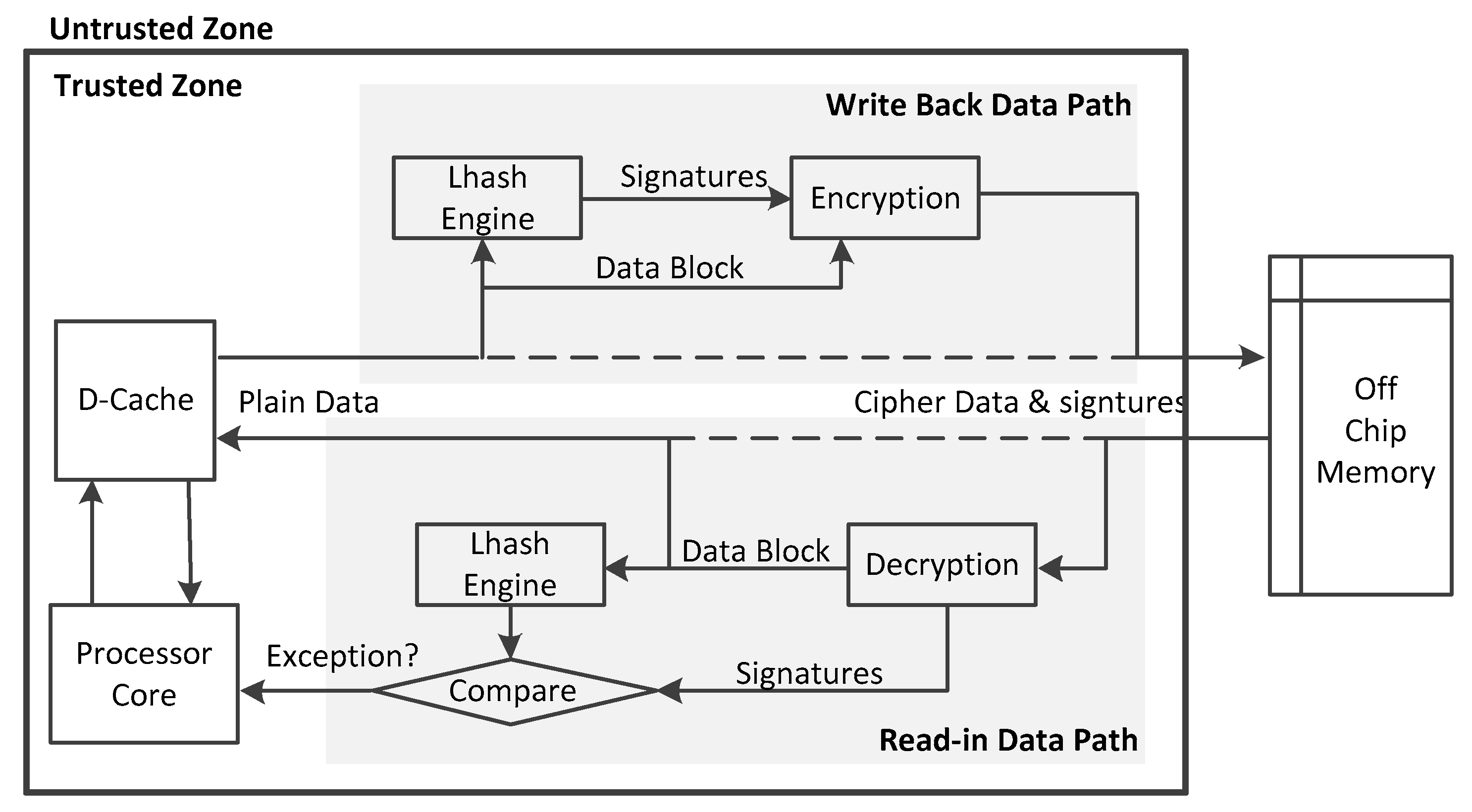
Figure 3 provides the memory access data path of the hardware-enhanced technique that can protect the confidentiality and integrity of data dynamically at runtime. When the on-chip data cache writes back data to an external memory, the hash value of the data block is calculated using the hardware Lhash engine in the security module, as the signature information for the data integrity check. Then, the data block and its signature information are assembled and encrypted using OTP based stream encryption. The encrypted cipher text, including the encrypted data and the encrypted data signatures, will be sent to the external memory. When the processor load data and the data cache assert the miss tag, the data cache reads data block from the external memory, the data block and its signature information will be decrypted first. The hash value of the decrypted data block is calculated again accordingly, as the verification information for data integrity, as compared with the decrypted signatures. The decrypted signatures are computed at data store time. This mechanism can help to find any adversary modification of the off-chip data. When a mismatch is detected, the security module will send an exception signal to the processor, which will trigger the additional response mechanism designed by the user. In the process of program execution, the transmitted data blocks are encrypted or decrypted, and the integrity information of the data blocks is signed or verified at runtime. This provides integrity and confidentiality security of the data stored outside the processor chip with low power consumption and a marginal area footprint.
It is important to note that for the commonly used Harvard micro architecture processor, data write and read operations are not performed simultaneously. When the hardware security module is implemented in the embedded system, only one Lhash engine and OTP based AES encryption engine should be applied. Time division multiplexing of the cryptographic engine is performed at the time of the data read operation and the write operation. This implementation helps to save a lot of on-chip area without incurring much performance penalty. Besides, the AES OTP based encryption scheme uses XOR gates to produce plaintext and cipher text with the key stream generated by AES encryption circuits. Thus, only the AES encryption logic is used in this work, eliminating the hardware overhead induced by the AES decryption circuits.
The data protection granularity is a trade-off between security and system performance overhead. In this security mechanism, on-chip data are signed and encrypted when they are evicted out, and the data are decrypted and verified after they are fetched from external memory and before they are used by the processor. Data transfer between external memory and processor occurs when the data cache misses. Consequently, the most suitable data block size is the cache line size of the lowest level data cache. Multiple caches transmit data in their self-organization in the trusted zone. Generally, we focus on the processor with only one level data cache and code cache for the rest of the paper. We take the cache line size as the size of the data protection unit, which guarantees security while simplifying the process of data protection. Data cache is located in the on-chip trusted area on which cached content is considered as immune to attack. When the data cache conflicts and writes back the data block to the external memory, the data block is attached with a signature that records its integrity information and is encrypted. When the data cache misses and fetches the data block from the external memory, the data block is decrypted, and its integrity is verified.
4.2. Data Integrity Protection
Integrity attack refers to a class of attacks that affect the normal execution of system programs by destroying or tampering with system data and program code. Integrity will be violated whenever any unauthorized code is executed or unauthorized data is used. This section gives the details of the proposed hardware-enhanced data integrity protection method. Some famous integrity protection methods are mainly depending on various authentication algorithms. They are used to generate the checksums of the target code and data at the trusted stage, and these checksums will be verified at a suspicious stage. In this paper, LHash is used to protect the integrity of data, which improves the traditional hash algorithm and makes a tradeoff between security, energy consumption, and implementation cost.
Data integrity is ensured by verifying the integrity signature of the data at run time. Different from the code which can be determined after compiling and linking, the data is highly dynamic and can be modified during the running of the program. For data integrity protection, replay attacks should be considered together with some of the most common attacks that can be encountered, such as spoofing attacks and splicing attacks. To prevent various kinds of data attacks at the same time, the integrity signature is set as the hash value of a collection of inputs, including the actual value of a data block, the starting physical address of the data block, a number that can mark the order of time. The value of the data is necessary to prevent spoofing attacks and partial splicing attacks and replay attacks. Once the value of the data has tampered, the integrity validation information that contains the data content will change. Using the data’s address prevents splicing attacks, since data residing at different addresses will have different signatures, even if the data themselves are identical. To prevent replay attacks on data, a number that can mark the order of time is required to ensure that all fetched dynamic data is up to date. We call the number a timestamp, which is associated with a protected block of data.
The timestamp needs to be generated inside the processor chip and stored in the trusted region. Any circuits and modules off the chip are not allowed to access the timestamp value. We use a hardware counter to generate a value as the timestamp to mark a block access time. When the data cache writes back a data block to an external memory, the count value will be increased. While the counter will be decreased, since the data block is loading to the data cache and processor. Both the counter and timestamp need to be stored in trusted areas, and the timestamp is mapped to the corresponding data block. When the data block is read in, the corresponding timestamp is retrieved in the timestamp memory according to the address. The size of the counter should be treated specially. If the width of the counter register is not enough, the count value will overflow quickly, and the time uniqueness of the key seed cannot be guaranteed. However, if the width is set too large, the storage of the count value will take up much on-chip storage. Thus, the size of the counter should be selected according to the application requirements, and there is a balance between the security and the storage overhead.
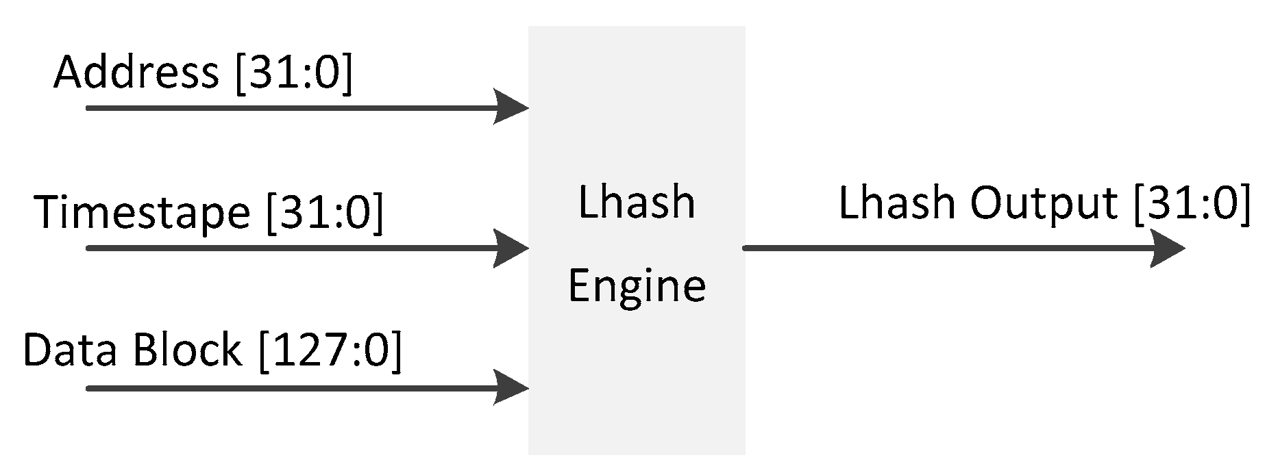
The implementation of the data integrity protection architecture adopts Lhash as the lightweight hash algorithm, which is used to sign and verify the data block stored in external memory. The hash algorithm is a kind of unidirectional compression algorithm, whose mechanism is to compress the information of any length into a fixed length output through a certain compression structure. We take a 32-bit scalar RISC processor with a Harvard micro architecture as an example to illustrate the process of signature generation. The cache line size is set as 128 bits. Thus, the granularity of the protection data block is 128 bits. Additionally, a 128 bits timestamp and 32 bits signatures are used in this work. The inputs and output of the Lhash Engine are shown in
Figure 4.
For the hardware LHash computing circuits, we set the 32 bits instruction as the message block XORed to part of previous permutation state and enter into the next permutation engine in the extended sponge function. The optional block size of the LHash internal permutation is 96 bits and 128 bits in this situation. The security properties of the LHash algorithm based on the sponge construction can be concluded as Equation (1) [
27].
where
n is the digest size,
c represents the capacity size of the internal permutation, and
r represents the length of the input message blocks. In this work, the absorbing size
r is fixed to 32 for the 32 bits RISC processor data. In tag-based applications, 64 or 80 bits security is often appropriate instead of complex constructions providing high security primitives, such as a 512 bits output hash function [
28]. In our case, we require at least 64 bits pre-image resistance security, and 48 bits collision and 2nd pre-image resistance security. Thus we choose the permutation F128 with the parameter that
r = 32,
c = 96, and
n = 96. The Lhash with these parameters can provide 64 bits pre-image security, 48 bits 2nd pre-image security and 48 bits collision security. During the execution of the program, the address, timestamp, and data block will be sent to the input of the Lhash engine sequentially.
The signature is generated before the data is written to the external memory when it leaves the on-chip trusted zone. When the data is read into the chip, it is necessary to recalculate its integrity information and compare it with the previous signatures. If the two signatures are inconsistent, the integrity of the data is frustrated. Therefore, signatures need to be protected as a reference to determine whether the data is subject to integrity attacks. They could be stored in the trusted area on the chip to avoid attacks, but this will lead to large on-chip storage overhead. In order to avoid the use of expensive on-chip memory, we encrypt the signatures and save them to the external memory, and establish the address mapping relationship with the corresponding data block. The signature is transmitted on the data bus after its corresponding data block and is encrypted and decrypted following the data block.
4.3. Data Confidentiality Protection
Confidential attacks aiming at stealing confidential and sensitive information from the system are not a new threat to the embedded systems. Besides, the attacks such as code injection, data modification, and some new ROP/JOP based advanced attacks can be performed by obtaining and analyzing the data and code stored outside the trusted regions. The code and data concealing technology can defend against various kinds of attacks effectively. To protect the confidentiality of embedded systems, it is necessary to ensure that the data out of the processor chip are encrypted and cannot be cracked easily. The protection of data confidentiality is usually realized by encrypting the data in the untrusted area, which makes the data monitored or stolen by the attacker as an incomprehensible random code, preventing the disclosure of the confidential information. In this paper, we adopt AES (Advanced Encryption Standard), which has the advantages of good security and easy hardware implementation.
The embedded systems have limited on-chip resources and processor performance, and cannot use excessive pipeline performance to handle encryption and decryption operations. Therefore, a hardware AES should be designed to encrypt and decrypt the off-chip data. The junction location of the encryption and decryption engine in the embedded chip must be handled carefully to reduce the impact on the processor performance. There are two ways to encrypt system data by using AES. One is the block encryption method [
29], in which the content of the data block is used as the input of the encryption algorithm and the output is the cipher of the data block. The other is OTP based stream encryption, that is, the AES algorithm is used as a key stream generator to generate a series of random numbers, and the data can be encrypted and decrypted by performing the XOR operation with the sequence.
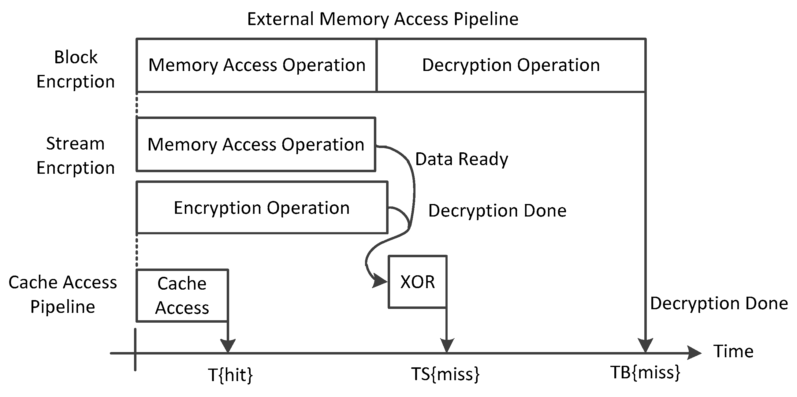
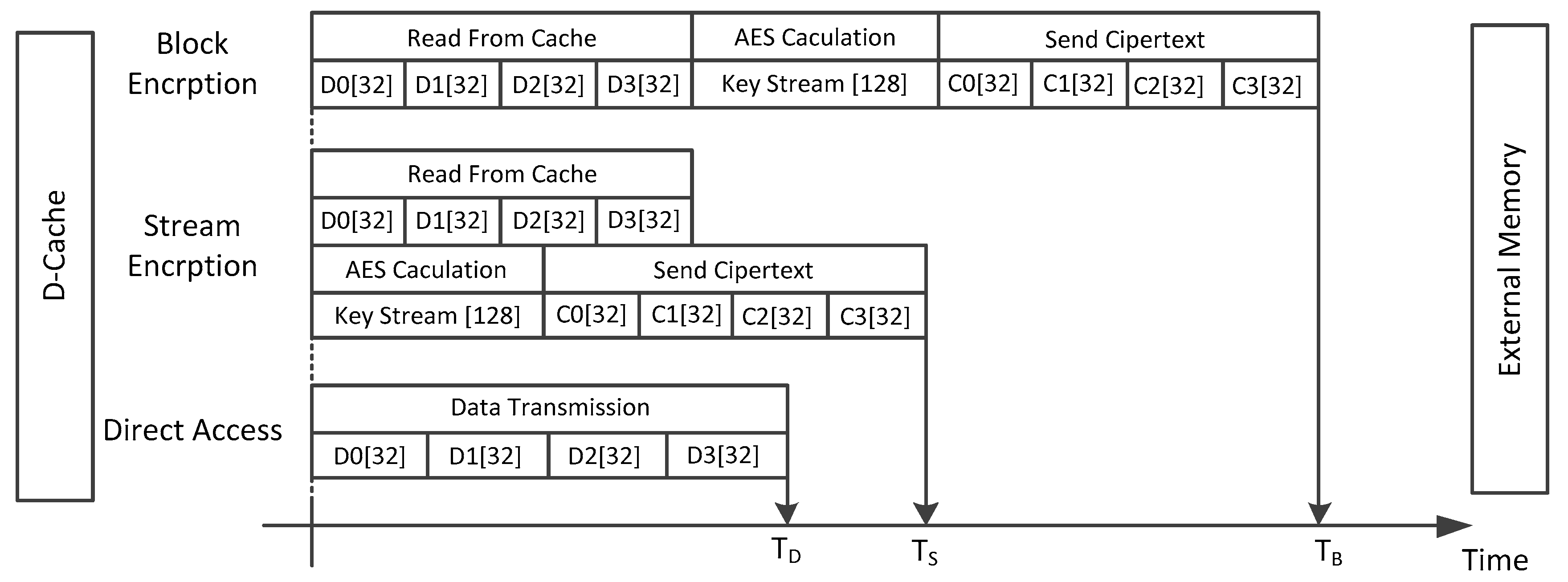
The processor memory access time diagram of a write-back operation from the data cache for these two methods is shown in
Figure 5. In this figure, the write-back operation interval times for direct access without cryptographic security, OTP based stream encryption and block encryption are marked as a contrast. In the embedded system with a 32 bits RISC embedded processor mentioned in the last section, the data bus is 32 bits, and the data block is 128 bits. Block encryption requires the acquisition of a complete block of data before encryption and decryption. To complete the data block transmission on the bus, the data bus needs access the data cache four times to get a data block. Then, the AES encryption engine works to calculate the cipher before send to the external memory. The stream encryption process is parallel to the data stream transmission process. The security module with stream encryption mechanism calculates the key stream before transmitting the data block. Then, during the transmission of the data block, the data stream is encrypted by performing an XOR operation with the key stream. Compared with the two methods, the stream encryption method has less security delay.
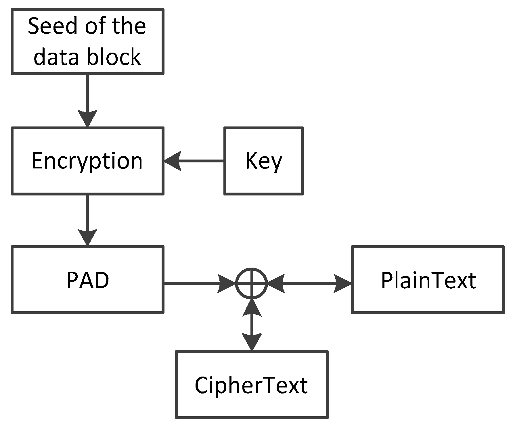
It is significant for the key stream to be random and unique. If the key stream has a high repetition rate, this is vulnerable even with the mechanism of encryption. It may potentially permit an attacker that doesn’t take much effort to guess the key stream. Besides, we have to make sure that the data at different locations in the external memory has different seeds. For this reason, we use the physical address of the data block as part of the seed to ensure the spatial uniqueness of the key stream. In addition, for a specific address, the data written each time is required to correspond to a different seed. Therefore, we require that the seed contain time information to ensure the time uniqueness of the key stream. We use the counter and timestamp mentioned in the integrity protection as a part of the seeds. The procedure of the OTP stream encryption and decryption is shown in
Figure 6.
The seed of the data block is assembled by the address and timestamp of the target memory block. These contents are only related to the address and access time of the target memory space, instead of the data transferred. Therefore, with the process of encryption and the seed by the AES engine, the memory access process can be performed in parallel. This reduces the system performance loss caused by the confidentiality protection mechanism. The OTP based encryption method is used, and the pad is generated by the encryption of the seed. Thus, the encryption process of the data can be written as
The decryption process of the data can be written as
where
C is the cipher,
P is the plaintext data value, and
AESKEY(
seed) is the key stream having the same bit width with
P. This implementation structure can save more performance loss at a load operation. It can be inferred from
Figure 7. When the processor tries to load data in case of data cache miss, the physical address of the target data will be asserted at first. Then, the memory controller is authorized to load the encrypted data from external memory. The seed for the AES engine is fixed at the same time. Thus, the AES engine to calculate the pad and the memory access operation can be synchronized. After the two operations are completed, only one delay of the XOR operation is required, and the external data can finish the load and decryption.
It can be seen from
Figure 7 that the external memory load operation uses a hardware AES encryption engine to finish the data decryption, instead of a hardware decryption engine. Therefore, in the process of hardware confidentiality protection, only one encrypted AES engine can be used to complete the encryption and decryption operations of the data, without requiring hardware implementation of a decryption AES engine. This helps to decrease the costly hardware overhead to a large extent.
In order to further reduce the consumption of the hardware resources, we implement AES encryption engine with composite field arithmetic. AES process 8-bit state in finite field arithmetic on
GF(2
8) elements. The most common approach for the four steps is using lookup tables initialed by the aimed results. This may cause a lot of waste in hardware resources due to the storage units have a large area. In the mathematical theory, the finite field of
GF(2
8) can be built iteratively from
GF(2
4) using irreducible polynomials
where
x is an element in
GF(2),
y and
β are elements in
GF(2
4). In this work, we implement AES using
β = {1100}
2. The byte substitution transformation in the encryption process can be divided into two steps, the modular inversion and affine transition over
GF(2
8). In the modular inversion stage, the state in
GF(2
8) is first mapped in
GF(2
4) using an isomorphic mapping matrix T. Then, the inversion in
GF(2
8) is reduced to be inversion operation in
GF(2
4). After the reduced inversion operation, an inverse isomorphic mapping is performed. At last, an affine transition matrix is used in the affine linear function. The modular inversion operation in
GF(2
8) is decomposed as three steps linear operation and one step reduced modular inversion. The byte substation module is the most frequently used module in AES. In a round pipelined encryption implantation, there needs 20 byte substation modules, 16 for the byte substation stage, and four for the mix column stage. The mix column transformation, shift row transformation, and round key addition involve some multiple and XOR computation in
GF(2
8), this is easy to implement in hardware as this operation can be mapped to gate elements and straight wires in circuits.
4.4. Memory Accesss Procedures with the Hardware Enhanced Security Mechanism
In this section, we will describe the memory access procedures with the hardware enhanced security mechanism. The memory access procedures have a close relationship with the data bus width and the data protecting granularity. We take the embedded system with OR1200, one fully open source OpenRISC 1000 architecture processor, as an example in the illustration. OR1200 is a Harvard RISC processor with 32 bits instruction and data bus, and the cache line size is set as 16 bytes. The working process of the security module for protecting data can be divided into two parts, the data from the data cache writing back to the external memory, and the data from the external memory loading into the on-chip cache. Procedure 1 describes the working process of the write-back procedure, and the hardware details of this procedure are shown in
Figure 8.
| Procedure 1: Data write-back operation with hardware enhanced security |
| inputs: address, DATA |
| outputs: ts, CIPHER_D, cipher_s |
| DATA ← set of datai in current data block to write back, 0 ≤ i ≤ 3 |
| CIPHER_D ← set of the encrypted data cipher_di, 0 ≤ i ≤ 3 |
| 1: assert the target address, map address to physical address |
| 2: ++ts |
| 3: generate seed = {physical_address, ts} |
| 4: key_stream = AESkey (seed) |
| 5: for all datai DATA do |
| 6: cipher_di = key_stream [i+31: i] ^ datai |
| 7: write cipher_di out |
| 8: Lhash_value = fLHash(Lhash_value, datai) |
| 9: cipher_s = key_stream ^ Lhash_value |
| 10: write cipher_s out |
When the data cache conflicts and prepares to write back the data block to the external memory, the appended security module acquires the data block address from the cache and waits to receive the data block from the cache. Then the timestamp is generated by increasing the counter by one. The count values are stored in the trusted timestamp buffer on the chip and mapped to the physical address of the data block. At the same time, the seed to be encrypted by AES engine is assembled, since signal conjunction can be mapped to gate elements and straight wires in circuits easily. Then, a 128 bits output is obtained by hardware AES encryption engine, in which there is a uniqueness of time and space to a large extent. The sequence can be used as a key stream to encrypt the data stream. Then the hardware security module reads data from the cache line, operates XOR with the corresponding bits in the key stream, and sends to the target external memory. Since the inputs of the hash engine are prepared, the Lhash calculation works simultaneously. To reduce the overhead of on-chip storage, the signature is encrypted and stored off the chip as well. Similarly, Procedure 2 presents the working process of the load procedure, and the hardware details of the load process are shown in
Figure 9.
| Procedure 2: Data load operation with hardware enhanced security |
| inputs: address, ts, CIPHER_D, cipher_s |
| outputs: DATA, exception |
| CIPHER_D ← set of the encrypted data cipher_di, 0 ≤ i ≤ 3 |
| DATA ← set of datai in current data block to write back, 0 ≤ i ≤ 3 |
| 1: assert the target address, map address to physical address |
| 2: ts-- |
| 3: generate seed = {physical_address, ts} |
| 4: key_stream = AESkey (seed) |
| 5: load CIPHER_D, cipher_s |
| 6: for all cipher_di CIPHER_D do |
| 7: datai = key_stream [i+31: i] ^ cipher_di |
| 8: write datai to D-cache |
| 9: Lhash_value = fLHash(Lhash_value, datai) |
| 10: Lhash_value_pre = key_stream ^ cipher_s |
| 11: if Lhash_value_pre = Lhash_value then |
| 12: exception = NULL /* integrity valid */ |
| 13: else exception = assertion /* integrity invalid */ |
In the case of a data load operation from the external memory, the physical address is first asserted and sends to the security preserving hardware and the external memory. Then, the safety protection hardware and external memory work, respectively. The security module pops the buffered timestamp and generates the key stream as described in the write-back procedure. At the same time, the read operation to the external memory feeds back the encrypted data and corresponding encrypted signatures. The encrypted information can be decrypted using the 128 bits key stream. Then the hardware Hash engine calculates the hash value with the decrypted data rapidly. At last, the decrypted signature will compare with the calculated signature, and the exception signals will be sent to the processor if any violation is detected. The parallel of the security mechanism and the memory access operation helps to save performance overhead, respectively.
5. Experiment and Discussion
5.1. Experiment Setup
In order to assess the performance and implement overhead of the proposed hardware-enhanced protection method for the runtime data security, we build the embedded system based on the OR1200 processor, which is a 32-bit scalar RISC processor with a Harvard micro architecture. The size of the instruction cache and data cache can be configured as 1 KB, 2 KB, 4 KB and 8 KB respectively. In this work, we set OR1200 soft core with 4 KB Instruction Cache and 4 KB Data Cache as a typical configuration. The frequency of the core is @100 MHZ in this experiment, fully synchronized with the security module designed. Different types of the external memory may have different access efficiency, and we thus employ both SSRAM and SDRAM in this work. The controllers of the external memory are implemented on chip, and the storage chips are extra chips on the board. Then, the SoC with the proposed architecture is implemented on the Xilinx Virtex 5 FPGA platform. After the compilation and mapping, the design is projected to FPGA slices.
Table 1 shows the FPGA resources used for the experimental embedded system.
5.2. Hardware Implementation Overhead
Security protection schemes are generally implemented by cryptographic calculation. Embedded systems have limited system resources and it is insufficient to allocate excess system performance for the software based cryptographic operations. Therefore, the hardware based protection method is a good choice. However, the appended modules inevitably increase the hardware implement overhead, which may lift the chip area and power consumption. The proposed runtime data protection scheme uses hardware based cryptographic method to protect the integrity and confidentiality of the data stored off the processor chip, this increases the implementation cost of the embedded system. There must be a trade-off between the security, performance, and the hardware cost. The hardware implementation overhead must be considered in advance.
In this work, we adopt Lhash to perform data integrity verification, and AES to achieve data confidentiality protection. The resource consumption has been considered during the design phase, together with the protection architecture. For the integrity protection, we use the lightweight hash function Lhash, which maps the digest sizes of 80, 96, and 128 bits. We minimize the length of the internal permutation and design an F96 structure to perform internal absorbing and squeezing on the basis of satisfying the security requirement of the Lhash algorithm. The hardware implementation of the Lhash engine with F96 internal permutation structures needs only 871 gate elements (GE). The hardware implementation of SPONGENT [
27] with 136 bits internal permutation and PHOTON [
28] with 144 bits internal permutation cost 1103 and 1394 GE, respectively. In this work, the implementation overhead is much less than the lightweight hash function SPONGENT and PHOTON, while providing the close security bounds. In addition, the signatures storage overhead is about 25% of the data storage capacity. It is unacceptable to store the golden hash value on the chip as presented by Xiang Wang [
9]. Therefore, we store the encrypted signature in the external memory, which saves the hardware overhead for a lot. For the confidentiality protection, the OTP based stream encryption method does not need the implementation of the AES decryption circuits other than the AES encryption engine. On the design of the AES encryption engine, we replace the lookup table based substitution boxes with the ones with composite field arithmetic. According to some of our previous work on the FPGA chip, the AES engine implemented with composite field arithmetic can save 53.24% logic cells, as compared to the implementation with the lookup table.
The timestamp is used in both the integrity and confidentiality protection to ensure the time uniqueness of seeds. The max size of the counter that generates timestamps needs some special consideration. If the counter is designed small, the count value may overflow quickly resulting in a high repetition rate of timestamp, and the time uniqueness of the key seed cannot be guaranteed. This may reduce the security of external data. However, if the counter is set with much redundancy and the timestamps may waste too much on-chip storage space. Therefore, the size of the counter should be selected according to the application requirements, and there is a balance between security and storage overhead. In this work, an 8 bits counter is used in our experimental platform. Each 128 bits data block of the system is attached with an 8 bits timestamp, with about 6.25% on-chip storage overhead of the data memory space. The FPGA resource overhead of the proposed hardware mechanism, the security enhanced processor and the SoC is shown in
Table 1. The proposed security module occupies less than 32.1% registers and 40.2% LUTs of the overall SoC. The OR1200 is a relatively smaller processor. For the embedded system with processors much bigger than OR1200 in the area, such as ARM, MIPS, SPARC, and RISC-V, the proposed security module may have less impact on the system area and power consumption.
The main hardware overhead of the proposed mechanism is the storage for the buffered on-chip timestamp and the external signatures. The size of the internal and external extra storage overhead is dependent on the size of the target data space. In this work, each 128 bits data block with 32 bits external signature attaches an eight bits on-chip timestamp, with 5% on-chip storage overhead and 20% external storage overhead of the target data memory space. Thus, the 128 KB target data space has 6.4 KB on-chip storage overhead and 25.6 KB external storage overhead. Rogers [
25] proposed a security extension method for the data confidentiality and integrity in embedded systems, using a hardware dynamic sequence number table and a page root signature table. They implemented their work in Sim-Panalyzer ARM Simulator, and the 128 KB target data space needs 42.7 KB storage to store the signatures. SecureME [
30] is implemented on Simics emulator. The hardware overhead for the data security includes a 32 KB on-chip RAM and 1.6% external memory space of the target data space. For the same 128 KB application, the storage overhead for SecureMe will be 34 KB. Compared with these two works, our approach is implemented in real hardware and has less hardware overhead.
5.3. Performance Overhead
The security mechanism inevitably causes a loss of system performance. To reduce the performance overhead of the data encryption and signature verification, some efforts have been made in the proposed architecture. In this mechanism, the hardware-enhanced security scheme attaches the security module between the data cache and the external memory, and the data blocks transmitted between them are used as data protection units. Therefore, the data encryption and signature generation processes are only performed on the data cache write back occasions, while the decryption and signature verification processes are performed on the data cache load situations. The data cache in the embedded processor has a high hit rate, so the hardware structure we proposed has less impact on the system performance.
The external memory latency is higher compared with the speed of the processor. The mechanism providing runtime data confidentiality and integrity is designed with little latency by performing the cryptographic operations in parallel with the memory access processes. In the confidentiality protection process, the input vectors of the AES encryption engine are the target address and corresponding timestamp, which have been asserted since the processor required the external data. Therefore, the simultaneous work of the AES encryption engine and the memory access process helps to hide the AES encryption latency. After the generation of the key stream, the plain text and the cipher can translate through a simple XOR operation. In the data integrity protection process, the Lhash engine is not appended on the data path, except for the signature store and load stage. The data block can still transfer between the data cache and the external memory, while the hash value of the data block has not been calculated yet. Thus, the performance impact of the time-consuming Lhash calculation is decreased.
In our experiment, we select various scales of benchmarks from Mibench suite [
31] to generate realistic workloads. All of these benchmarks are compiled by the GNU Cross Toolchain or32-elf-gcc, and are executed on the FPGA board. A 2MB SSRAM IS61LS51236A is used as the external memory of the runtime data, which provides a faster memory access speed than other types of memories. This may magnify the performance overhead. In our work, it is obvious that the hit rate of the data cache may influence the performance overhead of the proposed scheme. For the purposes to record the data cache hit rate, we use or1ksim [
32] as the system simulator. At first, we configure the processor with 1KB data cache.
Table 2 gives the cache hit rate, CPI (Clock cycle Per Instruction, without security mechanism), CPI secure (CPI, with the proposed security mechanism), and the performance overhead of the selected benchmarks.
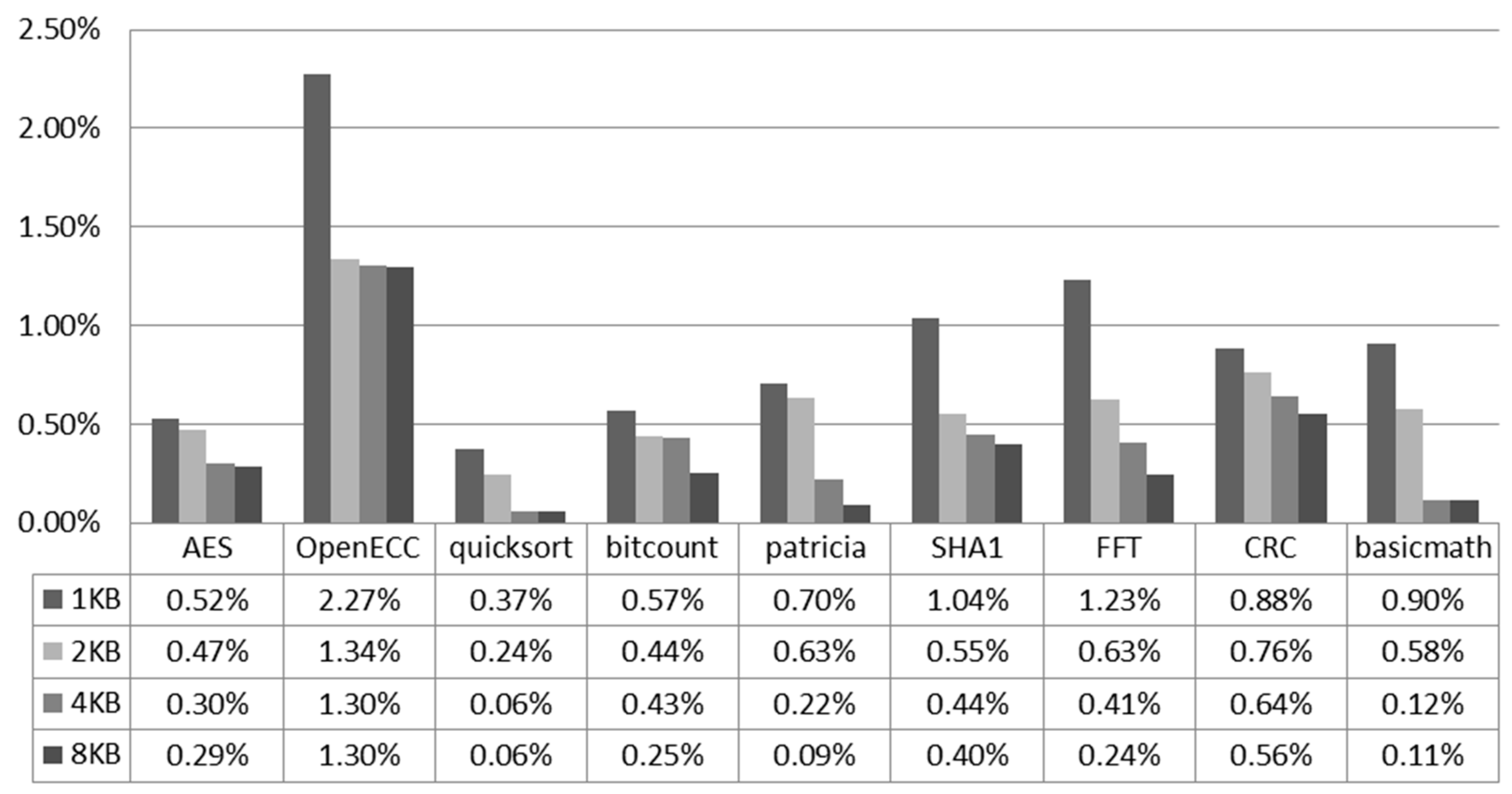
The average performance overhead across the selected benchmarks is 0.94%, ranging from 0.37% (quicksort) to 2.27% (OpenECC). In embedded systems, the main performance overhead is caused by the response of the external device. The memory access response accounts for the vast majority. The CPI can reflect the proportion of the memory access instruction in the binary code. The more memory access instructions in a benchmark, the higher the CPI will be. For the benchmarks such as AES, OpenECC, Sha1, FFT, and basicmath, which require a large number of memory access operations to store temporary data, the CPIs are higher than other benchmarks. In most of the benchmarks, the higher CPI means the higher performance overhead of the proposed security mechanism. This is because once the data cache misses, the append security preserving hardware may incur additional clock cycles. The AES benchmark is an exception, because of the higher data cache write and load hit rate. The processor can increase the size of the cache to reduce the miss rate. This can help the proposed work to decrease the performance overhead.
Figure 10 shows the performance overhead of the selected benchmarks with 4 KB instruction cache and 1/2/4/8 KB data cache. In the embedded system configured with 8 KB processor data cache, the performance overhead of this work ranges from 0.06% to 1.30%. The proposed design has a small impact on the performance of the embedded system.
5.4. Security Analysis
We design the experimental SoC with JTAG TAP and Advanced Debug Interface (ADI) [
33] to provide memory access bypassing the processor data path. The ADI is connected to the master interface of the wishbone bus. During the execution of the program, the JTAG device can break the execution, and modify or check the data values stored in the external memories. The external data status helps us to evaluate the security protection features.
In the data transfer process between the embedded processor and the external memory, the data is encrypted before sending off the chip and decrypted after receiving from the external device. The data off the chip is in form of cipher text. It is obvious that the hardware-enhanced processor with the proposed architecture can provide data confidentiality in the embedded system. The hardware AES encryption engine is used to generate the key stream. Then the plain data and the cipher data can translate through a simple XOR operation with the key stream at runtime. The hardware based data encryption and decryption operations are all assembled in the proposed security module in the trusted zone. Only the target physical address, the encrypted data, and encrypted signatures can be fetched by the external adversaries. Nevertheless, the robustness of the key stream affects the ability against the deciphering or decrypting attacks. The hardware timestamp is generated, buffered, and used in the security-enhanced processor, which will not be sent out of the trusted area. Even if the target address is intercepted by the adversaries, it is impossible to acquire the value of the key seed. Some further deciphering or decrypting attacks become difficult to conduct. This enhances the robustness of the proposed confidentiality protection method. Thus, any adversary actions including the bus snooping attack aiming at stealing the critical user information and program data will be disabled. The board level side channel attacks analyzing the board signals cannot get the actual data easily to perform detrimental attacks. Some advanced attacks for the embedded systems try to link valid program gadgets to conduct ROP and JOP attacks. The encrypted stack and the hidden return data in the memory make these attacks difficult to follow.
In terms of the integrity protection, the signature is calculated in the security module before the data off the chip, and the integrity signature of the data block is recalculated and compared with the decrypted signature at load time. This process requires the consistency of the signature, that is, the data block load from the external memory must be the same with the write one. The spoofing attack tampering with a piece of data in the external memory can be detected, because the changes of the data block content will destroy the insistence of the golden signature. Similarly, the splicing attack and replay attack can also cause mismatches in the signature, since the address details and timestamp are changed, respectively. Besides, in order to reduce the on-chip storage overhead, the signatures are encrypted and stored in the external memory. The confidentiality protection of the signature makes the collision attacks to the data integrity protection mechanism harder to implement.
6. Conclusions
This paper presents a hardware-enhanced protection scheme for the runtime data security in embedded systems. The proposed architecture uses hardware implemented lightweight hash function and AES stream encryption engine to protect the runtime data integrity and confidentiality. For the integrity protection, the signature is calculated by the hardware Lhash engine before the data off the chip, and the integrity signature of the data block is recalculated and compared with the decrypted signature at load time. The inputs of the hash engine include the data block, data address, and the timestamp, which provide the security to detect the data spoofing, splicing and replay attacks, respectively. For the confidentiality protection, the OTP based AES stream encryption method is used. The AES encryption engine can work simultaneously with the memory access operation, without a requirement of the hardware implemented decryption logic. Some details are considered in the hardware implementation of the security module to reduce the hardware overhead and performance overhead.
To evaluate the overhead of the proposed scheme, we implement a SoC with the presented architecture in Xilinx Virtex 5 FPGA platform as a prototype system. We use various scales of benchmarks from the MiBench suite to generate realistic workloads for the processor. The result shows that the proposed hardware-enhanced protection scheme can detect data spoofing, splicing and replay attacks, and provide data confidentiality for the external memories. The performance overhead ranges from 0.37% to 2.27% for the 1 KB data cache, and from 0.06% to 1.30% for the 8 KB data cache, according to the selected benchmarks. Besides, the prototype system has advantages of low power consumption and marginal area footprint.


