1. Introduction
Comparators are omnipresent building blocks in mixed-signal systems. Applications such as memories [
1,
2,
3], data receivers [
4,
5,
6], and Analog-to-Digital Converters (ADCs) [
7,
8,
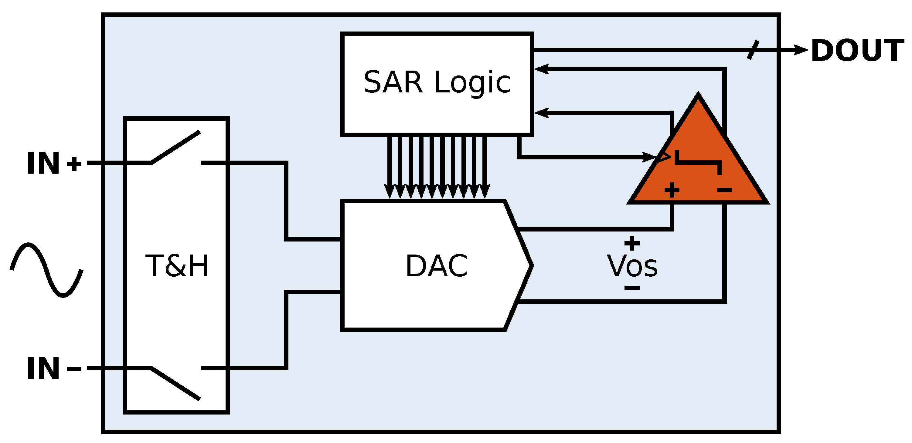
9] necessitate high speed, low noise/offset, yet power- and area-efficient designs. Their role in ADCs (Successive Approximation Register (SAR), flash, pipeline) (
Figure 1) is of special importance, since they need to accurately translate small analog signals into digital information. Therefore, their noise, offset, and speed dictate the overall ADC performance.
Dynamic latch-type comparators [
10,
11,
12,
13,
14] have become very attractive due to their fast regeneration time, enabled by strong positive feedback, and their zero static current consumption. Owing to their highly digital nature, these comparators are able to scale excellently into deep-submicron nodes. To maximize speed for minimal power, small transistor sizes with minimum parasitic loading on the critical nodes are preferred, but they come at the cost of a significantly increased offset [
15,
16].
One straightforward approach is to add amplification stages prior to the latch to suppress the offset voltage referred at the input [
17]. This comes at the expense of increased power consumption due to the high gain and wide bandwidth requirements of these amplifiers. Alternatively, offset compensation schemes have been presented, in the form of adding digitally-controllable capacitors at the comparator outputs [
18,
19,
20]. Further, several charge-pump implementations with extra logic and biasing voltages [
21,
22,
23] have been proposed. However, all these approaches degrade the comparator and its calibration loop speed, increase design complexity and area, and limit robustness.
In this work, a dynamic self-calibration loop is proposed, able to reduce the comparator input-referred offset by a factor of ten. Its accuracy is limited only by the comparator noise, while its short critical path ensures no speed degradation. Finally, its compact size barely loads the comparator output. The loop’s dual-sided implementation greatly enhances the calibration range, while its highly digital nature makes it readily scalable into deep-submicron nodes. Combined with a multi-stage, high-speed, low-noise dynamic comparator, >10 GHz operation is demonstrated with <1 mV input-referred noise (10 b accuracy), rendering it a perfect candidate for multi-GHz, high-resolution ADCs.
This paper is organized as follows.
Section 2 describes the concept of the proposed dynamic comparator calibration.
Section 3 discusses the circuit level implementation of the calibration and the comparator topology, supported by simulation data.
Section 4 summarizes the measurement results along with a state-of-the-art comparison. Finally,
Section 5 draws the conclusions of this work.
2. Dynamic Offset Calibration
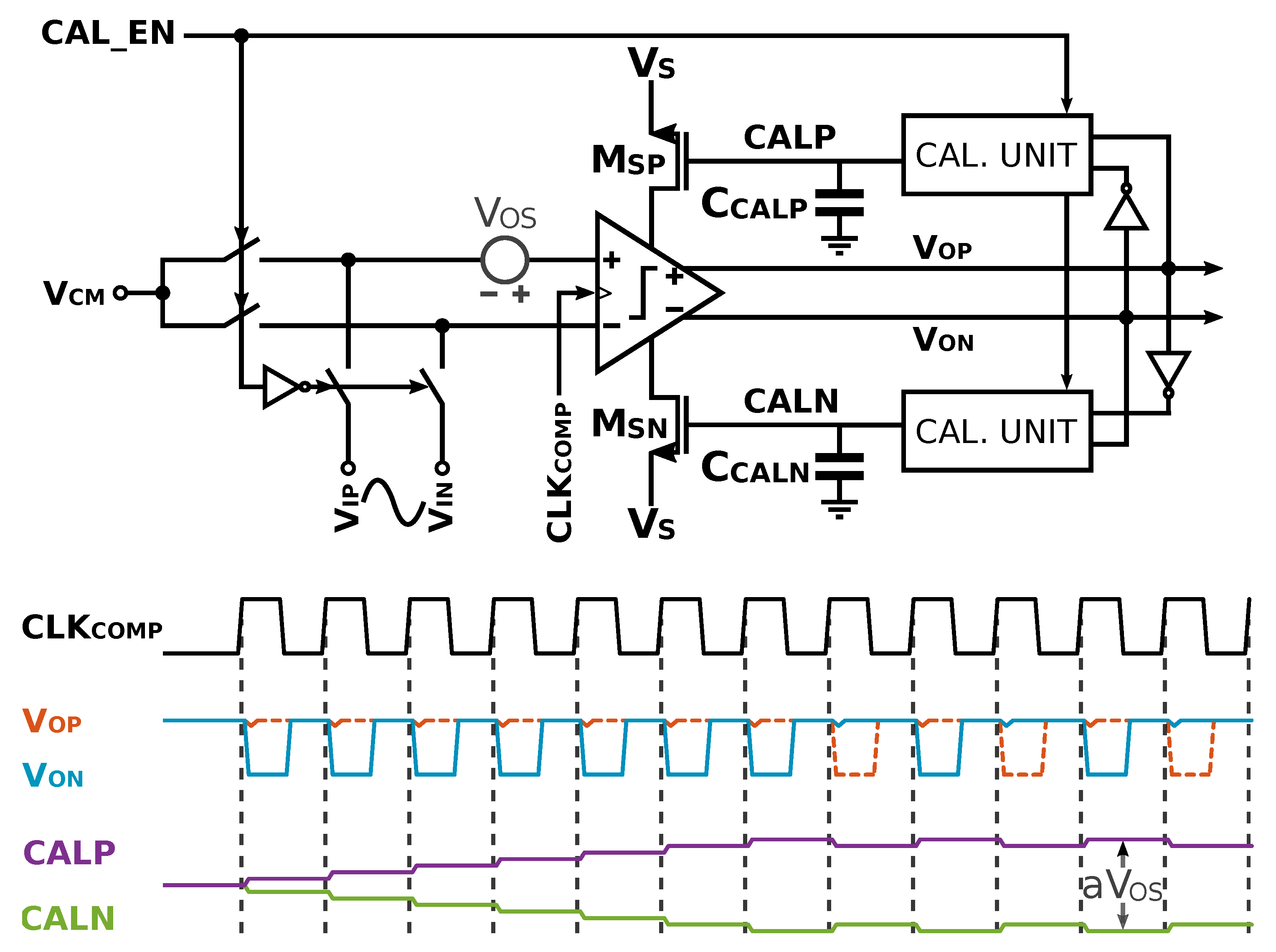
The top-level architecture of the proposed offset calibration principle and its timing diagram are illustrated in
Figure 2. The loop comprises a clocked comparator, two switched-capacitor calibration units (one for each side), and two offset compensating devices
-
. The calibration is performed simultaneously on both sides of the comparator (dual-sided), which maximizes the calibration range.
During calibration mode (CAL_EN is high), the common-mode voltage
is applied to both comparator inputs. For a positive offset voltage
, the differential comparator output will be positive. The output sign is sensed by the two calibration units, which start subtracting charge from
and adding charge to
, forcing nodes CALP/CALN to move in opposite directions to cancel this offset. When their difference reaches a certain value a
, with a >1 depending on the size ratio of
/
and the input transistors (see
Section 3.2), the comparator differential output changes sign alternately. This means that the offset has been compensated, and the comparator now sees an input difference dictated only by noise. During conversion mode (CAL_EN is low),
/
store the offset value, allowing the comparator to operate with canceled offset and decide correctly down to the noise level.
The comparator with the proposed calibration circuit can be easily incorporated in an ADC, where the already available periodic sampling clock can be used as CAL_EN, avoiding extra circuitry to generate that signal. Upon starting up the ADC, the calibration gradually corrects the comparator offset in multiple sampling cycles, by moving small packets of charge in each cycle until the required CALP/CALN difference is reached. This allows the offset calibration to run continuously in the background, tracking supply noise, which can affect the input-referred offset, offering a true dynamic cancellation, while not interfering with the ADC operation.
3. Circuit Realization
3.1. Dynamic Self-Calibrating Loop
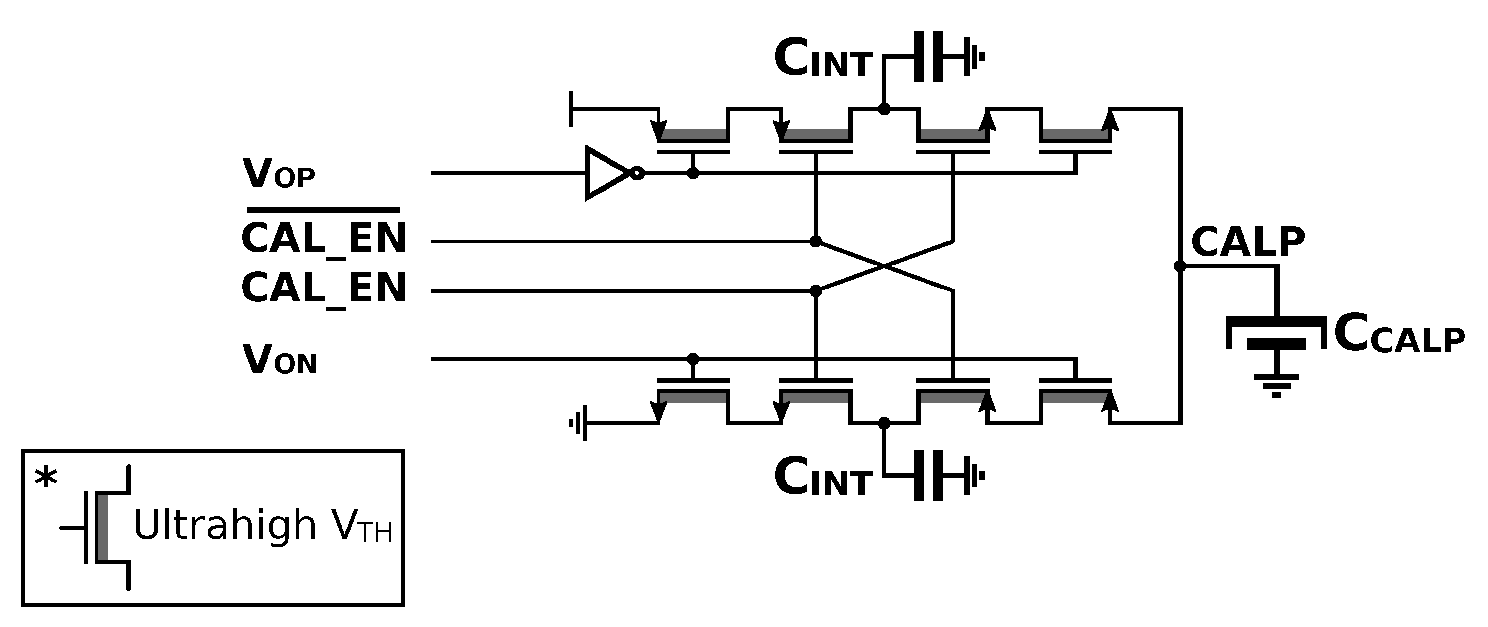
The single-ended version transistor-level implementation of the fully-differential self-calibration unit is shown in
Figure 3. The unit consists of only eight switches plus one inverter. To eliminate the loading at the comparator output, all devices are minimum sized, while the fully-dynamic structure minimizes power overhead. Further, the delay between the comparator output and CALP/CALN is kept to a minimum of two transistors, such that the calibration loop does not impose a limitation on the total comparator speed. Unlike [
21,
22,
23], there is no need for extra biasing circuitry to set the common-mode voltage on CALP/CALN. Here, it is gradually approaching the value set by proper sizing of the switches’ on-resistance.
Charge is re-distributed between one of the internal capacitors and and the amount of charge moved (calibration step) is controlled by the ratio of these capacitors and the time the calibration loop has available in each cycle, resulting in a wide compensation range. To reduce leakage on , this capacitor has been constructed strictly as a Metal-Oxide-Metal (MOM) capacitor. Furthermore, ultrahigh transistors are employed at the expense of more cycles required to compensate a certain offset value. In this way, the calibration step in each cycle is traded-off with the number of cycles. This is never a problem when testing an ADC, since there is always an allocated start-up time, after which useful data are collected and processed. The ultimate accuracy limitation of the proposed calibration technique is the comparator sensitivity to various conditions ( and/or ). Therefore, a high-speed, low-noise, and low-input sensitivity comparator is needed to yield optimal results.
3.2. Comparator Core
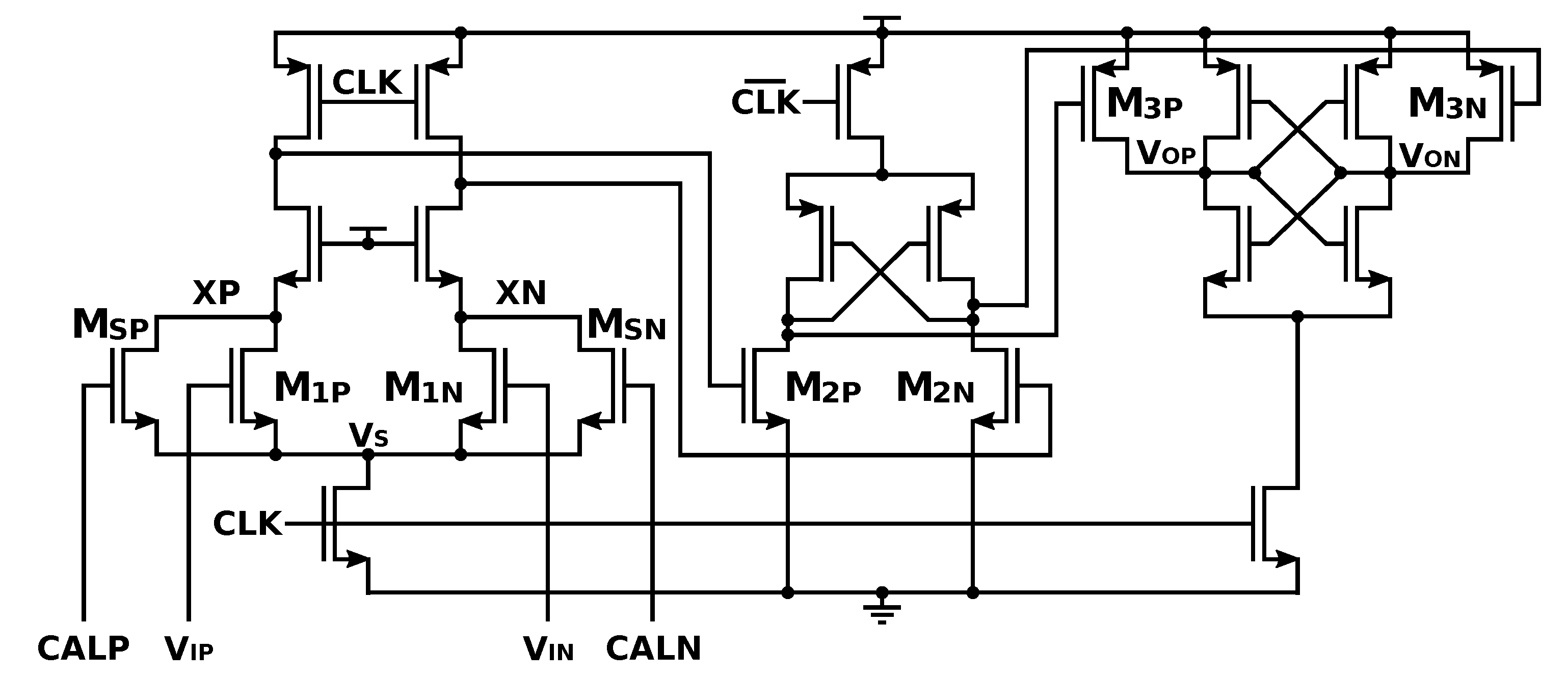
The schematic of the comparator circuit where the proposed calibration is employed is shown in
Figure 4. The comparator core incorporates a first amplification stage followed by a second amplifier/half latch and the final latch, in a fully-dynamic structure for low power operation [
24]. The multi-stage configuration allows for a more orthogonal optimization of each stage for various trade-offs, which allows the comparator to simultaneously achieve both high speed and low noise.
The required offset calibration pair
/
is connected in parallel to the main input pair
-
. The differential gate voltage of the extra pair is varied in the opposite direction to that of the main pair, in order to reverse the offset. This additional input pair leaks the charge from XP/XN without integration, which deteriorates the comparator noise performance. Therefore, the dimensioning of the offset canceling pair is an important trade-off in terms of noise and calibration range. Larger transistors result in a larger calibration range, but also larger charge leakage/noise. In this design, the sizes of
/
are chosen to be eight-times smaller than the main input pair
/
, to minimize the charge leakage, thus the noise degradation. This translates to a maximum of 125 mV offset compensation range (a
= 1 V in
Section 2) for a common-mode voltage of
V, which is large enough to allow a low-power and high-speed comparator design.
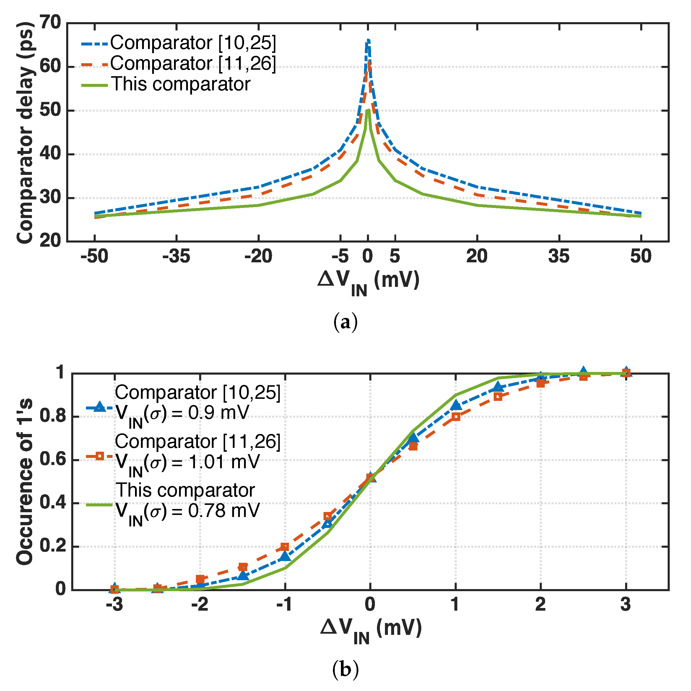
The implemented self-calibrating comparator performance in terms of delay and noise has been characterized with extracted simulations and compared to the comparators from [
10,
11,
25,
26], scaled to 28 nm (
Figure 5). For the comparator delay, the Overdrive Recovery Test (ORT) [
27,
28] has been used, while the noise has been characterized with both pss + pnoise and transient simulations. The operating conditions were
=
V and
=
V. The proposed design achieved more than 20% faster regeneration time for small inputs due to the increased gain in the signal path and showed a lower input dependency for a wide range of voltages compared to [
10,
11,
25,
26] (
Figure 5a). To achieve similar regeneration times, the tail, as well as the latching transistors of the works in [
10,
11,
25,
26] had to be upscaled, whose combined contribution increased the total input-referred noise by more than 15% with respect to this design, as shown in
Figure 5b.
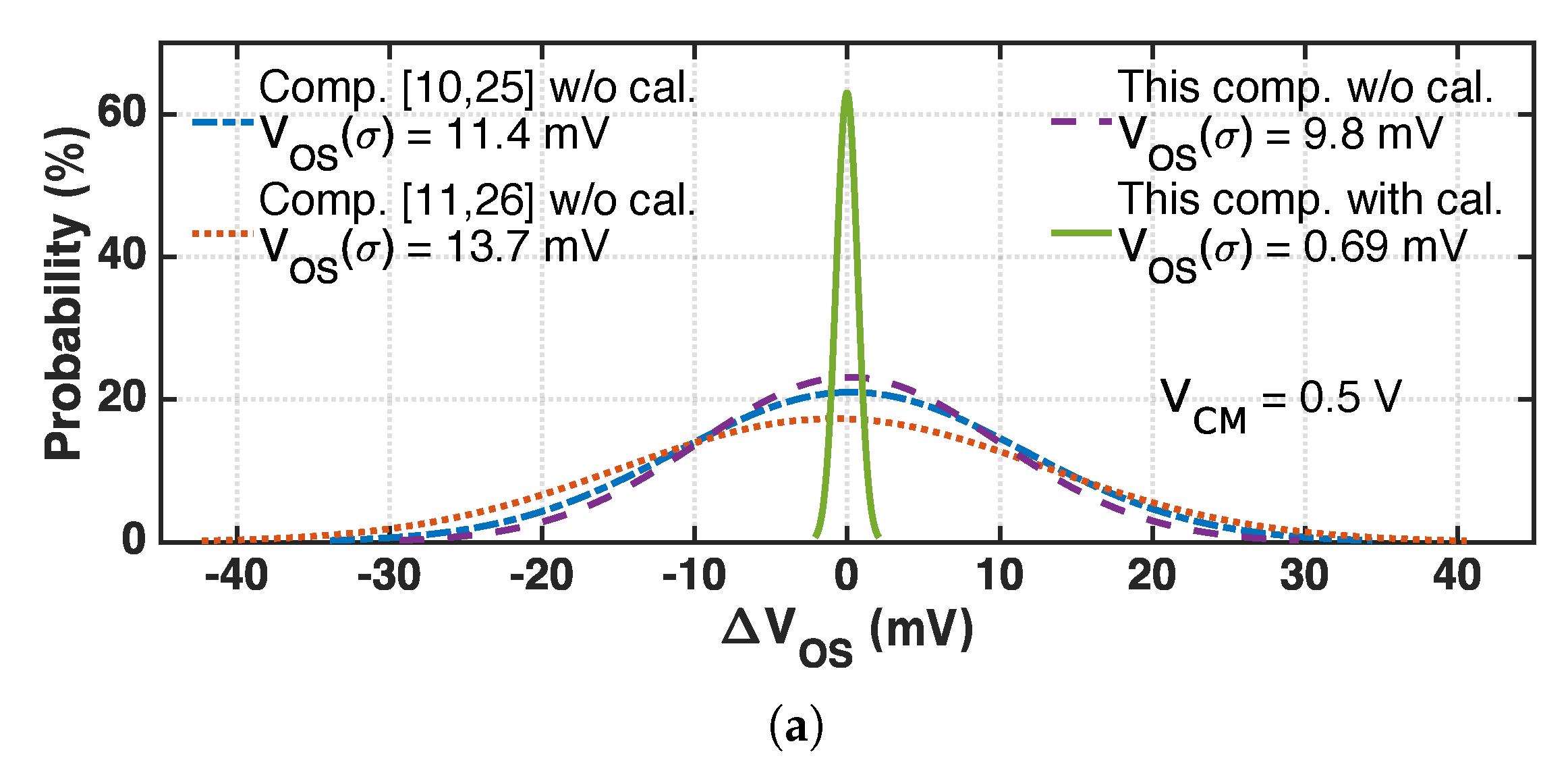
The offset for the three circuits with similar regeneration times has also been characterized through Monte Carlo simulations on 100 samples (
Figure 6). A servo-loop has been used, which senses the comparator output and feeds back to the input the opposite offset value until the comparator goes into a metastable state. For the designed V
CM of
V, the 1-σ raw value for both [
10,
11,
25,
26] was larger than 11 mV, while it was
mV for the proposed design (
Figure 6a). After enabling the proposed calibration, the offset was improved to
mV, set by the designed
/
ratio and noise, without compromising the rest of the specifications.
To show the effectiveness of the calibration for different common mode conditions, the comparator V
CM was varied between
V (
Figure 6b) and
V (
Figure 6c). It is seen that the accuracy of the calibration loop remained functional for a wide range of common mode voltages, dictated only by the comparator noise.
4. Experimental Results
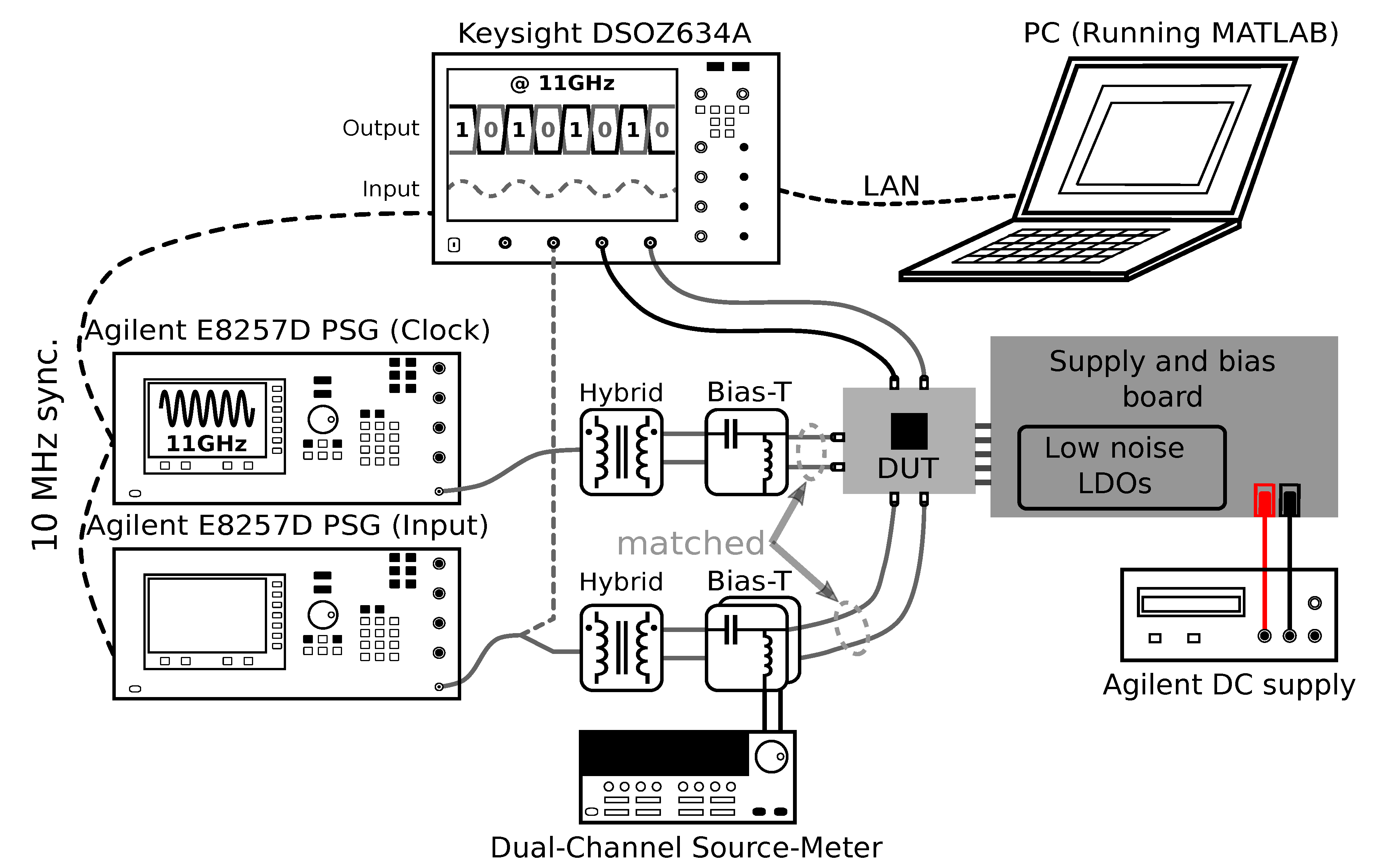
4.1. Measurement Setup
The measurement setup used to evaluate the comparator performance is shown in
Figure 7. A low phase noise signal source (Agilent E8257D) was used to generate the up to 11 GHz sinusoidal clock signal. This signal was converted into to a square pulse through on-chip CML + CMOS circuitry. An identical signal source was employed to generate the comparator input signal. Both input and clock signals were converted into differential signals by two identical wideband hybrids and AC-coupled to the chip through custom-designed bias-tees and phase-matched cables. A dual-channel source-meter was used to bias the differential comparator input, for easier noise and offset extraction.
The signal generators were locked together and with a 63 GHz bandwidth scope (DSOZ634A), serving as a data analyzer, which captured the differential output at full speed. The captured data were then processed on a PC in MATLAB. First, the comparator noise was characterized by observing the data, while the raw offset was subtracted from the comparator by applying different DC voltages from the source-meter. After noise characterization, the calibration loop was enabled and the calibrated comparator offset, as well as speed were evaluated.
The required supply and bias voltages for the different chip domains were generated with dedicated low-noise Low-Dropout Regulators (LDOs) on a custom bias board and provided to the chip after sufficient low-pass filtering.
4.2. Measurement Results
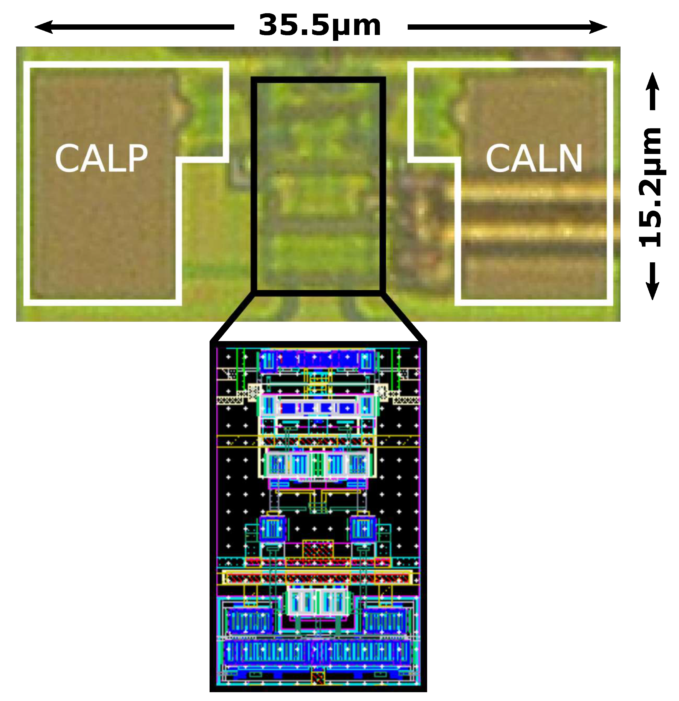
The prototype self-calibrating comparator was realized in a single-poly ten-metal (1P10M) 28 nm bulk CMOS process and occupied an area of 35.5 ×
µm
2 (
Figure 8). Most of the area was taken up by
/
, which is insignificant when used in an ADC. The measured power consumption of
mW at 1 V and 11 GHz clock frequency (
) partitions into
mW for the comparator core and only
mW for the calibration logic, less than 5% overhead.
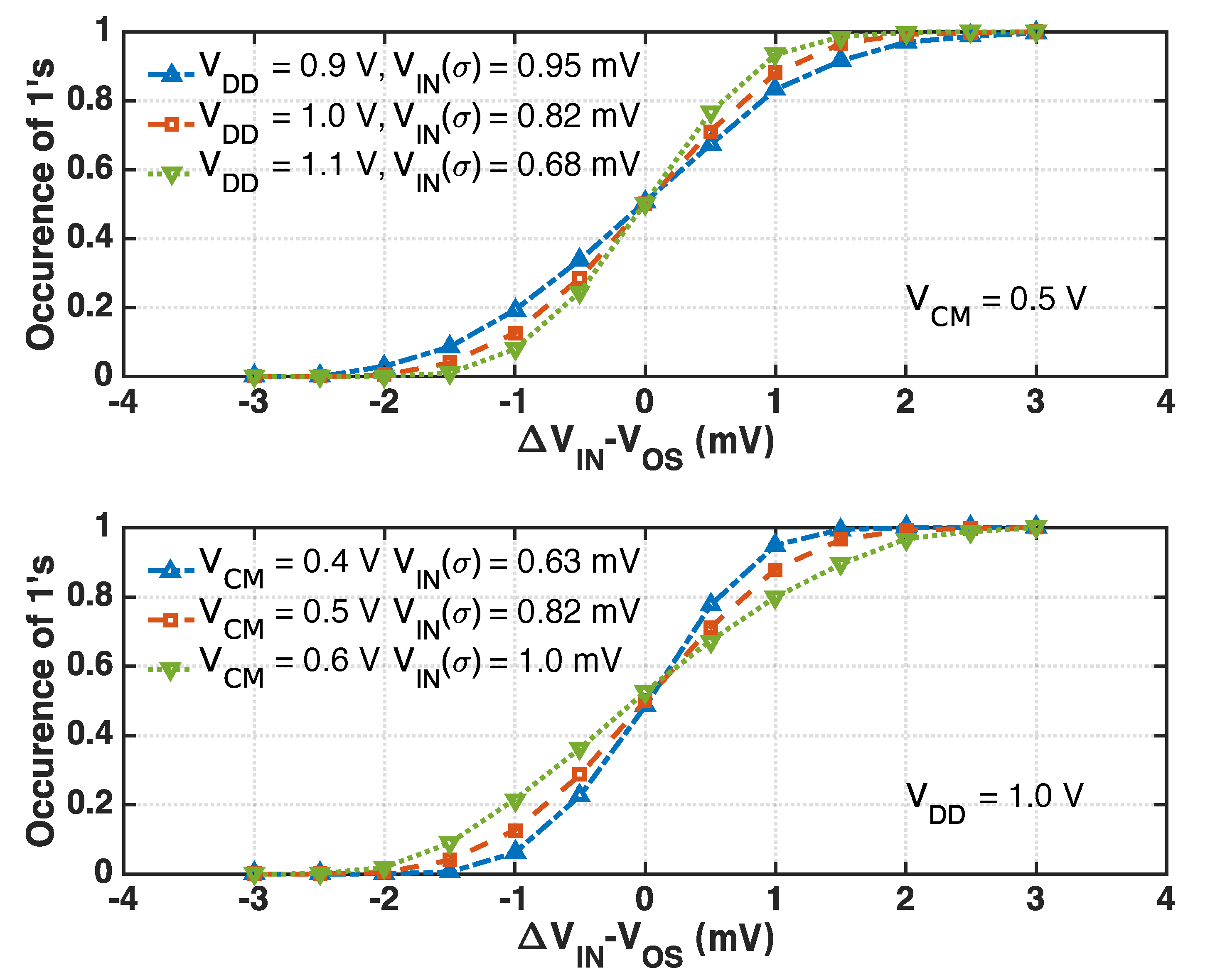
Figure 9 illustrates the measured input noise versus
when varying
(top) and
(bottom), respectively, at 11 GHz. The noise was extracted by counting the percentage of positive decisions with increasing the differential input voltage, having first subtracted the comparator offset. The calibration loop was disabled for this measurement. The comparator measured a 1-σ noise voltage of
mV
rms for
= 1 V and
=
V, which varied by only
mV when
changed from
V to
V and
mV when
changed from
V to
V.
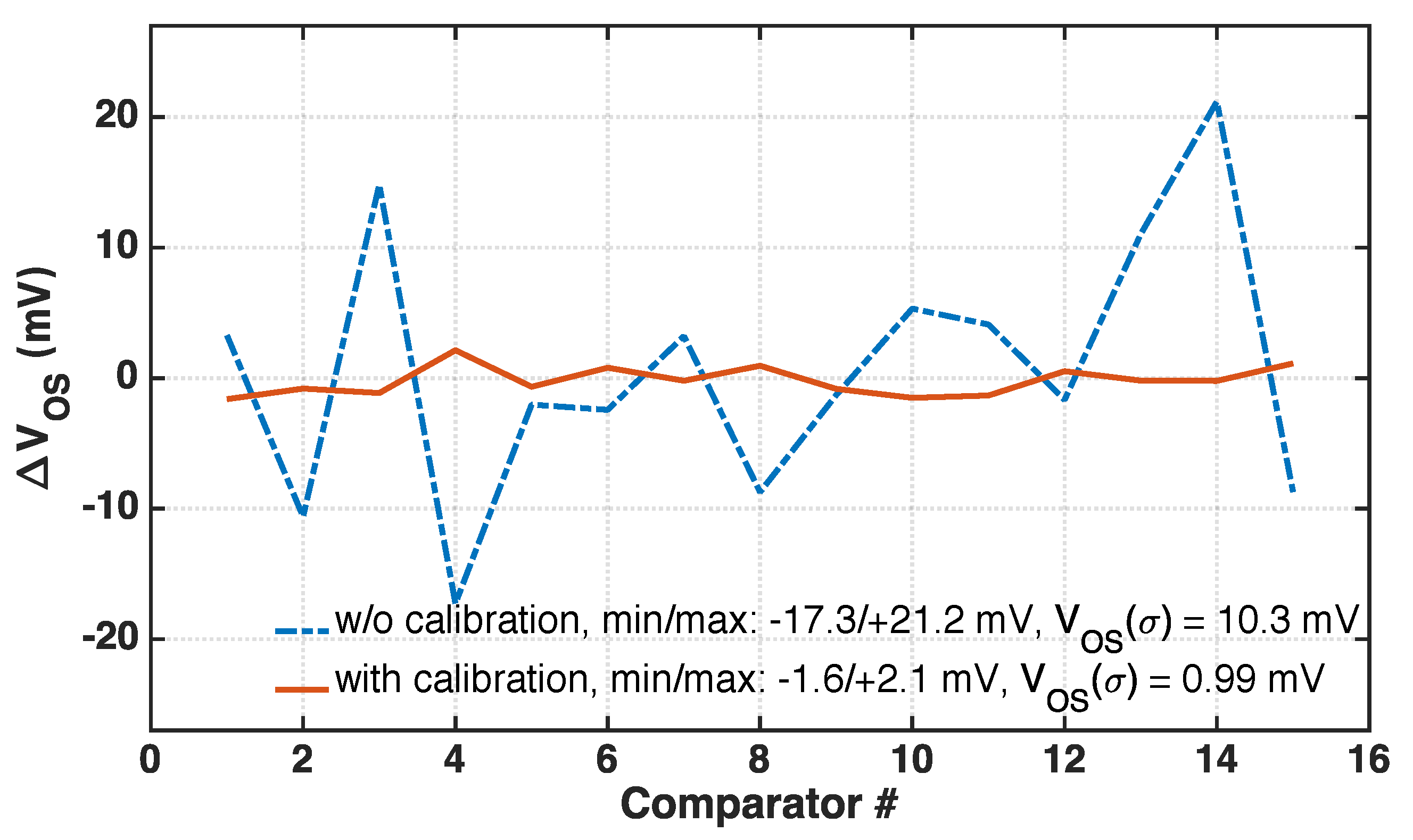
The offset voltage of the comparator was measured across 15 chips operating at 11 GHz with
=
V for the maximum compensation range (see
Section 3.2), as shown in
Figure 10. The offset was extracted by sweeping the input voltage of the comparator until the ratio of zeroes and ones was ∼50%. For the raw offset value, the calibration loop was disabled, while for the compensated value, the calibration was activated prior to collecting the data. Thanks to the proposed dual-sided calibration technique, the offset voltage was drastically reduced to
mV from the uncalibrated
mV (>10× improvement), without compromising the comparator speed, verifying its smooth integration in single- or multi-comparator ADCs. As expected, the calibration accuracy was ultimately limited by the comparator noise, which also matched nicely with the simulated results.
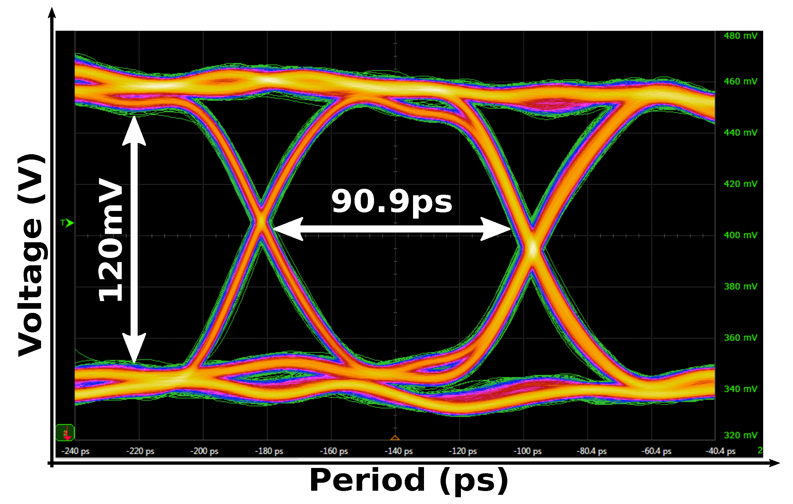
The maximum speed of the comparator for small inputs, close to the noise level, was characterized by observing the frequency above which increased differential input was required to preserve correct digital outputs. An eye diagram is shown in
Figure 11 for an
of 11 GHz and a coherent Nyquist sinusoidal input frequency of
GHz (= (8133/16,384) × 11 GHz), such that the comparator can capture any input voltage value over the full-scale range. With this setup, no metastability errors were detected for voltages outside the comparator noise levels, measured over one million time samples.
This work compares favorably with state-of-the-art comparators, summarized in
Table 1. This design achieved the highest reported operating frequency and the lowest delay slope, as well as the smallest sensitivity to V
DD and V
CM variations, compared to previously-measured published works. It also exhibited a very low input-referred noise and calibrated offset with state-of-the-art energy/comparison, demonstrating the effectiveness of the proposed calibration technique and its nearly zero overhead.
5. Conclusions
A high-speed, low-noise dynamic comparator with a dual-sided self-calibrating loop has been presented. The proposed dynamic calibration tremendously reduces the input offset by 10×, limited only by the comparator noise, without compromising its speed or significantly increasing its power. Combined with the implemented multi-stage comparator to enable better optimization between various trade-offs, the highest reported maximum frequency of 11 GHz is realized with only mV and mV input noise and offset, respectively, consuming only mW from a 1 V supply. The prototype occupies a total area of only 0.00054 mm2. In summary, the proposed circuit is an ideal candidate for any high speed, low noise/offset, power-/area-efficient mixed-signal system and can be adapted to any comparator structure. Moreover, its fully-dynamic implementation ensures 100% drawback-free scalability to lower technology nodes.
Future research will involve realizing a faster and lower noise comparator circuit to incorporate the proposed calibration loop. Finally, more transistor stacking will be employed in the circuit of
Figure 3 to realize a finer calibration step and reduce the leakage on CALP/CALN without increasing
/
.
Author Contributions
A.R. designed, simulated, taped-out, and measured the circuits described in this manuscript under the supervision of M.S. (Michiel Steyaert), and F.T. and M.S. (Maarten Strackx) contributed to the technical discussions during the design time.
Funding
This research was partially funded by Nokia Bell Labs, Antwerp, Belgium.
Acknowledgments
The authors would like to thank Nokia Bell Labs, Antwerp Belgium, for partially supporting this work.
Conflicts of Interest
The authors declare no conflicts of interest.
References
- Wang, Z.; Su, F.; Wang, Y.; Li, Z.; Li, X.; Yoshimura, R.; Naiki, T.; Tsuwa, T.; Saito, T.; Wang, Z.; et al. A 130 nm FeRAM-based parallel recovery nonvolatile SOC for normally-OFF operations with 3.9× faster running speed and 11× higher energy efficiency using fast power-on detection and nonvolatile radio controller. In Proceedings of the 2017 Symposium on VLSI Circuits, Kyoto, Japan, 5–8 June 2017; pp. C336–C337. [Google Scholar]
- Choi, S.; Huh, Y.; Park, S.; Yoon, K.; Bang, J.; Shin, S.; Ju, Y.; Yang, Y.; Yoon, J.; Ahn, C.; et al. A Quasi-Digital Ultra-Fast Capacitor-Less Low-Dropout Regulator Based on Comparator Control for x8 Current Spike of PCRAM Systems. In Proceedings of the 2018 IEEE Symposium on VLSI Circuits, Honolulu, HI, USA, 18–22 June 2018; pp. 107–108. [Google Scholar]
- Lee, C.; Lee, J.; Kim, K.; Heo, J.; Baek, J.; Cha, G.; Moon, D.; Lee, D.; Park, J.; Lee, S.; et al. Dual-Loop Two-Step ZQ Calibration for Dynamic Voltage–Frequency Scaling in LPDDR4 SDRAM. IEEE J. Solid-State Circuits 2018, 53, 2906–2916. [Google Scholar] [CrossRef]
- Norimatsu, T.; Kawamoto, T.; Kogo, K.; Kohmu, N.; Yuki, F.; Nakajima, N.; Muto, T.; Nasu, J.; Komori, T.; Koba, H.; et al. A 25 Gb/s multistandard serial link transceiver for 50 dB-loss copper cable in 28 nm CMOS. In Proceedings of the 2016 IEEE International Solid-State Circuits Conference (ISSCC), San Francisco, CA, USA, 31 January–4 February 2016; pp. 60–61. [Google Scholar]
- Aurangozeb; Hossain, A.K.M.D.; Hossain, M. Channel adaptive ADC and TDC for 28 Gb/s PAM-4 digital receiver. In Proceedings of the 2017 IEEE Custom Integrated Circuits Conference (CICC), Austin, TX, USA, 30 April–3 May 2017; pp. 1–4. [Google Scholar]
- Yi, I.; Chae, M.; Hyun, S.; Bae, S.; Choi, J.; Jang, S.; Kim, B.; Sim, J.; Park, H. A Time-Based Receiver With 2-Tap Decision Feedback Equalizer for Single-Ended Mobile DRAM Interface. IEEE J. Solid-State Circuits 2018, 53, 144–154. [Google Scholar] [CrossRef]
- Gandara, M.; Guo, W.; Tang, X.; Chen, L.; Yoon, Y.; Sun, N. A pipelined SAR ADC reusing the comparator as residue amplifier. In Proceedings of the 2017 IEEE Custom Integrated Circuits Conference (CICC), Austin, TX, USA, 30 April–3 May 2017; pp. 1–4. [Google Scholar]
- Shim, M.; Jeong, S.; Myers, P.D.; Bang, S.; Shen, J.; Kim, C.; Sylvester, D.; Blaauw, D.; Jung, W. Edge-Pursuit Comparator: An Energy-Scalable Oscillator Collapse-Based Comparator With Application in a 74.1 dB SNDR and 20 kS/s 15 b SAR ADC. IEEE J. Solid-State Circuits 2017, 52, 1077–1090. [Google Scholar] [CrossRef]
- Ding, Z.; Zhou, X.; Li, Q. A 0.5–1.1 V 10 B Adaptive Bypassing SAR ADC Utilizing Oscillation Cycle Information of VCO-Based Comparator. In Proceedings of the 2018 IEEE Symposium on VLSI Circuits, Honolulu, HI, USA, 18–22 June 2018; pp. 93–94. [Google Scholar]
- Wicht, B.; Nirschl, T.; Schmitt-Landsiedel, D. Yield and speed optimization of a latch-type voltage sense amplifier. IEEE J. Solid-State Circuits 2004, 39, 1148–1158. [Google Scholar] [CrossRef]
- Schinkel, D.; Mensink, E.; Klumperink, E.; van Tuijl, E.; Nauta, B. A Double-Tail Latch-Type Voltage Sense Amplifier with 18 ps Setup+Hold Time. In Proceedings of the 2007 IEEE International Solid-State Circuits Conference. Digest of Technical Papers, San Francisco, CA, USA, 11–15 February 2007; pp. 314–605. [Google Scholar]
- Rabbi, F.; Das, S.; Hossain, Q.D.; Pathan, N.S. Design of a Low-Power Ultra High Speed Dynamic Latched Comparator in 90-nm CMOS Technology. In Proceedings of the 2018 International Conference on Computer, Communication, Chemical, Material and Electronic Engineering (IC4ME2), Rajshahi, Bangladesh, 8–9 February 2018; pp. 1–4. [Google Scholar]
- Rezapour, A.; Shamsi, H.; Abbasizadeh, H.; Lee, K. Low Power High Speed Dynamic Comparator. In Proceedings of the 2018 IEEE International Symposium on Circuits and Systems (ISCAS), Florence, Italy, 27–30 May 2018; pp. 1–5. [Google Scholar]
- Aiello, O.; Crovetti, P.; Alioto, M. Fully Synthesizable, Rail-to-Rail Dynamic Voltage Comparator for Operation down to 0.3 V. In Proceedings of the 2018 IEEE International Symposium on Circuits and Systems (ISCAS), Florence, Italy, 27–30 May 2018; pp. 1–5. [Google Scholar]
- Pelgrom, M.J.M.; Duinmaijer, A.C.J.; Welbers, A.P.G. Matching properties of MOS transistors. IEEE J. Solid-State Circuits 1989, 24, 1433–1439. [Google Scholar] [CrossRef]
- Pelgrom, M. Analog-to-Digital Conversion, 3rd ed.; Springer: Berlin, Germany, 2017. [Google Scholar]
- Krämer, M.; Janssen, E.; Doris, K.; Murmann, B. A 14-Bit 30-MS/s 38-mW SAR ADC Using Noise Filter Gear Shifting. IEEE Trans. Circuits Syst. II 2017, 64, 116–120. [Google Scholar] [CrossRef]
- Verbruggen, B.; Iriguchi, M.; Craninckx, J. A 1.7 mW 11 b 250 MS/s 2x interleaved fully dynamic pipelined SAR ADC in 40 nm digital CMOS. In Proceedings of the 2012 IEEE International Solid-State Circuits Conference, San Francisco, CA, USA, 19–23 February 2012; pp. 466–468. [Google Scholar]
- Vaz, B.; Lynam, A.; Verbruggen, B.; Laraba, A.; Mesadri, C.; Boumaalif, A.; Mcgrath, J.; Kamath, U.; Torre, R.D.L.; Manlapat, A.; et al. 16.1 A 13b 4GS/s digitally assisted dynamic 3-stage asynchronous pipelined-SAR ADC. In Proceedings of the 2017 IEEE International Solid-State Circuits Conference (ISSCC), San Francisco, CA, USA, 5–9 February 2017; pp. 276–277. [Google Scholar]
- Vaz, B.; Verbruggen, B.; Erdmann, C.; Collins, D.; Mcgrath, J.; Boumaalif, A.; Cullen, E.; Walsh, D.; Morgado, A.; Mesadri, C.; et al. A 13 Bit 5 GS/S ADC with Time-Interleaved Chopping Calibration in 16 NM FinFET. In Proceedings of the 2018 IEEE Symposium on VLSI Circuits, Honolulu, HI, USA, 18–22 June 2018; pp. 99–100. [Google Scholar]
- Miyahara, M.; Asada, Y.; Paik, D.; Matsuzawa, A. A low-noise self-calibrating dynamic comparator for high-speed ADCs. In Proceedings of the 2008 IEEE Asian Solid-State Circuits Conference, Fukuoka, Japan, 3–5 November 2008; pp. 269–272. [Google Scholar]
- Chan, C.H.; Zhu, Y.; Chio, U.F.; Sin, S.W.; Seng-Pan, U.; Martins, R.P. A reconfigurable low-noise dynamic comparator with offset calibration in 90 nm CMOS. In Proceedings of the IEEE Asian Solid-State Circuits Conference, Jeju, Korea, 14–16 November 2011; pp. 233–236. [Google Scholar]
- Chan, C.; Zhu, Y.; Ho, I.; Zhang, W.; Seng-Pan, U.; Martins, R.P. A 5 mW 7 b 2.4 GS/s 1-then-2b/cycle SAR ADC with background offset calibration. In Proceedings of the 2017 IEEE International Solid-State Circuits Conference (ISSCC), San Francisco, CA, USA, 5–9 February 2017; pp. 282–283. [Google Scholar]
- Ramkaj, A.; Strackx, M.; Steyaert, M.; Tavernier, F. A 36.4 dB SNDR @ 5 GHz 1.25 GS/s 7 b 3.56 mW single-channel SAR ADC in 28 nm bulk CMOS. In Proceedings of the ESSCIRC 2017 43rd IEEE European Solid State Circuits Conference, Leuven, Belgium, 11–14 September 2017; pp. 167–170. [Google Scholar]
- Luu, D.; Kull, L.; Toifl, T.; Menolfi, C.; Brändli, M.; Francese, P.A.; Morf, T.; Kossel, M.; Yueksel, H.; Cevrero, A.; et al. A 12-bit 300-MS/s SAR ADC With Inverter-Based Preamplifier and Common-Mode-Regulation DAC in 14-nm CMOS FinFET. IEEE J. Solid-State Circuits 2018, 53, 3268–3279. [Google Scholar] [CrossRef]
- Bindra, H.S.; Lokin, C.E.; Annema, A.; Nauta, B. A 30fJ/comparison dynamic bias comparator. In Proceedings of the ESSCIRC 2017 43rd IEEE European Solid State Circuits Conference, Leuven, Belgium, 11–14 September 2017; pp. 71–74. [Google Scholar]
- Razavi, B. Principles of Data Conversion System Design; Wiley-IEEE Press: New York, NY, USA, 1995. [Google Scholar]
- Nasrollahpour, M.; Yen, C.; Hamedi-hagh, S. A high-speed, low-offset and low-power differential comparator for analog to digital converters. In Proceedings of the 2017 International SoC Design Conference (ISOCC), Seoul, Korea, 5–8 November 2017; pp. 220–221. [Google Scholar]
- Goll, B.; Zimmermann, H. A 65 nm CMOS comparator with modified latch to achieve 7 GHz/1.3 mW at 1.2 V and 700 MHz/47 µW at 0.6 V. In Proceedings of the 2009 IEEE International Solid-State Circuits Conference—Digest of Technical Papers, San Francisco, CA, USA, 8–12 February 2009; pp. 328–329. [Google Scholar]
- Abbas, M.; Furukawa, Y.; Komatsu, S.; Takahiro, J.Y.; Asada, K. Clocked comparator for high-speed applications in 65 nm technology. In Proceedings of the 2010 IEEE Asian Solid-State Circuits Conference, Beijing, China, 8–10 November 2010; pp. 1–4. [Google Scholar]
- Kong, L.; Lu, Y.; Alon, E. A multi-GHz area-efficient comparator with dynamic offset cancellation. In Proceedings of the 2011 IEEE Custom Integrated Circuits Conference (CICC), San Jose, CA, USA, 17–20 September 2011; pp. 1–4. [Google Scholar]
© 2018 by the authors. Licensee MDPI, Basel, Switzerland. This article is an open access article distributed under the terms and conditions of the Creative Commons Attribution (CC BY) license (http://creativecommons.org/licenses/by/4.0/).


