1. Introduction
Reed–Solomon (RS) error-correction codes are widely used in communication and storage systems due to their capacity to correct both burst errors and random errors. These codes are being incorporated in recent 100 Gbps Ethernet standards over a four-lane backplane channel, as well as over a four-lane copper cable [
1,
2], and for optical fiber cables. Generally, the main decoding methods for RS codes are divided into hard-decision decoding (HDD) and algebraic soft-decision (ASD) decoding. The hard-decision RS decoder architecture consists, commonly, of three main computation blocks: syndrome computation, key equation solver and error location and evaluation. In a different way, ASD algorithms require three main steps: multiplicity assignment (MA), interpolation and factorization. ASD algorithms can achieve significant coding gain at a cost of a small increase in complexity when compared with HDD. Low-Complexity Chase (LCC) [
3,
4] achieves the same error correction performance with lower complexity, when compared to other Algebraic Soft-Decision Decoding algorithms [
5,
6,
7] for Reed–Solomon codes [
8], like bit-level generalized minimum distance (BGMD) decoding [
9] or Kötter–Vardy (KV) [
5]. The main benefit of LCC is the use of just one level of multiplicity, which means that only the relationship between the hard-decision (HD) reliability value of the received symbols and the second best decision is required to exploit the soft-information from the channel. This fact has a great impact on the number of iterations and on the global complexity of the interpolation and factorization steps [
10,
11,
12,
13,
14,
15,
16] compared to KV and BGMD [
17]. Another benefit derived from having just one level of multiplicity is that the interpolation and factorization stages can be replaced by Berlekamp–Massey decoders [
18], and this results in a considerable reduction in the total number of operations [
19].
Recently, Peng et al. [
20] showed that the computation of the symbol reliability values can be performed using bit-level magnitudes. They also presented implementation results for a soft-decision decoder that includes the Multiplicity Assignment stage (MAS). On the other hand, Lin et al. [
21] proposed a decoder that reduces the complexity by relaxing the criteria for the selection of the best test vector. The resulting decoder requires less area than decoders with worse performance.
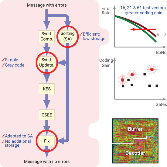
The main contributions of the present paper are as follows. We present a novel MAS based on the one proposed in [
20], which sorts and stores less data than in that proposal. We propose also novel implementation schematics for the Syndrome Update (SUS) and Symbol Modification (SMS) stages that are adapted to the proposed MAS. We also propose a scalable architecture for the computation of a high number of test vectors, therefore, it reaches high coding gain. We detail two architectures that use two or four Key Equation Solver (KES) blocks, and follow a Gray code sequence to process the test vectors, so the complexity of the decoder is not increased. Specifically, we present three decoders for soft-decision RS decoding. The first is a
LCC decoder. The other two, which we call Q5 and Q6, do not decode the complete set of
test vectors of
and
LCC decoders, but only a subset of them. The proposed decoders give a solution for the problems created by using a high number of test vectors, since, in that case, the design of the decoder is not as simple as parallelizating resources. We present implementation results for FPGA and CMOS ASIC devices that confirm that our proposals have lower area while they achieve higher coding gain than state-of-the-art decoders.
The organization of this paper is as follows. In
Section 2 and
Section 3 we summarize the background concepts about RS and LCC decoding, respectively. In
Section 4 we detail the architecture for the proposed decoders. The implementation results and comparisons are given in
Section 5. Finally, in
Section 6 we present the conclusions.
2. RS Decoders
In an RS(N,K) code over GF(), where , redundant symbols are added to the K-symbol message to obtain the N-symbol codeword . After the codeword is transmitted over a noisy channel, the decoder receives , where is the noise polynomial.
The RS decoding process begins with the Syndrome Computation (SC) block. This block computes the syndromes that are the coefficients of the syndrome polynomial . This is achieved by evaluating the received polynomial in the roots of the generator polynomial, specifically for , where is the primitive element of GF(). The KES block obtains the error-locator and the error magnitude polynomials by solving the key-equation . The third block is the Chien Search and Error Evaluation (CSEE). The Chien search finds the error locations, evaluating in all the possible positions (i.e., ), for ) and an error evaluation method (e.g., Forney’s formula) is used to calculate the error magnitude (e.g., when the Chien search finds an error location, which is whenever . If the total amount of errors in does not exceed the error correcting capability t, all the errors in are corrected subtracting the error magnitudes from the received symbols.
3. Low-Complexity Chase Decoder
We assume that the codeword C is modulated in binary phase-shift keying (BPSK) and transmitted over a Gaussian Noise (AWGN) channel. The LCC algorithm uses the reliability of the received symbols in order to generate a set of test vectors that will be decoded with a HD decoder (HDD). The reliability of a symbol is derived from the a posteriori probabilities , but instead, the likelihood function, , can be used by applying Bayes’ Law. The reliability of the received symbol is defined as , where is the symbol with the highest probability of being the transmitted symbol for the i-th received symbol and is the symbol with the second highest probability.
The closer
is to zero, the less reliable
is, since the probabilities of being
or
the transmitted symbol are more similar. Once
is computed for all the received symbols, those
symbols with the smallest values of
are selected, where
is a positive integer. The LCC decoding process creates
different test vectors: all the possible combinations of choosing or not
instead of
for those
symbols. As proposed in [
20],
is obtained by flipping the least reliable bit of
.
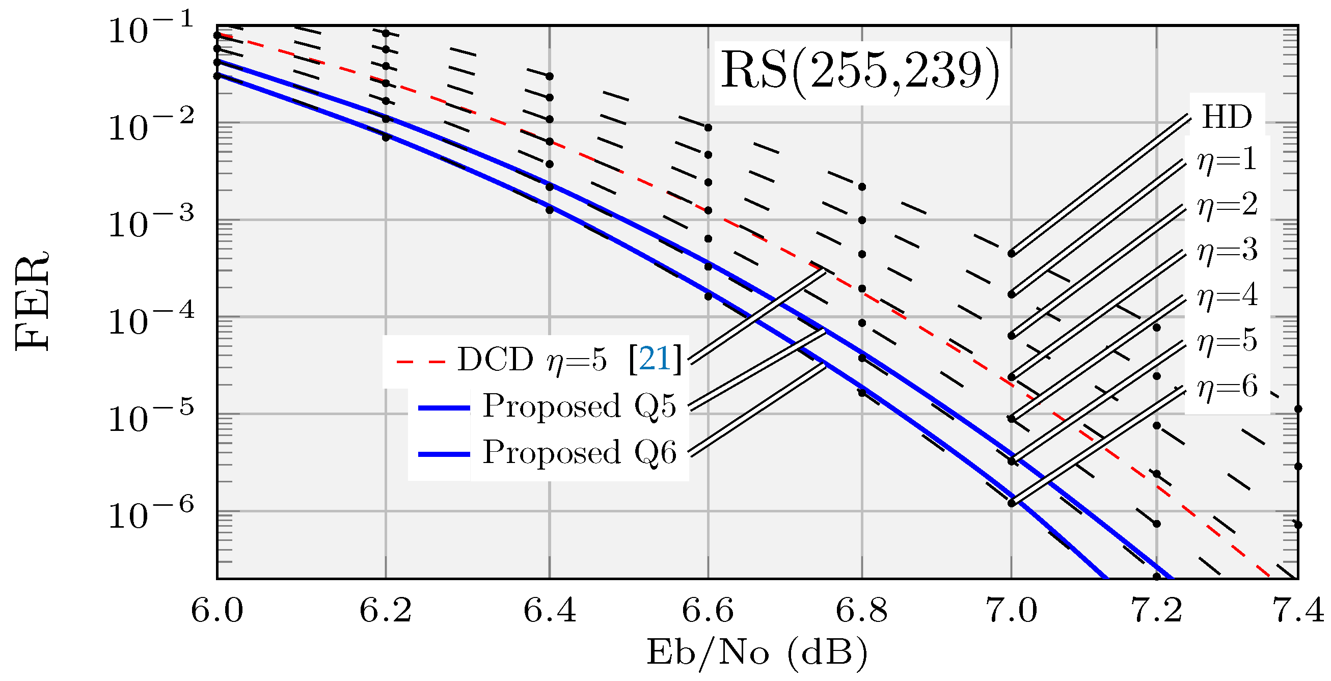
The Frame Error Rate performance of the RS(255,239) LCC decoder is shown in
Figure 1 for
.
4. Decoder Architecture
In this section we present the architecture for three soft-decision RS(255,239) decoders. The first decoder we present is a
LCC. The second one, which we refer to as Q5, is a quasi-
LCC: it uses all the test vectors of a true
LCC, but one. The third one, which we refer to as Q6, is a quasi-
LCC: it uses all the test vectors of a true
LCC, but four. They are based on a systolic KES, the enhanced parallel inversionless Berlekamp–Massey algorithm (ePiBMA) [
22], that requires
cycles for the computation of each frame, with low critical path: one adder (T
), one multiplexer (T
) and one multiplier (T
). Moreover, the selected KES requires fewer resources than other popular options. If the computation times of the three main pipeline stages are equalized, one KES can be used to compute 16 test vectors, for example for a
LCC decoder. For the Q5/Q6 decoders we propose the use of 2/4 KES working in parallel, which increases the decoding capability to 32/64 test vectors.
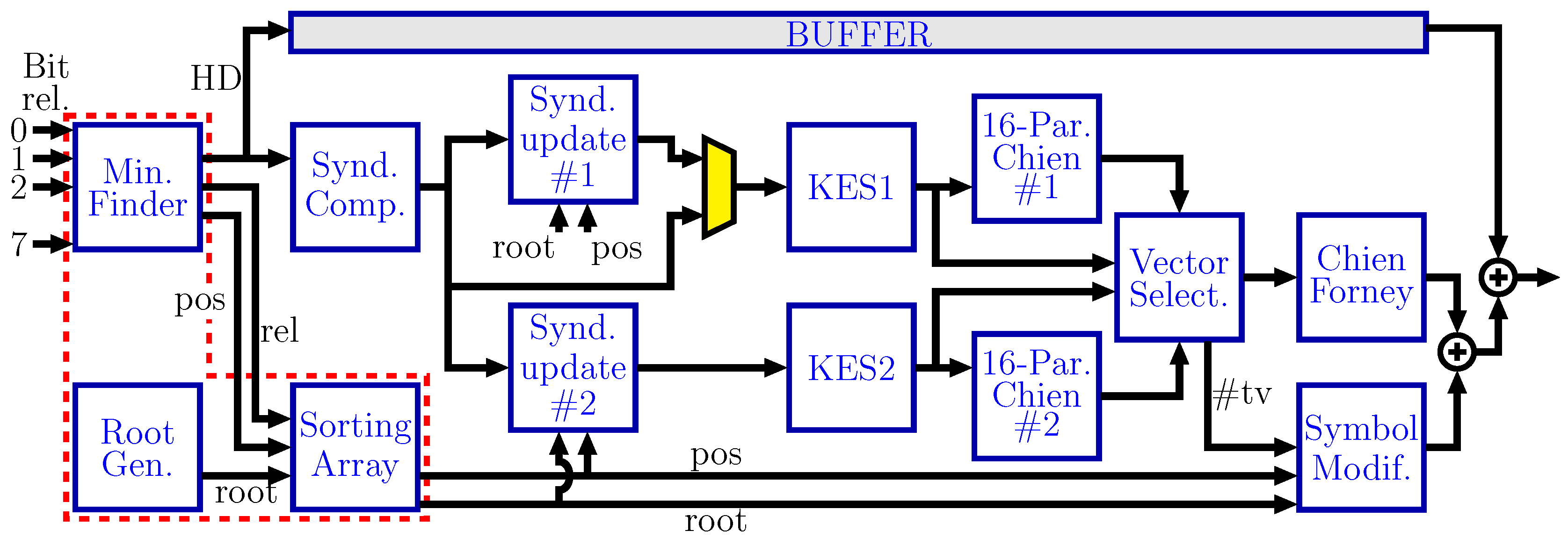
Figure 2 shows the block diagram for the proposed Q5 decoder. The decoder is based on the three classical blocks of a HDD: SC, KES and CSEE. Furthermore, more functional blocks are required to manage the additional test vectors. First, the test vectors have to be created and their relevant characteristics are stored so the rest of the blocks can process those test vectors. A tree of comparators and multiplexers finds the least reliable bit of each symbol. The Sorting Array block, as described below, selects the
least reliable symbols of the received frame, which are sorted and stored for later use. The SC block computes the syndromes for the HD test vector and that information is used to create the syndromes for the additional test vectors. Each KES is fed with the syndromes of a new test vector each 16 cycles. The 16 Parallel Chien Polynomial Evaluation (PCPE) blocks are used to anticipate if those test vectors will be successfully decoded in a full CSEE block. After all those computations, the Vector Selection stage (VSS) feeds the CSEE block with the best test vector available. The vector test selection criteria are as follows: the first vector that accomplishes that the number of errors is equal to the order of the error-locator polynomial is the one to be decoded; otherwise, the HD test vector is selected.
In the case of
, one KES is enough to process all the test vectors and, therefore, the block diagram is the same as in
Figure 2 but without KES2, SUS2 and PCPE2. In the case of the Q6 decoder, two more copies of each of those three blocks are required.
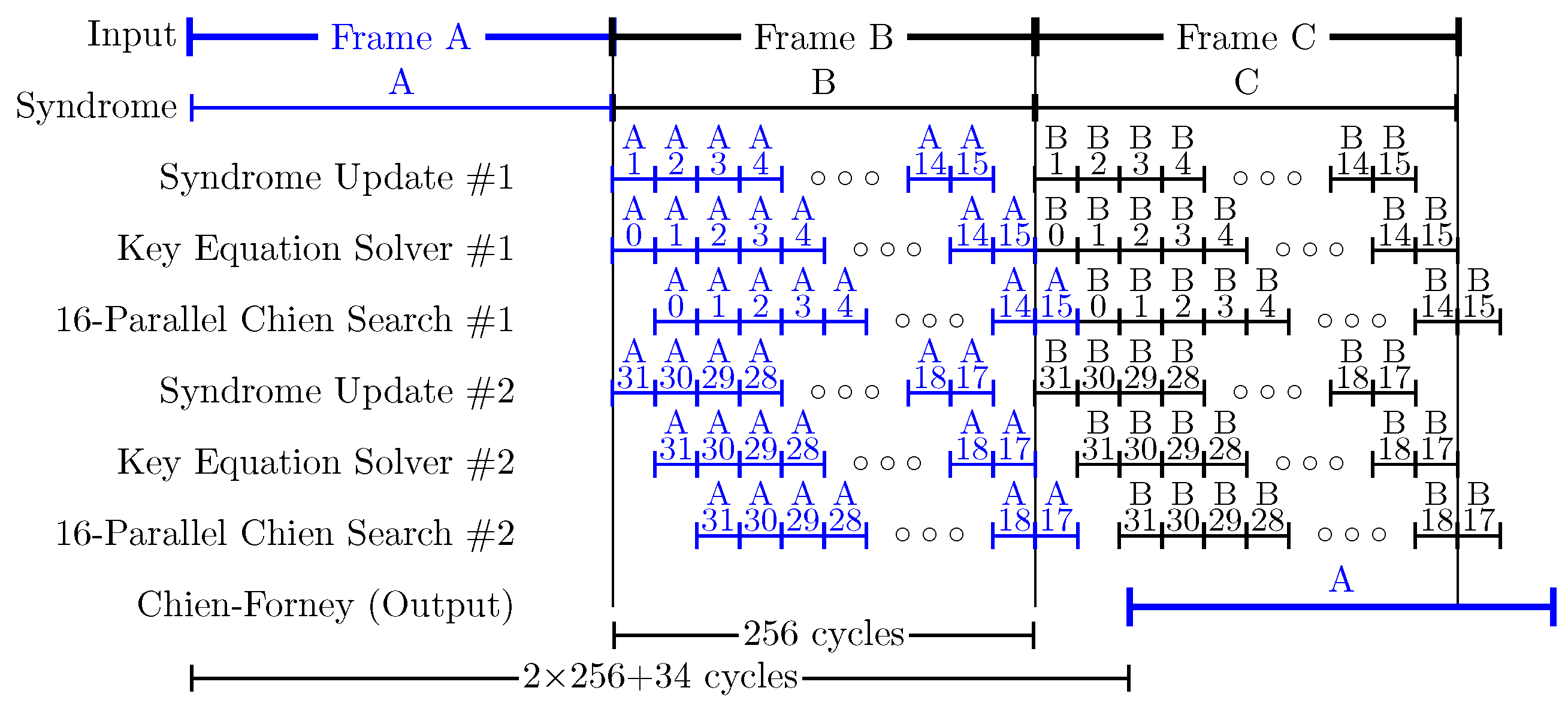
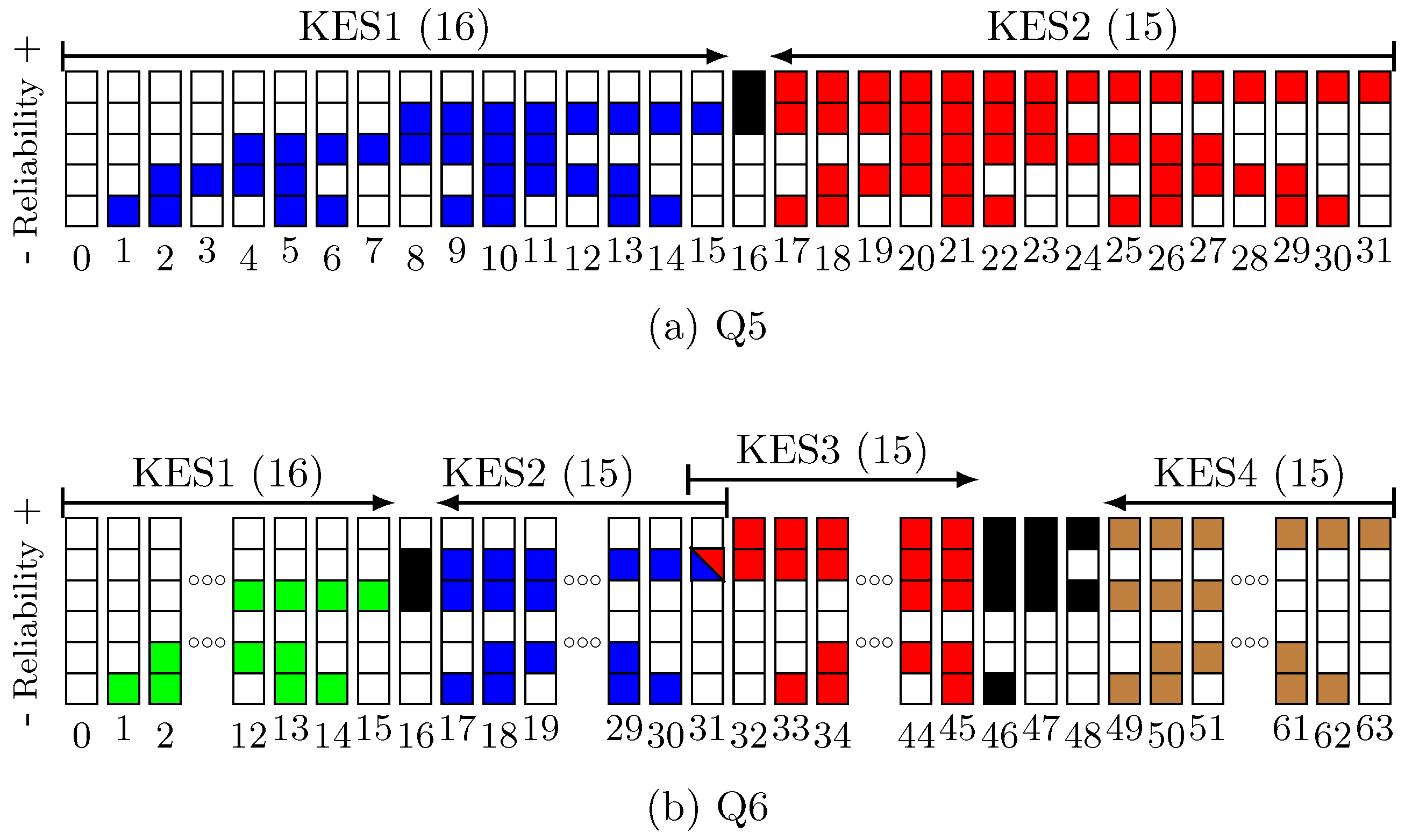
Figure 3 shows the decoding chronogram for the Q5 decoder. As can be seen, while a KES computes a specific test vector, the corresponding SUS calculates the syndromes for the next one. At the same time, the corresponding PCPE processes the previous test vector. The decoding of a new frame can start every 256 cycles. In this decoder, KES2 must wait 16 cycles until the syndromes for its first test vector (i.e., #31) are available. KES1, on the other hand, works with test vector #0 (HD) during those cycles, since its syndromes are available. If KES2 were to compute 16 test vectors, the latency of the decoder would increase, since the decisions in VSS would be delayed. Moreover, the complexity of the decoder would also increase because the control logic would have to consider decisions for two consecutive frames at the same time. Therefore, Q5 computes 31 out of the 32 possible test vectors of a
LCC (see
Figure 4a). The test vectors that are evaluated by each KES follow a Gray code sequence. This allows the syndromes for a test vector to be easily created from the syndromes of the previous one [
19]. The total amount of required operations is reduced, since only one symbol changes from one test vector to the next one. It should be noted that the first test vector evaluated by each KES and the HD frame are different in just one symbol. Note that SUS2 follows the Gray sequence in reverse order, starting with test vector #31. In Q6, for the same reasons explained above, only
test vectors could be decoded. Nevertheless, in order to start the computation in all four KES with a test vector that has only one symbol difference with respect to the HD frame, we compute test vector #31 simultaneously in two KES, as shown in
Figure 4b. Therefore, Q6 computes 60 out of the 64 possible test vectors in
. For the
LCC, the full 4-bit Gray sequence is decoded. As can be observed in
Figure 1, the coding gain of decoders Q5 and Q6 is close to that of true
and
decoders, respectively.
In the following subsections, we describe the blocks that are different from the ones in other LCC decoders.
4.1. Multiplicity Assignment Block
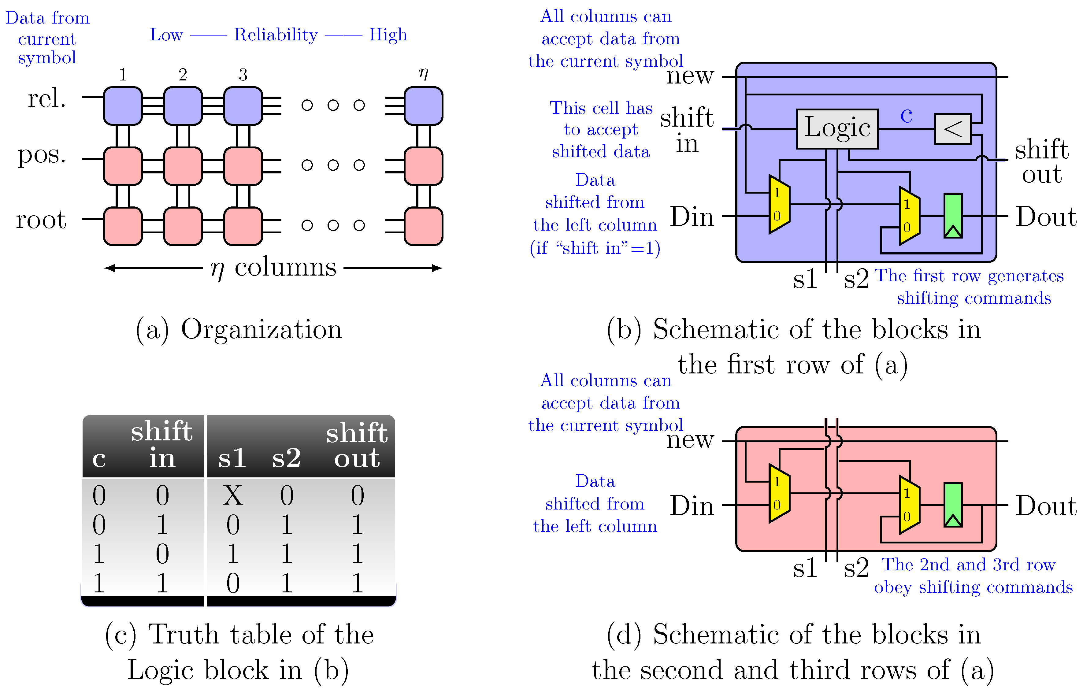
The Minimum Finder block receives the soft magnitudes of the
bits of a symbol and sorts them according to their absolute value [
20]. For each symbol of the received frame this block outputs the hard decision value, the absolute value of the least reliable bit of the symbol and its position in the symbol (a 3-bit value). The goal of the Sorting Array block is to provide all the information required to create the additional test vectors. The information we need to create the test vectors is the position of each one of these
symbols in the frame and the location of their least reliable bit inside those symbols. In [
20] both
and
are sorted and stored for the
least reliable symbols. Nevertheless, in our proposal, instead of sorting/storing
8-bit values, we only sort/store
3-bit values that are the positions of the least reliable bits in the symbols. It is unnecessary to store
and
since
is already stored in the buffer and
can be obtained from
if the position of its least reliable bit,
, is known, since
. Assuming that the reliability values are stored with
g bits, a total of
bit registers are required in our proposal, whereas in [
20]
bit registers are required.
Moreover, instead of sorting/storing the positions of the symbols in the frames, for convenience reasons that are explained below, we sort/store the corresponding powers of
created by the Root Generator block.
Figure 5a shows the architecture of the Sorting Array block. The first row uses the output from the Minimum Finder block to sort the symbols according to their reliability. The other 2 rows of the schematic apply the decisions adopted in the first block of their column and, therefore, store the position of the least reliable bits inside their symbol and the location of the symbols inside the frame.
Figure 5b,d show the implementation schematic of the basic blocks in
Figure 5a. The pseudocode of the Sorting Array block is shown in Algorithm 1.
| Algorithm 1 Pseudocode for the Sorting Array block |
| Input: For every symbol location in the frame and its bit , the Min. Finder block provides and (where are the bit-level received voltages) |
| begin |
| Step 1 Sort symbols of the frame according to . |
| Step 2 = symbol locations of the symbols with lowest |
| Step 3 |
| for | // for all symbols selected in Step 2 |
| | // root associated with its position in the frame |
| | // location of the least reliable bit in the symbol |
| end |
| end |
| Output: root,pos |
4.2. Syndrome Update Block
The value to be added to the previous
i-th syndrome,
, to obtain the new
i-th syndrome,
, is:
where
j is the position of the symbol in the frame and
is the position of its least reliable bit.
In this work, we propose a novel architecture for SUS that takes advantage of Equation (
1) and of the fact of storing powers of
to indicate the positions of the least reliable symbols in the frame instead of their positions itself.
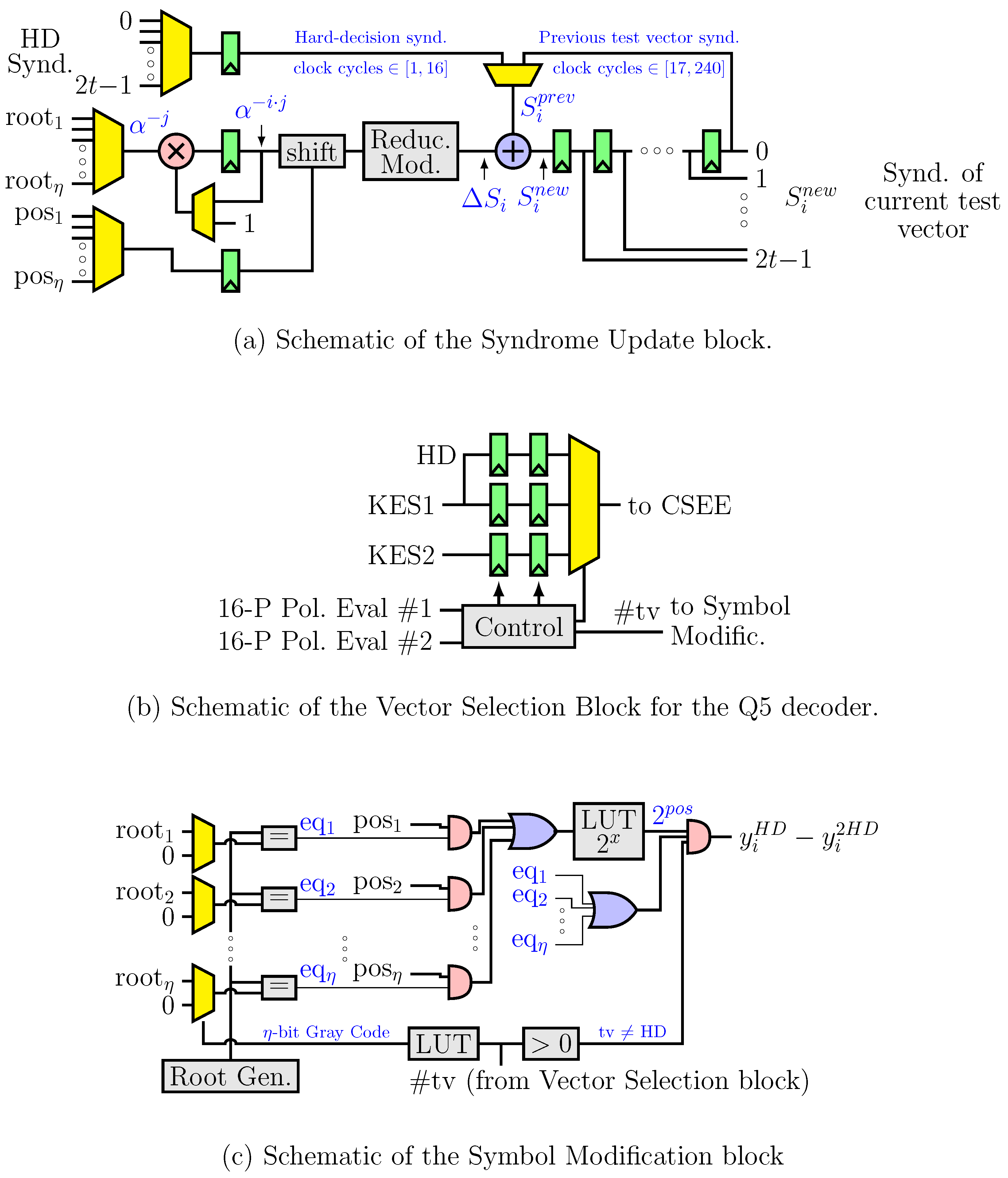
Figure 6a shows the schematic of this block. The root multiplexer outputs
(selected from root
–root
). The pos multiplexer outputs
(selected from pos
–pos
). Both values are changed each 16 clock cycles. The shift block scales by
and the Reduction Modulo block computes the modular reduction to the primitive polynomial of the Galois Field. One syndrome is updated each clock cycle. For the first 16 clock cycles, the HD syndromes are used to compute the new syndromes. After that, the syndromes are computed from the syndromes of the previous test vector. The pseudocode of the Syndrome Update block is shown in Algorithm 2.
| Algorithm 2 Pseudocode for the Syndrome Update block |
| Input: root and pos from the Sorting Array block, and hard-decision syndromes from the |
| Syndrome Computer |
| begin |
| for all the test vectors (tv) assigned to this block |
| h=index in root of the symbol that is different from previous tv |
| | // |
| |
| for | // for all the syndromes |
| if tv = first test vector (one with 1 symbol change from HD) |
| |
| end |
| | // |
| |
| |
| end |
| Output: | // syndromes for the current test vector |
| end |
| end |
4.3. Vector Selection Block
This block selects the test vector whose KES output feeds the CSEE block. The decision depends on whether the number of errors found by the PCPE block matches the order of the error-locator polynomial. Since the latency of the PCPE block is 21 (which is greater than the latency of the KES), VSS requires that the KES output from the previous test vector is still available. Therefore, for each KES in the decoder, two sets of registers are required to store the current and the previous test vectors. On the other hand, since the decision to feed the CSEE block with HD may be delayed beyond the moment a new frame is being received (see
Figure 3), the KES output for HD requires also two sets of registers to save the current and the previous frames. VSS also outputs the identification number of the test vector that is selected. The schematic for the VSS of the Q5 decoder is shown in
Figure 6b. For the
LCC the schematic is similar, but there is neither KES2 nor a second polynomial evaluation block. In the case of the Q6 decoder, more registers should be added for the storage of the KES3 and KES4 outputs, just as shown in
Figure 6b for KES2.
4.4. Symbol Modification Block
In an HDD, the corrected frame is created from the received frame and the error information. but in a LCC decoder, the error information is not related to the received frame, but to the selected test vector. Therefore, in order to create the corrected frame, first it is necessary to create the test vectors from the received frame (the HD symbols, which are stored in the buffer). The architecture we propose for this block is shown in
Figure 6c. The multiplexers select the symbols that have to be changed according to the Gray code. When the output of the Root Generator matches one of the outputs of a multiplexer, the pattern required to change that symbol is obtained from the position of the bit to be changed inside the symbol. The pattern obtained in the Symbol Modification block is added to the HD symbol (from the buffer) and to the error magnitude (from CSEE) to correct the corresponding symbol (see
Figure 2). The pseudocode of the Symbol Modification block is shown in Algorithm 3.
| Algorithm 3 Pseudocode for the Symbol Modification block |
| Input: root and pos from the Sorting Array block, and |
| ntv = number of the selected test vector (tv) from Vector Selection block |
| begin |
| for |
| if the symbol associated with that root is not changed |
| end |
| for | // for all the symbols in the frame |
| |
| for | // compare with the roots |
| if & | // no changes if HD is selected |
| |
| end |
| end |
| end |
| end |
| Output: | // differences between and for the selected tv |
5. Implementation Results
The proposed architectures for the
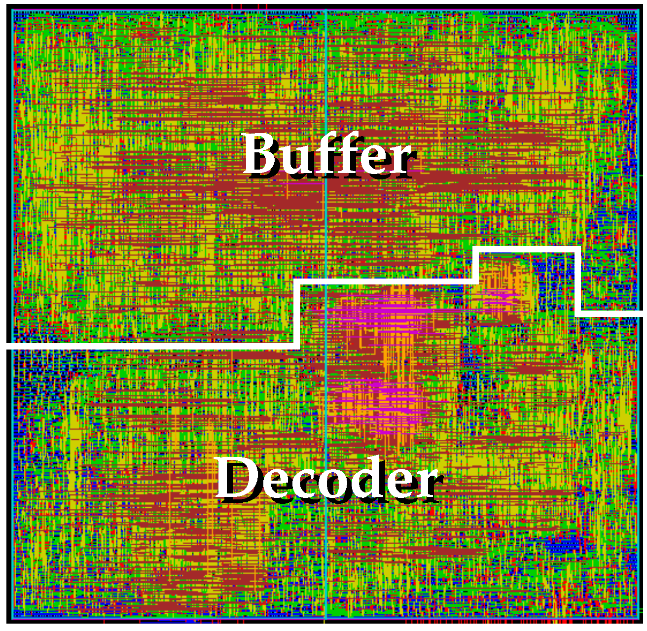
LCC, Q5 and Q6 decoders were implemented on an eight-metal layer 90 nm CMOS standard-cell technology with Cadence software and also in a Xilinx Virtex-V and Virtex-7 ultrascale FPGA devices with ISE and Vivado software, respectively. The chip layout of the proposed
LCC decoder in ASIC is shown in
Figure 7.
In
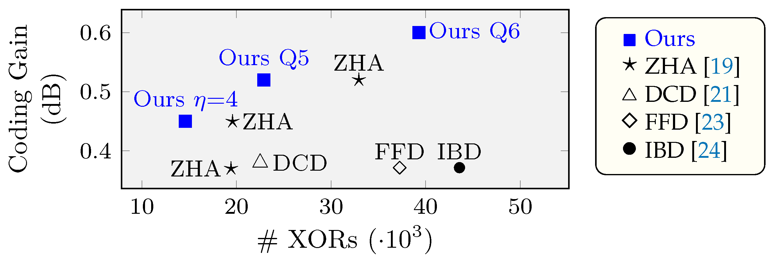
Figure 8, we compare the gate count (#XORs) and coding gain of the proposed decoders with the results from state-of-the-art soft-decision RS(255,239) decoders, specifically
LCC based on HDD (ZHA) [
19], Factorization-Free decoder (FFD) [
23] and Interpolation-Based decoder (IBD) [
24]. As can be seen, our decoders improve the ratio coding gain versus area, when compared with other decoders.
Table 1 shows the detailed gate count in ASIC (given in number of XORs) of the different blocks of the three proposed decoders.
Table 2 and
Table 3 compare, for the same RS code, our proposals and state-of-the-art published decoders, for ASIC and FPGA devices, respectively. On the one hand,
Table 2 compares our decoders with [
21], the only decoder, to the best of our knowledge, that provides complete implementation results in ASIC, and also with [
20]. On the other hand,
Table 3 compares our decoders with [
20], the only decoder, to the best of our knowledge, that provides complete implementation results in a Virtex-V FPGA device. As can be seen in
Table 2, our
LCC decoder requires 41% fewer gates in ASIC than [
21], whereas it has a 0.07 dB improvement in coding gain at FER =
compared to this decoder. Furthermore, our Q5 decoder has a gate count similar to [
21], but has 0.14 dB advantage in coding gain at FER =
. On the other hand, the comparison with [
20] is not that straightforward, due to differences in the technology used and the lack of gate count. Nevertheless, the reduction in area is clear when using the same Virtex-V FPGA device. As shown in
Table 3, in this case, our
LCC decoder reduces the LUT count in [
20] about 29 %. Moreover, Ref. [
20] has lower coding gain, since this is a
LCC decoder. Our decoder
LCC has similar area to the
LCC decoder in [
19], but it should be noted that [
19] does not include the multiplicity assignment stage.
In regard to latency and throughput results, as can be seen in
Table 2 and
Table 3, our decoders reach 450 MHz thanks to the low critical path, which is T
+ T
+ T
. The throughput of our
LCC and Q5 decoders in ASICs is
Gb/s. Since the decoder from [
21] has longer critical path and higher computational latency than our decoders (259 versus 256 cycles), the potential throughput that it can achieve is slightly lower than ours. On the other hand, since the decoders from [
19,
20] have the same critical path as ours but slightly higher computational latency than ours (275 versus 256 cycles), it is expected that our throughput is slightly higher: 1.3 Gb
versus 1.0 Gb
[
20], for the same FPGA device, as can be seen in
Table 3. Additionally, the proposed decoders have a latency of 546 cycles, whereas the DCD [
21] requires 777 cycles and the decoders from [
19,
20] require 550 clock cycles plus the pipeline.
Table 2 also shows chip area and consumption details for the proposed decoders. Our consumption data are obtained with the Static Power Analysis tool of the Encounter software from Cadence. It should be noted that the proposed decoders are implemented with different Standard-Cell libraries, number of metal layers and supply voltage compared to [
21]. For comparison purposes, we also implemented an
LCC decoder optimized for area and working at 320 MHz (the same clock frequency as the decoder in [
21]). For that implementation, the chip area is 0.268 mm
and the estimated power consumption is 21.3 mW, which are similar to those of the decoder in [
21].
More up-to-date FPGA device implementation results are shown in
Table 4. As can be seen, in this technology our decoders reach 2.5 Gb/s.
It should be noted that in the comparison with state-of-the-art decoders, the coding gain performance of other decoders [
19,
20,
21] is that of an
LCC decoder. The decoders we propose are the first ones that use 16 or more test vectors with their full-decoding capabilities. Zhang et al. [
19] give estimation results for
and
using their architecture: 19,594 and 32,950 XOR gates, respectively. The hardware requirement of the decoder is reduced to 14,643/19,594 = 75% and 22,947/32,950 = 70%, respectively. On the one hand, it should be noted that their estimation does not include the Multiplicity Assignment nor the Symbol Modificaction stages. On the other hand, these authors estimate the cost of the
LCC decoder assuming that the design of this decoder only requires the parallelization of specific resources (i.e., syndrome update, Key Equation Solver and polynomial evaluation), but, in the case of
and
, the use of a Gray code sequence in the decoding process is not straightforward. We propose a solution for this issue in the present work. Moreover, when a decoder has to process 32 or 64 test vectors by using 2 or 4 processing units in parallel, respectively, part of these units would have to process their last test vector while the processing of the next frame has already started (see
Figure 3). Processing those last test vectors would imply that the latency of the decoder increases and that a considerable amount of registers are required to concurrently process data from two frames. In the present work we propose a solution for this problem that still profits from the use of a Gray code processing sequence.


