Article

All SiC Grid-Connected PV Supply with HF Link MPPT Converter: System Design Methodology and Development of a 20 kHz, 25 kVA Prototype

1
Department of Electrical and Electronics Engineering, Hacettepe University, Beytepe, Ankara 06800, Turkey
2
Department of Electrical and Electronics Engineering, Middle East Technical University, Ankara 06800, Turkey
*
Author to whom correspondence should be addressed.
Electronics 2018, 7(6), 85; https://doi.org/10.3390/electronics7060085
Submission received: 7 May 2018 / Revised: 23 May 2018 / Accepted: 28 May 2018 / Published: 31 May 2018
(This article belongs to the Special Issue Applications of Power Electronics)

Abstract

:
Design methodology and implementation of an all SiC power semiconductor-based, grid-connected multi-string photovoltaic (PV) supply with an isolated high frequency (HF) link maximum power point tracker (MPPT) have been described. This system configuration makes possible the use of a simple and reliable two-level voltage source inverter (VSI) topology for grid connection, owing to the galvanic isolation provided by the HF transformer. This topology provides a viable alternative to the commonly used non-isolated PV supplies equipped with Si-based boost MPPT converters cascaded with relatively more complex inverter topologies, at competitive efficiency figures and a higher power density. A 20 kHz, 25 kVA prototype system was designed based on the dynamic model of the multi-string PV panels obtained from field tests. Design parameters such as input DC link capacitance, switching frequencies of MPPT converter and voltage source inverter, size and performance of HF transformer with nanocrystalline core, DC link voltage, and LCL filter of the VSI were optimized in view of the site dependent parameters such as the variation ranges of solar insolation, module surface temperature, and grid voltage. A modified synchronous reference frame control was implemented in the VSI by applying the grid voltage feedforward to the reference voltages in abc axes directly, so that zero-sequence components of grid voltages are taken into account in the case of an unbalanced grid. The system was implemented and the proposed design methodology verified satisfactorily in the field on a roof-mounted 23.7 kW multi-string PV system.

1. Introduction

Various grid-connected photovoltaic system concepts and topologies have been summarized previously [1,2,3,4]: (i) micro inverters [5,6]; (ii) residential systems supplied from a PV string [7,8]; (iii) commercial/residential systems supplied from multiple PV strings having their own maximum power point tracking (MPPT) converters and a central inverter [9,10]; and (iv) commercial/utility-scale PV plants supplied from a common DC link with a central inverter [11]. The central inverter in [11] performs direct conversion of PV power to AC from multiple PV strings. MPPT and reliable and efficient conversion of PV power to AC at grid frequency are the major design issues for two stage grid-connected PV systems [12]. In the PV systems performing direct conversion of PV power to AC, the voltage of the common DC link is varied by the central inverter against the changes in solar insolation and panel temperature [13]. An MPPT algorithm integrated into a two-layer controller is recommended in [14] for direct conversion of PV power through a three-phase grid-connected VSI. A neural network based MPPT algorithm is proposed in [15] to improve the dynamic performance of DC capacitor voltage at the input of VSI and to maintain faster tracking response against sudden changes in solar irradiance. Grid-connected PV supplies can be classified into two groups: (i) those having transformerless inverter topologies [16]; and (ii) those having magnetic transformers usually on the grid side [17]. Transformerless PV supplies require more complex and expensive inverter topologies as compared to PV supplies having transformers for galvanic isolation to prevent the flow of common-mode currents [18,19,20,21,22].
In the vast majority of commercially available PV supplies, new generation hybrid IGBTs are currently employed to synthesize grid frequency voltages and/or currents. In the next generation PV inverters, simpler circuit designs such as two-level instead of multi-level inverters are expected to be used for fewer components and hence higher reliability [23]. Wide bandgap (WBG) devices such as SiC power MOSFETs will be employed for higher switching frequency to reduce the size of passive components, heatsinks and hence the volume of the PV supply, as foreseen in [23]. WBG semiconductors show superior material properties, enabling potential power device operation at higher temperatures, voltages, and switching speeds than current Si technology [24].
In recent years, performances of all SiC PV supplies consisting of DC/DC converters and three-phase grid-connected inverters are assessed, as reported in [25,26,27]. These use either three-level T-type inverter topology [26] or cascaded multi-level inverter topology [27]. All SiC inverters such as single-phase H-bridge converter [28], neutral point clamped (NPC) T-type three-phase inverter [29], and three-phase five-level T-type inverter [30] are used to perform direct conversion of PV power to the grid. Design and performances of some non-application-specific two-level three-phase SiC inverters are presented in [31,32,33,34].
Since the power converters in PV supplies are presently switched at relatively higher frequencies, ranging from a few kHz to a few tens of kHz, sizing and design of these converters require the dynamic model of the PV cells, modules or arrays instead of the well-known static model. Some attempts have been made to obtain dynamic model parameters of various types of PV cells or modules by theoretical calculations and/or measurements [35,36,37,38,39,40]. The use of internal solar cell diffusion capacitance to replace the input capacitor in boost derived DC-DC converters has been proposed in [41] for energy harvesting applications. In almost all of the two-stage PV supplies, boost type DC-DC converters have been used for MPPT. Recently, in this area, small size SiC MOSFET [42,43,44,45] and SiC JFET based [46] MPPT converters are reported in the literature. A 1-MW solar power inverter with boost converter using all SiC power modules has been presented in [47]. A 3.5 kW, 100 kHz all SiC buck/boost interleaved MPPT converter is proposed in [48] for higher conversion efficiency. Design, construction, and testing of a general purpose 750-V, 100-kW, 20-kHz bidirectional dual active bridge DC–DC converter using all SiC dual modules with HF transformer is described in [49] to provide maximum conversion efficiency from the DC-input to the DC-output terminals.
Design of the AC filter on the grid side of a VSI is a compromise between performance and size. A step-by-step design procedure of an LCL filter for a grid-connected three-phase PWM voltage source converter is proposed in [50]. A new design method is recommended in [51] for LCL and LLCL filters with passive damping to be used in single-phase grid-connected VSIs. Peña-Alzola et al. [52] examined passive damping losses in LCL filters. Design methodology, analysis and performance of LCL filters for three-phase grid-connected inverters are also described in [53,54]. Stability regions of active damping control for LCL filters are discussed in [55]. A generalized LCL filter design algorithm for grid-connected VSIs is presented in [56].
The common control methods for three-phase grid-connected inverters are: (i) synchronous reference frame control (in dq-axes) [57,58,59]; (ii) stationary reference frame control (in αβ-axes) [60]; and (iii) natural reference frame control (in abc-axes) [61]. The main drawback of the synchronous reference frame control is the poor compensation capability of the low-order harmonics in the case of PI based controllers [60]. To cope with this drawback, the control system can be equipped with proportional resonant harmonic compensators, one pair for each prominent low order sidekick harmonics produced by the system itself [62]. In stationary reference frame control method, two proportional resonant controllers can be used in αβ-axes for the fundamental component to eliminate possible steady-state error which may arise in PI control. However, the number of PR controllers for low-order harmonic compensation are doubled. In abc control strategy, an individual controller is required for each line current on the grid side. In this control method, all types of controllers such as PI controller, PR controller, hysteresis controller, dead-beat controller and repetitive controller can be adopted [61].
This paper recommends a grid-connected, all SiC Power MOSFET based multi-string PV supply with a HF link MPPT converter in each string and a two-level central inverter. The design methodology described in the paper utilizes a custom dynamic model of the roof-mounted multi-string PV system, and site dependent parameters. These parameters are variation ranges of solar insolation, module surface temperature, and grid voltage. In the design procedure the following are optimized: (i) input DC link capacitance; (ii) switching frequencies of MPPT converter and VSI; (iii) the size and performance of HF transformer with nanocrystalline core; (iv) the DC link voltage; and (v) the LCL filter of VSI. Corresponding field test results of the implemented 20 kHz, 25 kVA prototype are presented. It has been shown that the HF link converter in cascade with a two-level VSI provides a viable alternative to multi-string PV supplies with a competitive efficiency, lower harmonic distortion and a much higher power density. This PV supply topology with a HF link MPPT converter makes possible the use of a simple and reliable, two-level, voltage source PV inverter for grid connection. In the case of PV supplies with non-isolated MPPT converters or those performing direct conversion of PV power to the grid, either complex inverter topologies or bulky grid-side common-mode filters or coupling transformers would be required to minimize the flow of undesirable common-mode currents.

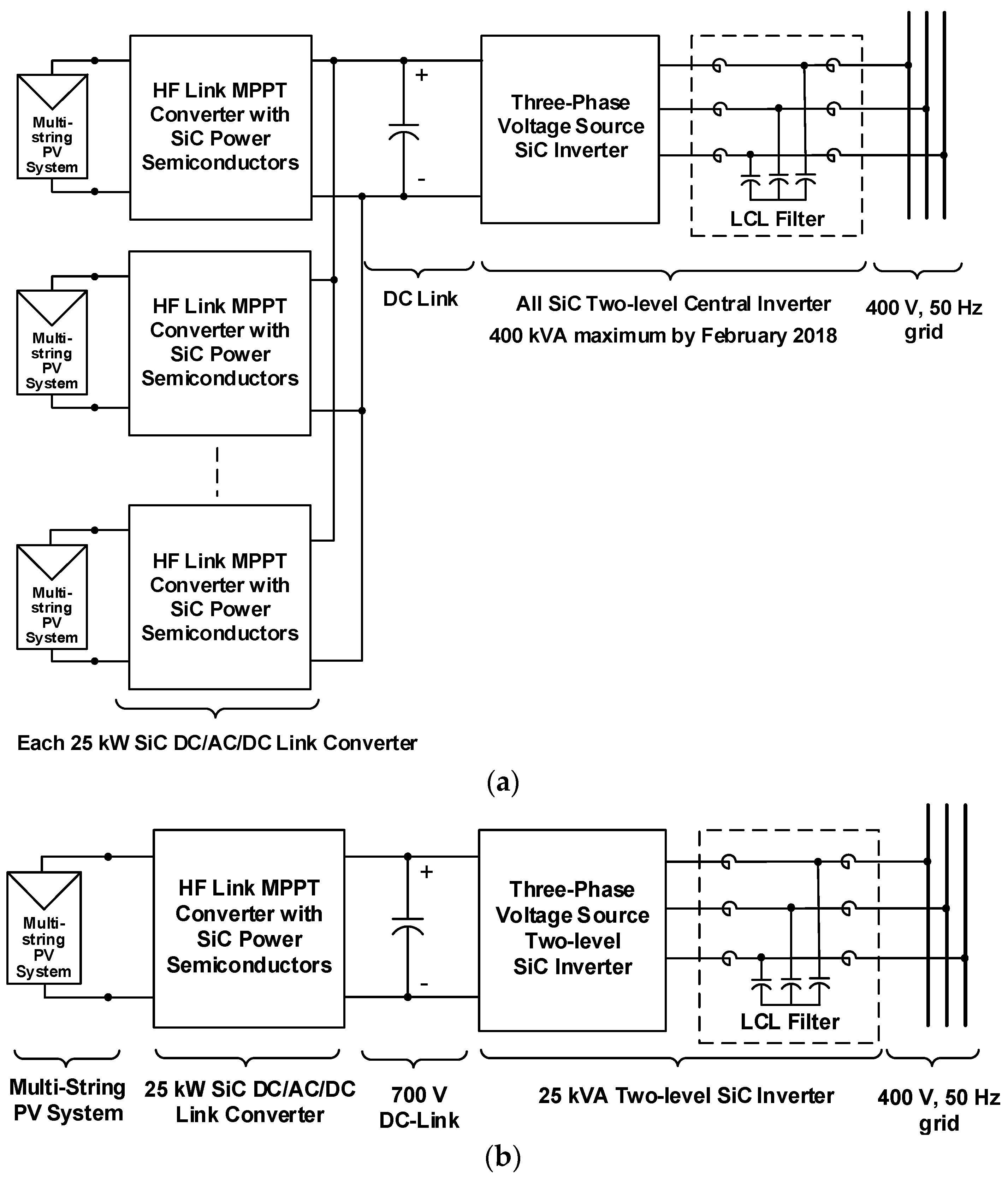
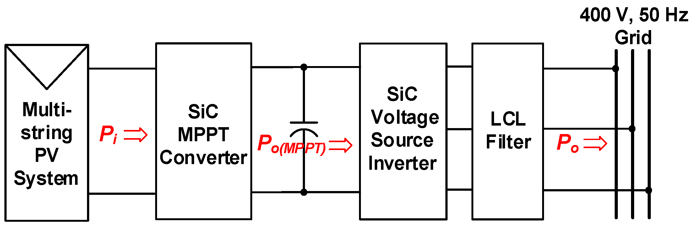
2. System Description

2.1. General

Block diagram representation of all SiC grid-connected PV supply with HF link is as shown in Figure 1a. With the advents in SiC power MOSFETs, the kVA rating of three-phase, two-level voltage source all SiC central inverter can reach 175–400 kVA, by employing commercially available three half-bridge all SiC modules in Table 1 (by February 2018) for direct connection to 400 V l-to-l, 50 Hz utility grid. Each MPPT converter with DC/AC/DC link can be designed to process 15–25 kW PV power by employing SiC half-bridge modules, TO-package SiC Schottky diodes, and a nanocrystalline transformer core. The MPPT converter rating in the application described in this paper is limited to 25 kW by considering the partial shading risk of multi-string PV panels. In the experimental system, five mono-crystalline PV strings of 23.7 kW peak under standard test conditions, with adjustable tilt angles occupy nearly 375 m2 in the roof area as shown in Figure 2. In this study, the experimental work was carried out on the prototype system given in Figure 1b.
Advantages and disadvantages of the multi-string PV supply system in Figure 1a can be summarized as follows:
(i)
In medium power applications, as a wide bandgap device, SiC power MOSFETs can be switched at higher frequencies (a few tens of kHz) in comparison with Si IGBTs. This ability brings us the following benefits:
  • Higher efficiency at the same switching frequency;
  • Much smaller HF transformer in DC/AC/DC link of the MPPT converter;
  • Much smaller electrolytic or metal film DC link capacitor at the output of the MPPT converter;
  • Much smaller distributed metal film DC link capacitor bank in the laminated bus/PCB of the inverter circuit;
  • Smaller LCL filter bank at the output of the PV inverter;
  • Silent operation;
  • Permits the use of two-level three-phase bridge inverter topology to conform with the power quality regulations on the grid side; and
  • Extends the range of high order current harmonics that can be eliminated.
(ii)
They eliminate the need for a bulky, grid-side PV transformer to provide electrical isolation.
(iii)
Separation of installed PV panels into multiple strings having MPPT converters minimizes the undesirable effects of partial shading.
(iv)
The central inverter has higher efficiency and lower cost in comparison with the usage of several smaller scale inverters.
(v)
In most countries, the PV system in Figure 1a can be directly connected to the low-voltage (LV) side of distribution transformers without the permission of distribution system operators. Although standard power ratings for distribution transformers are 100, 250, 400, and 630 kVA [67], higher ratings up to 2 MVA are also in service.
(vi)
Since the HF link MPPT converter is cascaded with the grid-connected PV inverter, overall efficiency is 1–2% lower than that of PV converters performing direct conversion of PV power to the grid. However, the PV systems having non-isolated MPPT converters or performing direct conversion of PV power to the grid should have more complex converter topologies to minimize common-mode currents.

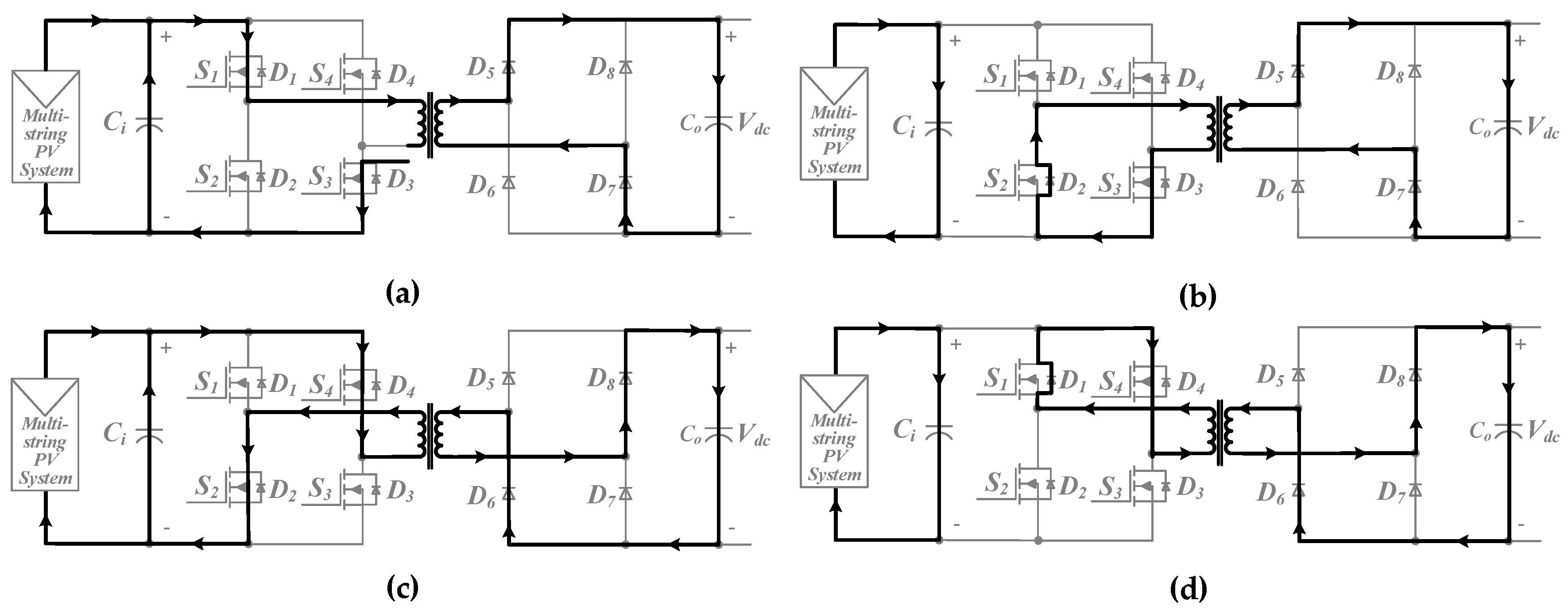
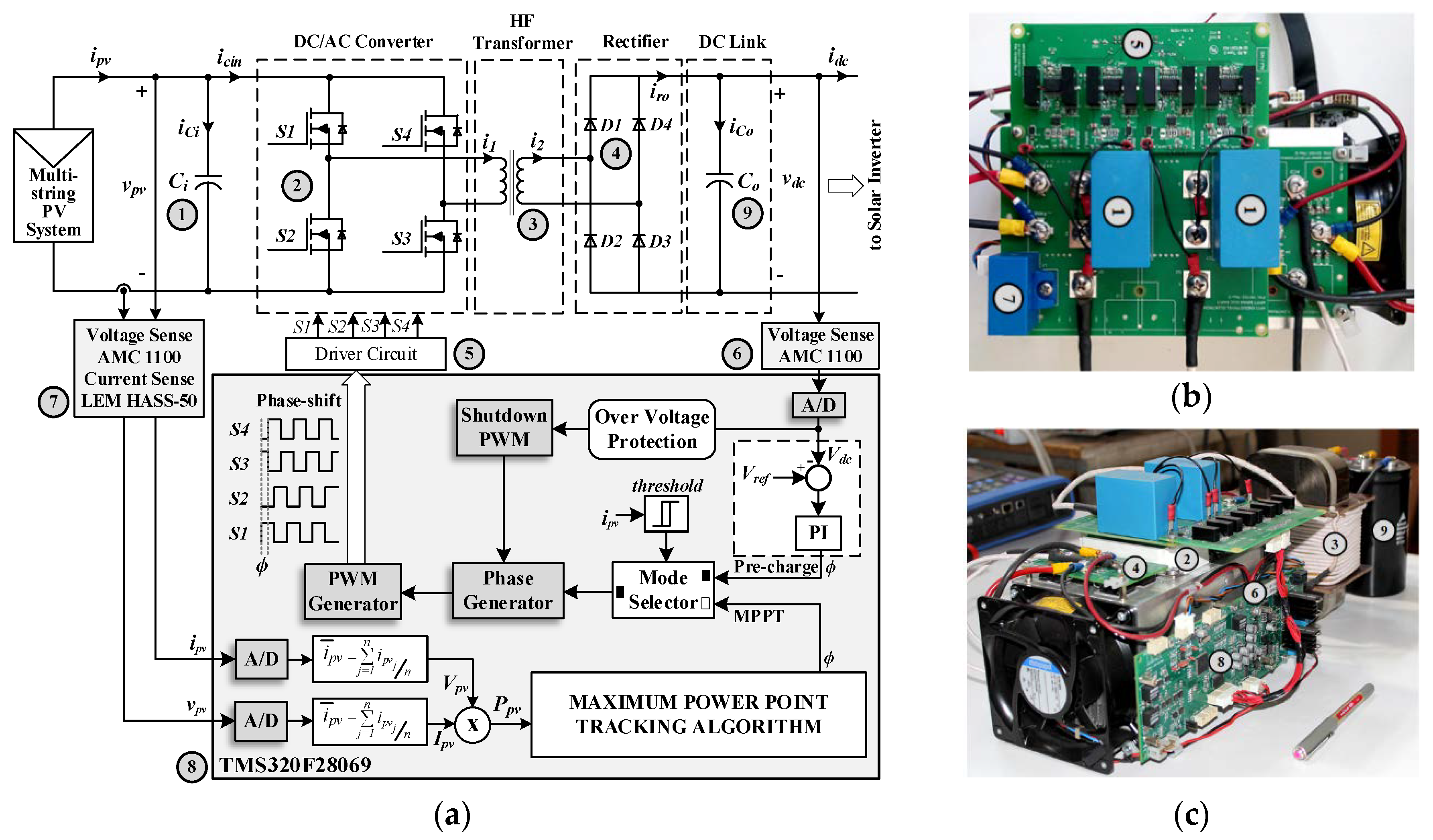
2.2. MPPT Converter with HF Link

A prototype of the MPPT converter with HF link shown in Figure 1b is designed and implemented. MPPT converter is composed of a SiC Power MOSFET based single-phase H-bridge converter, a HF transformer, and a SiC Schottky diode rectifier. The circuit diagram of the power stage, the control circuitry, and top and side views of the implemented MPPT converter prototype are as shown in Figure 3.

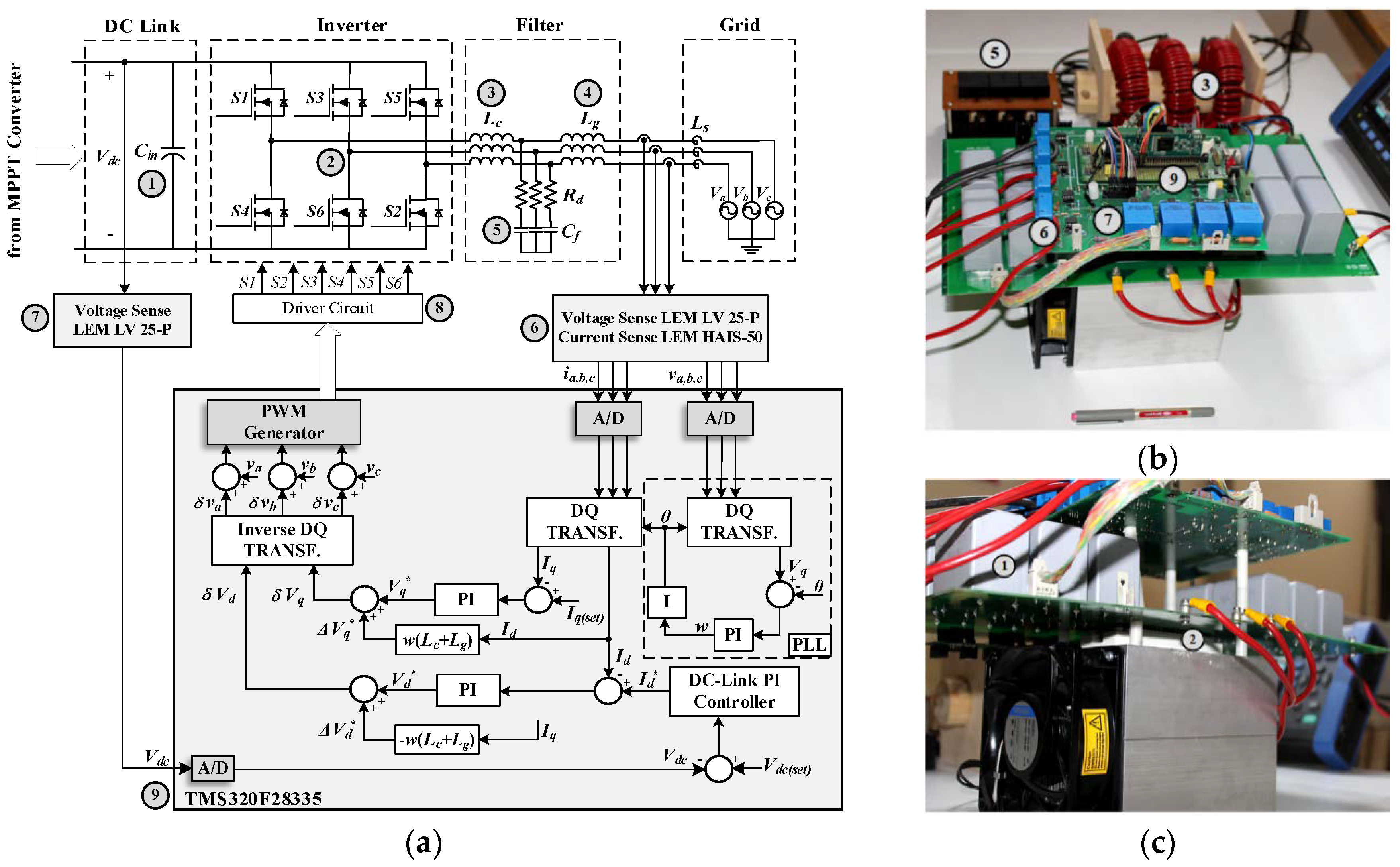
2.3. Three-Phase Two-Level Voltage Source Inverter

A prototype of the three-phase two-level voltage source inverter shown in Figure 1b was designed and implemented. This converter topology was chosen for the following reasons:
  • The ability of SiC power MOSFETs at high switching frequencies for lower harmonic current content;
  • Minimum power semiconductor count gives higher reliability in comparison with multi-level converters;
  • Common-mode current is not a design concern because of the HF transformer in the MPPT converter; and
  • PV inverter delivers power to one of the most common low voltage utility grid.
The circuit diagram of the power stage and its control circuitry, and top and side views of the implemented inverter prototype are shown in Figure 4.

3. Modeling and System Design

The recommended modeling and system design methodology is described in this section for the existing multi-string PV system shown in Figure 2. For another multi-string PV system configuration, the same design principles can be applied.

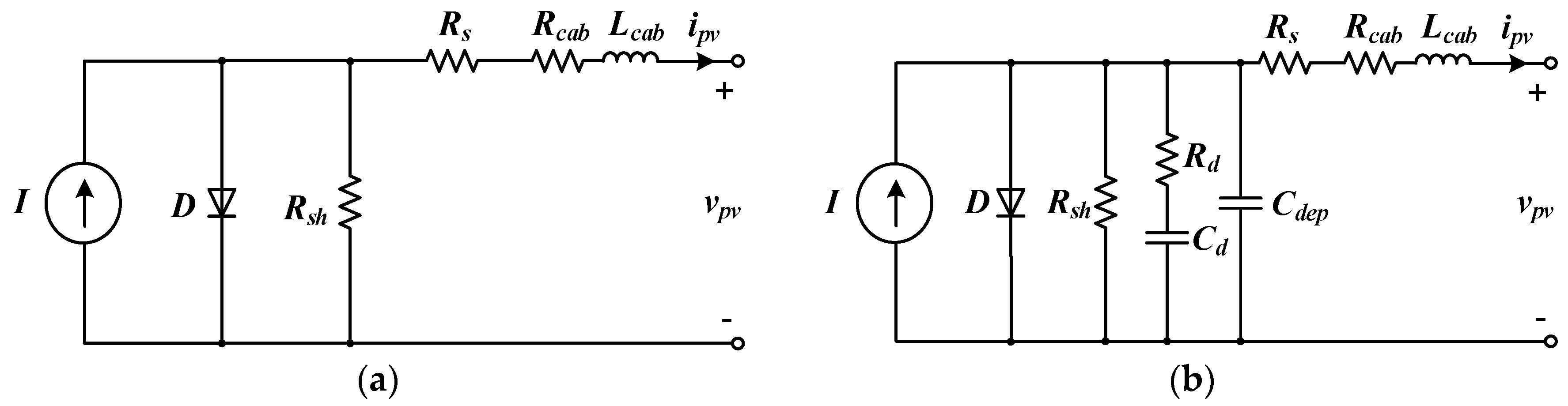
3.1. Dynamic Model of Multi-String PV System

Even in the steady-state operation of PV supplies, their power converters such as the MPPT converter and the inverter operate in the periodic transient state, instead of pure DC operation. Therefore, in the analysis and design of such systems, a proper dynamic model of the multi-string PV system is to be used. Several attempts have been made to obtain dynamic models of a PV module [35,36,37,38,39,40,41]. However, in this research work, the dynamic model parameters of the roof-mounted multi-string PV system shown in Figure 2 were obtained from a set of experimental data. It includes also all cabling and wirings up to the input terminals of the MPPT converter. These parameters were then combined with the static model of the CSUN250-72M modules available in MATLAB/Simscape/Power Systems R2016b for use in the design work.
Equivalent circuits of the multi-string PV system in Figure 2 consisting of 95 pieces of CSUN250-72M modules (5 × 19 modules) are as shown in Figure 5. Static model in Figure 5a is determined for the PV array in Figure 2 by using the PV array block developed by the National Renewable Energy Laboratory (NREL) System Advisor Model and available in MATLAB/Simscape/Power Systems R2016b. However, the design of the PV supply presented in this paper is based on the dynamic model of the PV system shown in Figure 5b.
The topology of this dynamic model is nearly the same as the one given in [41]. The dynamic model parameters are estimated from the results of two tests conducted on the multi-string PV system. In the first test, multi-string PV system is solidly short-circuited at the terminal box and the short-circuit current is recorded as shown in Figure 6a. In the second test, a slightly inductive resistive bank is suddenly connected to the open-circuited multi-string PV system terminals and the terminal voltage and the current are recorded as shown in Figure 6b. Parameters of the multi-string PV system estimated from the current and voltage records shown in Figure 6 are as given in the caption of Figure 5.
These experimental records are compared with the simulation results obtained by MATLAB/Simscape/Power Systems, for the static and dynamic models separately under the same test conditions, as given in Figure 6. It is clear from this figure that the dynamic model gives much better results than those of the static model, and it can therefore be satisfactorily used in the design of HF link MPPT converter.

3.2. Three-Phase Two-Level VSI

In this subsection, optimum DC link voltage and switching frequency are determined and the design of the inverter circuit, its control circuitry and LCL filter are described. The design of the HF link converter is directly affected by the optimum DC link voltage determined in this subsection.

3.2.1. Optimum DC Link Voltage

DC link voltage, Vdc, is kept constant by the inverter against the variations in PV power over the entire operating range of the PV supply. At the optimum value of Vdc, modulation index, M in Equation (1) of the inverter circuitry should vary in a range as close as possible to unity in order to minimize harmonic distortion of the output line currents.
M = ( 2 2 / 3 ) ( V / V d c )
where V is the l-to-l value of either grid voltage, Vs or consumers load voltage, Vt. Furthermore, in calculating the variation range of M, permissible changes in 400 V l-to-l, 50 Hz grid voltage are as specified in IEC 60038 2002-07 Standard Voltages [68]. This standard specifies the maximum changes in grid voltage, Vs as +6% to −0% while a further ±4% at the consumers load voltage, Vt. In view of these considerations, the variation ranges of M are calculated and plotted (Figure 7).
As can be understood from the results in Figure 7, the optimum value of Vdc is around 700 V. This choice may result in operation slightly in over-modulation region as given in Figure 7b. Since inverter rating is 25 kVA/22.3 kW for the available multi-string PV system, the inverter can deliver nearly 11 kVAr inductive or more to bring Vt back to Vs = 400 V + 6%. Application of third harmonic injection method [69,70] might be an alternative design approach in which the optimum value of Vdc is to be nearly 600 V for Vs = 400 V + 6%.

3.2.2. Optimum Switching Frequency

Higher switching frequencies for the two-level three-phase inverter with different modulation techniques such as SPWM, SVPWM, etc., excluding SHEM, result in low harmonic distortion for the line currents injected into the grid [71]. In this research work, sinusoidal PWM is chosen as the modulation technique because of its simplicity, and its ability to illustrate basic design guidelines. Since SiC Power MOSFETs can be switched at higher frequencies in comparison with Si IGBTs for the same power dissipation and solar inverter rating, power loss components of solar inverter with SPWM modulation are calculated for a reasonable operating frequency range, e.g., at fsw = 10, 20, and 30 kHz, by using the expressions and manufacturers’ design tools given in [72].
The associated pie-charts are shown in Figure 8. All wiring and cabling losses between discrete components, inverter, LCL filter, and grid are ignored in the preparation of Figure 8. In addition, extra power losses due to the switching ripple current through the power MOSFETs are not considered by the power loss calculation tools mentioned above in the calculation of conduction and switching losses. In summary, slightly higher loss content and a lower efficiency are expected for the solar inverter in the field tests.
In the design of LCL filter at different switching frequencies, only the converter side inductance, Lc, is optimized to keep its peak-to-peak current ripple constant at 25%. Power loss components in the associated LCL filters are then used in the preparation of pie charts in Figure 8. Although 10 kHz switching frequency reduces the power dissipation marginally in comparison with that of the 20 kHz, a considerably larger LCL filter size is to be used. Therefore, in the design and implementation of the solar inverter, fsw = 20 kHz is chosen, which is a compromise between losses and LCL filter size.

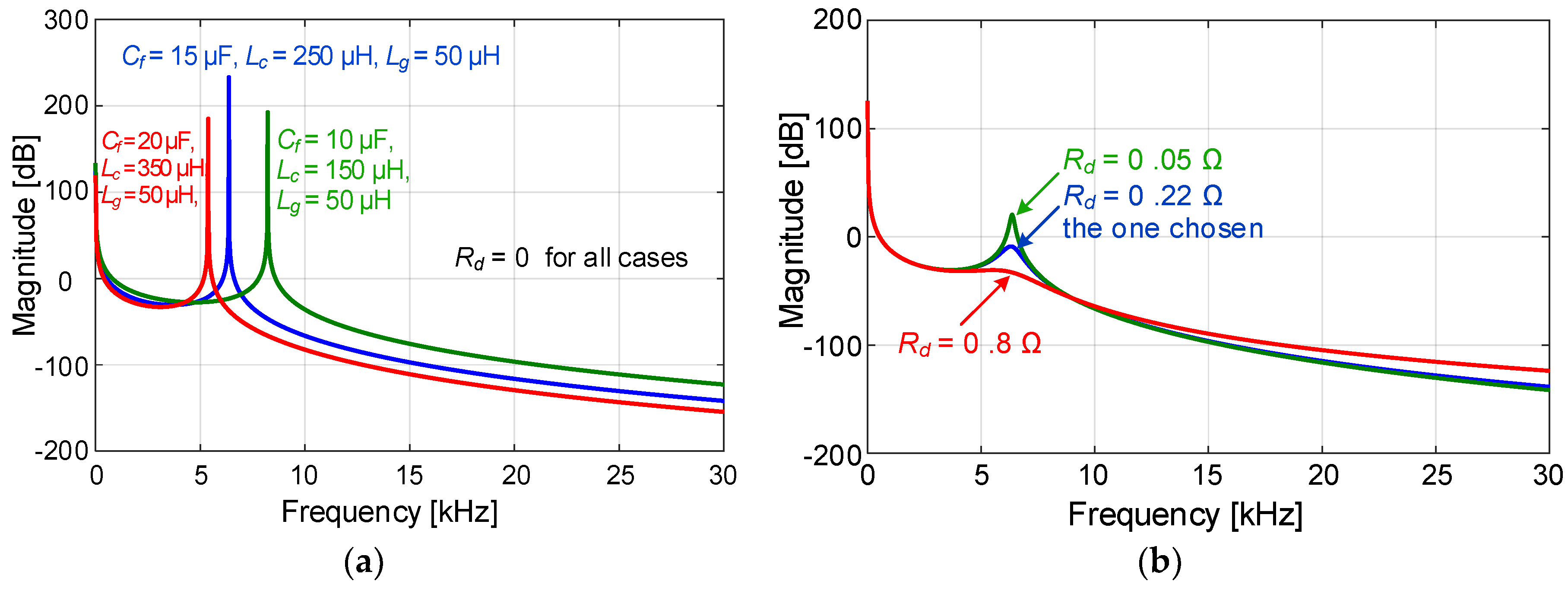
3.2.3. LCL Filter Design

An LCL filter consisting of inverter side inductors Lc, shunt capacitors Cf, passive damping resistors Rd, and grid side inductors Lg are considered in design, as shown in Figure 4a. The LCL filter should be designed to have not more than 10 A peak-to-peak ripple superimposed on 36 A rms fundamental current in Lc at 25 kVA, and 400 V l-to-l. Peak-to-peak ripple remains nearly constant over the entire operating range of the all SiC three-phase grid-connected two-level inverter and is 25% at 25 kVA, 400 V l-to-l. The corner frequency of the LCL filter is chosen around 1/3rd of the 20 kHz switching frequency. These choices are consistent with the recommendations given in various papers [50,51,52,53,54,55,56]. The transfer function Bode plots of undamped LCL filter for three different Lc, Cf, and Lg parameter sets are given in Figure 9a. All of them provide nearly 100 dB attenuation at switching frequency. Among these, Lc = 250 μH, Cf =15 μF, and Lg = 50 μH parameter set is chosen for the implementation. Red colored parameter set (Lc =350 μH, Cf =20 μF, Lg = 50 μH) is not chosen because its Lc is nearly 40% greater than that of the optimum design and provides unnecessarily high attenuation. Although the green colored parameter set (Lc = 150 μH, Cf = 10 μF, and Lg = 50 μH) gives minimum LCL size, it is also not chosen in the implementation because it makes narrower the control range of the phase shift angle, and hence may cause undesirable oscillations in the output power and possible instability. On the other hand, field experience has shown that larger LCL filter size reduces harmonic content of the line currents and maintains stability of the inverter.
Very high amplification of the current component at resonance frequency can be entirely eliminated by either passive or active damping technique. In this research work, passive damping is preferred and the damping resistance Rd is connected in series with Cf. In choosing the optimum value of Rd, a compromise is needed between copper losses and damping effect.
The effects of various damping resistors on the current transfer function bode plots of the chosen parameter set are as given in Figure 9b. Although lower Rd values are less dissipative, their damping effect is inadequate. On the other hand, higher Rd values provide strong damping at resonance frequency at the expense of higher losses and reduced attenuation at high frequencies. Rd = 0.22 Ω is therefore chosen for the implementation.

3.2.4. Controller Design

In this paper, active power delivered to the grid is controlled by using the rotating reference frame synchronized with the grid frequency by implementing a modified version of the control technique presented in [50]. The block diagram of the designed and implemented DSP (TMS320F28335) based controller is shown in Figure 4a. Line to neutral voltages va,b,c and line currents ia,b,c on the grid side, and DC link voltage Vdc are the inputs to the controller. These quantities are sampled at 10 kHz/channel. Set values of the DC link voltage, Vdc(set) and Iq(set) are adjusted, respectively, to 700 V and 0 A in the control software. PWM signals applied to the driver circuits are the outputs of the control system. Control actions are achieved firstly in rotating DQ reference frame which is synchronized with the grid frequency by the PLL circuit, and then in ABC reference frame.
To be able to lock to the grid, reference value of Vq should be 0. PI controller in the PLL circuit calculates synchronous speed, ω which is equal to angular frequency of the grid voltage. ω is then integrated to give space angle θ, where θ defines relative position of synchronously rotating reference frame with respect to the stationary ABC reference frame, i.e., relative position of rotating d-axis with respect to stationary a-axis. Iq is compared with Iq(set) = 0 for zero reactive power and then processed in the PI controller to generate reference signal Vq*. Cross-coupling term ΔVq* is then superimposed on Vq* to compensate for potential drop on the total filter inductance and also for better transient response in the feed-forward form of cross-coupling terms. Actual value of DC link voltage Vdc is compared with its set value Vdc(set) and resulting error signal is then processed in a PI controller to generate reference signal Id*. Id* is then compared with actual current Id and processed in a PI controller to generate reference value, Vd*. Cross-coupling term ΔVd* is superimposed on Vd* to compensate for potential drop on the total filter inductance and also for better transient response.
The above operations yield main control signals δVd and δVq in synchronously rotating reference frame. Instead of superimposing δVd and δVq on d- and q-axis components, Vd and Vq of the grid voltages, δVd and δVq are transformed back to abc-axes, resulting in δva, δvb, and δvc, and these control signals are then superimposed on the actual grid voltage waveforms va, vb, and vc. This modification results in lower harmonic distortion in the line current waveforms because when the actual grid voltages are transformed to dq reference frame (instead of dq0) and then used in the control together with δVd and δVq, odd multiples of third harmonic (zero sequence component) would not be taken into account.

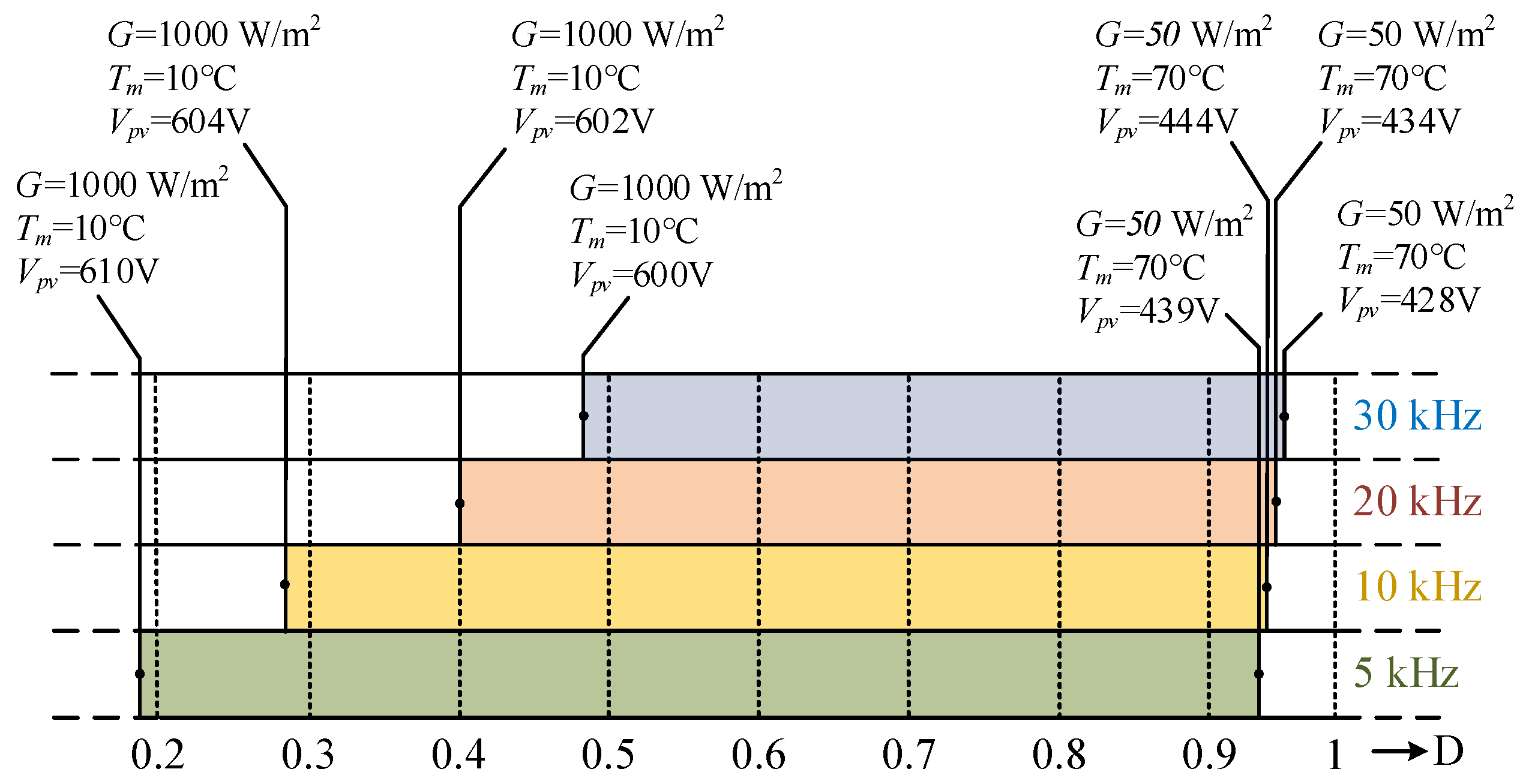
3.3. MPPT Converter with HF Link

In this subsection, switching frequency of the H-bridge converter and the transformer turns-ratio are optimized in view of the following design constraints:
(i)
Multi-string PV system and its dynamic model should be known. For this purpose, the system in Figure 2 and its dynamic model in Figure 5b are prespecified for the experimental set-up in Figure 1b.
(ii)
The variation range of global solar insolation, G, should be known for the geographical location at which the PV system is going to be installed, i.e., G ≤ 1000 W/m2 for the experimental set-up.
(iii)
The variation range of module surface temperature, Tm, should be estimated, i.e., 10 ≤ Tm ≤ 70 °C for the experimental set-up.
(iv)
DC link voltage, Vdc, is kept constant at 700 V by the solar inverter in the experimental set-up.
(v)
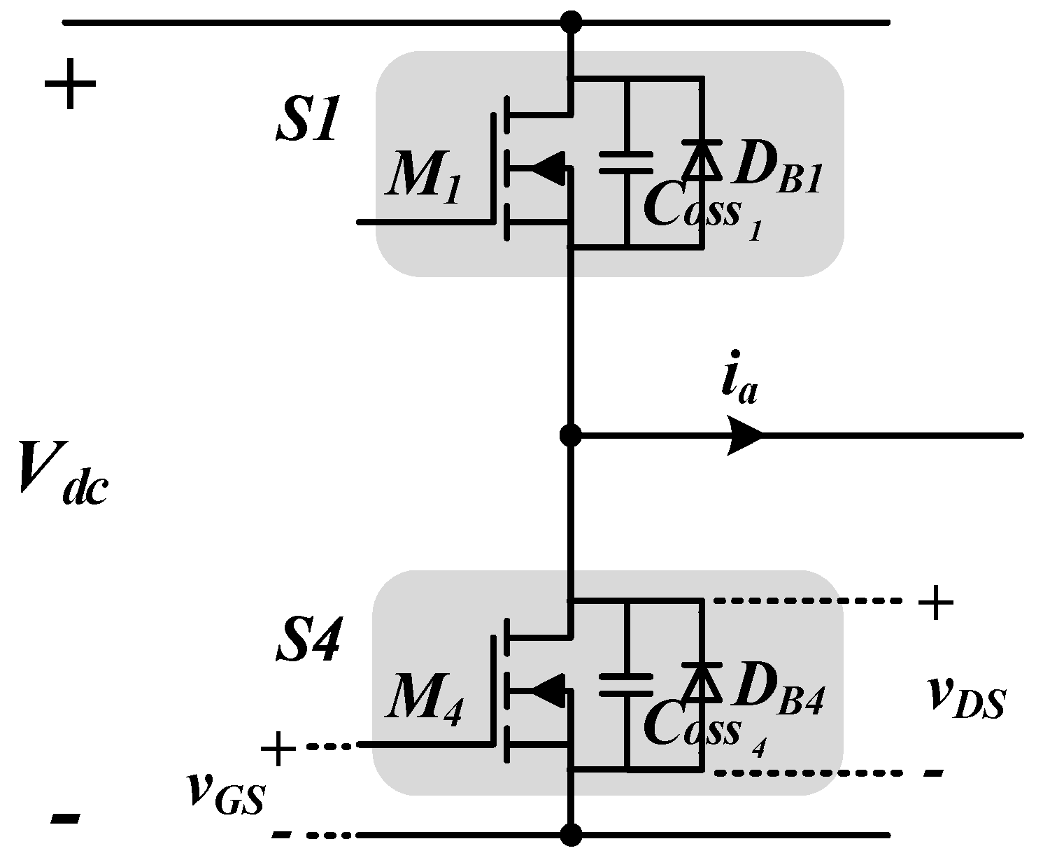
DC link capacitance, Co in Figure 3a is taken to be 3400 μF.
All calculations are carried out on MATLAB/Simscape/Power Systems by using the equivalent circuit in Figure 3a in which leakage inductances of the HF transformer are assumed to be Lp = 3.2 μH and Ls = 7.4 μH, respectively, on the primary and secondary sides, and switching losses of all SiC power MOSFETs and Schottky diodes are neglected.

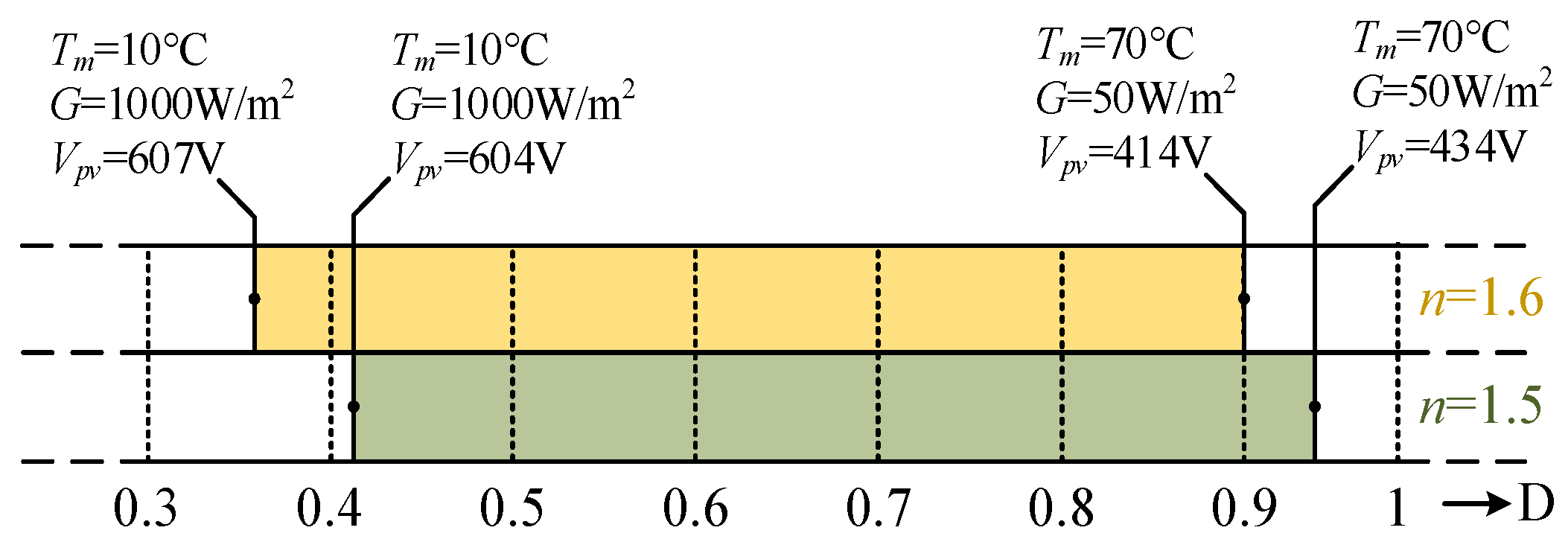
3.3.1. Optimum Transformer Turns-Ratio, n

The lowest and the highest maximum power point voltages for the multi-string PV system in Figure 2 are, respectively, Vmpp(min) = 434 V at G = 50 W/m2, Tm = 70 °C, and Vmpp(max) = 600 V at G = 1000 W/m2, Tm = 10 °C. Transformer turns-ratio is defined as n = Ns/Np, where Ns and Np are the number of series turns of the secondary and primary windings, respectively. The duty cycle, D, of the phase-shifted H-bridge converter is as defined in Equation (2).
D = ton/(ton + toff)
where ton is the power transfer period of phase-shifted H-bridge, and toff is the sum of freewheeling and no-conduction periods. It is desirable to maintain the operation of H-bridge converter at relatively high D values over the entire operating range to keep corresponding peak values of SiC power semiconductor and transformer currents relatively low. The variation ranges of D for two different n values and extreme operating conditions are shown in Figure 10.
On the other hand, for an ideal MPPT converter, the lowest MPPT voltage, Vmpp(min), over the entire operating range can be related to the chosen DC link voltage, Vdc = 700 V in terms of n and D as given in Equation (3). As an example, for D = 1.0 and Vmpp(min) = 434 V at G = 50 W/m2 and Tm = 70 °C, n is found to be 1.61 from Equation (3). However, an n value lower than 1.61 can be chosen, since the total leakage inductance of the transformer provides boosting action in a practical MPPT converter.
In the implemented MPPT converter, n = 1.52 is chosen for which D = 0.94 and Vmpp(min) = 434 V at G = 50 W/m2 and Tm = 70 °C. This choice ensures power transfer even at the minimum G and maximum Tm conditions and provides a margin for better transient response.
Vdc = 700 ≤ Vmpp(min) n D

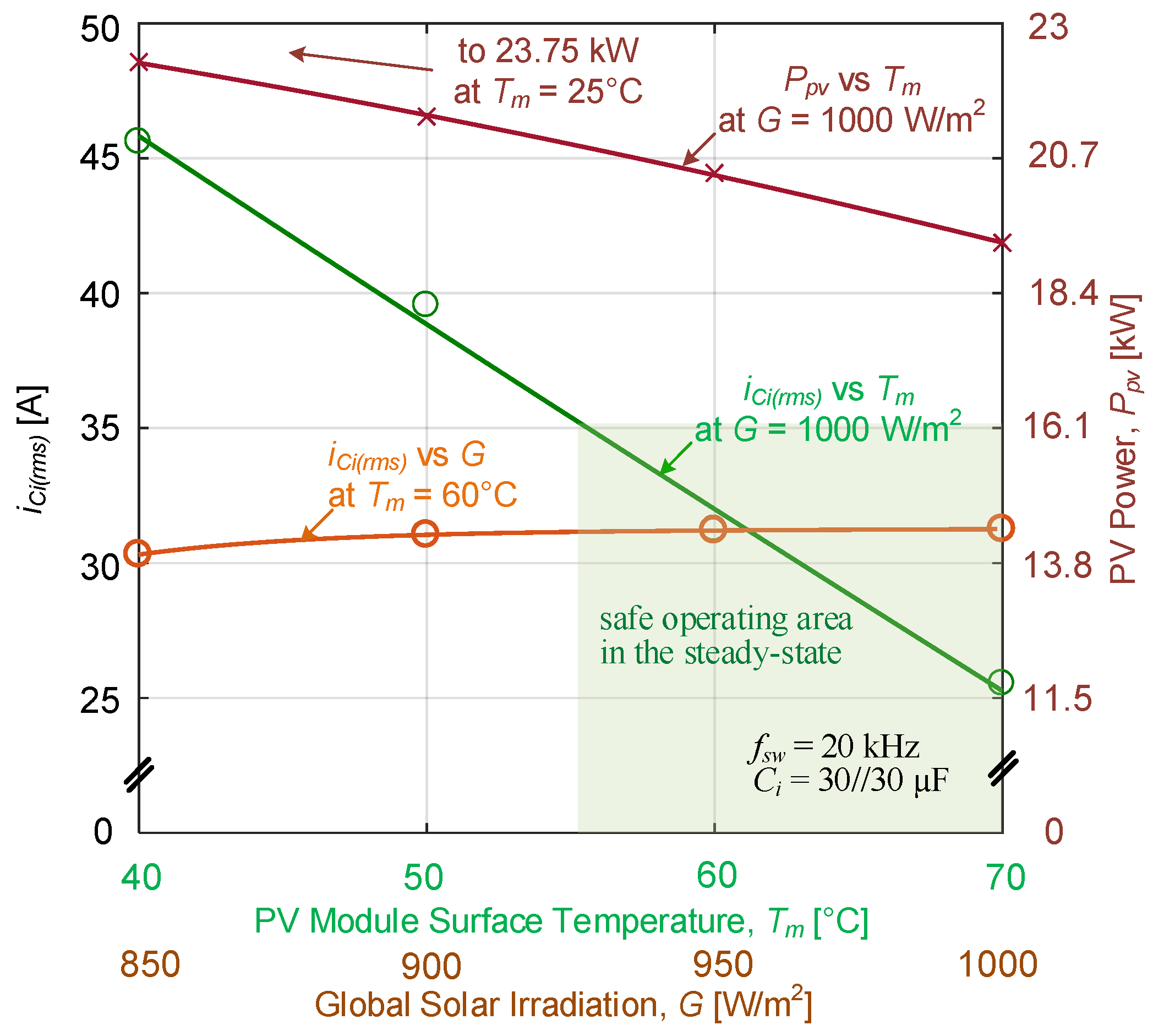
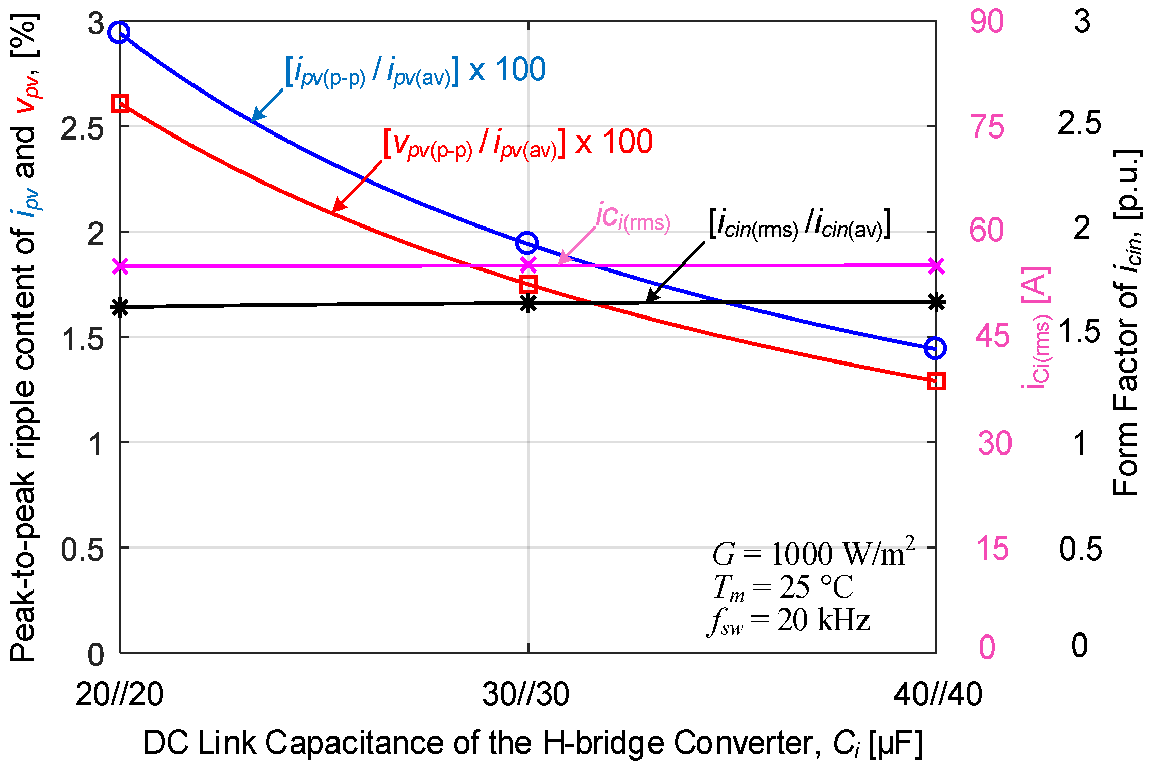
3.3.2. Choice of DC Link Capacitor of H-Bridge Converter

Operation modes of the MPPT converter in Figure 3 are as defined in Figure 11. The controllable section of the MPPT converter is the phase-shifted H-bridge converter. The stray inductance of the implemented DC-bus on PCB is estimated as Lstray = 15.2 nH. Two discrete metallized film capacitors are connected across the DC link, one for each leg of the H-bridge converter. Total DC link capacitance is denoted by Ci in Figure 3 and Figure 11. Suppose now that initially S1 and S3 are conducting in power transfer mode in the positive half-cycle as shown in Figure 11a.
When S1 is turned off, current is commutated to D2 which starts the freewheeling mode through S3 and D2 as shown in Figure 10b. The freewheeling mode is then followed by the OFF mode after the current decays to zero. For the negative half cycle, other diagonal switches S2 and S4 are turned on for power transfer mode which is followed by freewheeling mode through S4 and D1, respectively, shown in Figure 11c,d. Note that the converter is operated in the discontinuous conduction mode, owing to the absence of a lossy and bulky output filter inductor in the design.
Fall time of the SiC power MOSFET used in this research work is nearly 50 ns with increased gate resistance, Rg. During the commutation period, current closes its path mainly through Ci. The potential drop on Lstray is therefore Vstray = Lstray. (ΔIt) = 51 V for maximum possible device current of ID = 200 A at fsw = 20 kHz when G = 1000 W/m2, Tm = 10 °C on the predefined geographical site. Vstray will then be superimposed on drain-to-source voltage, vDS, of outgoing SiC power MOSFET. Since open-circuit voltage of the multi-string PV system is 800 V, peak value of vDS never exceeds 850 V in the worst case which is safely below the vDS rating of the chosen SiC power MOSFETs.
A high Ci value is always desirable for better system performance at the expense of higher size and hence cost. Simulation studies have shown that a Ci value in the range from 20//20 μF to 40//40 μF can be chosen in the implemented H-bridge converter. Effects of Ci on peak-to-peak ripple content of ipv and vpv, ici(rms), and form factor of icin are shown in Figure 12 for standard test conditions (G = 1000 W/m2, Tm = 25 °C) and fsw = 20 kHz. These curves show that:
  • ici(rms) and form factor of icin are not affected by Ci; and
  • Peak-to-peak ripple content of ipv and vpv reduces as Ci is increased. Lower peak-to-peak content on the PV side is always desirable, not only for potential drop on all series inductances but also for MPPT efficiency.
In view of these characteristics, Ci greater than or equal to 30//30 μF seems to be suitable for the implemented H-bridge converter, provided that the commercially available metallized film capacitors can carry this rms current. In the implemented system Ci = 30//30 μF is chosen which is bigger than the DC link capacitor recommended by the SiC power MOSFET manufacturer [73]. To justify that 30//30 μF meets the entire operating range of the MPPT converter for the predefined geographical location and their commercial availability, characteristics in Figure 13 and manufacturer’s data in Table 2 are given.

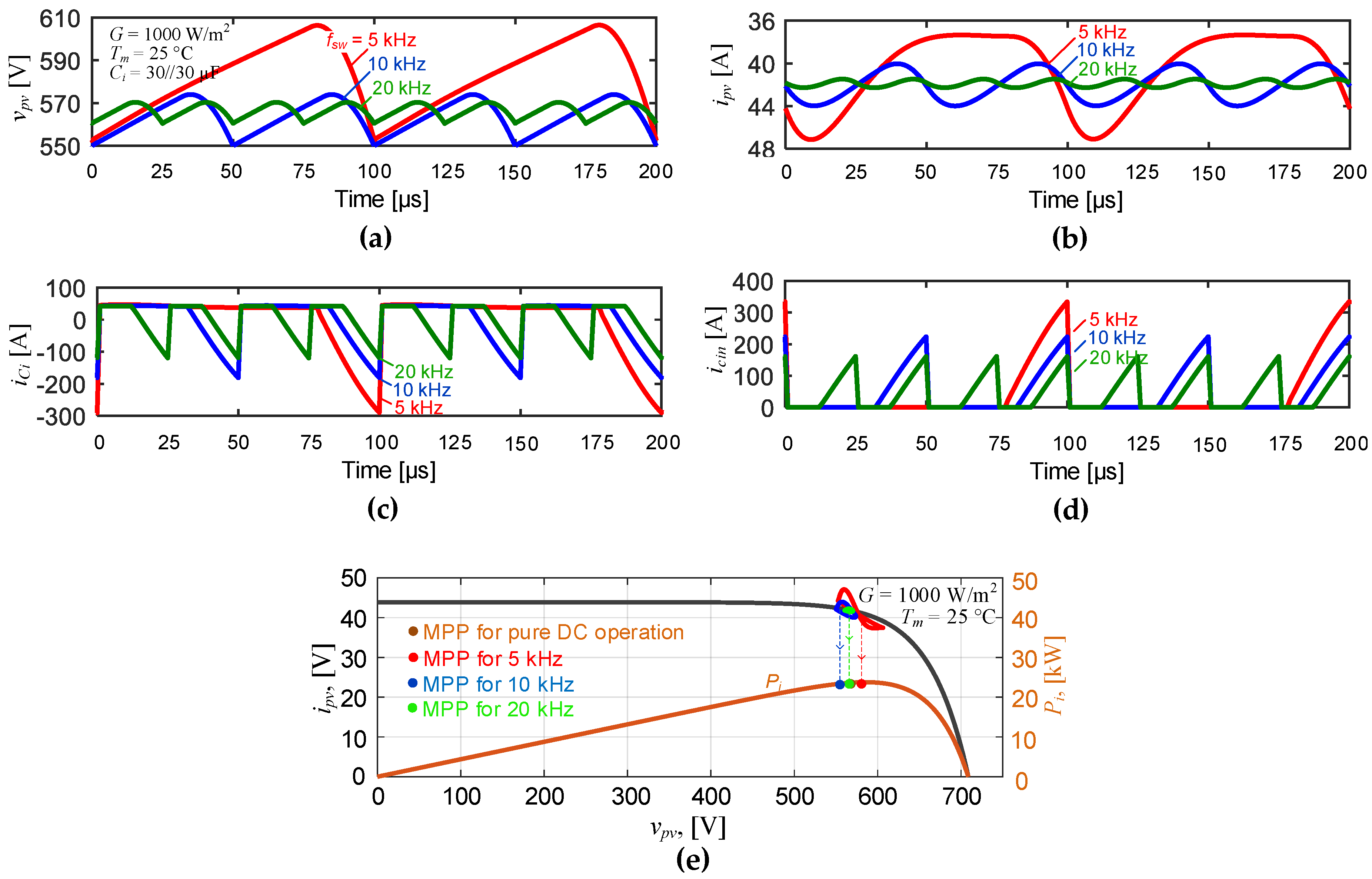
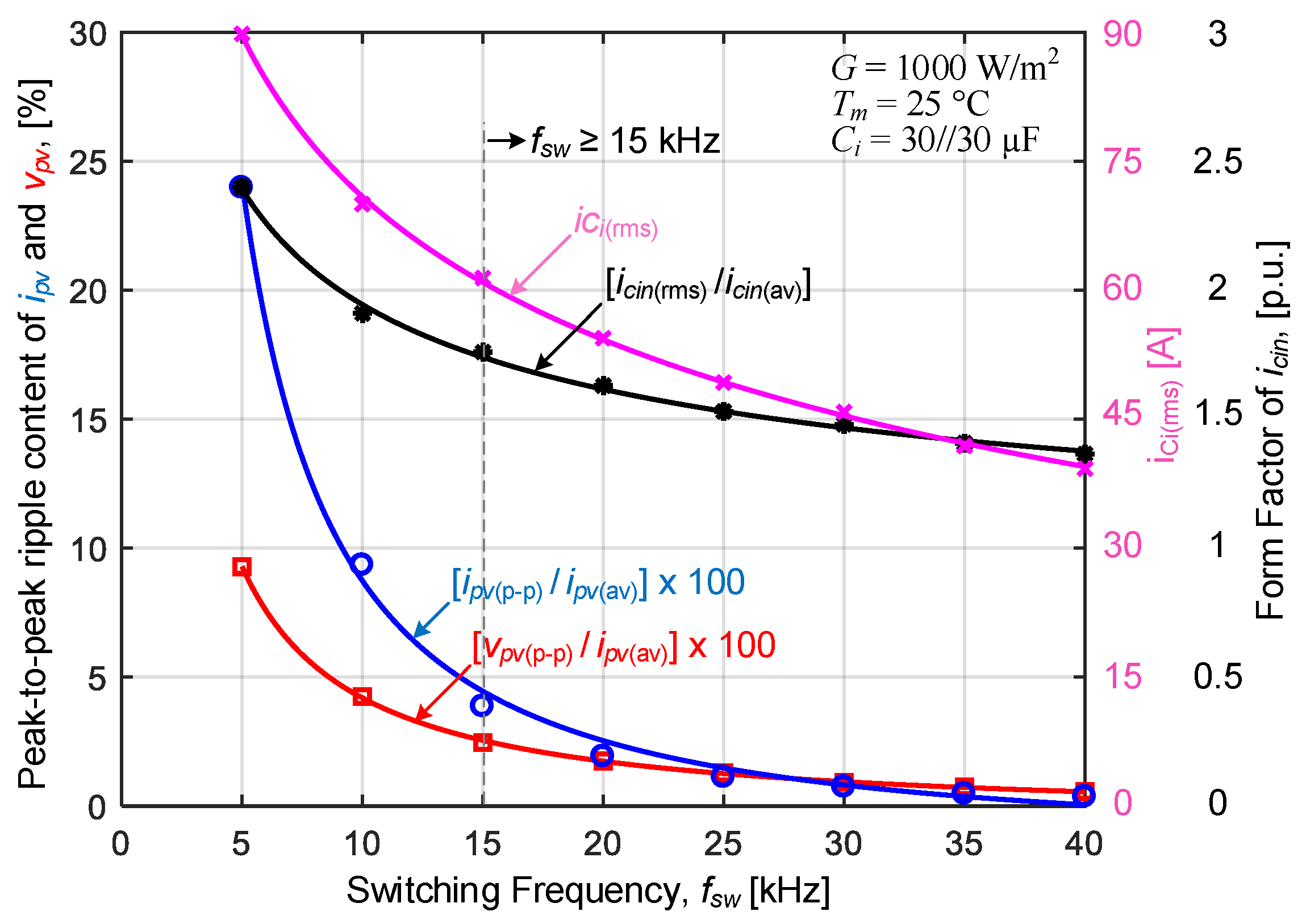
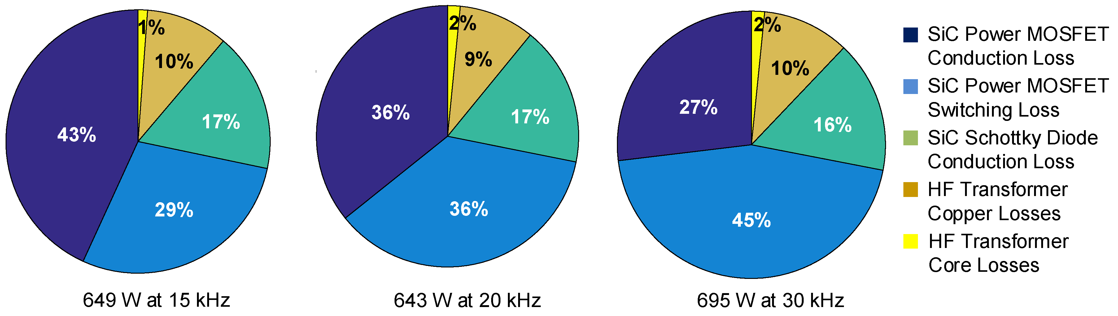
3.3.3. Optimum Switching Frequency of H-bridge Converter

Variations in ripple contents of vpv, ipv, iCi, and icin against switching frequency, fsw, obtained by simulation studies at standard test conditions for the chosen Ci = 30//30 μF are as given in Figure 14.
As can be understood from these waveforms, operation at higher switching frequency reduces ripple contents and hence rms values of all currents. Lower rms values for icin and iCi are better in the selection not only of SiC power MOSFET but also of DC link capacitor, Ci. These variations are quantified and presented in graphical form as a function of fsw in Figure 15. It can be concluded from these characteristics that the phase-shifted MPPT converter should be switched at a frequency greater than or equal to 15 kHz. Figure 14e justifies this statement. Dynamic variations in MPPs arising from ripple content of ipv are marked on ipv/vpv characteristic given in Figure 14e. Calculated mean MPPs are also marked on the same figure. The ideal case is pure DC operation. As fsw is increased dynamic MPP curve converges to that of pure DC operation, e.g., MPP power for fsw = 20 kHz is nearly the same with that of pure DC operation.
Thus far, in this subsection, only the factors for standard test conditions affecting the selection of fsw have been considered. However, the entire operating range of the MPPT converter installed at the predefined geographical site gives more valuable information about the selection of fsw. For this purpose, the variation range of duty ratio, D, for the H-bridge converter is calculated for different switching frequencies, and given in Figure 16. D should vary in a narrow range and at relatively high values to keep rms value of the semiconductor current, and hence its form factor at relatively low values. In view of these discussions, fsw of the H-bridge converter should be at least 20 kHz.
In the selection of fsw, the size of the HF transformer and the switching and conduction losses of H-bridge converter and conduction losses of Schottky diode rectifier should also be considered. Total semiconductor losses in the MPPT converter as a function of fsw are given in Table 3. These losses exclude all wiring and cabling losses. It is seen in Table 3 that total power semiconductor losses in MPPT converter becomes minimum at fsw = 20 kHz.

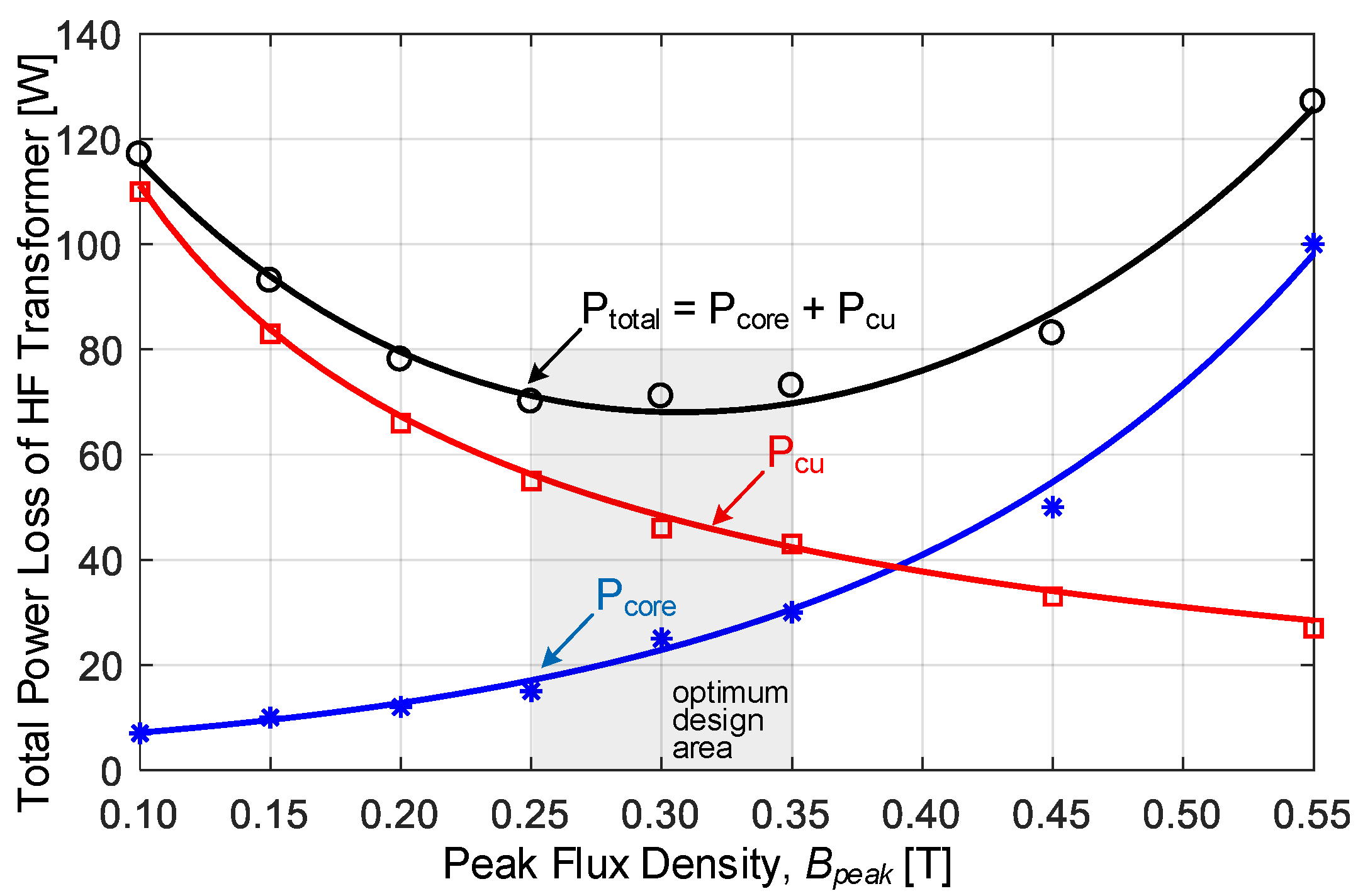
3.3.4. HF Transformer Design

In this application, advanced types of ferrite, amorphous metal cobalt-base, amorphous metal iron-base, and nanocrystalline core materials can be used. Their recommended peak flux densities for operating frequency around 20 kHz are 0.3, 0.5, 1.3, and 1.0 T, respectively. The nanocrystalline core material has lower core loss than ferrite and much lower core loss than high flux density, amorphous metal iron-base material operating at the same peak flux density and frequency. On the other hand, although core loss density of the amorphous metal cobalt-base material is comparable to that of nanocrystalline material, it requires higher core volume resulting in higher total core loss and higher cost because of lower operating flux density. Nanocrystalline core material is therefore chosen in the design of the HF transformer with natural air cooling.
Rated values of the target transformer are specified as 23 kW, 20 kHz rated frequency, 700 V peak secondary voltage, and n = Ns/Np = 1.52. SU102b nanocrystalline core is then used in the implementation of the HF transformer. Core loss, AC copper loss and total power loss of HF transformer against peak flux density are as given in Figure 17. Total power loss variation curve in Figure 17 shows that optimum design point can be chosen in between 0.25 T and 0.35 T. Design of the HF transformer is completed by choosing peak flux density as 0.3 T for minimum power dissipation at 20 kHz.
To test whether the design of MPPT converter is optimum, all power loss components excluding wiring and cabling losses are calculated and given in Figure 18 for three different operating frequencies and maximum PV power in the entire operating range of the MPPT converter installed at the predefined geographical site. Since fsw = 20 kHz causes minimum power loss in the MPPT converter, the optimum design principles given in this subsection are justified.

3.3.5. Controller Design

The block diagram of the implemented DSP (TMS 320F28069) based controller is shown in Figure 3a. The controller is designed to fulfill the following tasks: (i) precharging the DC link capacitors, Co, of the HF link MPPT converter; (ii) MPPT operation; and (iii) overvoltage protection and drain-to-source voltage monitoring for shoot-through protection. For this purpose, DC link voltage, Vdc, and PV panel voltage and current, Vpv and Ipv, are input to the controller, at a sampling rate of 40 kHz/channel. Voltage transducers used are of Fully-Differential Isolation Amplifier (TI AMC-1100) type for noise immunity, and the current transducer is Hall-Effect type (LEM HASS 50-S).
When the sun rises, the PI controller in Figure 3a starts to operate by applying narrow pulses to limit the charging current of Co to a safe value. Precharging period is less than 30 s, during which D does not exceed 0.15. Set value of the DC link voltage, Vdc(set), is specified to be 700 V in the control software. Whenever Vdc reaches 700 V, the inverter control system is activated to start the transfer of power to the grid. Just after the inverter operation, the controller enables MPPT algorithm based on an adaptive version of Perturb and Observe method [75], which runs only once every 300 ms, and stops whenever the error in active power between any two consecutive iterations is less than 0.1%. The algorithm then starts afresh after 1 s. In each iteration, the magnitude of duty ratio perturbation, Δd, is only ±0.25% of the previous duty ratio, D. Sampled Ipv and Vpv data are averaged over a period of 25 ms (256 samples), not only to filter out the measurement noise but also for the use in overvoltage protection software. The inverter tends to keep Vdc constant, and overvoltage protection facility in the controller of MPPT converter does not allow a rise in Vdc more than 10% in the case of loss of control. Furthermore, vDS monitoring is carried out by an analog chip within the SiC driver [76].

4. Field Test Results

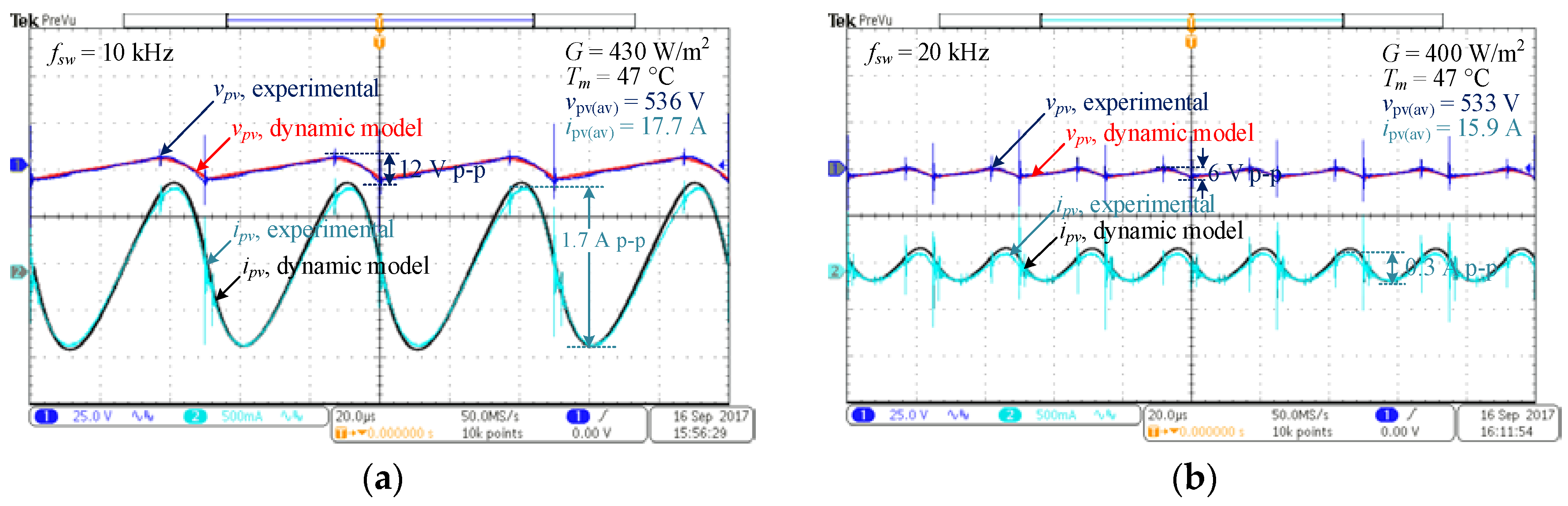
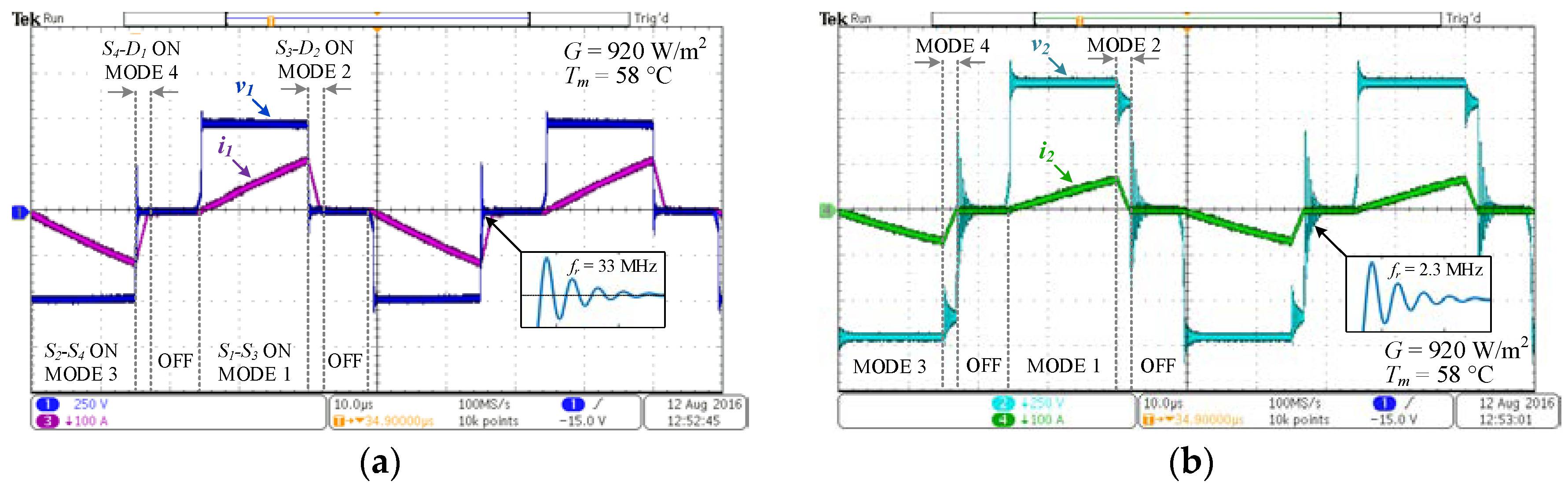
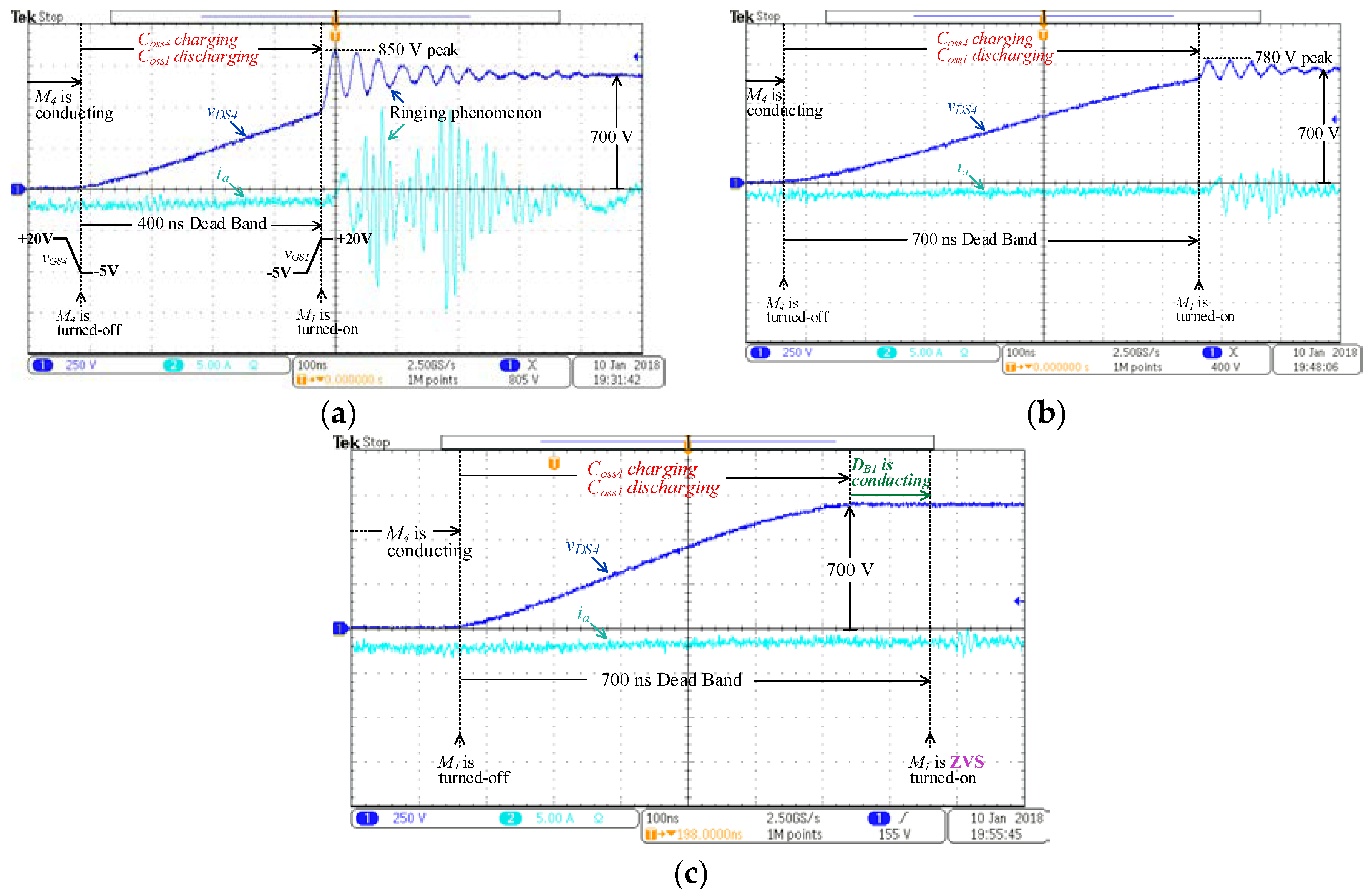
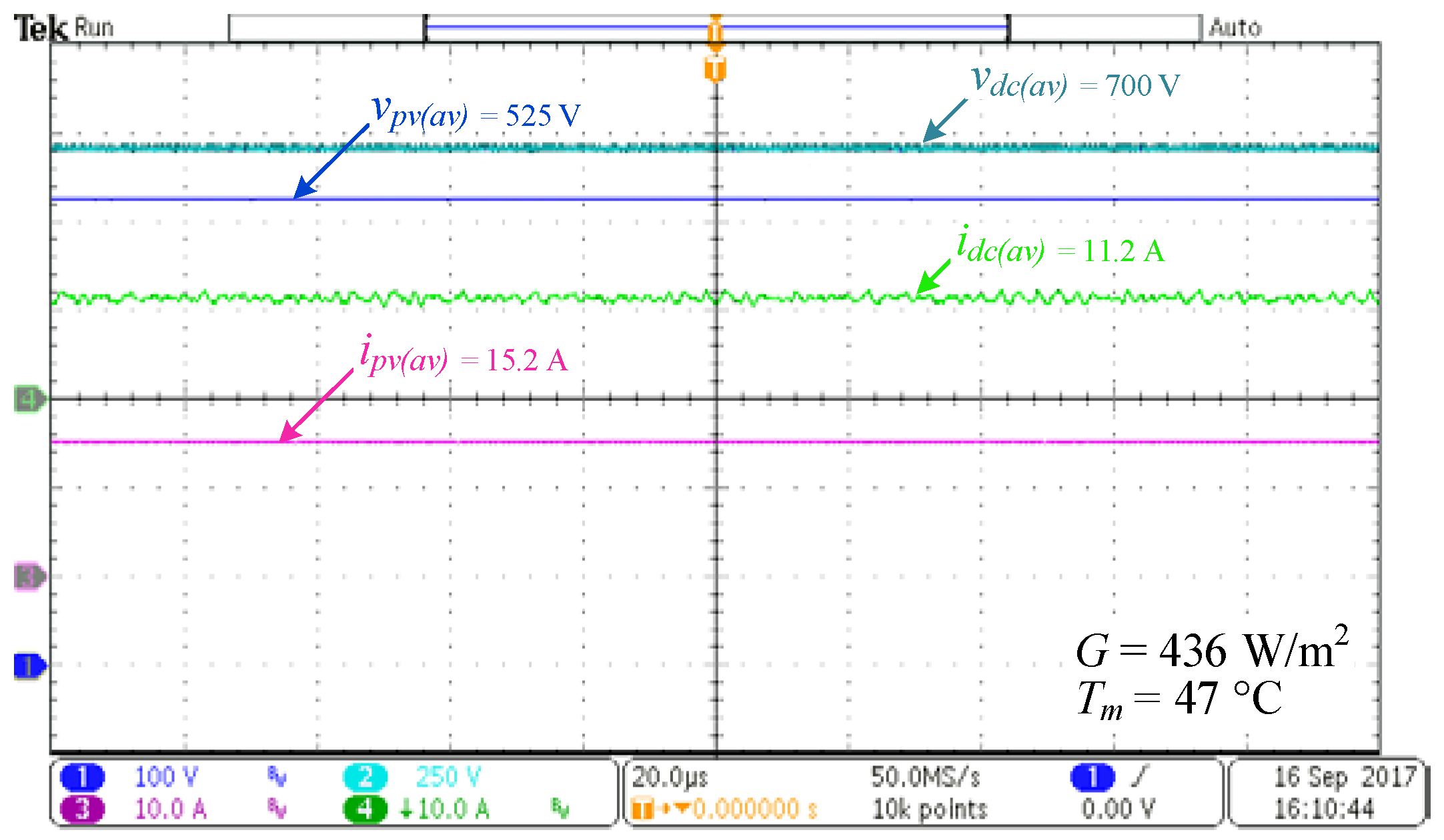
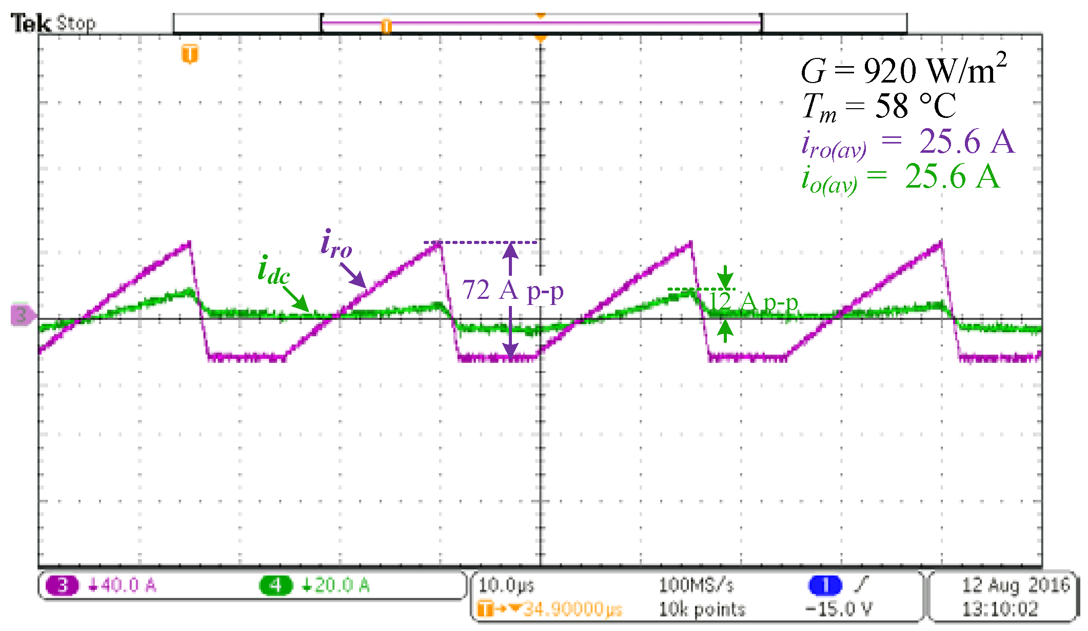
4.1. HF Link MPPT Converter

Variations in ac components of vpv and ipv while the MPPT converter is supplied from the multi-string PV system in Figure 2 are given in Figure 19, for operation at two different switching frequencies. The following observations can be made about these waveforms:
(i)
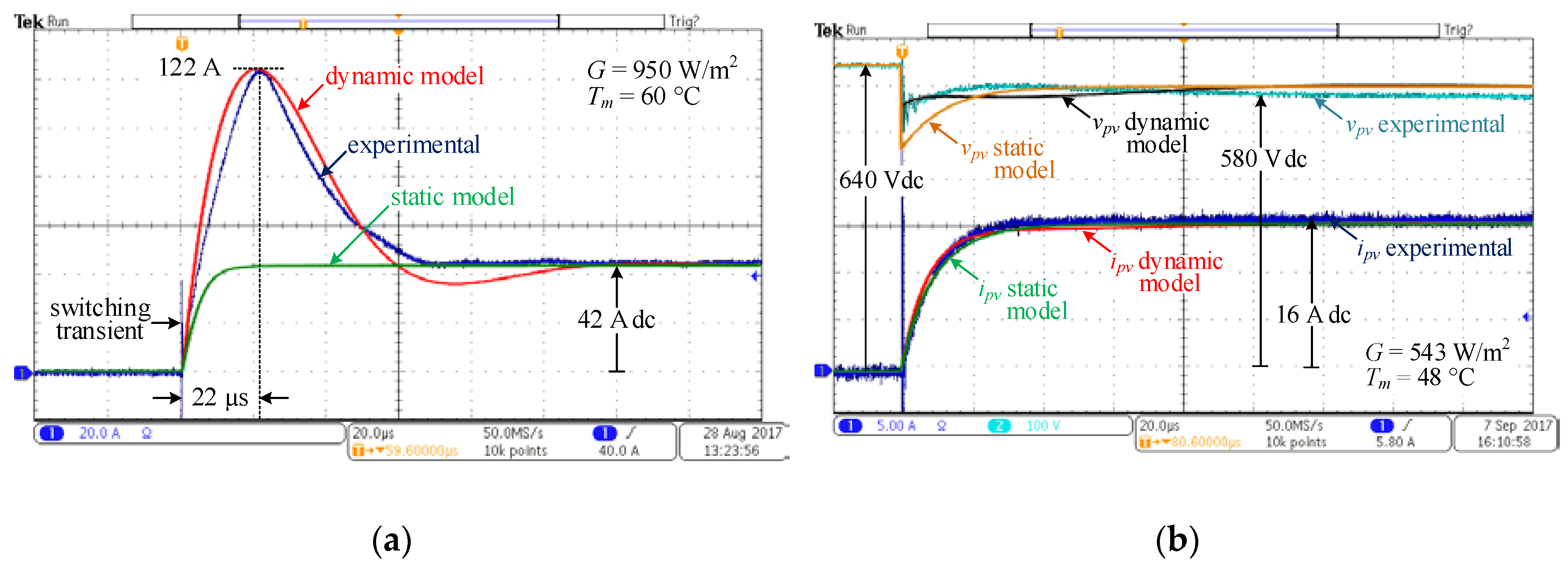
Since the experimental results are the same with the theoretical ones based on the dynamic model of the PV array, the mathematical model and system design methodology can be successfully used in the design of the SiC power MOSFET-based HF link MPPT converter.
(ii)
vpv and ipv are nearly pure DC at fsw = 20 kHz, i.e., only 6 V p-p ripple is superimposed on Vpv(av) = 533 V and 0.3 A p-p ripple is superimposed on Ipv(av) = 15.9 A. This justifies the optimum switching frequency of around 20 kHz, for the SiC HF link converter.
Drain-to-source voltage, vDS, of SiC power MOSFET S3 and the line current i1 waveform of the H-bridge in Figure 3 are also recorded as shown in Figure 20. Positive half cycles of i1 correspond to the drain current id waveform of S3. Note that all SiC power MOSFETs turn-on at zero-current owing to the ramp current waveform of the discontinuous conduction mode. At the turn-off, however, only S3 and S4 are switched at zero current at the end of the OFF period as illustrated in Figure 11b,d, due to the phase shifted operation. S1 and S2, however, are switched off at the peak of the transformer primary current, i1. The glitches superimposed on vDS waveform of S3 in Figure 20 are attributed to the noise coupled to the oscilloscope voltage probe during switching-off of the other SiC power MOSFETs.
HF transformer voltage and current waveforms on both the primary and the secondary sides are as shown in Figure 21, at nearly full-load. Operation modes of the HF link converter, as defined in Figure 11 are marked on various segments of the recorded voltage and current waveforms in Figure 21. The voltage spikes at the turn-off of S1 and S2 (just at the beginning of freewheeling modes of S3-D2 and S4-D1) in Figure 21a are caused by the ringing between switches’ output capacitances (Coss = 880 pF) and the primary stray inductance of the current path between Ci and S1 or S2 (calculated from layout as Lstray1 ≈ 27 nH). The corresponding oscillation frequency is measured as 33 MHz, as expected. This effect is more pronounced at the secondary side waveforms in Figure 21b, owing to the resonance between the two outgoing Schottky diode output capacitances (Cj ≈ 1000 pF each) and the secondary leakage inductance (Ls = 7.4 μH), in series with the stray inductances (Lstray2 ≈ 2.4 μH) between Co and the outgoing diodes, resulting in an oscillation frequency of 2.3 MHz. The slight voltage drops during freewheeling modes in Figure 21b are caused by Lstray2.
AC components of rectifier output current, iro, and the converter output current waveform, idc, in Figure 22 are recorded by a Rogowski current probe. Note that 72 A p-p rectifier output current ripple at full-load is filtered down to 12 A p-p by the low ESR DC link capacitor Co.

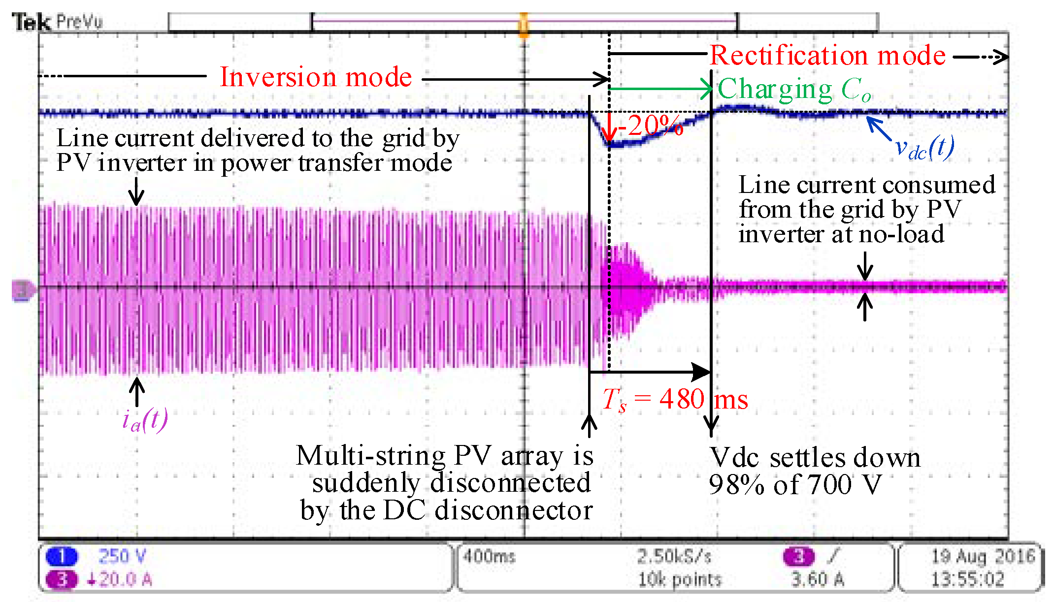
4.2. Voltage Source Inverter

Since the three-phase two-level VSI is built by using a full SiC six-pack module, only the drain-to-source voltages vDS and unfiltered line currents ia, ib, and ic can be recorded. Figure 23 shows the circuit diagram of first leg of the inverter and the associated unfiltered line current, ia. To investigate effects of dead band on the turn-off performance of SiC power MOSFETs, vDS4 and ia are recorded around the zero-crossing point of the unfiltered line-a current waveform for various dead times, as shown in Figure 24. These waveforms are as shown in Figure 24a when dead band is adjusted to 400 ns. Since current is very low, Coss4 and Coss1 are, respectively, charging and discharging slowly. When M1 is turned on at the end of the dead band period, Coss4 is not charged yet to Vdc = 700 V and the Coss1 is not discharged entirely. The residual voltage on Coss1 will then be superimposed on DC link voltage which appears across the drain-source terminals of S4 (vDS4). A shorter dead band causes a larger overshoot on vDS4 waveform. This phenomenon does not occur around the peak value of unfiltered line-a current. This is because Coss4 and Coss1, respectively, charges and discharges more rapidly since the current is high.
On the other hand, ringing phenomenon is observed on vDS4 when S1 is turned on due to the damped high frequency oscillation between the stray inductance of DC bus and Coss1. In general, shorter dead time reduces low order harmonic distortion in line current waveforms at the expense of higher switching loss at turn-on and high frequency harmonic component. As can be seen in Figure 24b, a longer dead time (700 ns) reduces peak value of vDS4 and alleviates ringing phenomenon. At a current level slightly higher than that of Figure 24a,b, 700 ns dead time eliminates entirely ringing phenomenon and leads to ZVS turn-on of M1 as shown in Figure 24c at the expense of higher low order harmonic distortion. In view of these considerations, 400 ns dead time is used in the implementation.
To investigate the transient performance of the VSI control system, multi-string PV system is suddenly disconnected from the input of the MPPT converter while the PV supply is delivering nearly 11 kW to the grid. The recorded filtered line current and the DC link voltage waveforms are as shown in Figure 25. Just after disconnection Vdc makes nearly 20% undershoot and then settles down to 98% of its rated value in nearly 480 ms. It is worth noting that, after reaching minimum Vdc, the voltage source converter starts to operate in rectification mode to allow power transfer from the grid to the DC link, thus maintaining Vdc at 700 V. Transient response is affected primarily by the size of the DC link capacitor and secondarily the LCL filter. Vdc in Figure 25 would decay more rapidly in the case of a smaller Co, thus increasing undershoot in Vdc. To compensate for this phenomenon a larger size LCL filter could be used. A larger LCL filter would allow to increase the control range and hence the voltage source converter could settle down to the new operation state much more rapidly.

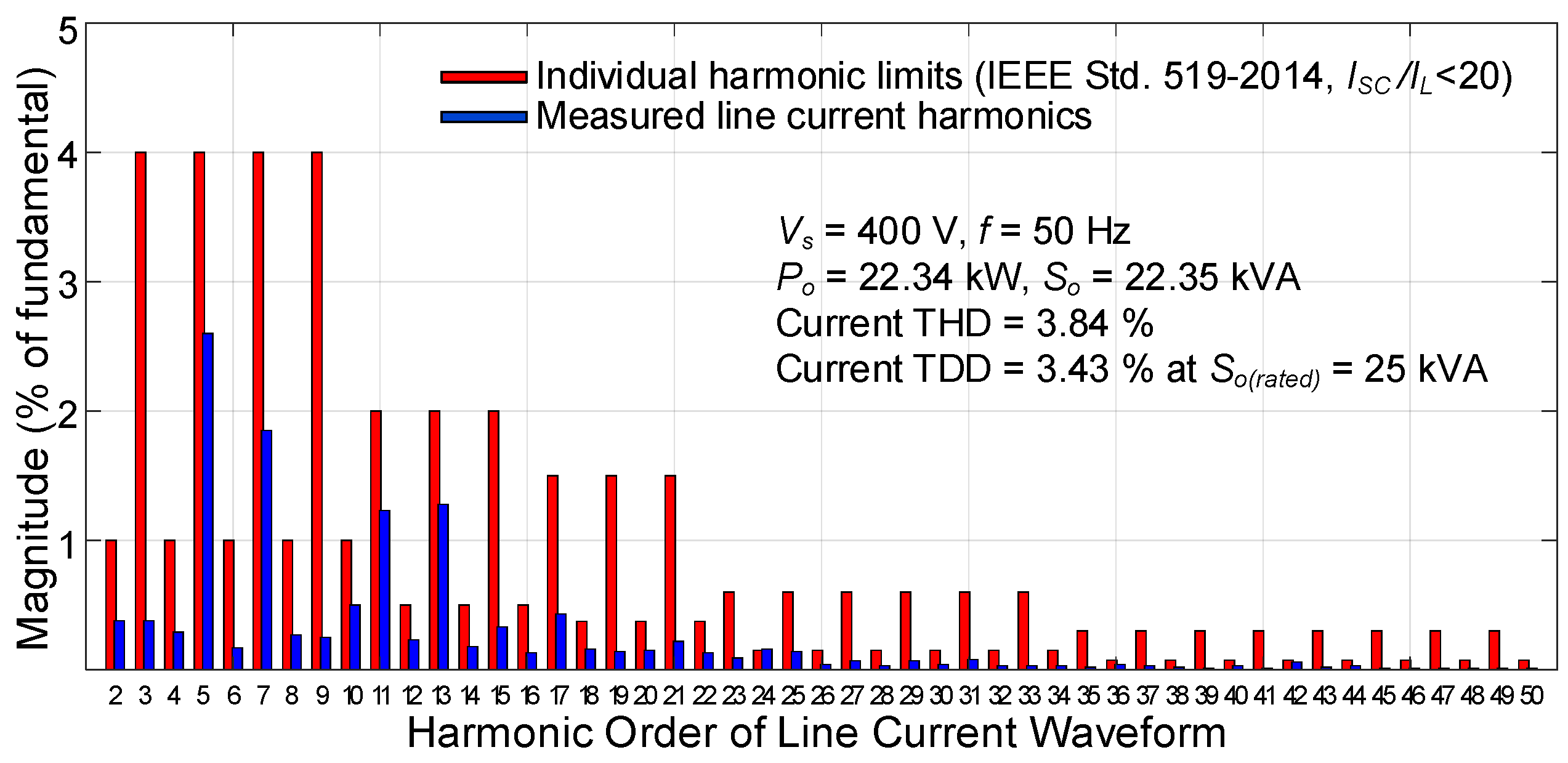
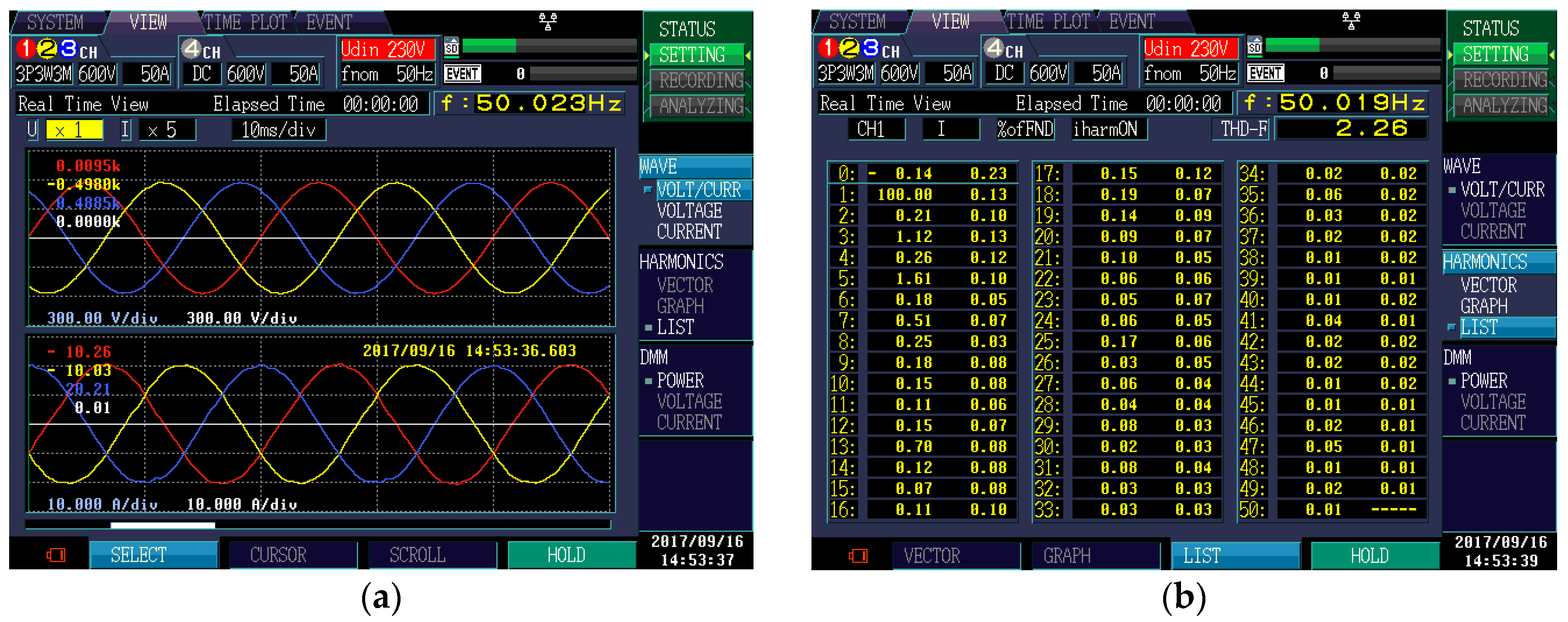
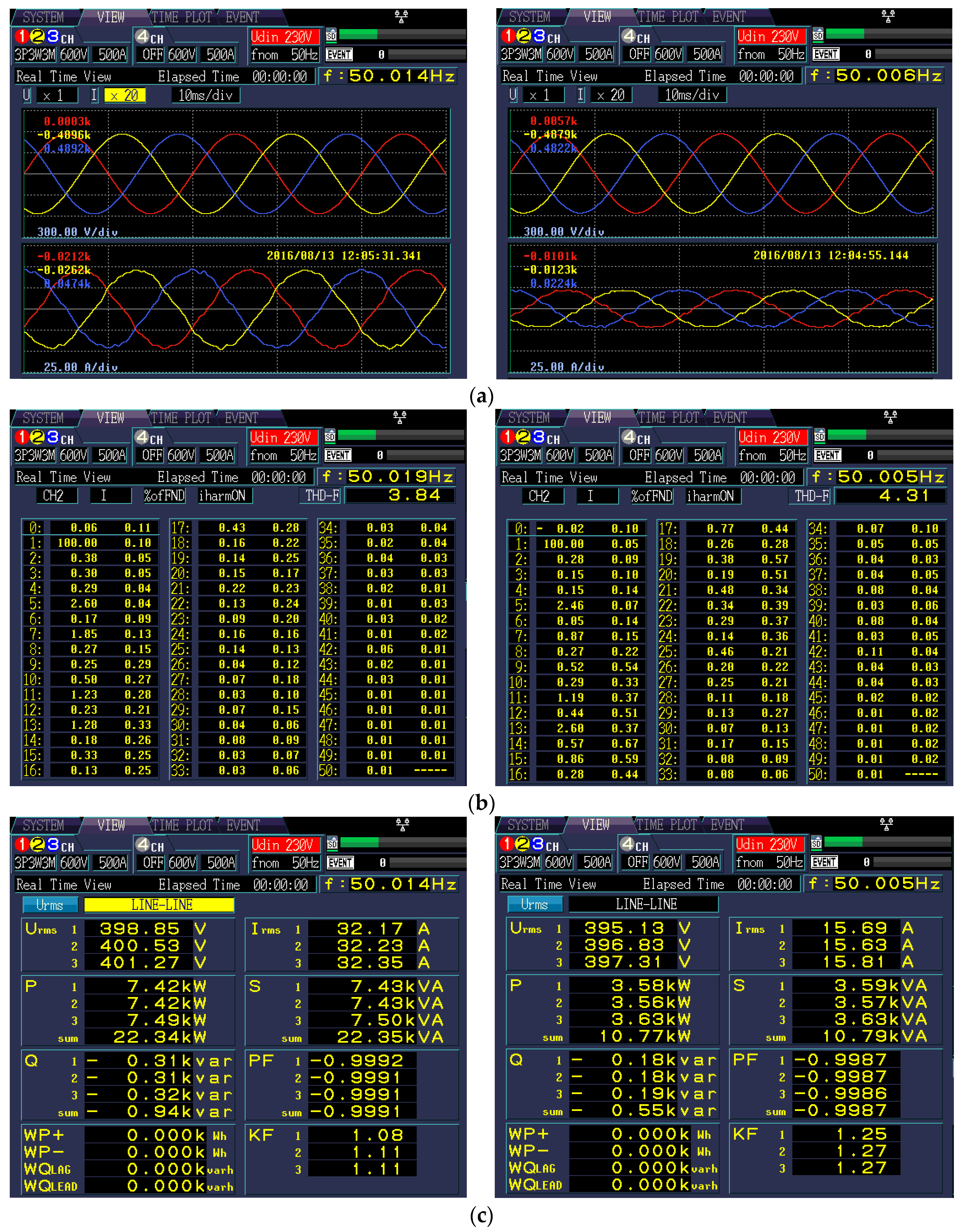
4.3. Harmonic Distortion

Snapshots of the grid-side electrical quantities are given in Figure 26 for operation at full-load (Figure 26, left) and half-load (Figure 26, side). Figure 26a gives the three-phase voltages and line current waveforms, and Figure 26b the associated harmonic current contents according IEC61000-4-7:2002 harmonic measurement method [77], including both the line harmonics and the interharmonics. The rms quantities and output powers are recorded as shown in Figure 26c. The following observations can be made about these waveforms:
  • The inverter operates connected to the 50-Hz AC grid with a total harmonic distortion, THDv ≈ 1.4% for the line-to-line voltages, and dominant 5th and 7th harmonics. The current THDi is recorded to be 3.8% at full-load, and 4.3% at half-load, with dominant 5th and 7th harmonics as in the AC grid. These current THD values correspond to current TDD values, respectively, of 3.4% and 1.9% by taking 25 kVA as the apparent power rating of the VSI.
  • The resulting individual line current harmonics obtained experimentally are found to be within the recommended limits by the IEEE Std.-519-2014 [78] for all supply conditions, as can be seen from Figure 26b and Figure 27 for a harmonic spectrum up to the 50th.
  • The inverter operates successfully at unity pf, (pf ≈ 0.999 recorded), under both the full-load and the half-load conditions, according to the preset value, Iq(set) = 0.
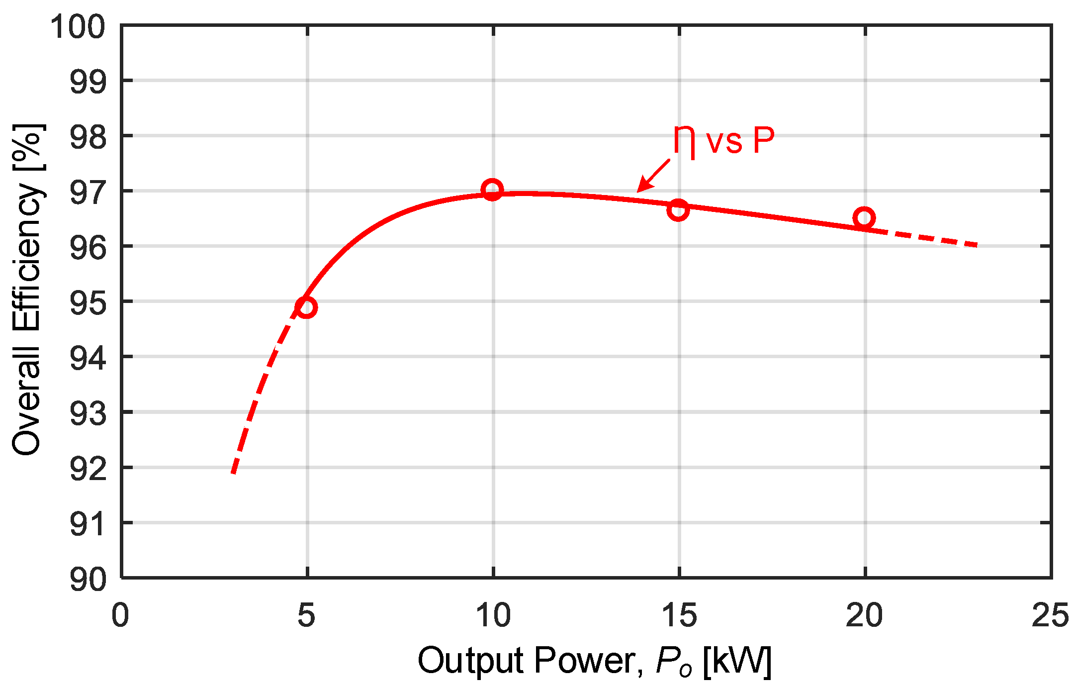
In this research work, the LCL filter is optimized to yield minimum filter size and hence cost. To illustrate the effects of LCL filter size on the harmonic distortion of line current waveforms, Lg is increased from 50 μH to 1.5 mH, as preferred by several researchers in their implementations, and then the harmonic distortion record is repeated at 10 kVA. These records are given in Figure 28. THD and TDD values of the line current waveforms are 2.26% and 0.9%, respectively. It is seen that a larger size and hence more dissipative and costly LCL filter yields much lower harmonic distortion in line current waveforms.

4.4. Efficiency

Efficiencies of HF link MPPT converter, VSI, and the overall grid-connected PV supply are obtained separately by field measurements for different operating conditions. Experimental results are given in comparison with theoretical values. For efficiency calculations, power components Pi, Po(MPPT), and Po are as defined in Figure 29. For different operating conditions, Pi = vpv(av).ipv(av) and Po(MPPT) = vdc(av).idc(av) are calculated from measured vpv(av), ipv(av), vdc(av), and idc(av) data as described in the caption of Figure 29. A sample set of vpv(av), ipv(av), vdc(av), and idc(av) waveforms is given in Figure 30. Experimental efficiency values for the MPPT converter calculated from field data for different operating conditions are given in Table 4. For the corresponding insolation levels and module temperatures, the theoretical efficiency values are also calculated by using the MPPT converter model including the dynamic model of the multi-string PV system and running it on MATLAB Simulink at fsw = 20 kHz. These theoretical values are also marked in Table 4. The following conclusions can be drawn from these results:
(i)
Maximum efficiency occurs at nearly half-load.
(ii)
Full-load efficiency (97.3%) is only 0.5% lower than the maximum efficiency (97.7%).
(iii)
Experimental values are slightly lower than corresponding theoretical values (discrepancies, δƞ ≤ 4% at low power levels and δƞ < 1% at high powers).
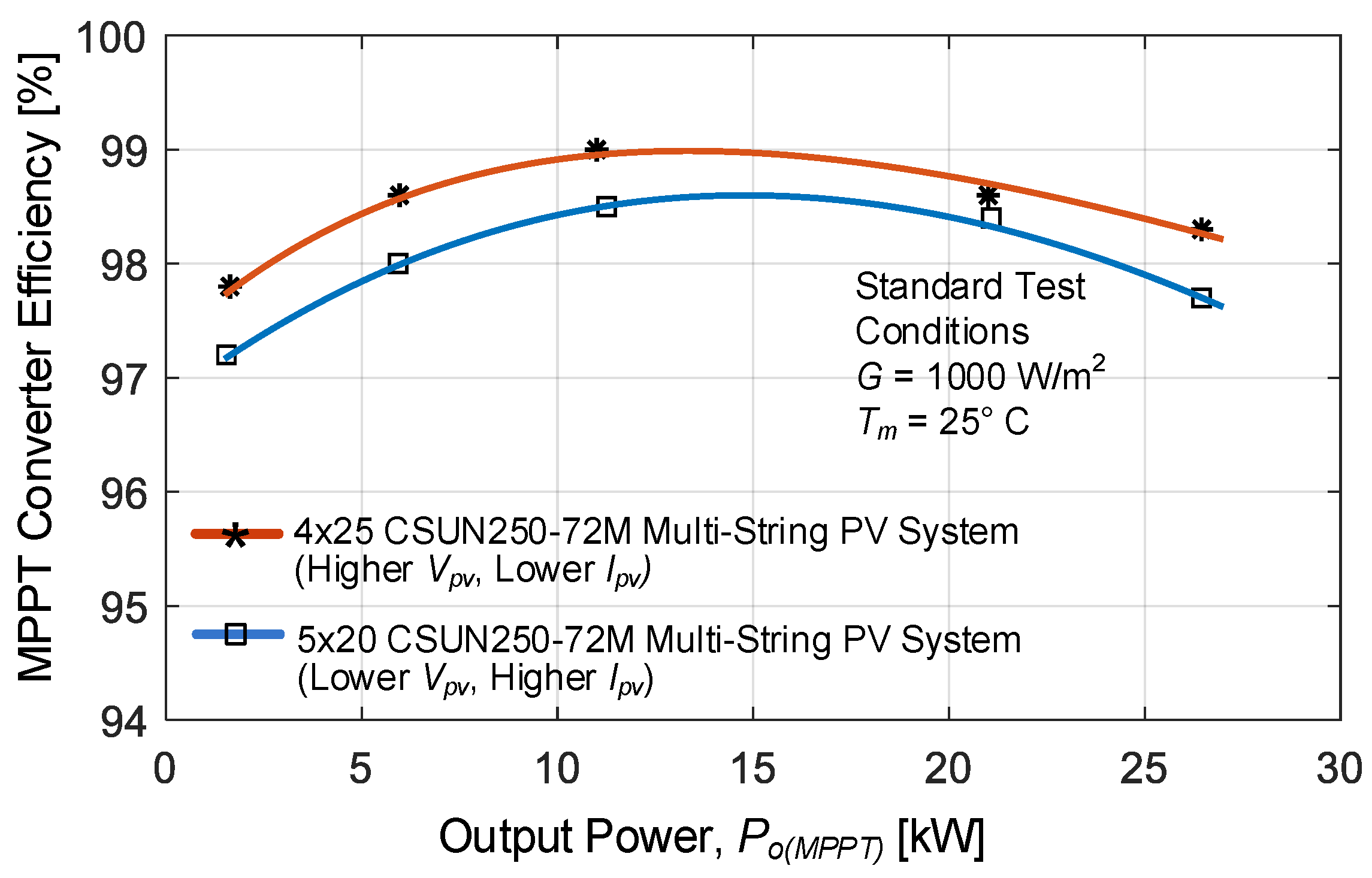
Experimental efficiency values for the SiC VSI calculated from field data for different Po(MPPT) values are given in Table 5. Theoretical values of Po are calculated by subtracting all inverter losses from experimental values of Po(MPPT). For the SiC VSI, computer simulations are carried out using the Wolfspeed SpeedFit design simulation software [72] to calculate SiC MOSFET losses, and Magnetics Inductor Design Tool [79] to determine the LCL filter losses. The following conclusions can be drawn from the results in Table 5:
(i)
Maximum efficiency (98.6%) occurs nearly at 40% of full 22.3 kW-load.
(ii)
Efficiency is 98.1% at 88% of full kW-load.
(iii)
Experimental values are slightly lower than corresponding theoretical values (discrepancies, δƞ ≤ 2% at low power levels and δƞ < 1% at high powers).
The variations in efficiency of the all-SiC PV supply are calculated from field data and given in Figure 31 as a function of Po. Maximum efficiency is observed to be 97%. Full-load efficiency is estimated to be slightly higher than 96%. At very low power levels such as 10% of the full-load, the overall efficiency is around 92%. These efficiency values are comparable with those of new generation PV supplies containing boost type MPPT converters and hybrid IGBT based inverters of the same power ratings and supplied from the existing multi-string PV system in Figure 2.
In the case where the multi-string PV system is initially not available and the types of the modules are not prespecified, the optimum multi-string PV system configuration and its technical characteristics will be a design issue for the overall grid-connected PV supply. The structure and technical characteristics of the multi-string PV system mainly affect the efficiency of the MPPT converter and hence efficiency of the overall system. To illustrate this fact, simulation studies for two different cases which employ 100 CSUN250-72M modules were carried out. In Case 1, 100 modules are connected to give 4 × 25 multi-string PV system to illustrate the effects of high operating voltage and low current on the efficiency of MPPT converter. In Case 2, the same modules are connected to give 5 × 20 multi-string PV system with lower operating voltage and higher current. The simulation results are as given in Figure 32. As can be understood from Figure 32, under standard test conditions, Case 1 gives 99% converter efficiency at nearly half-load and, when it is combined with inverter efficiency, the maximum efficiency of the overall system may reach 98.1%. This is because the operation of the MPPT converter with HF link in Figure 3 at a lower PV current, ipv, reduces conduction loss components remarkably, thus improving the converter efficiency.

5. Conclusions

A system design methodology for an all SiC grid-connected PV supply with HF link MPPT converter has been proposed and a prototype of 25 kVA converter operating at 20 kHz has been implemented for verification. Owing to the very high dv/dt (>10 kV/μs) ratings of SiC power semiconductors, common-mode EMI is more pronounced in SiC based non-isolated converters. In this work, galvanic isolation of the proposed MPPT converter overcomes the common-mode EMI problem, thus enabling the grid connection using a simple and reliable three-phase, two-level inverter. In the design of the HF link MPPT converter operating at 20 kHz, a dynamic model of the multi-string PV system, parameters of which are obtained from the field test results, is used. More realistic MPPT converter parameters are shown to be obtained in the paper by using the dynamic PV model in the design procedure in comparison with the well-known static PV models.
The optimum switching frequency of the 25 kVA three-phase two-level inverter is determined as 20 kHz in the design procedure in view of inverter losses. The resulting 25 kVA, 20 kHz SiC VSI has 98.5% maximum efficiency which is slightly higher than or comparable with those of new-generation IGBT (Si IGBT + antiparallel SiC Schottky Diode) based counterparts for the existing multi-string PV system in Figure 2. This relatively high switching frequency not only reduces the size of the passive components, such as the LCL filter and the HF transformer but also the size of the cooling aggregates. LCL filter of the VSI, which is optimized by considering stability concerns of the controller in the design, provides nearly 100 dB attenuation at 20 kHz and its size is at least ten times smaller than those of LCL filter designs reported in the literature, even for lower size converters. TDD of the grid-connected VSI is measured to be 3.9% at nearly full-load and its individual current harmonics up to 50th conform with IEC Std. 61000-4-7:2002 even for the weakest grid. A higher grid-side inductance (Lg = 1.5 mH) of the LCL filter lowers the current THDs considerably, which is measured to be 2.3% at nearly half-load.
The resulting SiC MPPT converter operating at 20 kHz and supplied from the existing 5 × 19 multi-string PV system in Figure 2 has 98% measured maximum efficiency, which is comparable with IGBT based and lower than SiC based boost type MPPT converters. Power densities are calculated as nearly 1.8 kW/lt and 1.6 kW/lt for forced air-cooled SiC MPPT converter and SiC grid-connected VSI, respectively. These figures are higher than those of forced air-cooled new-generation IGBT based converters and much higher than those of natural air-cooled new-generation IGBT based converters.

Author Contributions

M.E. and I.Ç. conceived the presented idea. M.C. and M.E. developed and implemented the SiC inverter. S.Ö. and I.Ç. developed and implemented the SiC MPPT converter. All authors discussed the results and contributed to the final manuscript.

Funding

This research was funded by Scientific Research Projects Office of Middle East Technical University for the development of SiC inverter with grant number BAP-03-01-2014-005, and ARTI Industrial Electronics Ltd. for the development of MPPT converter with HF link and multi-string PV system with grant number M.EE.P86.

Acknowledgments

The authors would like to acknowledge Energy Institute, TUBITAK Marmara Research Center, Ankara branch for the scholarship provided to M.C. for the research on SiC converters.

Conflicts of Interest

The authors declare no conflicts of interest.

References

  1. Kjaer, S.B.; Pedersen, J.K.; Blaabjerg, F. A review of single-phase grid-connected inverters for photovoltaic modules. IEEE Trans. Ind. Appl. 2005, 41, 1292–1306. [Google Scholar] [CrossRef]
  2. Mechouma, R.; Azoui, B.; Chaabane, M. Three-phase grid connected inverter for photovoltaic systems, a review. In Proceedings of the 2012 First International Conference on Renewable Energies and Vehicular Technology, Hammamet, Tunisia, 26–28 March 2012; pp. 37–42. [Google Scholar]
  3. Orłowska-Kowalska, T.; Frede, B.; José, R. Advanced and Intelligent Control in Power Electronics and Drives; Springer: Berlin, Germany, 2014. [Google Scholar]
  4. Barater, D.; Lorenzani, E.; Concari, C.; Franceschini, G.; Buticchi, G. Recent advances in single-phase transformerless photovoltaic inverters. IET Renew. Power Gener. 2016, 10, 260–273. [Google Scholar] [CrossRef]
  5. Chen, S.M.; Liang, T.J.; Yang, L.S.; Chen, J.F. A Boost Converter with Capacitor Multiplier and Coupled Inductor for AC Module Applications. IEEE Trans. Ind. Electron. 2013, 60, 1503–1511. [Google Scholar] [CrossRef]
  6. Liao, C.Y.; Lin, W.S.; Chen, Y.M.; Chou, C.Y. A PV Micro-inverter With PV Current Decoupling Strategy. IEEE Trans. Power Electron. 2017, 32, 6544–6557. [Google Scholar] [CrossRef]
  7. Villanueva, E.; Correa, P.; Rodriguez, J.; Pacas, M. Control of a Single-Phase Cascaded H-Bridge Multilevel Inverter for Grid-Connected Photovoltaic Systems. IEEE Trans. Ind. Electron. 2009, 56, 4399–4406. [Google Scholar] [CrossRef]
  8. Lorenzani, E.; Immovilli, F.; Migliazza, G.; Frigieri, M.; Bianchini, C.; Davoli, M. CSI7: A Modified Three-Phase Current-Source Inverter for Modular Photovoltaic Applications. IEEE Trans. Ind. Electron. 2017, 64, 5449–5459. [Google Scholar] [CrossRef]
  9. Chen, Y.M.; Lo, K.Y.; Chang, Y.R. Multi-string single-stage grid-connected inverter for PV system. In Proceedings of the 2011 IEEE Energy Conversion Congress and Exposition, Phoenix, AZ, USA, 17–22 September 2011; pp. 2751–2756. [Google Scholar]
  10. Edrington, C.S.; Balathandayuthapani, S.; Cao, J. Analysis and control of a multi-string photovoltaic (PV) system interfaced with a utility grid. In Proceedings of the IEEE PES General Meeting, Minneapolis, MN, USA, 25–29 July 2010; pp. 1–6. [Google Scholar]
  11. SMA, SUNNY CENTRAL—High Tech Solution for Solar Power Stations. Products Category Brochure. Available online: http://www.sma-america.com/ (accessed on 21 February 2018).
  12. Subudhi, B.; Pradhan, R. A Comparative Study on Maximum Power Point Tracking Techniques for Photovoltaic Power Systems. IEEE Trans. Sustain. Energy 2013, 4, 89–98. [Google Scholar] [CrossRef]
  13. Müller, N.; Renaudineau, H.; Flores-Bahamonde, F.; Kouro, S.; Wheeler, P. Ultracapacitor storage enabled global MPPT for photovoltaic central inverters. In Proceedings of the 2017 IEEE 26th International Symposium on Industrial Electronics (ISIE), Edinburgh, UK, 19–21 June 2017; pp. 1046–1051. [Google Scholar]
  14. Miguel, C.; Fernando, M.; Riganti, F.F.; Antonino, L.; Alessandro, S. A neural networks-based maximum power point tracker with improved dynamics for variable dc-link grid-connected photovoltaic power plants. Int. J. Appl. Electromagn. Mech. 2013, 43, 127–135. [Google Scholar]
  15. Mancilla-David, F.; Arancibia, A.; Riganti-Fulginei, F.; Muljadi, E.; Cerroni, M. A maximum power point tracker variable-dc-link three-phase inverter for grid-connected PV panels. In Proceedings of the 2012 3rd IEEE PES Innovative Smart Grid Technologies Europe (ISGT Europe), Berlin, Germany, 14–17 October 2012; pp. 1–7. [Google Scholar]
  16. Kerekes, T.; Teodorescu, R.; Liserre, M.; Klumpner, C.; Sumner, M. Evaluation of Three-Phase Transformerless Photovoltaic Inverter Topologies. IEEE Trans. Power Electron. 2009, 24, 2202–2211. [Google Scholar] [CrossRef]
  17. Walker, G.R.; Sernia, P.C. Cascaded DC-DC converter connection of photovoltaic modules. IEEE Trans. Power Electron. 2004, 19, 1130–1139. [Google Scholar] [CrossRef]
  18. Koutroulis, E.; Blaabjerg, F. Design Optimization of Transformerless Grid-Connected PV Inverters Including Reliability. IEEE Trans. Power Electron. 2013, 28, 325–335. [Google Scholar] [CrossRef]
  19. Meneses, D.; Blaabjerg, F.; García, Ó.; Cobos, J.A. Review and Comparison of Step-Up Transformerless Topologies for Photovoltaic AC-Module Application. IEEE Trans. Power Electron. 2013, 28, 2649–2663. [Google Scholar] [CrossRef]
  20. Araujo, S.V.; Zacharias, P.; Mallwitz, R. Highly Efficient Single-Phase Transformerless Inverters for Grid-Connected Photovoltaic Systems. IEEE Trans. Ind. Electron. 2010, 57, 3118–3128. [Google Scholar] [CrossRef]
  21. Zhang, L.; Sun, K.; Xing, Y.; Xing, M. H6 Transformerless Full-Bridge PV Grid-Tied Inverters. IEEE Trans. Power Electron. 2014, 29, 1229–1238. [Google Scholar] [CrossRef]
  22. Rodriguez, J.; Bernet, S.; Steimer, P.K.; Lizama, I.E. A Survey on Neutral-Point-Clamped Inverters. IEEE Trans. Ind. Electron. 2010, 57, 2219–2230. [Google Scholar] [CrossRef]
  23. Bala, S. Next Gen PV Inverter Systems Using WBG Devices. In High Pen PV Through Next-Gen PE Technologies Workshop; NREL: Golden, CO, USA, 2016. [Google Scholar]
  24. Millán, J.; Godignon, P.; Perpiñà, X.; Pérez-Tomás, A.; Rebollo, J. A Survey of Wide Bandgap Power Semiconductor Devices. IEEE Trans. Power Electron. 2014, 29, 2155–2163. [Google Scholar] [CrossRef]
  25. Mookken, J.; Agrawal, B.; Liu, J. Efficient and Compact 50 kW Gen2 SiC Device Based PV String Inverter. In Proceedings of the International Exhibition and Conference for Power Electronics, Intelligent Motion, Renewable Energy and Energy Management, Nuremberg, Germany, 20–22 May 2014; pp. 1–7. [Google Scholar]
  26. Wei, S.; He, F.; Yuan, L.; Zhao, Z.; Lu, T.; Ma, J. Design and implementation of high efficient two-stage three-phase/level isolated PV converter. In Proceedings of the 18th International Conference on Electrical Machines and Systems (ICEMS), Pattaya, Thailand, 25–28 October 2015; pp. 1649–1654. [Google Scholar]
  27. Shi, Y.; Li, R.; Xue, Y.; Li, H. High-Frequency-Link-Based Grid-Tied PV System With Small DC-Link Capacitor and Low-Frequency Ripple-Free Maximum Power Point Tracking. IEEE Trans. Power Electron. 2016, 31, 328–339. [Google Scholar] [CrossRef]
  28. Islam, M.; Mekhilef, S. Efficient Transformerless MOSFET Inverter for a Grid-Tied Photovoltaic System. IEEE Trans. Power Electron. 2016, 31, 6305–6316. [Google Scholar] [CrossRef]
  29. Sintamarean, N.C.; Blaabjerg, F.; Wang, H.; Yang, Y. Real Field Mission Profile Oriented Design of a SiC-Based PV-Inverter Application. IEEE Trans. Ind. Appl. 2014, 50, 4082–4089. [Google Scholar] [CrossRef]
  30. Shi, Y.; Wang, L.; Xie, R.; Shi, Y.; Li, H. A 60-kW 3-kW/kg Five-Level T-Type SiC PV Inverter With 99.2% Peak Efficiency. IEEE Trans. Ind. Electron. 2017, 64, 9144–9154. [Google Scholar] [CrossRef]
  31. Colmenares, J.; Peftitsis, D.; Rabkowski, J.; Sadik, D.P.; Tolstoy, G.; Nee, H.P. High-Efficiency 312-kVA Three-Phase Inverter Using Parallel Connection of Silicon Carbide MOSFET Power Modules. IEEE Trans. Ind. Appl. 2015, 51, 4664–4676. [Google Scholar] [CrossRef]
  32. Rabkowski, J.; Peftitsis, D.; Nee, H.P. Design steps towards a 40-kVA SiC inverter with an efficiency exceeding 99.5%. In Proceedings of the Twenty-Seventh Annual IEEE Applied Power Electronics Conference and Exposition (APEC), Orlando, FL, USA, 5–9 February 2012; pp. 1536–1543. [Google Scholar]
  33. Yin, S.; Tseng, K.J.; Tong, C.F.; Simanjorang, R.; Gajanayake, C.J.; Gupta, A.K. A 99% efficiency SiC three-phase inverter using synchronous rectification. In Proceedings of the IEEE Applied Power Electronics Conference and Exposition (APEC), Long Beach, CA, USA, 20–24 March 2016; pp. 2942–2949. [Google Scholar]
  34. Laird, Y.Y.I.; Yuan, X.; Scoltock, J.; Forsyth, A.J. A Design Optimization Tool for Maximizing the Power Density of 3-Phase DC–AC Converters Using Silicon Carbide (SiC) Devices. IEEE Trans. Power Electron. 2018, 33, 2913–2932. [Google Scholar] [CrossRef]
  35. Payan, D.; Catani, J.P.; Schwander, D. Solar Array Dynamic Simulator Prevention of Solar Array Short-Circuits due to Electrostatic Discharge. In Proceedings of the Space Power, Sixth European Conference, Porto, Portugal, 6–10 May 2002; pp. 609–615. [Google Scholar]
  36. Schwander, D. Dynamic Solar Cell Measurement Techniques: New Small Signal Measurement Techniques. In Proceedings of the Space Power, Sixth European Conference, Porto, Portugal, 6–10 May 2002; pp. 603–608. [Google Scholar]
  37. Blok, R.; van den Berg, E.; Slootweg, D. Solar Cell Capacitance Measurement. In Proceedings of the Space Power, Sixth European Conference, Porto, Portugal, 6–10 May 2002; pp. 597–602. [Google Scholar]
  38. Herman, M.; Jankovec, M.; Topic, M. Optimisation of the I-V measurement scan time through dynamic modelling of solar cells. IET Renew. Power Gener. 2013, 7, 63–70. [Google Scholar] [CrossRef]
  39. Qin, L.; Xie, S.; Yang, C.; Cao, J. Dynamic model and dynamic characteristics of solar cell. In Proceedings of the IEEE ECCE Asia Downunder, Melbourne, Australia, 3–6 June 2013; pp. 659–663. [Google Scholar]
  40. Bharadwaj, P.; Kulkarni, A.; John, V. Impedance estimation of photovoltaic modules for inverter start-up analysis. Sadhana—Acad. Proc. Eng. Sci. 2017, 42, 1377–1387. [Google Scholar] [CrossRef]
  41. Huang, J.H.; Lehman, B.; Qian, T. Submodule integrated boost DC-DC converters with no external input capacitor or input inductor for low power photovoltaic applications. In Proceedings of the IEEE Energy Conversion Congress and Exposition (ECCE), Milwaukee, WI, USA, 18–22 September 2016; pp. 1–7. [Google Scholar]
  42. Duan, S.; Yan, G.; Jin, L.; Ren, J.; Wu, W. Design of photovoltaic power generation mppt controller based on SIC MOSFET. In Proceedings of the TENCON 2015–IEEE Region 10 Conference, Macao, China, 1–4 November 2015; pp. 1–5. [Google Scholar]
  43. Kim, T.; Jang, M.; Agelidis, V.G. Practical implementation of a silicon carbide-based 300 kHz, 1.2 kW hard-switching boost-converter and comparative thermal performance evaluation. IET Power Electron. 2015, 8, 333–341. [Google Scholar] [CrossRef]
  44. Mouli, G.R.C.; Schijffelen, J.H.; Bauer, P.; Zeman, M. Design and Comparison of a 10-kW Interleaved Boost Converter for PV Application Using Si and SiC Devices. IEEE J. Emerg. Sel. Top. Power Electron. 2017, 5, 610–623. [Google Scholar] [CrossRef]
  45. Anthon, Y.Y.A.; Zhang, Z.; Andersen, M.A.E. A high power boost converter for PV Systems operating up to 300 kHz using SiC devices. In Proceedings of the International Power Electronics and Application Conference and Exposition, Shanghai, China, 5–8 November 2014; pp. 302–307. [Google Scholar]
  46. Mostaghimi, O.; Wright, N.; Horsfall, A. Design and performance evaluation of SiC based DC-DC converters for PV applications. In Proceedings of the IEEE Energy Conversion Congress and Exposition (ECCE), Raleigh, NC, USA, 15–20 September 2012; pp. 3956–3963. [Google Scholar]
  47. Fujii, K.; Noto, Y.; Oshima, M.; Okuma, Y. 1-MW solar power inverter with boost converter using all SiC power module. In Proceedings of the 17th European Conference on Power Electronics and Applications (EPE’15 ECCE-Europe), Geneva, Switzerland, 8–10 September 2015; pp. 1–10. [Google Scholar]
  48. Agamy, M.S.; Chi, S.; Elasser, A.; Harfman-Todorovic, M.; Jiang, Y.; Mueller, F.; Tao, F. A High-Power-Density DC–DC Converter for Distributed PV Architectures. IEEE J. Photovolt. 2013, 3, 791–798. [Google Scholar] [CrossRef]
  49. Akagi, H.; Yamagishi, T.; Tan, N.M.L.; Kinouchi, S.I.; Miyazaki, Y.; Koyama, M. Power-Loss Breakdown of a 750-V 100-kW 20-kHz Bidirectional Isolated DC–DC Converter Using SiC-MOSFET/SBD Dual Modules. IEEE Trans. Ind. Appl. 2015, 51, 420–428. [Google Scholar] [CrossRef]
  50. Liserre, M.; Blaabjerg, F.; Dell’Aquila, A. Step-by-step design procedure for a grid-connected three-phase PWM voltage source converter. Int. J. Electron. 2004, 91, 445–460. [Google Scholar] [CrossRef]
  51. Wu, W.; He, Y.; Tang, T.; Blaabjerg, F. A New Design Method for the Passive Damped LCL and LLCL Filter-Based Single-Phase Grid-Tied Inverter. IEEE Trans. Ind. Electron. 2013, 60, 4339–4350. [Google Scholar] [CrossRef]
  52. Peña-Alzola, R.; Liserre, M.; Blaabjerg, F.; Sebastián, R.; Dannehl, J.; Fuchs, F.W. Analysis of the Passive Damping Losses in LCL-Filter-Based Grid Converters. IEEE Trans. Power Electron. 2013, 28, 2642–2646. [Google Scholar] [CrossRef]
  53. Reznik, Y.Y.A.; Simões, M.G.; Al-Durra, A.; Muyeen, S.M. LCL Filter Design and Performance Analysis for Grid-Interconnected Systems. IEEE Trans. Ind. Appl. 2014, 50, 1225–1232. [Google Scholar] [CrossRef]
  54. Liu, J.; Zhou, L.; Yu, X.; Li, B.; Zheng, C. Design and analysis of an LCL circuit-based three-phase grid-connected inverter. IET Power Electron. 2017, 10, 232–239. [Google Scholar] [CrossRef]
  55. Parker, S.G.; McGrath, B.P.; Holmes, D.G. Regions of Active Damping Control for LCL Filters. IEEE Trans. Ind. Appl. 2014, 50, 424–432. [Google Scholar] [CrossRef]
  56. Jayalath, S.; Hanif, M. Generalized LCL-Filter Design Algorithm for Grid-Connected Voltage-Source Inverter. IEEE Trans. Ind. Electron. 2017, 64, 1905–1915. [Google Scholar] [CrossRef]
  57. Figueres, E.; Garcera, G.; Sandia, J.; Gonzalez-Espin, F.; Rubio, J.C. Sensitivity Study of the Dynamics of Three-Phase Photovoltaic Inverters With an LCL Grid Filter. IEEE Trans. Ind. Electron. 2009, 56, 706–717. [Google Scholar] [CrossRef]
  58. Timbus, Y.Y.A.; Liserre, M.; Teodorescu, R.; Rodriguez, P.; Blaabjerg, F. Evaluation of Current Controllers for Distributed Power Generation Systems. IEEE Trans. Power Electron. 2009, 24, 654–664. [Google Scholar] [CrossRef]
  59. Blaabjerg, F.; Teodorescu, R.; Liserre, M.; Timbus, A.V. Overview of Control and Grid Synchronization for Distributed Power Generation Systems. IEEE Trans. Ind. Electron. 2006, 53, 1398–1409. [Google Scholar] [CrossRef]
  60. Vasquez, J.C.; Guerrero, J.M.; Savaghebi, M.; Eloy-Garcia, J.; Teodorescu, R. Modeling, Analysis, and Design of Stationary-Reference-Frame Droop-Controlled Parallel Three-Phase Voltage Source Inverters. IEEE Trans. Ind. Electron. 2013, 60, 1271–1280. [Google Scholar] [CrossRef]
  61. Bosch, S.; Steinhart, H. Active power filter with model based predictive current control in natural and dq frame. In Proceedings of the 18th European Conference on Power Electronics and Applications (EPE’16 ECCE Europe), Karlsruhe, Germany, 5–9 September 2016; pp. 1–10. [Google Scholar]
  62. Liserre, M.; Teodorescu, R.; Blaabjerg, F. Multiple harmonics control for three-phase grid converter systems with the use of PI-RES current controller in a rotating frame. IEEE Trans. Power Electron. 2006, 21, 836–841. [Google Scholar] [CrossRef]
  63. Silicon carbide Power Module-BSM300D12P2E001. Available online: http://www.rohm.com/web/global/products/-/product/BSM300D12P2E001 (accessed on 21 February 2018).
  64. CAS325M12HM2 1200V, 325A, Silicon Carbide High-Performance-Wolfspeed. Available online: https://www.wolfspeed.com/cas325m12hm2 (accessed on 21 February 2018).
  65. SKM500MB120SC–SEMIKRON. Available online: https://www.semikron.com/products/product-classes/sic/full-sic/detail/skm500mb120sc-21919770.html (accessed on 21 February 2018).
  66. SiC POWER MODULES. Available online: http://www.mitsubishielectric.com/semiconductors/catalog/pdf/sicpowermodule_e_201505.pdf (accessed on 21 February 2018).
  67. IEC Standard for Power Transformers; IEC Standard IEC 60076-1:2011; IEC Webstore; IEC: Geneva, Switzerland, 2011.
  68. IEC Standard for Standard Voltages; IEC Standard IEC 60038 2002-07; IEC Webstore; IEC: Geneva, Switzerland, 2002.
  69. Kimball, J.W.; Zawodniok, M. Reducing Common-Mode Voltage in Three-Phase Sine-Triangle PWM with Interleaved Carriers. IEEE Trans. Power Electron. 2011, 26, 2229–2236. [Google Scholar] [CrossRef]
  70. Feng, J.; Wang, H.; Xu, J.; Su, M.; Gui, W.; Li, X. A Three-Phase Grid-Connected Micro-Inverter for AC Photovoltaic Module Applications. IEEE Trans. Power Electron. 2017. [Google Scholar] [CrossRef]
  71. Shi, Y.; Wang, L.; Li, H. Stability Analysis and Grid Disturbance Rejection for a 60 kW SiC based Filter-less Grid-connected PV Inverter. IEEE Trans. Ind. Appl. 2017. [Google Scholar] [CrossRef]
  72. SpeedFit Design Simulator™, USA: Wolfspeed. Available online: https://www.wolfspeed.com/speedfit (accessed on 24 February 2018).
  73. Cree, Inc. CREE Application Note, Design Considerations for Designing with Cree SiC Modules; Cree: Durham, NC, USA, 2013. [Google Scholar]
  74. Metallized Polypropylene Film Capacitors (MKP). Available online: http://www.mouser.com/ds/ 2/136/MKP_B32774_778-19326.pdf (accessed on 24 February 2018).
  75. Piegari, L.; Rizzo, R. Adaptive perturb and observe algorithm for photovoltaic maximum power point tracking. IET Renew. Power Gener. 2010, 4, 317–328. [Google Scholar] [CrossRef]
  76. 1ED020I12_F2-DS-v02. Available online: https://www.infineon.com/dgdl/Infineon-1ED020I12_F2-DS-v02_00-en.pdf?fileId=db3a304330f68606013122ce5f3649cb (accessed on 24 February 2018).
  77. IEC Standard for Electromagnetic Compatibility (EMC)—Part 4–7: Testing and Measurement Techniques—General Guide on Harmonics and Interharmonics Measurements and Instrumentation, for Power Supply Systems and Equipment Connected Thereto; IEC Standard IEC 61000-4-7:2002; IEC Webstore; IEC: Geneva, Switzerland, 2002.
  78. IEEE Standard for Recommended Practice and Requirements for Harmonic Control in Electric Power Systems; IEEE Std. 519-2014; IEEE Standards Association: Piscataway, NJ, USA, 2014.
  79. Magnetics® Inductor Design Tool, USA: Magnetics. Available online: https://www.mag-inc.com/Design/Design-Tools/Inductor-Design (accessed on 24 February 2018).
Figure 1. All SiC three-phase grid-connected PV supply with high-frequency link: (a) Multi-string PV inverter system; and (b) Experimental set-up.
Electronics 07 00085 g001
Figure 2. Roof-mounted 23.7 kW at 1000 W/m2 and 25 °C multi-string PV system containing 95 CSUN250-72M modules (five parallel connected strings of 19 series modules; with adjustable tilt angles of 15°, 30°, 45° and 60°); coordinates 39.890917, 32.782278; five modules in the photograph are idle; terminal box of the system inside the laboratory is shown at the right bottom corner of photograph while the pyranometer is at left bottom corner.
Electronics 07 00085 g002
Figure 3. All SiC MPPT converter with high-frequency link: (a) power stage and its control circuitry; (b) yop view of the developed hardware; and (c) side view. (1) Metal Film 30//30 μF Input Capacitor Bank (EPCOS B32778G0306K); (2) All-SiC Half Bridge Module (CREE CAS120M12BM2); (3) Nanocrystalline Core (SU-102b) Based HF Transformer; (4) SiC Schottky Diode (CREE C4D40120D); (5) Dual Channel SiC MOSFET Driver (CREE CGD15HB62P); (6) Fully-Differential Isolation Amplifier (TI AMC-1100); (7) Hall-Effect Current Transducer (LEM HASS 50-S); (8) Microcontroller (TI TMS320F28069); (9) Electrolytic 3400 μF Output Capacitors (EPCOS B43456-A9688-M).
Electronics 07 00085 g003
Figure 4. All SiC three-phase grid-connected two-level inverter: (a) power stage and its control circuitry; (b) top view of the developed hardware; and (c) side view. (1) Metal Film 12 × 40 μF Input Capacitor Bank (VISHAY MKP1848640094Y); (2) All-SiC Six-Pack Three-Phase Module (CREE CCS050M12CM2); (3,4) X-Flux Lc = 250 μH and Lg = 50 μH Filter Inductor (Magnetics 0078337A7); (5) Metal Film 15 μF Filter Capacitor (VISHAY MKP1848S61510JY5F); (6) Hall-Effect Current Transducer (LEM HAIS 50-P); (7) Voltage Transducer (LEM LV25-P); (8) Single Channel SiC MOSFET Driver (CREE CRD-001); (9) Experimenter Kit (TI TMDSDOCK28335).
Electronics 07 00085 g004
Figure 5. Equivalent circuit of the multi-string PV system in Figure 2 consisting of 95 pieces of CSUN250-72M modules (5 × 19 modules). (a) Static model: Rsh = 490 Ω and Rs = 1.33 Ω are, respectively, the equivalent shunt and series resistances calculated by MATLAB/Simscape/Power Systems; and Rcab =10 mΩ and Lcab = 45 μH are the equivalent parameters of all cabling and wiring and estimated from experimental results given in Figure 6. (b) Dynamic model: Cd = 4 μF is the equivalent diffusion capacitance and Rd = 3 Ω is its series resistance, and Cdep = 600 nF is the equivalent depletion layer capacitance, which were estimated from experimental results given in Figure 6.
Electronics 07 00085 g005
Figure 6. Transient response of the multi-string PV system at the input of the MPPT converter (Experimental: Tektronix MSO3034 oscilloscope, Tektronix TCPA300 current probe amplifier, Tektronix TCP404XL current probe; static model as given in Figure 5a; dynamic model as given in Figure 5b; Pyranometer EKO MS-410; Fluke Ti29 infrared camera): (a) from open-circuit to short-circuit; and (b) from open-circuit to partial resistive load (RL = 42.5 Ω, LL = 278 μH measured by GW INSTEK LCR-817 LCR meter at the resistor temperature of 72 °C).
Electronics 07 00085 g006
Figure 7. The variation range of modulation index, M as a function of chosen DC link voltage, Vdc and operating voltage (acceptable low voltage variation ranges for 230/400 V, 50 Hz systems are as specified in IEC 60038 2002-07 Standard Voltages): (a) for the supply side voltage range of Vs = 400 V +6% to −10%; and (b) for the utilization voltage range of Vt = 400 V +10% to −14%.
Electronics 07 00085 g007
Figure 8. Power loss components of solar inverter for different switching frequencies at Po = 22.3 kW. Numerical values are rounded.
Electronics 07 00085 g008
Figure 9. Transfer characteristics of various LCL filters shown in: (a) undamped filters, Rd = 0; and (b) effects of Rd on the transfer characteristic on the chosen LCL filter (Lc = 250 μH, Cf = 15 μF, and Lg = 50 μH).
Electronics 07 00085 g009
Figure 10. Variation range of duty cycle, D, for the practical MPPT converter as a function of n in between extreme operating conditions.
Electronics 07 00085 g010
Figure 11. Operation modes of the MPPT converter for one complete cycle: (a) Mode 1: Power transfer in positive half-cycle; (b) Mode 2: Freewheeling in positive half-cycle; (c) Mode 3: Power transfer in negative half-cycle; and (d) Mode 4: Freewheeling in negative half-cycle.
Electronics 07 00085 g011
Figure 12. The variations in peak-to-peak ripple contents of ipv and vpv, ici(rms), and form factor of icin against DC link capacitance of H-bridge converter for standard test conditions (these theoretical results were obtained using the dynamic model in Figure 5b; fsw = 20 kHz assumed).
Electronics 07 00085 g012
Figure 13. Effects of PV module surface temperature and global solar irradiation on ici(rms) for 20 kHz switching frequency (these theoretical results were obtained from the dynamic model in Figure 5b; ici is defined in Figure 3a; Ci = 30//30 μF is assumed; variations in power delivered by the multi-string PV system in Figure 2 against PV module surface temperature are also given on this figure).
Electronics 07 00085 g013
Figure 14. Variations in ripple content for different switching frequencies, fsw: (a) PV panel voltage, vpv; (b) PV panel current, ipv; (c) input capacitor current, iCi; (d) total current transferred to MPPT converter; icin, and (e) effects of fsw on maximum power point of multi-string PV system in steady-state.
Electronics 07 00085 g014
Figure 15. The variations in peak-to-peak ripple contents of ipv and vpv, iCi(rms), and form factor of icin as a function of switching frequency (ipv, vpv, iCi, and icin are as defined in Figure 3a; these results were obtained by using the dynamic model in Figure 5b for the standard test conditions marked on the figure; DC link capacitance of the H-bridge converter in the MPPT converter is assumed to be Ci = 30//30 μF).
Electronics 07 00085 g015
Figure 16. The variations in duty ratio, D of the H-bridge circuit in MPPT converter over the entire operating range for fsw = 5, 10, 20, and 30 kHz, Vdc = 700 V, and n = Ns/Np = 1.52.
Electronics 07 00085 g016
Figure 17. HF transformer power loss against peak flux density (23 kW, 700 V peak secondary voltage, fsw = 20 kHz and n = 1.52 for SU102b nanocrystalline core).
Electronics 07 00085 g017
Figure 18. Power loss components of MPPT converter for different switching frequencies when Ppv = 25.1 kW. Numerical values are rounded.
Electronics 07 00085 g018
Figure 19. Variations in ac components of vpv and ipv while the MPPT converter supplied from multi-string PV system in Figure 2 is operating at two different switching frequencies in the steady-state: (a) fsw = 10 kHz; and (b) fsw = 20 kHz. (vpv and ipv are as defined in Figure 3a. Theoretical results have been obtained for the dynamic model in Figure 5b; vpv and ipv are recorded by using Tektronix MSO3034 oscilloscope, Tektronix P5205A high voltage differential probe, Tektronix TCP404XL current probe and Tektronix TCPA300 current probe amplifier.)
Electronics 07 00085 g019
Figure 20. Drain-to-source voltage, vDS, of SiC power MOSFET (S3) and line current, i1, waveforms in the H-bridge circuit recorded by Tektronix MSO3034 oscilloscope, Tektronix P5205A high voltage differential probe and Rogowski CWTUM/3/B current probe (fsw = 20 kHz).
Electronics 07 00085 g020
Figure 21. HF transformer voltage and current waveforms recorded by Tektronix MSO3034 oscilloscope, Tektronix P5205A high voltage differential probe and Rogowski CWTUM/3/B current probe (fsw = 20 kHz, Test conditions are marked on the figure): (a) primary side; and (b) secondary side.
Electronics 07 00085 g021
Figure 22. AC components of rectifier output current, iro, and the converter output current waveform, idc, recorded by Rogowski CWTUM/3/B current probe (average values of iro and idc and test conditions are marked on the figure; fsw = 20 kHz).
Electronics 07 00085 g022
Figure 23. First leg of PV inverter and supply line-a (S:SiC power MOSFET, M:MOSFET part, Coss: output capacitance, DB: body diode, and ia: unfiltered line-a current).
Electronics 07 00085 g023
Figure 24. Effects of dead band on turn-off behavior of S4 around zero crossing of the unfiltered line current (symbols are as defined in Figure 22 and vDS and ia are recorded by Tektronix MSO3034 oscilloscope, Tektronix P5205A high voltage differential probe, Tektronix TCP404XL current probe, Tektronix TCPA300 current probe amplifier): (a) 400 ns dead band; (b) 700 ns dead band; and (c) 700 ns dead band with ZVS turn-on of M1.
Electronics 07 00085 g024
Figure 25. vdc(t) and ia(t) waveforms recorded by Tektronix MSO3034 oscilloscope, Tektronix P5205A high voltage differential probe Tektronix TCP404XL current probe and Tektronix TCPA300 current probe amplifier when the multi-string PV array is suddenly disconnected from MPPT converter.
Electronics 07 00085 g025
Figure 26. Snapshots of grid-side electrical quantities captured from the experimental set-up in Figure 1b by Hioki Power Analyzer PW3198 at Po = 22 kW (left) and Po = 11 kW (right): (a) line-to-line voltage and line current waveforms; (b) harmonic content of line current waveforms; and (c) output powers.
Electronics 07 00085 g026
Figure 27. Sample harmonic spectra for the line current waveform injected by the inverter to the utility grid (deduced from the records of Hioki Power Analyzer PW3198 in Figure 26b).
Electronics 07 00085 g027
Figure 28. Snapshots of grid-side electrical quantities captured from the experimental set-up in Figure 1b by Hioki Power Analyzer PW3198 at Po = 10 kW for Lg = 1.5 mH: (a) line-to-line voltage and line current waveforms; and (b) harmonic content of line current waveforms.
Electronics 07 00085 g028
Figure 29. Definition of power components for efficiency calculations. Pi is calculated from the measured vpv(av) and ipv(av) data. Po(MPPT) is calculated from the measured vdc(av) and idc(av) data. Measuring instruments are Tektronix MSO3034 oscilloscope together with its moving average filters, Tektronix P5205A high voltage differential probe, Tektronix TCP404XL current probe, Tektronix TCPA300 current probe amplifier, and Fluke 80i-110s current probe for idc. Po is measured by Hioki Power Analyzer PW3198. Instantaneous values vpv, ipv, vdc and idc are as defined in Figure 3 before averaging for steady-state operation.
Electronics 07 00085 g029
Figure 30. A sample set of vpv(av), ipv(av), vdc(av) and idc(av) waveforms recorded at G = 436 W/m2, and Tm = 47 °C.
Electronics 07 00085 g030
Figure 31. Efficiency of all SiC grid-connected PV supply against output power, ƞ = [Po/Pi] × 100 (experimental values of Po and Pi are obtained as described in the caption of Figure 29).
Electronics 07 00085 g031
Figure 32. Effects of the configuration of multi-string PV system on the efficiency of MPPT converter with HF link in Figure 3 (Simulation results).
Electronics 07 00085 g032
Table 1. Commercially available all SiC power MOSFET half-bridge modules that can be employed in central inverter in Figure 1a/by February 2018.
ManufacturerHalf-Bridge ModuleVDS, VID, A
ROHM [63]BSM300D12P2E0011200300
CREE [64]CAS325M12HM21200325
SEMIKRON [65]SKM500MB120SC1200541
Mitsubishi [66]FMF800DX-24A1200800
Table 2. Technical characteristics of some metallized film capacitors (1100 V DC at 70 °C) [74].
Capacity, μFCodeI, A rmsESR, mΩ
20B32778T02061311.9
30B32778G030617.58.2
40B32778G040621.56.2
Table 3. Power semiconductor losses in MPPT converter against switching frequency (Operating Conditions: Ppv = 25.1 kW, G = 1000 W/m2, Tm = 10 °C, Tj = 80 °C, Rg = 10 Ω).
H-Bridge ConverterDiode Bridge RectifierTotal SiC MOSFET and SiC Diode Losses
fsw (kHz)Ipeak (A)Irms (A)Pcond (W)Psw (W)Iave (A)Pcond (W)Ptotal (W)
5380844528217.3111645
102807233214017.3111583
202006023023217.3111573
301605418731317.3111611
401405016038817.4111659
Table 4. Comparison of experimental and theoretical efficiency values of MPPT converter.
Test Condition *Pi, kWPo(MPPT), kWEfficiency, ƞ = [Po(MPPT)/Pi] 100, %
G and TmExperimental *Theoretical †Experimental *Theoretical °ExperimentalTheoretical
G = 70 W/m2
Tm = 32 °C
1.661.601.491.5589.7693.47
G = 150 W/m2
Tm = 35 °C
3.283.143.083.1393.9095.55
G = 250 W/m2
Tm = 38 °C
4.515.194.325.0195.7896.69
G = 370 W/m2
Tm = 40 °C
8.918.238.708.0497.6497.69
G = 490 W/m2
Tm = 49 °C
10.6110.2110.3710.0297.7398.20
G = 730 W/m2
Tm = 57 °C
15.5215.4215.1415.0497.5597.56
G = 980 W/m2
Tm = 60 °C
20.1420.6119.5920.0597.2697.28
* Experimental values of Pi and Po(MPPT) are determined as defined in Figure 29 for different test conditions. † Theoretical values of Pi are calculated for the same test conditions by using the dynamic model in Figure 5b. ° Theoretical values of Po(MPPT) are calculated by adding all MPPT converter losses to theoretical values of Pi.
Table 5. Comparison of experimental and theoretical efficiency values of SiC inverter.
Po(MPPT), kWPo, kWEfficiency, ƞ = [Po/Po(MPPT)] 100, %
Experimental *Experimental *Theoretical †ExperimentalTheoretical
3.082.993.0597.0599.00
4.314.214.2797.5499.05
8.698.578.6198.5599.10
10.3710.2110.2798.4699.10
15.1314.8814.9898.3299.05
19.5819.2119.3898.0999.00
* Experimental values of Po(MPPT) and Po are obtained as defined in Figure 29 for different operating conditions. † Theoretical values of Po are calculated by subtracting all inverter losses from experimental values of Po(MPPT).

