1. Introduction
Precise measurements of phase differences are frequently required in applications of frequency synchronization, satellite navigation, laser ranging finders, communication networks and signal demodulation [
1,
2,
3,
4,
5,
6,
7,
8,
9]. Phase difference measurement can be realized by many approaches. Digital signal processing, such as FFT (fast Fourier transformation) [
4,
7], the cross-correlation [
3] and Kalman filtering [
5], are widely used phase difference measurement method. However, these methods usually require a long time to perform the calculations. Phase comparison, which uses analog components to convert the phase difference into voltage, is another commonly used method. However, the method introduces voltage drift and A/D quantization error, which increases the measurement nonlinearity and measurement error. Precise measurement of phase differences is similar to a time-to-digital Converter (TDC). Measurement of phase differences is usually used to measure the phase difference between periodic signals, aiming at realizing accurate clock and data synchronization. However, in most conditions, TDC measures the time difference between physical events.
Most of TDCs or phase difference measurement systems suffer from the PVT (process, voltage and temperature) variations, especially systems implementing on FPGA (field programmable gate array) or ASIC (application specific integrated circuit) circuits. Therefore, the DLL (delay-locked-loop) structure is always employed to provide calibration against PVT variations [
10,
11,
12]. Using a DLL, the time delay of delay unit is voltage-controlled and is locked to a reference period to reduce the impact of temperature and voltage variations, regardless of process variations. Reference [
10] designed a TDC with embedded DLL, and it achieved a resolution of 10 ps. In references [
11,
12], DLL is used to lock the resolution against changes in temperature and the FPGA internal core voltage. The best resolution they obtained is 40 ps and 63.3 ps, respectively.
In this paper, a phase difference measurement method based on the principle of progressive phase shift is proposed and tested. The realized phase difference measurement system obtained a resolution of 25 ps. The method is insensitive to environment variations, which includes variations in the voltage and temperature. It is convenient to integrate on a single chip, such as an FPGA or ASIC chip. Furthermore, the proposed phase difference system can be used in clock data recovery and frequency estimations [
4,
13].
2. Principle of Progressive Phase Shift
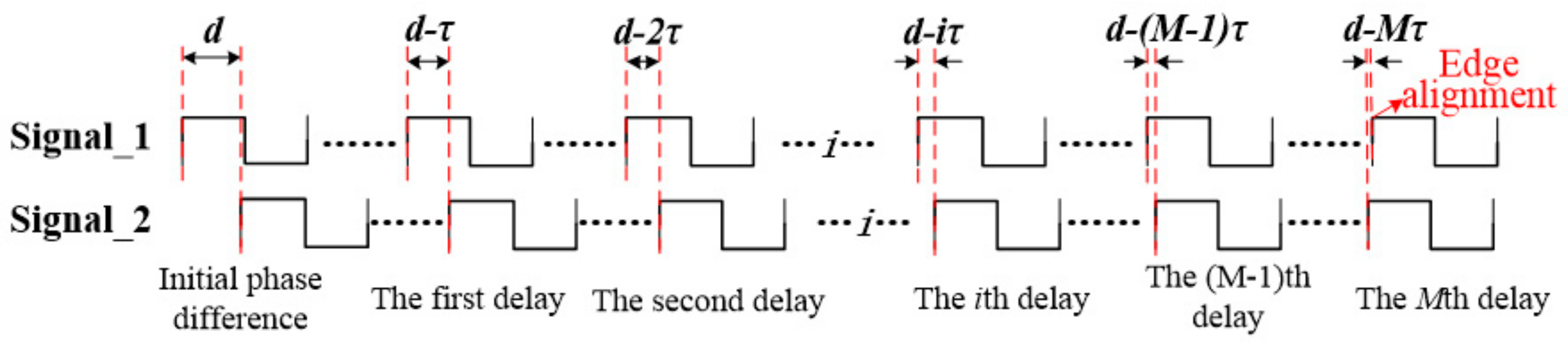
The phase difference between two periodic signals with the same frequency can be calculated by time difference. Progressive phase shift (PPS) utilizes delay accumulation to quantify the time difference, as shown in
Figure 1. In the figure,
d is the phase difference between Signal_1 and Signal_2. The rising edges of the two signals are detected by the phase detection circuit. When the signals are not aligned, Signal_1 is delayed by
τ until edge alignment of the two signals is detected. If the edge alignment is detected after m delays of
τ have been performed. Then the measurement result of the phase difference can be obtained from the Equation (1).
Though the principle of PPS is simple, difficulties exist in the implementation of the method. The first difficulty is that we must minimize the step delay (τ) to improve the measurement precision. Second, the delay linearity of the delay elements determines the measurement error of the method. A commonly used method to implement PPS is constructing a delay line. Delay lines can be constructed by digital or analog elements. However, analog circuits usually suffer from large area and poor environment stability. Hence, this paper uses digital circuits to construct the delay line.
Excited by the continuous development in CMOS technology, FPGA devices have become very popular for rapid system prototyping, logic emulation and reconfigurable computing because of their lower manufacturing cost and shorter development time. In the FPGA chip, flip flops, buffers and carry logics are usually used to realize signal delay [
14]. However, the delay elements listed above are not easily controlled and the measurement range is limited because of the relatively large size at the state of being cascaded.
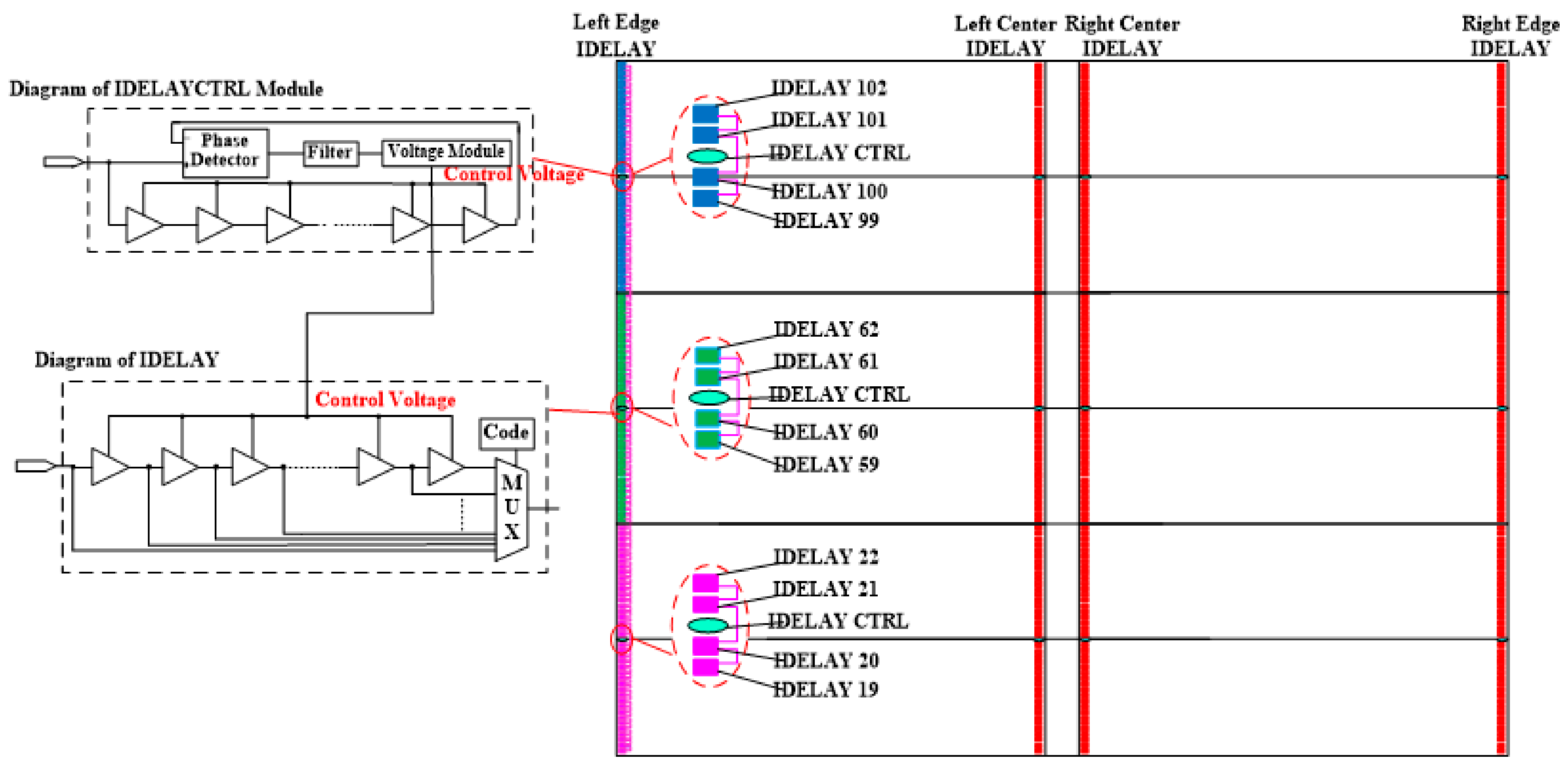
Many FPGA devices contain programmable delay elements in the I/O logic resources, which can provide adjustable and fine-resolution delay. The programmable delay elements can be used to realize the phase difference measurement method based on PPS. The programmable delay elements are programmable tap delay lines. In the Xilinx Virtex series FPGA chips, the primitive of the programmable delay element is IDELAY [
15,
16]. There are 64 delay taps in an IDELAY, and the tap delay is calibrated by the reference clock. The schematic diagram of the IDELAY is shown in
Figure 2. The delay taps are voltage controlled delay elements, which are calibrated from the IDELAY control (IDELAYCTRL) module. The IDELAYCTRL module continuously calibrates the individual delay taps in its region, to reduce the effects of process, voltage, and temperature (PVT) variations. The IDELAYCTRL automatically changes the time delay over voltage and temperature to ensure the tap delays remain at the requested time. The individual tap delay of the IDELAY is determined by the frequency of the reference clock, which is calculated from (2). For the frequency of the reference clock, values from 190 MHz~210 MHz or 290 MHz~310 MHz are allowed, then the tap delay can be within the range of 75~82 ps or 50~54 ps. Hence, the resolution of the phase difference measurement can be 50 ps, and the measurement range of a single IDELAY is 3.2 ns.
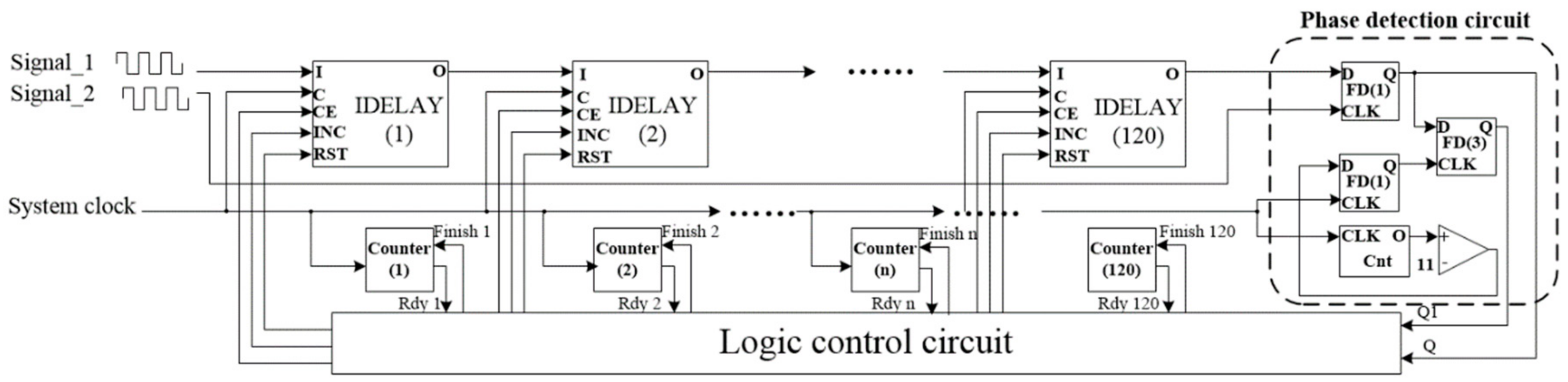
To enlarge the measurement range, IDELAYs are cascaded into programmable delay lines (PDL). The structure of the design is shown in
Figure 3. A total of 120 IDELAYs are cascaded into a line to delay Signal_1, tap by tap, which is controlled by the logic control circuit. An IDELAYCTRL module calibrates 40 IDELAY modules within its clock region, which is shown in
Figure 2. The INC signal increases the number of taps to delay Signal_1, while CE enables the increase. The Rdy signal is used to judge whether the counter is full, and the Finish signal is used to enable and disable the counter. When the counter is full or edge alignment is detected, the Finish signal disables the counter and holds its value.
In the phase detection circuit, D flip-flops are used. However, if the setup and hold time of flip-flops are not satisfied, the flip-flop is into metastable state. The flip-flop can return to stable state from metastable state after a certain delay. Therefore, in the phase detection circuit, three D flip-flops are employed to generate the trigger of edge alignment, which is two clock periods later than the time of edge alignment and can eliminate the influence of metastable state to the system.
According to the architecture of the delay line, the delay linearity of delay elements is of great importance, which directly influences the measurement error. Poor linearity results in large measurement error. In this design, IDELAY’s tap delay provides an extraordinary linearity for the delay line because it is driven by an external fixed-frequency reference clock and uses a feed-back structure to calibrate the delay of each tap, which reduces and compensates for the influence of process, voltage and temperature (PVT) variations. Therefore, when the frequency of the reference clock is specified, the tap delay is with excellent delay linearity. The minimum delay a PDL can provide is 50 ps under 310 MHz. Then, the measurement error (
ε) caused by edge alignment can be obtained by Equation (3).
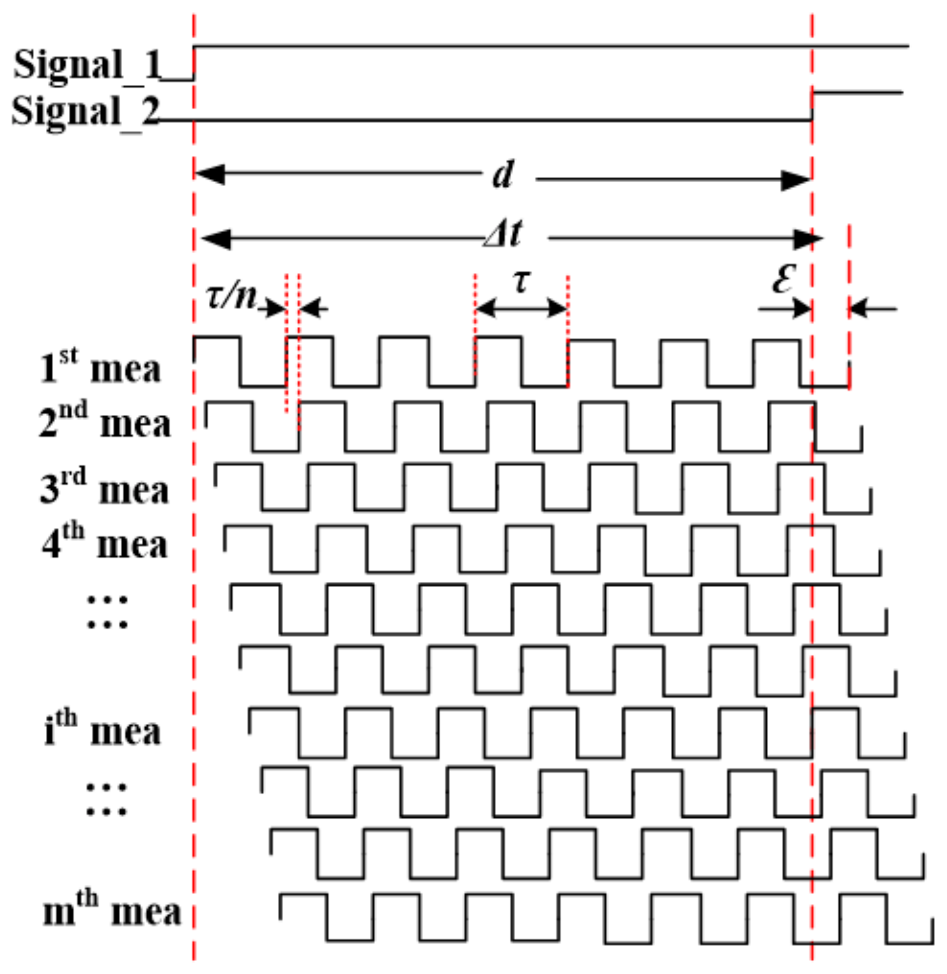
3. Principle of Double Progressive Phase Shift
According to the structure of the IDLEAY module, a relatively programmable delay is featured, and it has the ability of offering a tap delay in the range of 75~82 ps or 50~54 ps. Only a 50 ps tap delay is used in the method above. Hence, we consider whether other delays can be incorporated to improve the measurement resolution.
To improve the resolution, a modified method is introduced, which conducts multiple measurements. The timing diagram of the modified method is shown in
Figure 4. The first measurement is carried out using the method described above. The second measurement is performed after Signal_1 has been delayed by
τ/
n, which means the phase difference is decreased by
τ/
n. Similarly, the third measurement is performed after Signal_1 has been delayed by 2
τ/
n. Measurements are performed n times in total. Therefore, the measurement result and measurement error can be calculated from Equations (3) and (4), where
Δti and
εi represents the measurement result and measurement error of the
ith time, respectively, and
εi satisfies 0 ≤
εi <
τ. The first measurement error is marked as
ε1, and the second measurement error
ε2 can be calculated from (4). In (4),
represents a real remainder operation and the return value is the remainder of
x/
y. Hence, it can be concluded that the measurement error
εi can be calculated from (5), and the measurement error ε can be calculated from (6)–(8).
It is easy to find that
is an arithmetic sequence with a common difference of
by sorting the values from small to large. The minimum value of the sequence is
. According to the summation formula of the arithmetic sequence, the sum of the sequence is less than
. Equation (8) is reduced to a simpler form as shown in Equation (9), which can be simplified as
.
Equation (9) proves that the modified method is an effective way to reduce the measurement error. Taking PDL’s delay characteristic into account, the 50 ps tap delay and the 75 ps tap delay can be used to realize a double PPS phase measurement method. When
τ is 50 ps, an initial 75 ps delay for Signal_1 has the same effect with 25 ps in the second measurement. Then, the measurement error is reduced to
τ/2 or 25 ps. Thus the measurement result of the double PPS can be obtained from Equation (10).
Then, two measurements should be performed to obtain
Δt1 and
Δt2. The logic control circuit calculates
Δtj (
j = 1, 2) according to Equation (11), where
λ1 and
λ2 represent the the initial state of the D flip-flops and the phase detection result, respectively. In Equation (11), M is the number of PDLs Signal_1 has passed through, m is the number of active taps in the
Mth IDELAY,
ci is the number of taps in the first M-1 IDELAYs, and
T is the period of the measured signal.
5. Conclusions
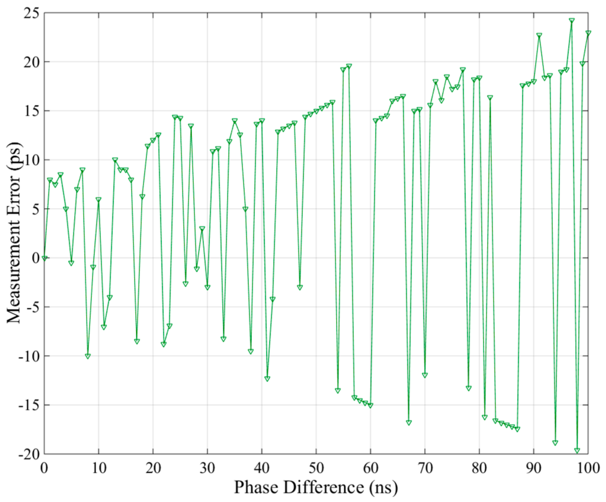
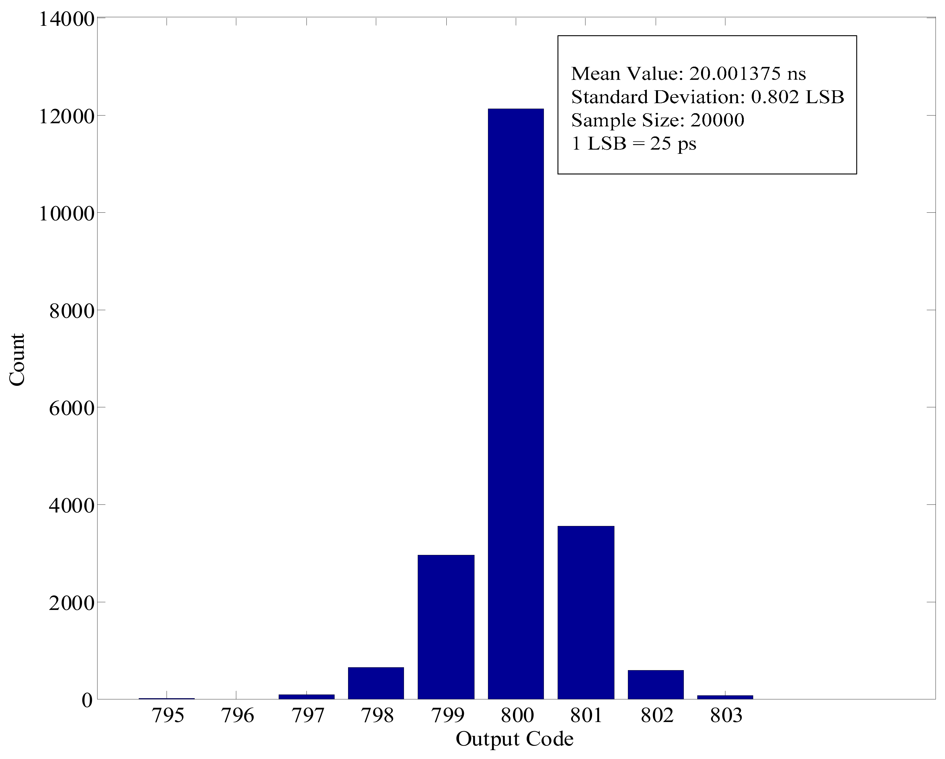
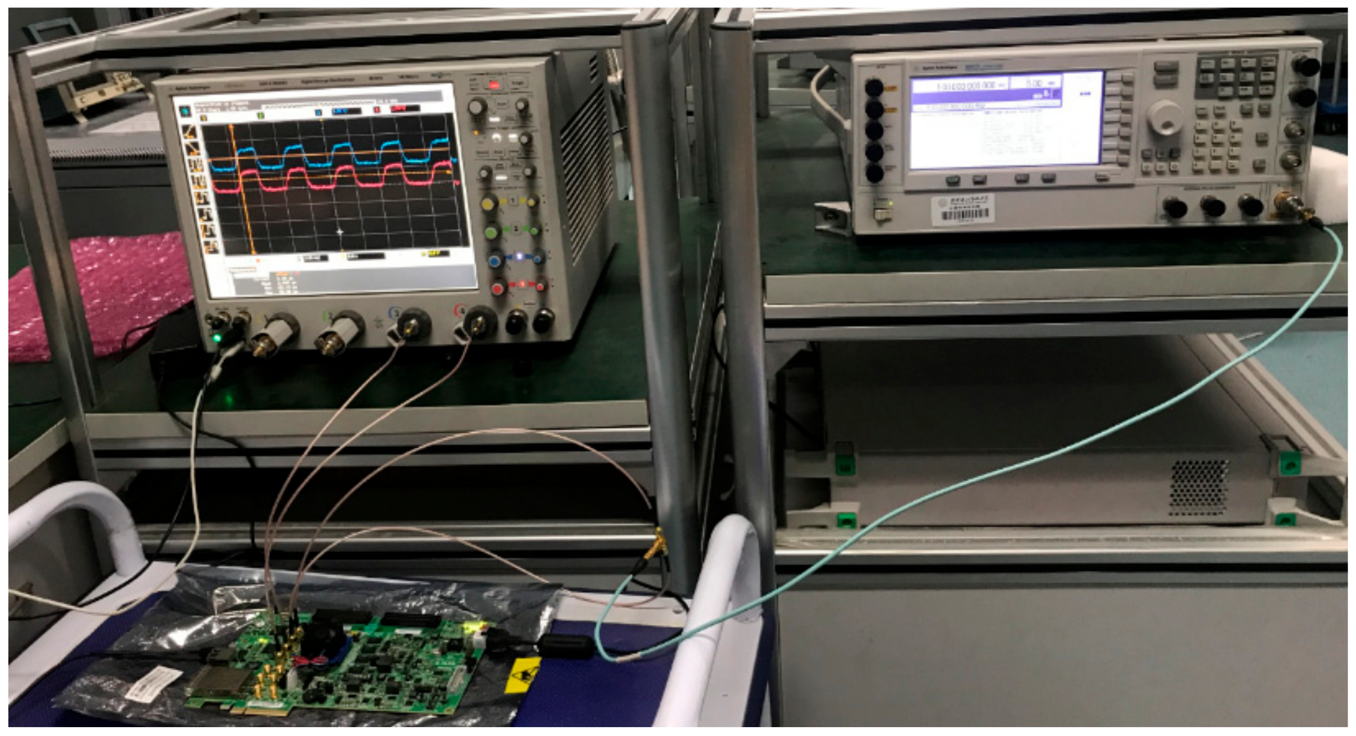
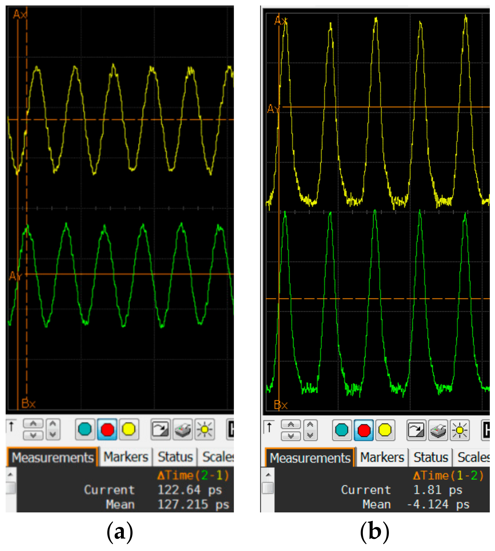
This paper proposed and tested a phase difference measurement method between two periodic signals based on the principle of PPS. A double PPS method is further proposed to improve the resolution and reduce measurement error. As a result of the double PPS structure, the resolution is improved to 25 ps. To further improve the resolution, the proposed method is implemented on the latest FPGA platform. The implementation on Xilinx KCU105 evaluation board obtains resolution of 2.5 ps, and the measurement error is within the range of ±5 ps.
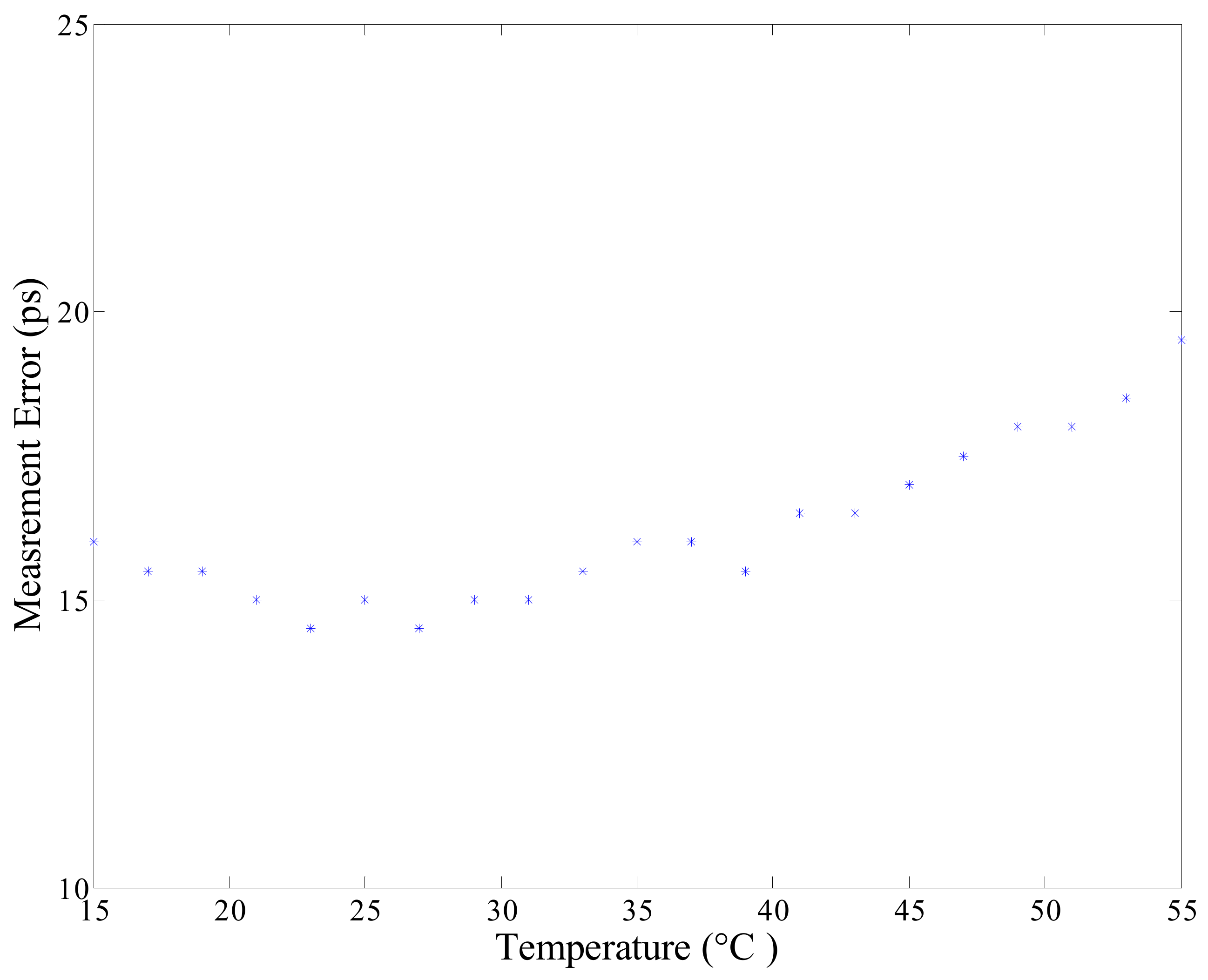
The proposed method is implemented in a single FPGA chip, which features high integration density and short development time. Another advantage of the proposed method is that it offers a high measurement rate, which profits from the principle of the method algorithm and does not require complicated calculations. The longest time needed for the measurement is less than 0.1 µs. Moreover, experimental results indicate that the proposed method provides good PVT stability.


