Article

Solution-Processable ZnO Thin Film Memristive Device for Resistive Random Access Memory Application

1
Computational Electronics and Nanoscience Research Laboratory, School of Nanoscience and Biotechnology, Shivaji University, Kolhapur 416004, India
2
School of Electronics Engineering, Chungbuk National University, Cheongju 28644, Korea
*
Authors to whom correspondence should be addressed.
Authors contributed equally to this manuscript.
Electronics 2018, 7(12), 445; https://doi.org/10.3390/electronics7120445
Submission received: 1 November 2018 / Revised: 4 December 2018 / Accepted: 13 December 2018 / Published: 17 December 2018
(This article belongs to the Section Microelectronics)

Abstract

:
The memristive device is a fourth fundamental circuit element with inherent memory, nonlinearity, and passivity properties. Herein, we report on a cost-effective and rapidly produced ZnO thin film memristive device using the doctor blade method. The active layer of the developed device (ZnO) was composed of compact microrods. Furthermore, ZnO microrods were well spread horizontally and covered the entire surface of the fluorine-doped tin oxide substrate. X-ray diffraction (XRD) results confirmed that the synthesized ZnO was oriented along the c-axis and possessed a hexagonal crystal structure. The device showed bipolar resistive switching characteristics and required a very low resistive switching voltage (±0.8 V) for its operation. Two distinct and well-resolved resistance states with a remarkable 103 memory window were achieved at 0.2-V read voltage. The developed device switched successfully in consecutive 102 switching cycles and was stable over 102 seconds without any observable degradation in the resistive switching states. In addition to this, the charge–magnetic flux curve was observed to be a single-valued function at a higher magnitude of the flux and became double valued at a lower magnitude of the flux. The conduction mechanism of the ZnO thin film memristive device followed the space charge limited current, and resistive switching was due to the filamentary resistive switching effect.

Graphical Abstract

1. Introduction

Memristor/memristive devices are popular in academia as well as in industry due to their simple structure, zero power requirement for sustaining resistive states, and high speed of operation [1]. These devices can be used as a basic building block for neuromorphic computing [2,3], nonvolatile memory [4,5], and signal processing applications [6,7]. They were theoretically predicted by Leon Chua as a fourth basic circuit element in 1971 [8] and were experimentally realized by a team of Hewlett Packard researchers in 2008 [9]. Pinched hysteresis loops in the current–voltage (I–V) plane and single-valued charge–magnetic flux (q–φ) relations are some of the defining characteristics of the memristor device and can be experimentally realized by properly engineering the active material.
A literature survey suggested that different kinds of materials could be used for the development of memristive devices. The transition metal oxides [10], perovskite oxides [11], chalcogenides [12], and organic compounds [13] are some of the materials that show resistive switching behavior. Among them, metal-oxides including ZnO [14,15], NiO [16], TiO2 [17,18], and WO3 [19] are promising materials because of their low power consumption, multistate resistive switching characteristics, and simple chemical composition. Out of these materials, ZnO is a versatile material for technological applications. It is a wide band gap semiconducting material and has attracted much attention due to its excellent optical, electrical, and piezoelectric properties [20]. At room temperature, the electron hall mobility of ZnO single crystals is in the order of 200 cm2/Vs and they also show large exciton binding energy (around 60 meV) [21]. In recent years, bipolar resistive-switching-based memristive devices have been developed using different physical and chemical techniques. Recently, Gul et al. developed a sputter-deposited ZnO memristive device and demonstrated its bipolar resistive switching characteristics in a Al/ZnO/Al-based memristive device [22]. A bipolar resistive-switching-based memristive device with a low operating voltage (±0.88 V) was developed by Dongale et al. They studied the effect of temperature on the developed device using a thermal reaction model [15]. Choi et al. fabricated a reliable and cost-effective ZnO memristive device using an electrohydrodynamic printing technique. The device required 1.6 V/−2 V operating voltage and provided an on/off ratio in the order of ~10:1 [23]. Many reports suggest that a ZnO-based memristive device can be useful for memory and neuromorphic computing applications [24,25]. However, very few reports are available that consider a low-cost fabrication methodology for ZnO memristive devices [23,26,27,28]. In addition to this, the ZnO memristive devices reported in the existing literature require a higher resistive switching voltage (VSET and VRESET > 1 V), and very few reports demonstrate the charge–magnetic flux characteristics.
In the present work, we investigated the simplest way to fabricate a bipolar resistive-switching-based Ag/ZnO/Fluorine-doped tin oxide (FTO) thin film memristive device using the doctor blade method. Morphological, structural, and electrical characterizations of the ZnO thin film memristive device were carried out using scanning electron microscopy (SEM), X-ray diffraction (XRD), and a memristor characterization platform, respectively. The developed device showed the fingerprint pinched hysteresis loop in the I–V plane with a low resistive switching voltage (±0.80 V). An excellent 103 memory window with stable nonvolatile memory (endurance and retention) properties was achieved at a 0.2-V read voltage. The time domain flux, time domain charge, charge–magnetic flux, and charge–voltage characteristics of the ZnO thin film memristive device were also determined. The excellent electrical results and fabrication-friendly procedure of the present work could help to develop cost-effective and rapidly produced devices for nonvolatile memory applications.

2. Experimental Details

2.1. Materials and Method

All the reagents used for synthesis were of analytical grade and were used without further purification. Zinc acetate (SD-fine, Mumbai, India) and ammonia (SD-fine, Mumbai, India) were used for the synthesis of ZnO powder, whereas ethyl cellulose (SD-fine, Mumbai, India), lauric acid (Himedia, Mumbai, India), terpineol (Loba chemie, Mumbai, India), and ethanol (SD-fine, Mumbai, India) were used for the thin film development (doctor blade method). The FTO coated on a glass substrate (10 Ω/sq.) was used as a bottom electrode. The FTO substrates were cleaned with laboline and distilled water and were finally rinsed with acetone. The doctor blade technique was used for the development of the ZnO active layer on the FTO substrate.

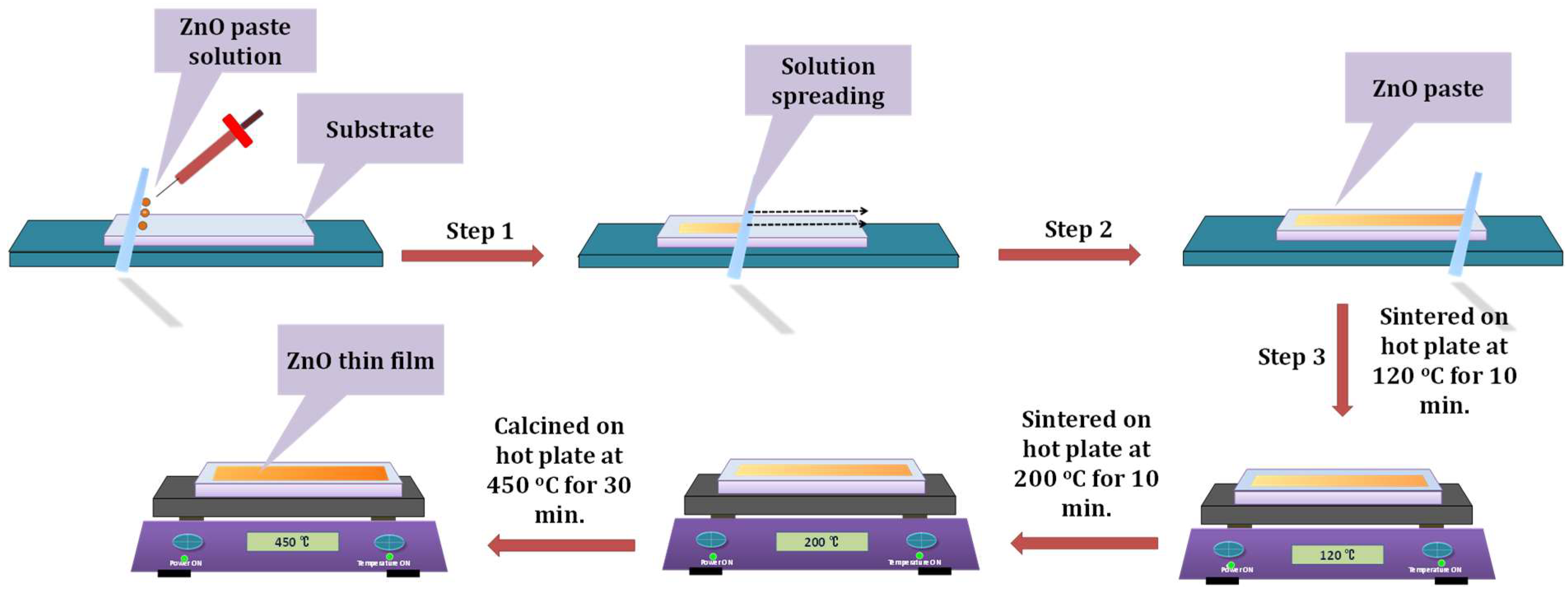
2.2. Synthesis of ZnO Powder and Development of ZnO Thin Film Using the Doctor Blade Method

Figure 1 depicts the schematic representation of the ZnO powder synthesis procedure. In the typical process, 0.1 M zinc acetate (C4H6O4Zn·2H2O) solution was prepared in 50 mL of double-distilled water (DDW). This solution was kept on a magnetic stirrer until it became homogeneous and clear, after which ammonia (NH3) was added dropwise with continuous stirring. After the addition of a few milliliters of NH3, the solution initially became precipitated and then colorless. The resultant system was transferred to a stainless-steel autoclave and hydrothermally treated at 80 °C for 1 h. After completion of the reaction, the resultant system was allowed to cool down to room temperature. The synthesized powder was washed two times with ethanol and distilled water and then air-dried at room temperature for 2 h. Finally, the as-synthesized ZnO powder was annealed at 350 °C for 1 h. Figure 2 shows the schematic representation of the doctor blade deposition technique for the development of the ZnO thin film. In this technique, ZnO powder (1 g) was blended with a mixture of ethyl cellulose (0.3 g) and lauric acid (0.1 g) in a mortar under vigorous grinding with a pestle, to which five to six drops of terpineol was added. During grinding, a few drops of alcohol were added in order to reduce viscosity and mix the precursors properly. This mixture was blended for 1 h to obtain a uniform and lump-free paste. The prepared paste was coated on a conducting side of a precleaned FTO substrate. This substrate was sintered at 120 °C for 10 min, 200 °C for 10 min, and then calcined at 450 °C for 30 min to remove the binder.

2.3. Development and Characterizations of ZnO Memristive Device

In the present investigation, Ag acted as a top electrode, ZnO as an active layer, and FTO as a bottom electrode. The active memristive layer (ZnO) was coated on the FTO substrate using the doctor blade method. The Ag was patterned on the ZnO layer so as to work as a top electrode for the memristive device. The Ag layer (~500 nm) was patterned using a thermal evaporation system (Vacuum Techniques, Model – VT-ACG-03, Bengaluru, India). In this experiment, Ag evaporation slugs (Sigma-Aldrich, Mumbai, India) were kept in the evaporation boat and a 10−5-Torr vacuum environment was created. This resulted in a good-quality top Ag contact for electrical measurements. The synthesized ZnO thin films were characterized by morphological, structural, and electrical characterization techniques. The surface morphology of the ZnO thin film was investigated using SEM (JEOL-JSM 6360 A, Japan). The phase and crystal structures of the ZnO thin film were examined using XRD with CuKα λ = 1.5406 Å (Bruker Model D2 phaser, United States). The electrical measurements of the Ag/ZnO/FTO thin film were recorded using an electrochemical workstation (Autolab N-Series) and memristor characterization platform (ArC ONE). During all electrical measurements, we biased the top Ag electrode with respect to bottom FTO electrode. The endurance and retention measurements were obtained with the help of a pulsed measurement protocol. The time domain flux, charge, charge–magnetic flux, and charge–voltage characteristics were calculated using experimental I–V data by employing Equations (2)–(6), which are shown in the next section.

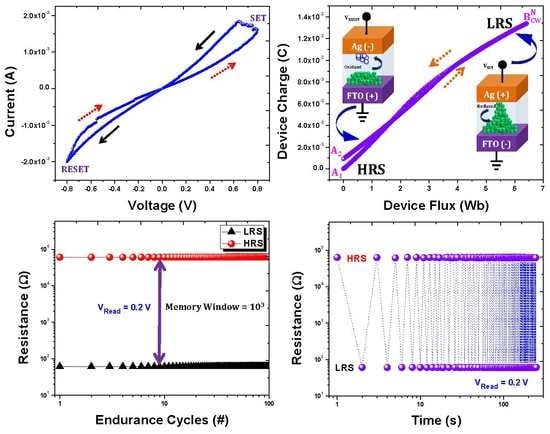
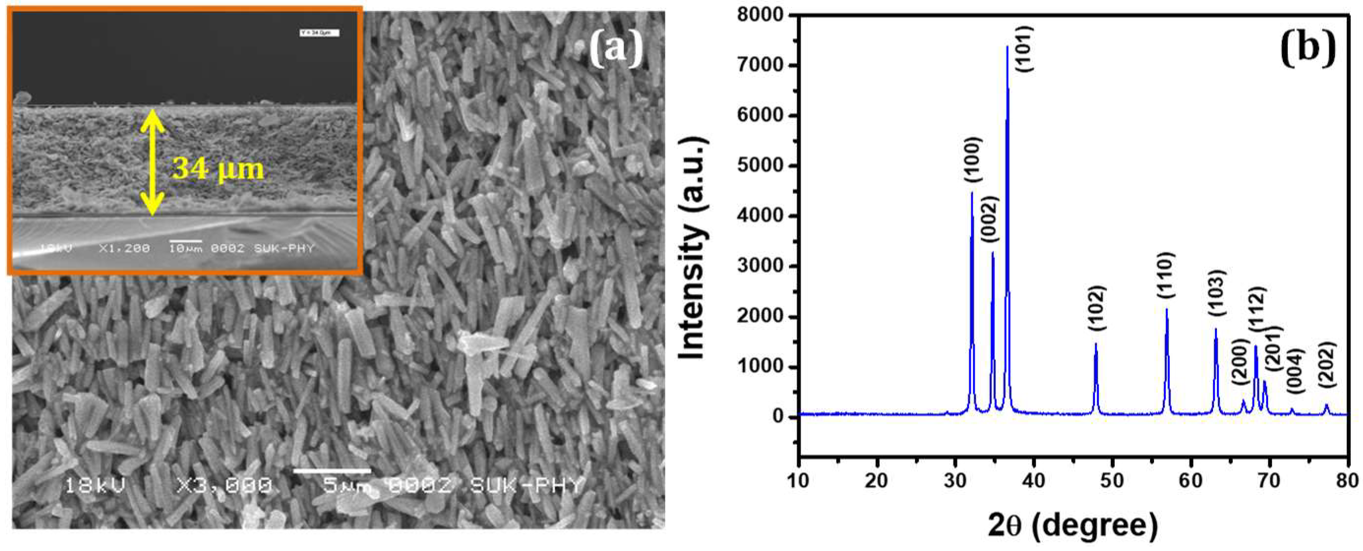
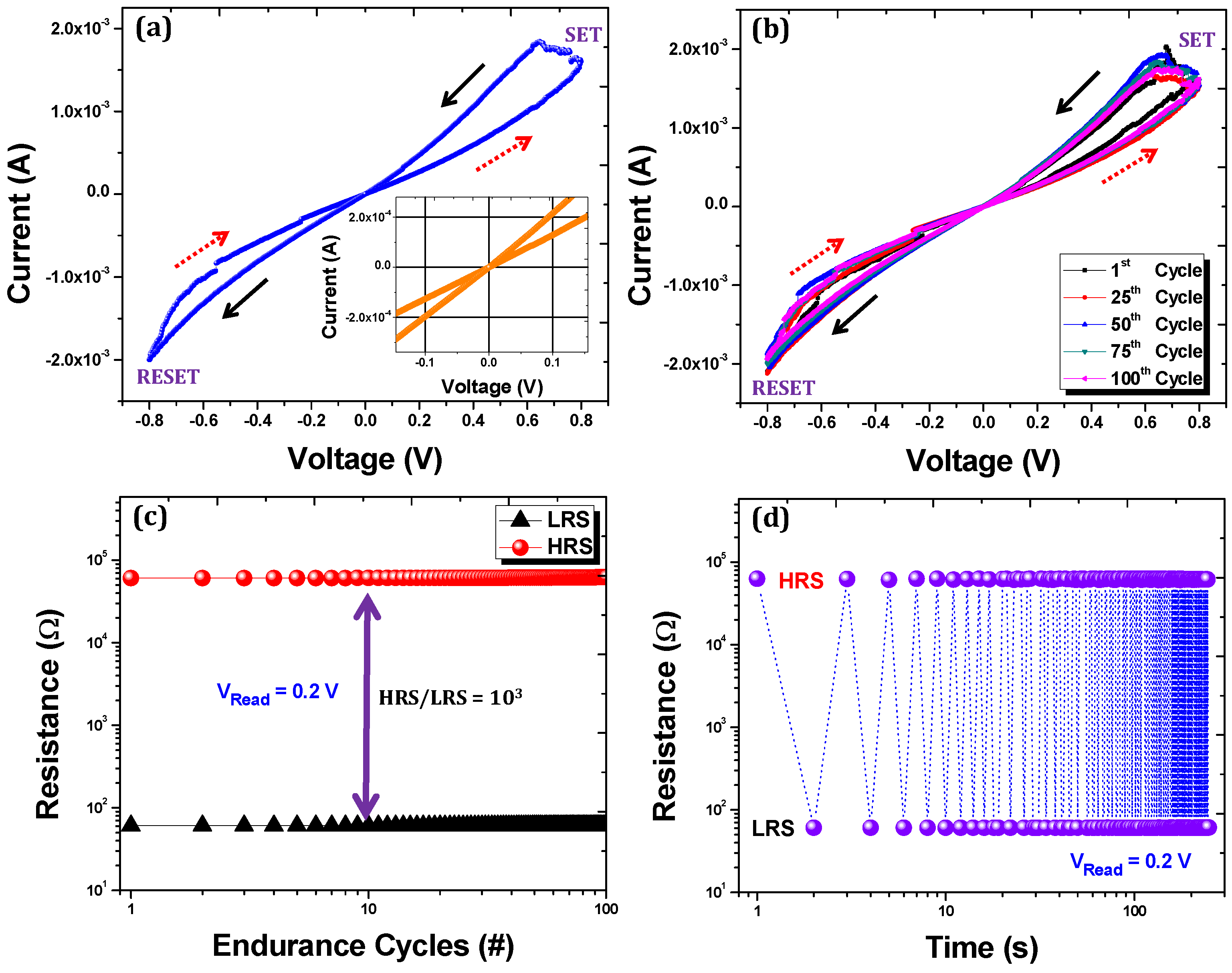
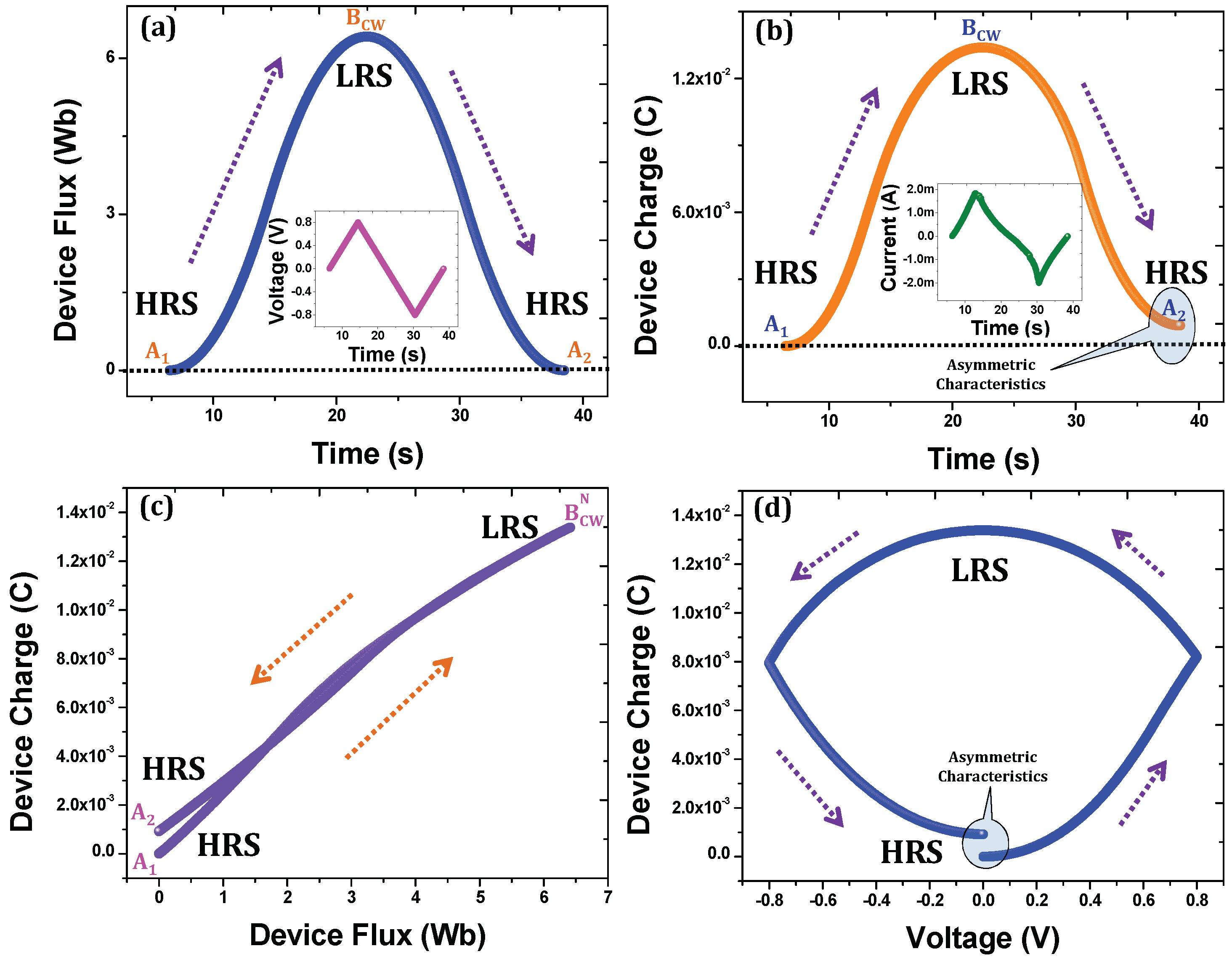
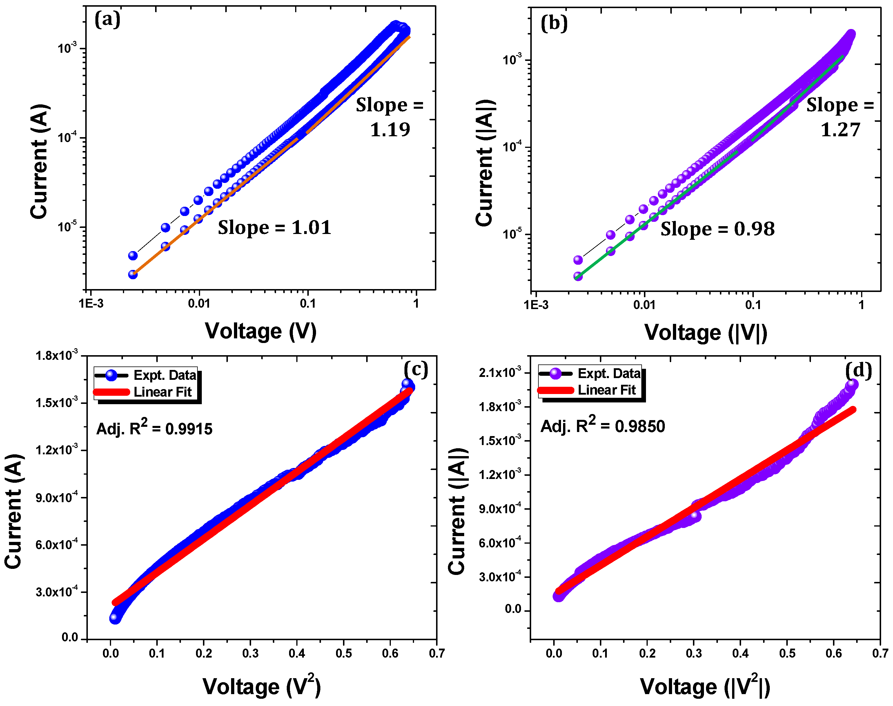
3. Results and Discussions

The scanning electron micrograph of the ZnO thin film is shown in Figure 3a. The surface micrographs suggested that the ZnO thin film was composed of compact microrods. Furthermore, ZnO microrods were well spread horizontally and covered the entire surface FTO substrate. The cross-sectional SEM image of the ZnO thin film is shown in the inset of Figure 3a. The thickness of the thin film was found to be 34 µm. The cross-sectional image suggested that the uniform deposition of ZnO was obtained by the doctor blade method. ZnO is an II–VI binary compound semiconductor that has a cubic zinc-blende or hexagonal wurtzite crystal structure where each anion is wrapped by four cations at the corners of the tetrahedron. This tetrahedral coordination has substantial ionic behavior with sp3 covalent bonding. The ionicity of ZnO resides at the borderline between a covalent and ionic semiconductor. Figure 3b shows the XRD pattern of the ZnO powder sample. XRD results suggested that the prepared ZnO sample was nanocrystalline in nature and matched well with the hexagonal (wurtzite) crystal structure (JCPDS No.–36-1451). The large broadening of the ZnO peaks was due to the very small crystallite size. The major peaks (i.e., (100), (002), and (101)) confirm the hexagonal (wurtzite) crystal structure. Some other Bragg’s peaks, such as (102), (110), (103), (200), (112), (201), (004), and (202), were also observed with relatively lower intensities. The average crystallite size (D) was calculated from the XRD pattern by using Scherer’s relation, as given in Equation (1):
D = 0.9 λ β c o s θ
where D is the crystallite size, λ is the wavelength of X-ray (1.5406 Å), β is the fullwidth at half-maxima, and θ is the angle of diffraction. The average crystallite size of the prepared ZnO sample was found to be 62 nm, which confirmed the nanocrystalline nature of ZnO. The lattice parameters of the prepared ZnO sample were a = b = 3.2548 Å and c = 5.2052 Å. In a nutshell, the XRD results confirmed that the synthesized ZnO sample was oriented along the c-axis and possessed a hexagonal crystal structure.
The ideal memristor device is a passive circuit element with inherent memory and nonlinearity properties. The extended class of memristor device, popularly known as the memristive device, is more practical and suitable for a wide range of applications. The memristive device is generally recognized by a pinched hysteresis loop in the I–V plane and one such I–V characteristic of the Ag/ZnO/FTO thin film device is shown in Figure 4a. The inset shown in Figure 4a represents the zero crossing property of the memristive device. The fingerprint pinched hysteresis loop was clearly observed for the Ag/ZnO/FTO thin film device, which suggested that the developed device acted as a memristive device. In order to obtain the pinched hysteresis loop in the I–V plane, the voltage swept from 0 to +0.8 V, +0.8 to 0 V, 0 to −0.8 V, and −0.8 to 0 V. Initially, the device was in the high-resistance state (HRS) at 0 V. The current (I) of the device increased as the sweep voltage increased from 0 to 0.8 V. At 0.8 V, the device started to change its resistive switching state. This is the ON state, or low-resistance state (LRS), of the device and the corresponding voltage is known as the SET voltage. This state made uninterrupted progress up to −0.8 V. After −0.8 V, the device again started to change its resistive switching state, and the corresponding voltage is known as the RESET voltage. For a clear understanding, the continuous arrows represent the LRS of the device, whereas the dotted arrows represent the HRS of the device. In order to test the repeatability of the measurements, we measured the I–V characteristics for 100 consecutive cycles, as shown in Figure 4b. The results suggested that the Ag/ZnO/FTO thin film memristive device possessed reliability and repeatability in the measurements.
The memory property of the memristive device is described by memristance (M). It is divided into two resistance states, namely, LRS and HRS. Furthermore, the transition between two resistance states dictates the application domain of the memristive device. An abrupt transition from HRS to LRS and vice versa is useful for resistive switching memory applications, whereas a smooth transition of resistive switching states is useful for neuromorphic computing applications. The endurance and retention characteristics of the Ag/ZnO/FTO thin film memristive device are shown in Figure 4c,d, respectively. For the nonvolatile memory measurements, the pulsed and nondisruptive memory measurement protocol was used. In the typical measurement, a series of write pulses with of ±0.8-V magnitude were applied and the resistance of the device was measured with a 0.2-V read pulse. Throughout the measurement, a 300-µs pulse duration was maintained for write and read pulses. Two distinct and well-resolved resistance states with a remarkably higher memory window (HRS/LRS) were observed for the developed device. In the present work, we achieved a 103 memory window at a 0.2-V read voltage. Such a higher memory window is required for resistive random access memory applications [29,30,31]. The endurance property could be used to probe the cycle-to-cycle resistive switching behavior of the memory device. In the present case, the developed device switched successfully in consecutive 102 switching cycles. The stability of LRS and HRS states were studied using a retention test. It was observed that the LRS and HRS were stable over 102 s without any observable degradation in the resistance states.
The ideal memristor can be recognized by the charge–magnetic flux (q–φ) relation and pinched hysteresis loop in the I–V plane. The mathematical formulation of the memristor suggested that the q–φ characteristics must be a nonlinear, continuously differentiable, and monotonically increasing single-valued function [8]. In view of this, memristor devices can be defined as the basis of a charge and magnetic flux relation, such that [32]
f M ( φ , q ) = 0 o r φ = f ( q ) o r q = g ( φ ) o r d φ d q = M .
The voltage (v) across or current (i) through the memristor can be obtained by differentiating Equation (1) w.r.t. ‘t’, [32]:
v = M(q)i
i = W(φ)v
where, v = d φ d t and i = d q d t . Equation (3) is a current-controlled memristor, whereas Equation (4) is known as a voltage-controlled device. In this case, the q and φ act as state variables, whereas M(q) and W(φ) are known as memristance and memductance, respectively. In the present case, we applied external voltage and measured the current of the device. In classical terms, we controlled the memristance of the device by the instantaneous time integral of the current. Therefore, the developed Ag/ZnO/FTO thin film device acted as a current-controlled memristive device. In order to investigate the basic flux and charge characteristics, we used Equations (5) and (6) and experimental I–V data (time-dependent) [33]:
q ( t ) = t i ( t ) d t
φ ( t ) =   t v ( t ) d t
The time domain flux and charge characteristics of the Ag/ZnO/FTO thin film memristive device are shown in Figure 5a,b. The external voltage stimulus and current response are shown in the inset of Figure 5a,b, respectively. The initial (A1), half-period (BCW), final-period (A2), and turning ( B CW N ) points represent the resistive switching states of the memristive device. The device was in the HRS at the initial and final-period points and went into the LRS at half-period points. The obvious symmetric time domain flux characteristics were observed for the developed device. This was due to fact that the voltage stimulus was symmetric in nature and its integration ( φ ( t ) ) had to be a symmetric function. However, the time domain charge characteristics were found to be asymmetric in nature (final charge value). This kind of asymmetric behavior suggested that the pinched hysteresis loop of the developed device was asymmetric in nature. In addition to this, the shape of the time domain charge characteristics was asymmetric in nature. This kind of asymmetric behavior (final charge value and shape) led to double-valued q–φ characteristics which were the opposite of the definition of the ideal memristor device [8]. One such characteristic is shown in Figure 5c. It is worth mentioning that the turning ( B CW N ) and final-period (A2) points dictate the nature of the q–φ characteristics. In the present case, the single-valued q–φ curve was observed at the LRS and became double valued at the HRS. The double-valued q–φ curve at the HRS was due to the incomplete breaking of the conductive filament and some sort of parasitic capacitance or inductance present in the device [34]. In addition to this, the asymmetric nature of the device can be represented with the help of charge–voltage characteristics, as shown in Figure 5d. The transition of the HRS to LRS and vice versa and the asymmetric nature are clearly observed from the charge–voltage characteristics. This kind of novel representation is useful for the identification of the ideal memristor device from nonideal memristor devices.
The conduction mechanism of the Ag/ZnO/FTO memristive device was obtained by plotting the I–V characteristics on a log–log scale. Figure 6a,b represents the double logarithmic I–V characteristics of the ZnO memristive device in positive and negative bias, respectively. The slopes of the low-voltage range (0 to ±0.1 V) and high-voltage range (±0.1 to ±0.8 V) were calculated and are depicted in the Figure 6a,b. For the low-voltage range, the slope was ~1 in both bias regions. This suggested that the current of the device was directly proportional to the applied voltage, which confirmed that the Ohmic conduction mechanism was dominated in the low-voltage range. The current of the device increased suddenly in the high-voltage range and, therefore, the magnitude of the slopes also increased in both bias regions. In order to investigate the conduction mechanism of the high-voltage range, the Child’s law characteristics were plotted, as shown in Figure 6c,d. Child’s law was well fitted to the experimental data, with the adjusted R2 equal to 0.9915 and 0.9850 for positive and negative bias data. This indicated that Child’s law dominated in the high-voltage range. It is a well-known fact that the space charge limited current (SCLC) conduction mechanism appears with the Ohmic conduction mechanism at the low-voltage range and Child’s law at the high-voltage range. In a nutshell, the SCLC conduction mechanism was responsible for the charge transport of the Ag/ZnO/FTO memristive device.
The electrical results showed the abrupt increase in the current at the SET and RESET voltage point. Furthermore, two distinct and well-resolved resistance states were observed during nonvolatile memory measurements. In general, this kind of result was observed only when the filamentary type of resistive switching effect dominated in the memristive device. Considering the electrical characteristics of the Ag/ZnO/FTO thin film memristive device, the possible filamentary type resistive switching mechanism is shown in Figure 7. In the present case, Ag acted as a top electrode. It is a well-known fact that a Ag electrode work as an electrochemically active component in filament formation and the rupture process [35]. When a positive voltage was applied to the top Ag electrode with respect to the bottom FTO electrode, oxidation of Ag occurred and Ag+ cations were generated (Ag → Ag+ + e). These cations traveled through the active ZnO layer and reduced at the bottom FTO electrode (Ag+ + e → Ag). The precipitations of Ag metal atoms at the bottom FTO electrode resulted in the growth of Ag filament in the ZnO layer. This metal filament finally ended at the top electrode, as shown in Figure 7a. The fully grown conductive filament helped to switch the device to the ON or LRS state. In the next case, an electrochemical dissolution of Ag took place due to the change in the polarity of the applied voltage. This change in the polarity ruptured the conductive filament and drove the device into the OFF or HRS state. In a nutshell, the formation and rupture of the conductive filament gave rise to the bipolar resistive switching effect in the Ag/ZnO/FTO thin film memristive device.
The performance comparison of ZnO memristive device with existing ZnO-related solution-processable memory devices is summarized in Table 1. These results indicate that our solution-processable ZnO memristive device is a good candidate for nonvolatile resistive memory applications.

4. Conclusions

In conclusion, we have developed a filamentary resistive-switching-based ZnO thin film memristive device using the doctor blade method. The surface micrographs suggested that the ZnO thin film was composed of compact microrods. The microrods spread horizontally and covered the entire surface of the FTO substrate. XRD results confirmed that the synthesized ZnO sample was oriented along the c-axis and possessed a hexagonal crystal structure. The fingerprint pinched hysteresis loop was clearly observed for the Ag/ZnO/FTO thin film device, which suggested that the developed device acted as a memristive device. A remarkably low resistive switching voltage (±0.8 V) with a 103 memory window was achieved for the developed device. The nonvolatile memory properties, such as endurance and retention, suggested that the device switched successfully in consecutive 102 switching cycles and was stable over 102 seconds without any observable degradation in the resistive switching states. The ideal memristor can be recognized by the single-valued q–φ curve. In the present case, the q–φ curve was observed to be a single-valued function at a higher magnitude of the flux (or at LRS) and became double valued at a lower magnitude of the flux (or at HRS). The double-valued q–φ curve at the HRS was due to the incomplete breaking of the conductive filament and some sort of parasitic capacitance or inductance present in the device. These results suggest that the developed device is an extended class of memristor device or, more specifically, it is a memristive device. The conduction mechanism investigations suggest that the SCLC conduction mechanism dominated and the bipolar resistive switching effect was due to the formation and rupture of the metallic conductive filament.

Author Contributions

Authors T.D.D, S.K. and A.D.S. conceptualized the idea. S.R.P., M.Y.P. and T.D.R. performed the synthesis. S.S.K., A.A.P., O.S.B. and S.D.J. did the characterizations. S.R.P., M.Y.P. and T.D.R. performed the electrical measurements. T.D.D., S.K. and A.D.S. analyzed the data. S.R.P., M.Y.P. and T.D.R. wrote the first draft and T.D.D., S.K. and A.D.S. finalized the manuscript. All authors reviewed the manuscript. All authors read and approved the final manuscript.

Funding

The author T. D. D. thanks Shivaji University, Kolhapur for the financial assistance under the “Research Initiation Scheme”. A. D. S. thanks the Department of Science and Technology (DST), Ministry of Science and Technology, Government of India, New Delhi for the INSPIRE faculty research grant (Award No. DST/INSPIRE/04/2015/002601). This work was supported by a grant from the National Research Foundation of Korea (NRF), funded by the Korea government (MSIP) (2018R1C1B5046454).

Conflicts of Interest

The authors declare no conflict of interest.

References

  1. Salaoru, I.; Khiat, A.; Li, Q.; Berdan, R.; Prodromakis, T. Pulse-Induced Resistive and Capacitive Switching in TiO2 Thin Film Devices. Appl. Phys. Lett. 2017, 103, 233513. [Google Scholar] [CrossRef]
  2. Dongale, T.D.; Pawar, P.S.; Tikke, R.S.; Mullani, N.B.; Patil, V.B.; Teli, A.M.; Khot, K.V.; Mohite, S.V.; Bagade, A.A.; Kumbhar, V.S.; et al. Mimicking the Synaptic Weights and Human Forgetting Curve Using Hydrothermally Grown Nanostructured CuO Memristor Device. J. Nanosci. Nanotechnol. 2018, 18, 984–991. [Google Scholar] [CrossRef] [PubMed]
  3. Dongale, T.D.; Mohite, S.V.; Bagade, A.A.; Kamat, R.K.; Rajpure, K.Y. Bio-Mimicking the Synaptic Weights, Analog Memory, and Forgetting Effect Using Spray Deposited WO3 memristor Device. Microelectron. Eng. 2017, 183–184, 12–18. [Google Scholar] [CrossRef]
  4. Waser, R.; Dittmann, R.; Staikov, C.; Szot, K. Redox-Based Resistive Switching Memories-Nanoionic Mechanisms, Prospects, and Challenges. Adv. Mater. 2009, 21, 2632–2663. [Google Scholar] [CrossRef]
  5. Kim, K.H.; Gaba, S.; Wheeler, D.; Cruz-Albrecht, J.M.; Hussain, T.; Srinivasa, N.; Lu, W. A Functional Hybrid Memristor Crossbar-Array/CMOS System for Data Storage and Neuromorphic Applications. Nano Lett. 2012, 12, 389–395. [Google Scholar] [CrossRef] [PubMed]
  6. Duan, S.K.; Hu, X.F.; Wang, L.D.; Li, C.D. Analog Memristive Memory with Applications in Audio Signal Processing. Sci. China Inf. Sci. 2014, 57, 1–15. [Google Scholar] [CrossRef]
  7. Hong, Y.; Lian, Y. A Memristor-Based Continuous-Time Digital FIR Filter For Biomedical Signal Processing. IEEE Trans. Circuits Syst. 2015, 62, 1392–1401. [Google Scholar] [CrossRef]
  8. Chua, L.O. Memristor-the missing circuit element. IEEE Trans. Circuit Theory 1971, 18, 507–519. [Google Scholar] [CrossRef]
  9. Strukov, D.B.; Snider, G.S.; Stewart, D.R.; Williams, R.S. The Missing Memristor Found. Nature 2008, 453, 80–83. [Google Scholar] [CrossRef]
  10. Kim, K.M.; Kim, G.H.; Song, S.J.; Seok, J.Y.; Lee, M.H.; Yoon, J.H.; Hwang, C.S. Electrically Configurable Electroforming and Bipolar Resistive Switching in Pt/TiO2/Pt Structures. Nanotechnology 2010, 21, 305203. [Google Scholar] [CrossRef]
  11. Szot, K.; Speier, W.; Bihlmayer, G.; Waser, R. Switching the Electrical Resistance of Individual Dislocations in Single-Crystalline SrTiO3. Nat. Mater. 2006, 5, 312–320. [Google Scholar] [CrossRef] [PubMed]
  12. Liao, Z.M.; Hou, C.; Zhang, H.Z.; Wang, D.S.; Yu, D.P. Evolution of Resistive Switching over Bias Duration of Single Ag2S Nanowires. Appl. Phys. Lett. 2010, 96, 20–23. [Google Scholar] [CrossRef]
  13. Berzina, T.; Smerieri, A.; Bernab, M.; Pucci, A.; Ruggeri, G.; Erokhin, V.; Fontana, M.P. Optimization of an Organic Memristor as an Adaptive Memory Element. J. Appl. Phys. 2009, 105, 124515. [Google Scholar] [CrossRef]
  14. Song, J.; Zhang, Y.; Xu, C.; Wu, W.; Wang, Z.L. Polar Charges Induced Electric Hysteresis of ZnO Nano/Microwire for Fast Data Storage. Nano Lett. 2011, 11, 2829–2834. [Google Scholar] [CrossRef] [PubMed]
  15. Dongale, T.D.; Khot, K.V.; Mali, S.S.; Patil, P.S.; Gaikwad, P.K.; Kamat, R.K.; Bhosale, P.N. Development of Ag/ZnO/FTO Thin Film Memristor Using Aqueous Chemical Route. Mater. Sci. Semicond. Process. 2015, 40, 523–526. [Google Scholar] [CrossRef]
  16. Hu, S.G.; Liu, Y.; Chen, T.P.; Liu, Z.; Yu, Q.; Deng, L.J.; Yin, Y.; Hosaka, S. Emulating the Ebbinghaus Forgetting Curve of the Human Brain with a NiO-Based Memristor. Appl. Phys. Lett. 2013, 103, 133701. [Google Scholar] [CrossRef]
  17. Shinde, S.S.; Dongle, T.D. Modelling of nanostructured TiO2-based memristors. J. Semiccond. 2015, 36, 034001. [Google Scholar] [CrossRef]
  18. Dongale, T.D.; Shinde, S.S.; Kamat, R.K.; Rajpure, K.Y. Nanostructured TiO2 Thin Film Memristor Using Hydrothermal Process. J. Alloys Compd. 2014, 593, 267–270. [Google Scholar] [CrossRef]
  19. Dongale, T.D.; Mohite, S.V.; Bagade, A.A.; Gaikwad, P.K.; Patil, P.S.; Kamat, R.K.; Rajpure, K.Y. Development of Ag/WO3/ITO Thin Film Memristor Using Spray Pyrolysis Method. Electron. Mater. Lett. 2015, 11, 944–948. [Google Scholar] [CrossRef]
  20. Sindhu, H.S.; Joishy, S.; Rajendra, B.V.; Rao, A.; Gaonkar, M.; Kulkarni, S.D.; Babu, P.D. Tuning Optical, Electrical and Magnetic Properties of Fiber Structured ZnO Film by Deposition Temperature and Precursor Concentration. Mater. Sci. Semicond. Process. 2017, 68, 97–107. [Google Scholar] [CrossRef]
  21. Wang, Y.L.; Ren, F.; Kim, H.S.; Norton, D.P.; Pearton, S.J. Materials and Process Development for ZnMgO/ZnO Light-Emitting Diodes. IEEE J. Sel. Top. Quantum Electron. 2008, 14, 1048–1052. [Google Scholar] [CrossRef]
  22. Gul, F.; Efeoglu, H. Bipolar Resistive Switching and Conduction Mechanism of an Al/ZnO/Al-Based Memristor. Superlattices Microstruct. 2017, 101, 172–179. [Google Scholar] [CrossRef]
  23. Choi, K.H.; Mustafa, M.; Rahman, K.; Jeong, B.K.; Doh, Y.H. Cost-Effective Fabrication of Memristive Devices with ZnO Thin Film Using Printed Electronics Technologies. Appl. Phys. A Mater. Sci. Process. 2012, 106, 165–170. [Google Scholar] [CrossRef]
  24. Park, J.; Lee, S.; Lee, J.; Yong, K. A Light Incident Angle Switchable ZnO Nanorod Memristor: Reversible Switching Behavior between Two Non-Volatile Memory Devices. Adv. Mater. 2013, 25, 6423–6429. [Google Scholar] [CrossRef] [PubMed]
  25. Wang, D.T.; Dai, Y.W.; Xu, J.; Chen, L.; Sun, Q.Q.; Zhou, P.; Wang, P.F.; Ding, S.J.; Zhang, D.W. Resistive Switching and Synaptic Behaviors of TaN/Al2O3/ZnO/ITO Flexible Devices with Embedded Ag Nanoparticles. IEEE Electron Device Lett. 2016, 37, 878–881. [Google Scholar] [CrossRef]
  26. Paul, S.; Harris, P.G.; Pal, C.; Sharma, A.K.; Ray, A.K. Low Cost Zinc Oxide for Memristors with High On-Off Ratios. Mater. Lett. 2014, 130, 40–42. [Google Scholar] [CrossRef]
  27. Chew, Z.J.; Li, L. A Discrete Memristor Made of ZnO Nanowires Synthesized on Printed Circuit Board. Mater. Lett. 2013, 91, 298–300. [Google Scholar] [CrossRef]
  28. Wang, J.; Sun, B.; Gao, F.; Greenham, N.C. Memristive Devices Based on Solution-Processed ZnO Nanocrystals. Phys. Status Solidi Appl. Mater. Sci. 2010, 207, 484–487. [Google Scholar] [CrossRef]
  29. Dongle, V.S.; Dongare, A.A.; Mullani, N.B.; Pawar, P.S.; Patil, P.B.; Heo, J.; Park, T.J.; Dongale, T.D. Development of Self-Rectifying ZnO Thin Film Resistive Switching Memory Device Using Successive Ionic Layer Adsorption and Reaction Method. J. Mater. Sci. Mater. Electron. 2018, 29, 18733–18741. [Google Scholar] [CrossRef]
  30. Rananavare, A.P.; Kadam, S.J.; Prabhu, S.V.; Chavan, S.S.; Anbhule, P.V.; Dongale, T.D. Organic Non-Volatile Memory Device Based on Cellulose Fibers. Mater. Lett. 2018, 232, 99–102. [Google Scholar] [CrossRef]
  31. Pawar, P.S.; Tikke, R.S.; Patil, V.B.; Mullani, N.B.; Waifalkar, P.P.; Khot, K.V.; Teli, A.M.; Sheikh, A.D.; Dongale, T.D. A Low-Cost Copper Oxide Thin Film Memristive Device Based on Successive Ionic Layer Adsorption and Reaction Method. Mater. Sci. Semicond. Process. 2017, 71, 102–108. [Google Scholar] [CrossRef]
  32. Itoh, M.; Chua, L.O. Duality of Memristor Circuits. Int. J. Bifurc. Chaos 2013, 23, 1330001. [Google Scholar] [CrossRef]
  33. Shuai, Y.; Du, N.; Ou, X.; Luo, W.; Zhou, S.; Schmidt, O.G.; Schmidt, H. Improved Retention of Nonvolatile Bipolar BiFeO3 Resistive Memories Validated by Memristance Measurements. Phys. Status Solidi Curr. Top. Solid State Phys. 2013, 10, 636–639. [Google Scholar] [CrossRef]
  34. Qingjiang, L.; Khiat, A.; Salaoru, I.; Papavassiliou, C.; Hui, X.; Prodromakis, T. Memory Impedance in TiO2 based Metal-Insulator-Metal Devices. Sci. Rep. 2014, 4, 1–6. [Google Scholar] [CrossRef] [PubMed]
  35. Huang, Y.; Shen, Z.; Wu, Y.; Wang, X.; Zhang, S.; Shi, X.; Zeng, H. Amorphous ZnO Based Resistive Random Access Memory. RSC Adv. 2016, 6, 17867–17872. [Google Scholar] [CrossRef]
  36. Kim, A.; Song, K.; Kim, Y.; Moon, J. All solution-processed, fully transparent resistive memory devices. ACS Appl. Mater. Interfaces 2011, 3, 4525–4530. [Google Scholar] [CrossRef] [PubMed]
  37. Kathalingam, A.; Kim, H.S.; Kim, S.D.; Park, H.C. Light induced resistive switching property of solution synthesized ZnO nanorod. Opt. Mater. 2015, 48, 190–197. [Google Scholar] [CrossRef]
  38. Hu, W.; Zou, L.; Chen, X.; Qin, N.; Li, S.; Bao, D. Highly uniform resistive switching properties of amorphous InGaZnO thin films prepared by a low temperature photochemical solution deposition method. ACS Appl. Mater. Interfaces 2014, 6, 5012–5017. [Google Scholar] [CrossRef]
  39. Xu, J.; Yang, Z.; Zhang, Y.; Zhang, X.; Wang, H. Bipolar resistive switching behaviours in ZnMn2O4 film deposited on p+-Si substrate by chemical solution deposition. Bull. Mater. Sci. 2014, 37, 1657–1661. [Google Scholar] [CrossRef]
  40. Wu, X.; Xu, Z.; Yu, Z.; Zhang, T.; Zhao, F.; Sun, T.; Ma, Z.; Li, Z.; Wang, S. Resistive switching behavior of photochemical activation solution-processed thin films at low temperatures for flexible memristor applications. J. Phys. D Appl. Phys. 2015, 48, 115101. [Google Scholar] [CrossRef]
Figure 1. Schematic representation of ZnO powder synthesis procedure.
Electronics 07 00445 g001
Figure 2. Schematic representation of the doctor blade deposition technique for the development of the ZnO thin film.
Electronics 07 00445 g002
Figure 3. Morphological and structural characterization of the ZnO thin film. (a) Surface morphology of the ZnO thin film. The inset represents the cross-sectional SEM image of the ZnO thin film; (b) XRD patterns of ZnO powder sample.
Electronics 07 00445 g003
Figure 4. (a) Representative current–voltage (I–V) characteristics of the Ag/ZnO/FTO thin film memristive device and (b) repetitive I–V characteristics for 100 consecutive cycles. (c) Endurance and (d) retention characteristics of the developed memristive device. The inset shown in (a) represents the zero crossing property of the memristive device. The direction of resistive switching is denoted by arrows.
Electronics 07 00445 g004
Figure 5. (a) Time domain flux and (b) time domain charge characteristics of the Ag/ZnO/FTO thin film memristive device. Insets shown in (a) and (b) represent the applied voltage signal and the corresponding output current signal, respectively. (c) Nonlinear and double-valued charge magnetic flux and (d) charge–voltage characteristics of the Ag/ZnO/FTO thin film memristive device. The CW represents the clockwise feature of the input signal. The transition of the device from the high-resistance state (HRS) to the low-resistance state (LRS) and vice versa are represented by dotted arrows.
Electronics 07 00445 g005
Figure 6. (a) Log–log I–V characteristics of the Ag/ZnO/FTO thin film memristive device during (a) positive and (b) negative bias. Child’s law plot: current vs. voltage2 of the high slope part of the (c) positive and (d) negative bias data, respectively.
Electronics 07 00445 g006
Figure 7. Possible filamentary resistive switching mechanism of the Ag/ZnO/FTO thin film memristive device during (a) ON state or LRS and (b) OFF state or HRS.
Electronics 07 00445 g007
Table 1. Performance comparison of ZnO memristive devices.
Device StructureResistive Switching VoltageMemory WindowEndurance (Cycles)Retention (Seconds)Reference
ITO/GaZnO/ITO+5/−7.5 V15300-[36]
Au/ZnO/Au±4 V102--[37]
Pt/a-IGZO/Pt+1.7/−1 V102-104[38]
Ag/ZnMn2O4/p+−Si+8/−10 V102100105[39]
Ag/ZnO/ITO+3/−1.5 V101204 × 103[40]
Ag/ZnO/FTO±0.8 V103100102Present Work

