1. Introduction
With the rapid development of electronic technology, power converters are widely used in various fields [
1]. The application of the product requires the power to be converted to maintain high reliability and stability. In order to pursue higher performance and smaller size, the switching frequency of power devices is becoming increasingly higher [
2,
3]. With the continuous improvement of the switching frequency in power devices, its reliability became a common and urgent problem that needs to be solved. The reliability of the power converter is affected by the manufacturing process and actual operating conditions.
Scholars from various countries conducted extensive research on the reliability of converter devices and their power devices [
4,
5,
6]. Power converters usually consist of switching devices, storage devices, driving devices, and signal processing and control circuits. The reliability of the converter is determined comprehensively by the reliability of each part. All kinds of capacitive elements, especially aluminum electrolytic capacitors, are key factors which affect the reliability of power converters. However, research shows that the power switching device is the most likely part to lose efficacy among the components of the converter. As the most fragile component of the power electronic switching device, the reliability of the power switching device determines the reliability of the entire device to some extent. Studying the reliability of power devices is the basis for improving the reliability of power converters [
7]. The discussion of reliability in this paper is based on the influence and suppression of the interference caused by power converters in actual operation. When the device is operated beyond the rated voltage or current range, it may cause excessive electrical stress and damage to the power device [
8,
9]. Under excessive electrical stress, part of the device will locally overheat. When the hot-spot temperature reaches the melting point of the material, the material will melt, causing damage to the device. When the circuit interference is relatively strong, the disturbance will form a strong inrush current through the parasitic parameters in the circuit, which will cause the power device (diode, rectifier bridge, metal-oxide-semiconductor field-effect transistor (MOSFET), etc.) to be damaged. The power switching device has a high current voltage, which causes great switching loss and strong interference. The rapidly changing dI/d
t and dV/d
t of the power device causes a strong interference current through the parasitic parameters in the circuit, which influences the reliability and stability of the power converter [
10]. The interference current caused by the power device is mainly the common-mode (CM) current, which is the conduction interference in the converter. This can be suppressed by an electromagnetic interference (EMI) filter. Therefore, the conduction interference in the circuit of the power converter needs to be analyzed and suppressed in order to improve its reliability and stability.
Because current power converters are widely used, the electromagnetic compatibility (EMC) problem became increasingly important, a serious problem of which is the EMI [
11]. The conducted interference and radiation interference need to be suppressed for correct functioning of the power converter. The radiated EMC effect of the power converter was introduced in Reference [
12], and magnetic dipole array-based time-domain (TD) modeling of the electromagnetic near-field (NF) using a printed circuit board (PCB) was presented. Modeling of metallic wire susceptibility to the disturbances caused by electromagnetic near-field radiation by electronic structures in radio frequencies was introduced to suppress radiated EMC coupling of a power converter in Reference [
13]. Furthermore, scholars also studied the influence of temperature and bandwidth on a power converter’s lumped components [
14]. These studies are helpful for the suppression of EMC in power converters.
The noise between the power converter system and ground is known as CM noise, and two power transmission paths are called differential-mode (DM) noise. In order to limit the EMI noise, a series of EMC standards were developed. These standards define the frequency range and the maximum amplitude of the allowable EMI noise. EMI filters are usually added to the circuit in order to solve the EMI issue. Analysis of EMC is based on three factors: jamming source, coupling path, and disturbed object. EMI filters can reduce the interference signal, cut off or change the propagation path of a jamming signal, and increase the anti-jamming ability of the disturbed object. For restraining the conduction EMI of power converters, we start with reducing the interference source and changing the conduction path.
Boost power factor correction (PFC) converters are widely used; thus, this paper investigated the use of boost PFC converters [
15,
16,
17,
18]. Firstly, the EMI of the boost PFC converter needed to be analyzed. The switch drain source voltage of the boost PFC converter was considered as the EMI source. According to the EMI conduction path, the causes of CM and DM interference were analyzed. The boost PFC’s DM and CM equivalent circuits were derived. For the conduction interference in the circuit, an appropriate EMI filter circuit was selected. In addition, the high-frequency modeling of the common-mode inductor was analyzed in the circuit, which effectively suppressed the EMI. Finally, an EMI filter based on the improved CM inductor was designed for a PFC motor drive application. The experimental and commercial test results are presented, and the superiority of the proposed EMI filter and the reliability of the boost PFC converter are verified.
2. EMI Analysis of the Boost PFC
Due to the strong EMI found in the PFC boost circuit during testing, it affected the normal operation of the circuit. Therefore, we needed to analyze the conduction interference in the circuit. The conduction EMI of the boost PFC converter can be analyzed from two aspects: DM interference and CM interference. The DM current is transmitted between two wires, which is independent of the ground wire. The amplitude and phase of the two wires are the same, and the interference voltage is formed on the signal line. Through the parasitic capacitance of the interference source, the CM current is introduced into the ground along the ground transmission from the signal line return, where the same amplitude and phase opposite in each wire and ground, at the same time, form the interference voltage. When the impedance of two wires in the converter is unbalanced, the distribution of the CM current is different between two conductors. Thus, the CM noise becomes the DM noise to some extent.
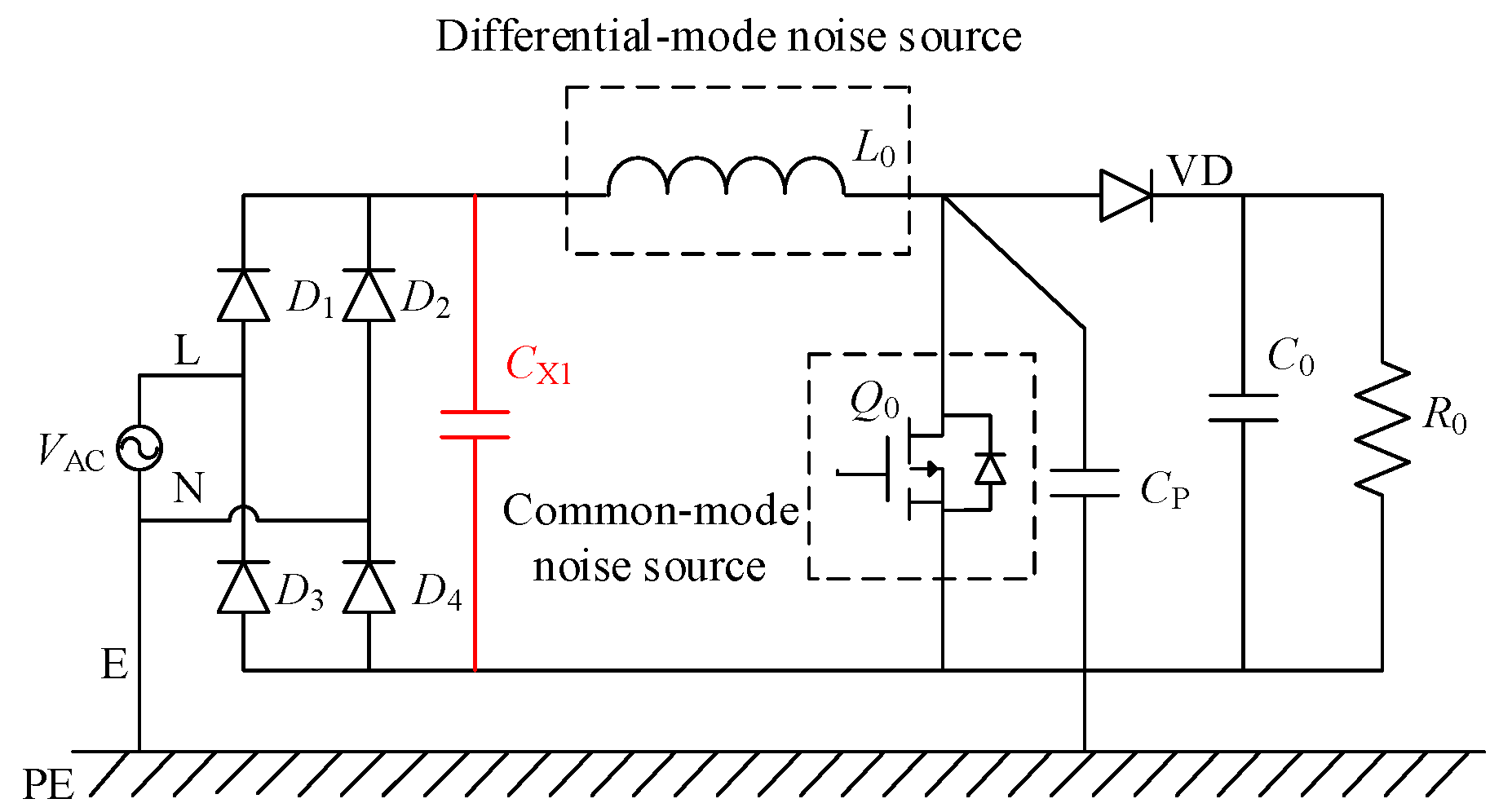
The drain source voltage (
VDS) of the power devices of the boost PFC converter can be considered as the noise voltage source of the CM and DM interferences. It is generally considered that the DM current is mainly caused by the ripple current of the inductor, and the CM current flows mainly from the drain electrode of the switch tube and the parasitic capacitor of the protector, as shown in
Figure 1.
When the current of the inductor L0 is discontinuous, the junction capacitance of inductor L0, the switching device, and the rectifier bridge D1–D4 will induce resonance. The input voltage, after being rectified, will produce voltage spikes that will not only damage the rectifier bridge and switching devices, but also cause common-mode interference. Therefore, the DM capacitor CX1 is usually added behind the rectifier bridge to suppress the voltage spike. At this point, since the capacitance value of differential-mode capacitor CX1 is larger than the junction capacitance value of the rectifier diode and the switch tube, the voltage of capacitor CX1 remains substantially constant when the inductor current is discontinuous. When the rectifier bridge is on, the DM capacitor provides a low-impedance path for the L and N lines, which suppresses the differential-mode interference. If without capacitor CX1, due to impedance imbalance in the circuit, some of the DM current in the boost PFC converter is generated by the CM current.
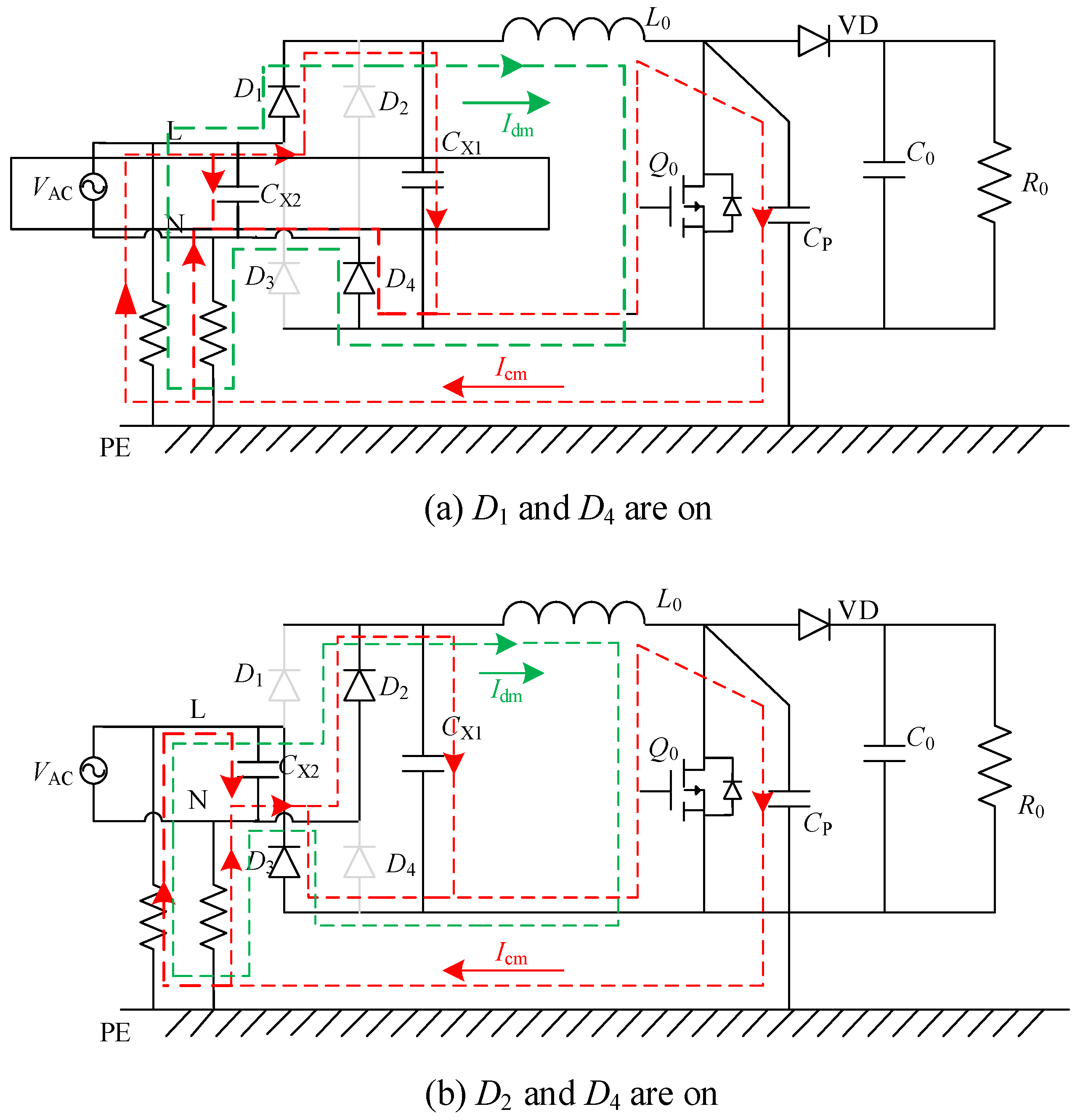
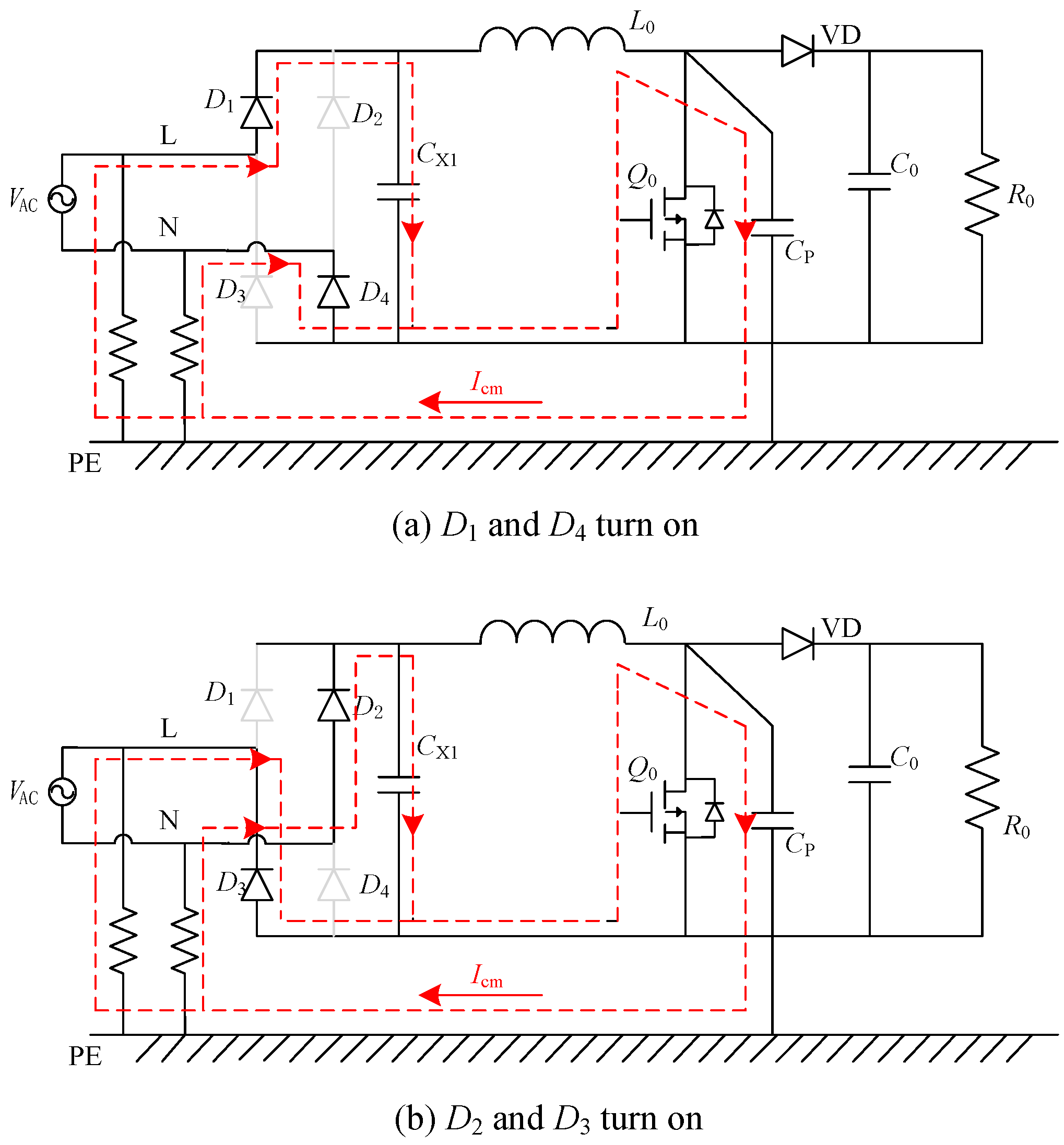
When the rectifier bridge is on, due to the DM capacitance
CX1, the CM current from the chassis almost meets the equivalent impedance. At this time, the CM noise almost equally flows into the L and N lines, where we avoid the CM interference transformation position difference caused by the line impedance unbalance. As shown in
Figure 2, the diodes in grey do not conduct. When the input voltage is positive,
D1 and
D4 conduct; however, the noise reversely flows through diode
D4 because the alternating current (AC) power grid voltage makes the diode conduct. In the negative half-cycle,
D2 and
D3 will conduct, and a similar analysis can be performed. The addition of
CX1 will result in harmonics of the input current and needs to ensure that the frequency is higher than 150 kHz. A
CX1 capacity resistance that is much less than 50 Ω can effectively suppress the mixed interference (the DM interference in part from the CM interference).
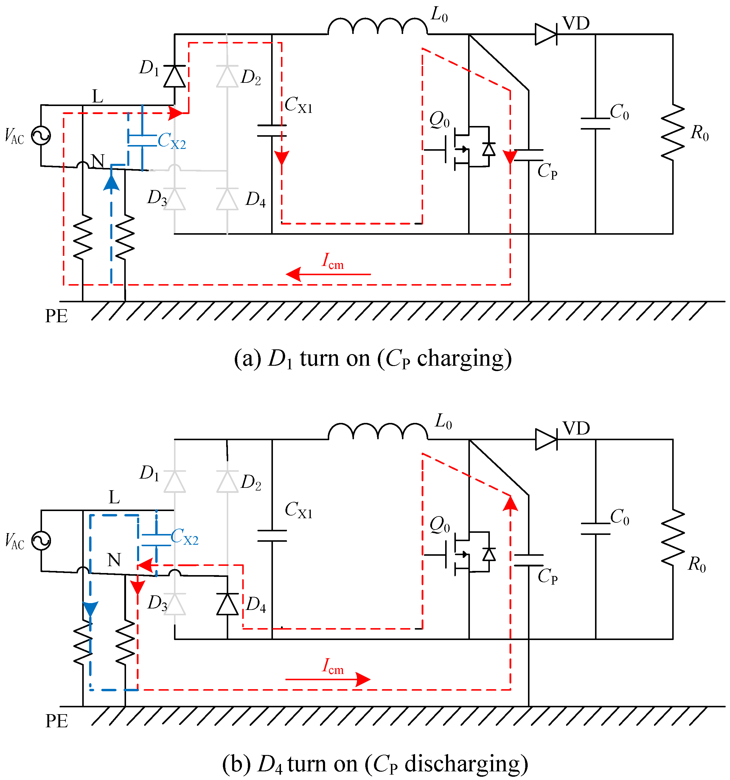
As shown in
Figure 3, the rectifier bridge is off and the CM current passes the test resistor on the L line and
D1, which produces the interference voltage. Obviously, when the CM current does not flow through the L-line and N-line resistors, the DM voltage is generated. In order to inhibit the problem caused by the impedance imbalance, a DM capacitor can be added.
3. Boost PFC CM and DM Equivalent Circuits
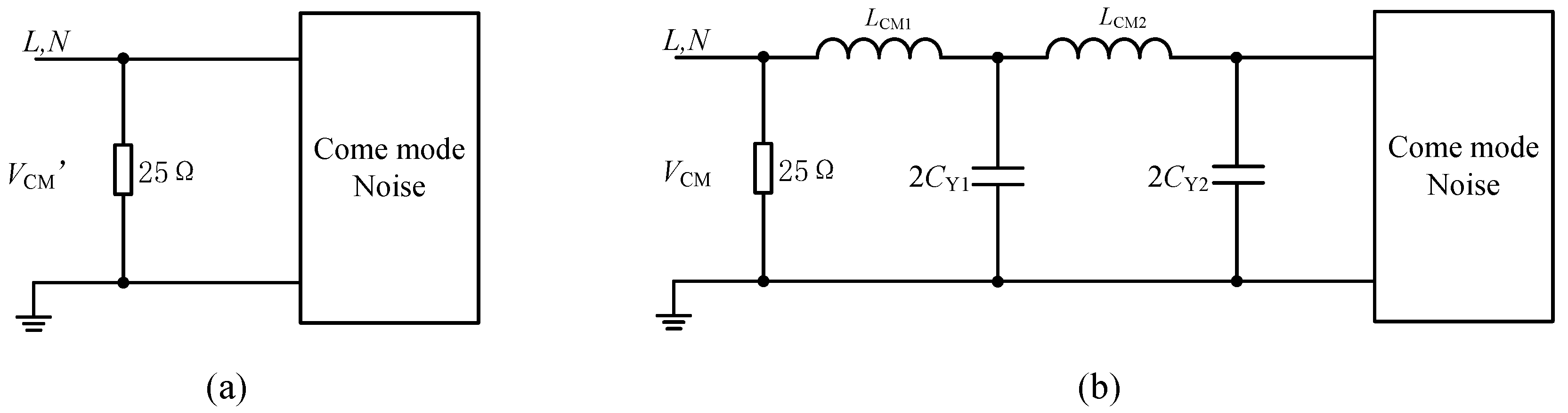
In
Figure 4, the CM and DM interference paths of the boost PFC converter are given, where the capacitors
CX1 and
CX2 are added according to the above discussion. The green dotted line represents the DM interference path, and the red dashed line represents the CM interference path.
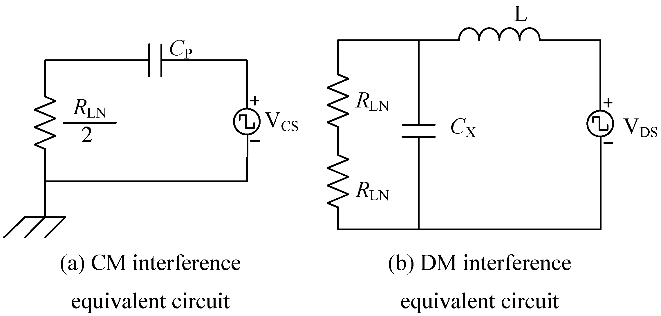
Figure 5 shows the CM and DM equivalent circuit of the boost PFC converter. According to
Figure 4, the filter capacitors
CX1 and
CX2 are parallel. Make
CX =
CX1 +
CX2. In the CM interference branch,
CX is connected in series with the test resistor
RLN on the branch. When the impedance of
CX is smaller than the test resistance
RLN, it can be considered that the filter capacitor
CX is short-circuited, and the test resistance of the L and N lines is equivalent to the parallel connection. Therefore, the test resistance on the CM interference equivalent circuit is
RLN/2, and its CM interference voltage is
VCM. The CM interference equivalent circuit is shown in
Figure 5a. The transmission gain |
TGCM(
f)| of the CM voltage is derived as below.
Due to the parasitic capacitance
CP in the circuit, generally, π
fCPRLN << 1, and the amplitude of the CM interference voltage is derived as below.
Obviously, with the increase of frequency f, the CM interference voltage VCM will increase at a slope of 20 dB/dec. The parasitic capacitance has an obvious influence on CM interference.
Meanwhile, the decrease of voltage VDS will reduce the CM interference.
In the DM interference branch, the DM current flows through the test resistor
RLN of the L and N lines in sequence. Therefore, the test resistance on the DM interference equivalent circuit is 2
RLN, and the DM interference voltage is
VDM. The DM interference equivalent circuit is shown in
Figure 5b. The transmission gain |
TGDM(
f)| of the CM voltage is derived as below.
Usually, when the frequency
f is higher than 150 kHz, 4π
2f 2LCX >> 1 and 4π
2f 2LCXRLN >> π
fL. The amplitude of the DM interference voltage is derived as below.
Obviously, with the increase of frequency f, the DM interference voltage VDM will decline at a slope of −40 dB/dec. Meanwhile, it can be seen from the formula that, in the boost PFC converter, increasing the boost inductor can obviously reduce the DM interference, and decreasing the rate of the up or down of switching devices can reduce the DM interference.
From the above analysis, for the DM and CM interferences, the noise source is the switching device. The DM interference will be converted into CM interference. The parasitic parameters of the boost PFC converter have an impact on the DM and CM interferences. However, the influence is different. The boost inductance mainly affects the DM interference, and the parasitic capacitance between the switching device and the radiator shell mainly affects the CM interference.
4. Model of the CM Inductor and EMI Filter Design
4.1. The High-Frequency Model of CM Inductor
Since the common-mode inductor can achieve a very large inductance value in a very small magnetic core, it is widely used in EMI filters, as it can restrain EMI’s common-mode noise interference very well. In the EMI conduction frequency range, the CM inductor will be affected by the leakage inductance and various parasitic parameters when working at high frequencies, such that its characteristics will change nonlinearly with the frequency. In order to improve the design of EMI filters and to accurately select a common-mode inductor, it is necessary to establish a suitable common-mode inductor high-frequency model in the EMI interference frequency range.
The CM model is more complex, and because of the nonlinearity of the magnetic element, the parameters of the common-mode equivalent model vary with the frequency [
19,
20,
21]. Based on these reasons, a more complex model was used to characterize the high-frequency modeling of CM inductors. The improved model, shown in
Figure 6, was based on the traditional Foster model [
22]. The first level mainly consisted of the core characteristics (influence of iron core, layer number, and turn number), the second level determined the position and amplitude of the second resonant peak, and the third level determined the phase frequency characteristics before and after the second resonance peak, in which stray capacitance
C1 is mainly related to the lead length of the common-mode inductor. The
n-order Foster model can be expressed by
n-harmonic peaks.
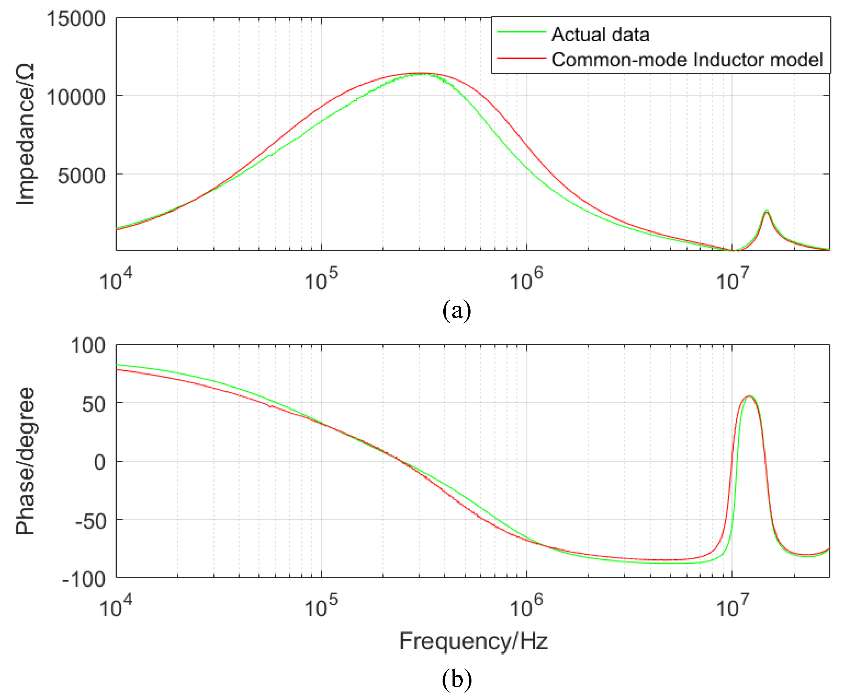
In order to verify the feasibility of the model, an impedance analyzer was used to test the CM inductance sample, and the scanning frequency range was 150 kHz to 30 MHz.
Figure 7 shows the comparison results, fitted using MATLAB.
According to the simulation results in
Figure 7, the high-frequency model of the CM inductor (see
Figure 6) in this paper had a better fitting effect both in impedance (see
Figure 7a) and in phase (see
Figure 7b). Thus, the model circuit shown in
Figure 6 can reflect the change of the CM impedance in the frequency range of 10 kHz to 30 MHz. This improved model is suitable for all kinds of power converters with EMI filters, for example, PFC boost converters, bridgeless converters, and so on.
4.2. EMI Filter Design
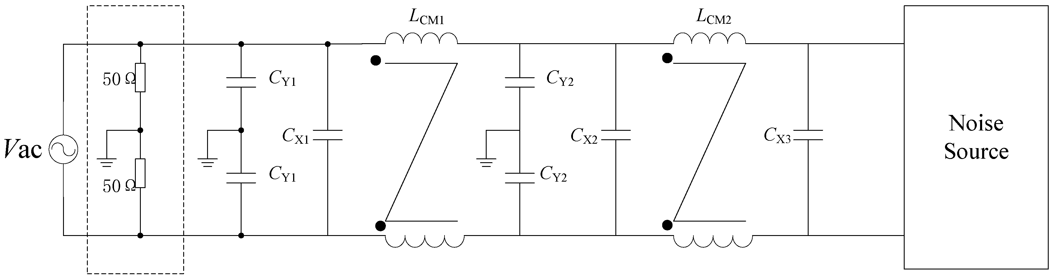
The EMI filter’s attenuation of conducted EMI can be expressed as the voltage insertion gain. The voltage insertion gain is defined as the ratio of the interference voltage measured before and after adding the EMI filter. Similarly, CM and DM equivalent circuits of the EMI filter need to be established, and then the CM and DM attenuation effects of the filter are considered, respectively. The filtering effect of EMI filters is not only related to its own parameters, but is also closely related to interference source impedance. Therefore, in order to design EMI filters efficiently, it is necessary to choose an appropriate filter topology according to different impedance characteristics. In medium and high power of the converters, due to strong common-mode interference, two-stage EMI filters are usually used to suppress interference. In general, the leakage inductance of a CM inductor is used as a DM inductor when designing an EMI filter.
Figure 8 shows the two-stage EMI filter topology. In
Figure 8,
CY1 and
CY2 are CM capacitors and their values are equal,
CX1–
CX3 are DM capacitors, and
LCM1 and
LCM2 are CM inductors.
The attenuation of an EMI filter can be represented by the voltage insertion gain. The common-mode equivalent circuits are shown in
Figure 9. The differential-mode equivalent circuits are shown in
Figure 10.
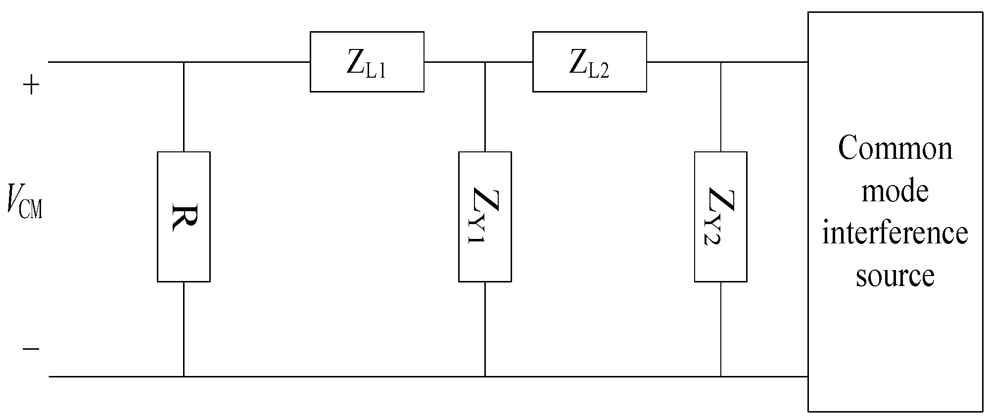
The attenuation can be exemplified by the common-mode equivalent circuit. The CM interference voltage is
V’CM when the filter is not added, and the CM interference voltage is
VCM when the filter is added. Therefore, the CM insertion gain is derived as below.
Figure 11 shows a simplified common-mode equivalent model. According to Equations (8)–(11), the insertion loss of the common mode can be calculated.
According to the previous analysis of the boost PFC circuit and the high-frequency modeling of the common-mode inductor, the high-frequency attenuation performance of the EMI filter can be evaluated more accurately. Meanwhile, it will better suppress the interference of the boost PFC circuit, which helps the reliability of power converters.
5. Experimental Results
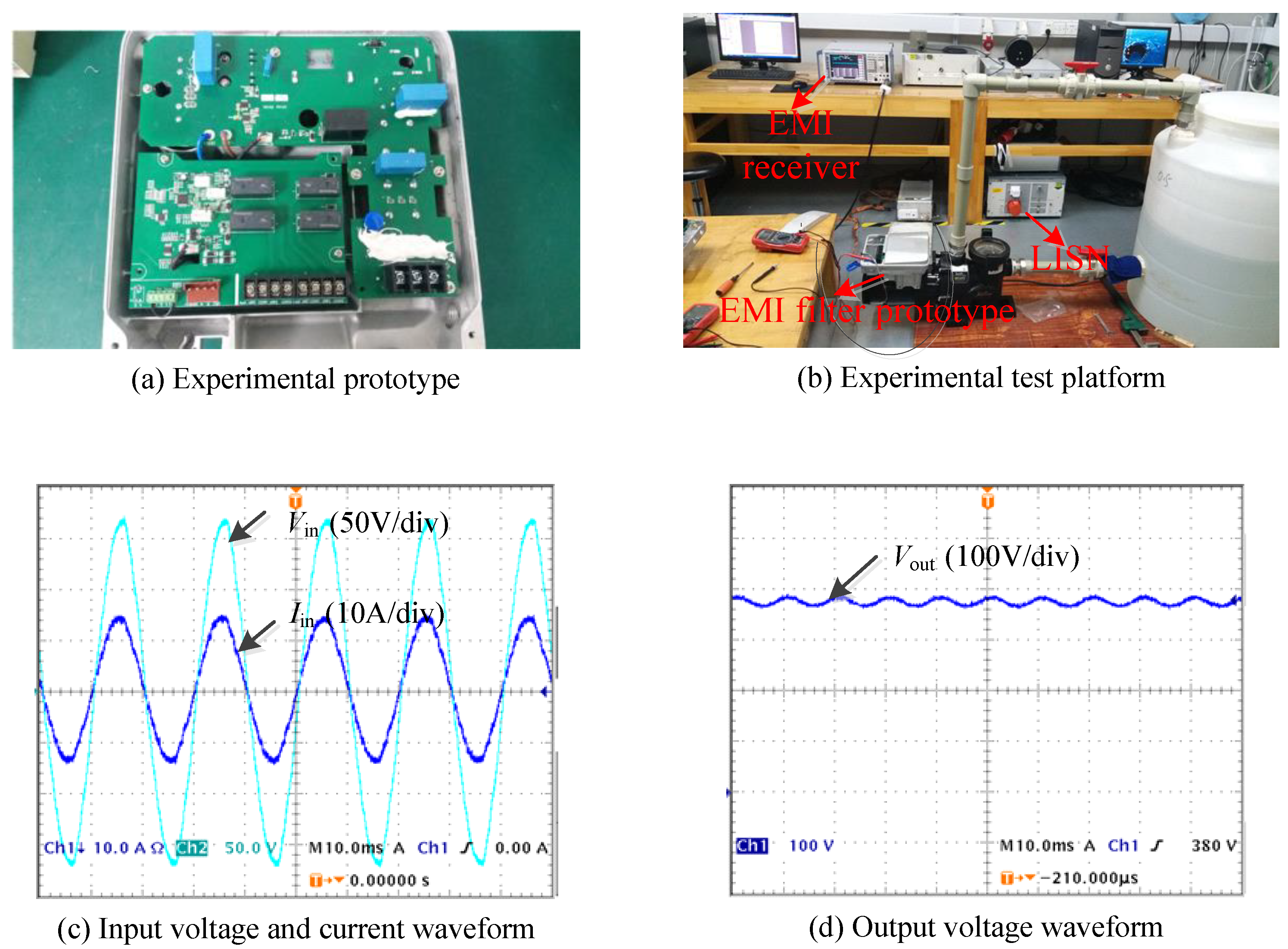
Based on the above analysis, the EMI filter was designed, and the boost PFC converter was optimized. The experimental platform of a 2.4-kW boost PFC motor was built, and the experimental prototype is shown in
Figure 12a.
Figure 12b is the experimental EMI test platform.
Figure 12c shows the input voltage and input current waveforms of the boost PFC converter system.
Figure 12d shows the output voltage waveforms.
Figure 13 shows the EMI conduction test results of the experimental prototype. Clearly, as shown in
Figure 13, the 2.4-kW boost PFC test platform could successfully pass the EMI test. The power factor (PF) of the prototype was very high, and the system could run stably for a long time, thus ensuring the security, reliability, and stability of the system.
6. Conclusions
A boost PFC converter can be used to analyze and suppress the EMI issue of power converters. Here, CM and DM interferences of the boost PFC converter were analyzed and discussed in detail. To alleviate the EMI challenges in the reliability of the entire converter system, a common-mode inductor was designed accordingly and modeled. Using MATLAB simulations, it was found that the improved model, based on the traditional Foster model, could better represent the impedance/frequency characteristics of the common-mode inductor. In addition, the design of the EMI filter could better suppress the CM and DM interferences of the boost PFC converter. EMI-conducted interference could be suppressed using this method. Thus, the reliability of the boost PFC converter was improved. Finally, both simulation results and experimental tests validated the analysis and results.

