Article

Optimized Digital Controllers for Switching-Mode DC-DC Step-Down Converter

1
Electrical Engineering Department, The University of Lahore, Lahore 54000, Pakistan
2
Electrical and Computer Engineering Department, Dalhousie University, Halifax, NS B3H 4R2, Canada
3
Electrical Engineering Department, Riphah International University, Faisalabad 38000, Pakistan
4
Automatics and Applied Software Department, “Aurel Vlaicu” University of Arad, Arad 310130, Romania
*
Author to whom correspondence should be addressed.
Electronics 2018, 7(12), 412; https://doi.org/10.3390/electronics7120412
Submission received: 23 October 2018 / Revised: 5 December 2018 / Accepted: 6 December 2018 / Published: 8 December 2018
(This article belongs to the Section Power Electronics)

Abstract

:
In this paper, a nonlinear least squares optimization method is employed to optimize the performance of pole-zero-cancellation (PZC)-based digital controllers applied to a switching converter. An extensively used step-down converter operating at 1000 kHz is considered as a plant. In the PZC technique, the adverse effect of the (unwanted) poles of the buck converter power stage is diminished by the complex or real zeros of the compensator. Various combinations of the placement of the compensator zeros and poles can be considered. The compensator zeros and poles are nominally/roughly placed while attempting to cancel the converter poles. Although PZC techniques exhibit satisfactory performance to some extent, there is still room for improvement of the controller performance by readjusting its poles and zeros. The (nominal) digital controller coefficients thus obtained through PZC techniques are retuned intelligently through a nonlinear least squares (NLS) method using the Levenberg-Marquardt (LM) algorithm to ameliorate the static and dynamic performance while minimizing the sum of squares of the error in a quicker way. Effects of nonlinear components such as delay, ADC/DAC quantization error, and so forth contained in the digital control loop on performance and loop stability are also investigated. In order to validate the effectiveness of the optimized PZC techniques and show their supremacy over the traditional PZC techniques and the ones optimized by genetic algorithms (GAs), simulation results based on a MATLAB/Simulink environment are provided. For experimental validation, rapid hardware-in-the-loop (HiL) implementation of the compensated buck converter system is also performed.

1. Introduction

Modern-day digital devices such as cellular phones, camcorders, calculators, digital cameras, portable electronic devices, microprocessors, DSP core, handheld computers and PDAs, MP3 personal players, and so on utilize switch-mode power supplies (SMPSs). The devices need to have regulated output voltages irrespective of the perturbation in the input voltage or load current. For this purpose, traditionally, analog controllers have been applied to SMPSs to ensure regulated voltages for the digital devices. Analog controllers, however, show limitations in the form of poor design portability, large size, low reliability, and low flexibility. Digital controllers, on the other hand, offer advantages in the form of high flexibility and programmability, competency to implement complex control strategies, no need to alter hardware upon changing algorithms, high performance/cost ratio, and excellent dynamic performance, among others [1]. Consequently, SMPS designers are more interested in developing efficient and optimized digital controllers as compared to the predominately used analog controllers. In this paper, well-recognized PZC techniques-based optimized digital controllers are designed for buck converters to display much-improved performance. One of the optimization techniques, named the nonlinear least squares technique, is employed to optimize the performance of PZC-based digital controllers.
As far as the literature review is concerned, in [2], a pole-zero-cancellation technique-based digital controller for a buck converter was suggested by Abe et al. to improve the performance characteristics. The effect of the resonance peak and ESR-zero is nullified by completely cancelling the poles and the zero of the buck converter with the help of the complex zeros and the pole of the compensator, respectively. An additional pole representing a simple low-pass filter is introduced to gain control of the characteristics of the composite buck converter system. A two-pole two-zero analog controller is mapped into the digital controller using bilinear transformation. In [3], the same authors (Abe et al.) applied successfully the two-pole two-zero analog compensator to the buck and boost converters to ensure superior performance, yet without cancelling the RHP-zero in the case of the boost converter. The effect of change in the capacitance of the output capacitor in a PZC-based digitally controlled buck converter on the stability margin, and thus the performance, was investigated in [4]. Reference [5] also suggested the application of a three-pole two-zero (analog) compensator with complex as well as real zeros to a switching converter exhibiting nonminimum phase characteristics. Such a converter possesses RHP-zero in its transfer function, which limits the bandwidth, thus causing the response to be slow and sluggish. Reference [6] suggested a slightly different approach for designing a PZC-based digital controller for the step-down converter. Rather than using the real or complex zeros by the compensator close to the resonant frequency of the converter’s power stage, the compensator zeros are selected on the basis of the quality factor and output impedance of the plant. The effect of the quality factor on compensator design is also investigated efficiently. In [7], the task of providing feedback compensation to the relatively complicated switching converters (as they involve RHP-zero), namely boost and flyback working in continuous conduction mode, was efficiently performed through various combinations of PZC-based controllers. The PZC-based digital controllers mentioned in the aforementioned references show somewhat satisfactory performance. Their performance may even be improved by retuning their coefficients through some optimization techniques.
Many researchers successfully applied advanced numerically based or metaheuristic optimization techniques to tune the compensator parameters to ameliorate performance. Reference [8] suggested the tuning of the parameters of the digital controller designed on the basis of a Chebyshev polynomial approach for the fifth-order boost converter through a genetic algorithm (GA). The problem with the GA is that it has to employ its three operators, namely selection, crossover, and mutation, at each iteration, thus resulting in slower responses. In addition, it shows enhanced sensitivity to the initial population and does not use gradients. In [9], although metaheuristic techniques such as particle swarm optimization (PSO) and the gravitational search algorithm (GSA) were successfully employed for the fine-tuning of parameters of Type II and Type III compensators applied to a step-up converter, but they may converge prematurely. Mercader et al. in [10] tried to overcome the problem of convergence to the local minimum of convex optimization and proposed a convex-concave procedure (CCP) for the fine-tuning of PID controller coefficients that controlled the loop shape efficiently to ensure better dynamic performance. On the other hand, the NLS method capitalizes on the structure of the Hessian, which can be attained through the computation of Jacobian (first-order derivatives only) and minimizes the errors (residuals) quickly, and thus ensures better set-point tracking.
In addition, many instances in the literature have been reported where the nonlinear least squares (NLS) method has been successfully employed to optimize the performance of various types of compensators used for various applications. In [11], optimization of the discrete root locus-based discrete-time controller applied to a buck converter was accomplished through the NLS method. In [12], tuning of the PID-based track-keeping controllers of a remotely controlled autonomous in-scale fast-ferry model was carried out through the NLS method and a genetic algorithm (GA), where the former showed superiority over the latter one while doing sea trials. Reference [13] suggested the use of the NLS method for the optimization of offline pulse patterns for arbitrary modulation indices and arbitrary numbers of modules per branch, while minimizing the harmonic content of the load current (specifically measured in the total demand distortion (TDD)), instead of using selective harmonic elimination, in the case of the indirect modular multilevel converter (MMC). In [14], a Levenberg-Marquardt (LM) and quasi-Newton (QN)-based NLS hybrid method was used efficiently to improve the performance of the designed linear-phase quadrature mirror filter (QFM) bank in the form of mean squares error in passband and stopband regions, as well as peak reconstruction error (PRE) and error in the transition band at quadrature frequency. This was accomplished by optimizing the quadratic measure of the ideal characteristics of the prototype filter and filter bank at quadrature frequency. In [15], a predictive current controller with an extended-state observer (ESO), suggested for the grid integration of wind energy systems, utilized the NLS method to minimize a cost function, defined as a sum of the squared values of d-axis and q-axis current errors, while computing the optimal converter switching time. In [16], calibration of the roadside camera employed in traffic surveillance systems was accomplished on the basis of the least squares optimization method, which involved camera-intrinsic parameters and rotation angles. In [17], for anticipating the epileptic seizure via EEG signals in epileptic individuals suffering from unexpected and momentary electrical deterioration in the brain, fitting of the EEG signals filtered through singular spectrum analysis into the exponential curve was carried out using the NLS method. Statistical examination of the features extracted from exponential curves assists in diagnosis. In [18], nonlinear rational systems were identified using an NLS-based, globally consistent two-step estimator. In [19], a high face recognition rate was achieved by performing NLS computations, while taking into account the ‘holistic’ and ‘detailed’ features of the face.
Although enormous numbers of examples of the application of the NLS method to control plants of various types are found in the literature, to the best knowledge of the authors, very limited instances are found in the literature where pole-zero-cancellation-based digital controllers have been optimized through the NLS method. In this paper, PZC-based optimized digital controllers are, thus, suggested for the buck converter to achieve much-improved performance.
The paper is formulated in the following way. Section 2 describes the dynamics of the buck converter, which is considered to be the plant in the paper. Three types of pole-zero-cancellation (with complex and real zeros)-based digital controllers are designed in Section 3. The digital controller design techniques are essentially of the types digital redesign or emulation. The NLS method involving the LM algorithm to optimize the digital controllers is detailed in Section 4. Nonlinearities involved in the digital control loop are modelled in Section 5. Section 6 involves the redesigning and reoptimizing of the digital controllers when the nonlinear effects in the digital control loop are considered. Section 7 is dedicated to additional simulation results. HiL implementation is described in Section 8. Concluding remarks are given in Section 9.

2. Buck Converter Modelling

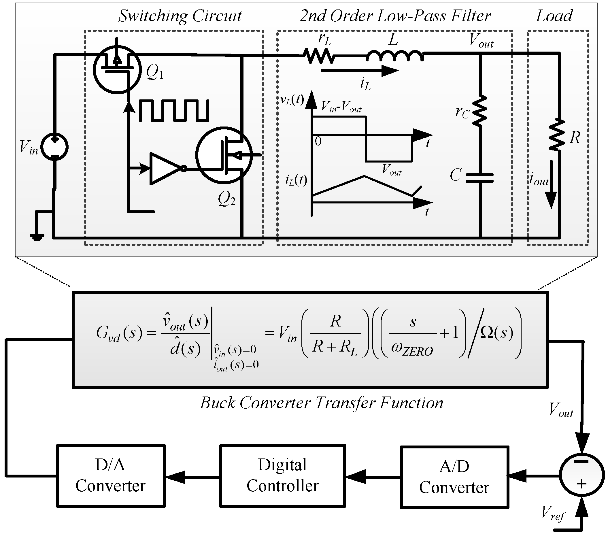
For the sake of reducing higher unregulated DC input voltage, Vin, to lower regulated DC output voltage, Vout, a realistic buck converter circuit (see Figure 1) is used, as it takes into consideration the parasitic resistances, i.e., capacitor equivalent series resistance (ESR) and inductor direct current resistance (DCR), denoted explicitly by rC and rL, respectively. Owing to capacitor ESR, a zero is introduced into the buck converter transfer function [20]. The component values to be considered for the converter throughout the paper are the following: Vin = 3.6 V, Vout = 2.0 V, L = 4.7 µH, C = 4.7 µF, rL = 505 mΩ, rC = 5 mΩ, fs = 1000 kHz, and Ts = 1/fs = 1 µs. The block diagram of the closed-loop (digital) control system containing the buck converter power stage, ADC and DAC converters, and the digital controller is shown in Figure 1.
The buck converter’s dynamics (transfer function) imperative for the controller design can be derived through its small-signal AC-equivalent circuit model (see Figure 2), where the nonlinear power switches Q1 and Q2 are replaced by their equivalent linear small-signal models [21]. By applying the averaging and linearization technique adopted in [22] to the small-signal model, the small-signal transfer functions, such as duty cycle-to-output voltage G v d ( s ) , input voltage-to-output voltage G v g ( s ) , and load current-to-output voltage (loaded power converter output impedance Z o ( s ) ), can be computed and are described by Equations (1)–(3), respectively [22,23].
G v d ( s ) = v ^ o u t ( s ) d ^ ( s ) | v ^ i n ( s ) = 0 i ^ o u t ( s ) = 0 = V i n ( R R + r L ) ( s ω Z E R O + 1 Ω ( s ) )
G v g ( s ) = v ^ o u t ( s ) v ^ i n ( s ) | d ^ ( s ) = 0 i ^ o u t ( s ) = 0 = D ( R R + r L ) ( s ω Z E R O + 1 Ω ( s ) )
Z o ( s ) = v ^ o u t ( s ) i ^ o u t ( s ) | d ^ ( s ) = 0 v ^ i n ( s ) = 0 = r L ( R R + r L ) ( ( s ω L + 1 ) ( s ω Z E R O + 1 ) Ω ( s ) )
where
Ω ( s ) = ( s 2 ω 0 2 + s Q ω 0 + 1 )
ω 0 = 1 L C R + r C R + r L 1 L C , if   { r C < < R r L < < R
Q = Q L O S S Q L O A D = 1 2 ζ = 1 ω 0 ( L R + r L + R r L C R + r L + r C C ) 1 ω 0 ( L R + r L C + r C C ) , if { r C < < R r L < < R
ω Z E R O = 1 r C C
and
ω L = r L / L
Here ω 0 , ω Z E R O , and Q represent the filter resonance frequency, capacitor zero frequency, and the quality factor of the filter, respectively.
Among the transfer functions, the one described in Equation (1), i.e., duty cycle-to-output voltage, is controlled through the controller for output voltage regulation. To achieve the closed-loop characteristics, and thus required performance, a controller is applied to it as it behaves as a plant. The G v d ( s ) contains a complex conjugate pair whose effect can be nullified by the complex or real zeros of the compensator.
In order to design the digital controller, the continuous-time converter transfer function G v d ( s ) is discretized using zero-order-hold (ZOH) with a sampling period T s , as follows:
G p ( z ) = Z { 1 e s T s s G v d ( s ) } = ( 1 z 1 ) Z { G v d ( s ) s }
For the component values mentioned above, the transfer function in the analog and digital form of the buck converter with a short description is presented in Table 1.

3. PZC-Based Digital Controllers

The buck converter power stage contains two complex conjugate poles occurring at the LC filter’s resonant frequency, which results in phase reduction, thus making the system unstable. In order to meet the required specifications, such as bandwidth, steady-state accuracy (ensured through static-error constant/DC gain of the system), robust relative stability, reduced sensitivity to parameter changes, superior transient response, and so on, appropriate gain and phase margins at a specific 0-dB crossover frequency and loop gain should be ensured. This can be accomplished by placing the compensation zeros, real or complex, near the LC filter’s resonant frequency. Such a pole-zero-cancellation (PZC) technique in analog form is employed in the paper for designing the digital controllers (emulation technique), which are then optimized using the NLS method. Three types of PZC techniques, designed for a 100 kHz, 0-dB crossover frequency (10 times below the switching frequency, to satisfy the Nyquist criterion), unless otherwise stated, distinguished on the basis of placement of compensator’s zeros and poles, are designed to ensure better static and transient responses. All the cases involve the same method of computing the compensator gain. For the design of PZC techniques, the same procedure is adopted, which is outlined in the flow chart shown in Figure 3.

3.1. A Three-Pole Two-Zero Compensator—Case 1

3.1.1. Using Complex Zeros

In this type of PZC technique, the effect of a pair of complex poles of the converter is nullified by placing the two complex zeros of the compensator at the LC resonant frequency (ω0). This actually adds to the phase to boost the phase margin. One of the compensator poles is placed at the ESR zero (ωZERO) to keep the gain of the open-loop transfer function at a slope of −1. For the rejection of high-frequency noises, the second high-frequency pole is moved from approximately 0.2 to 0.7 of the switching frequency. This additionally incorporated high-frequency pole not only makes the compensator less sensitive to high-frequency noise phenomena, but also assists in smoothing the quantization error in the compensator output. To achieve zero steady-state error, an integrator (a pole at origin) is also introduced.
With the mentioned placement of the compensator poles and zeros, the compensator transfer function takes the form
G c ( s ) = K c ( s 2 ω z 2 + s Q C ω z + 1 ) s ( s k ω s + 1 ) ( s ω Z E R O + 1 )
where parameter k , ranging from 0.2 to 0.7, controls the location of the high-frequency pole; ω z = ω 0 designates the compensator complex zero frequencies, numerically equivalent to the plant poles’ resonance frequencies; the dimensionless Q-factor, Q C , of the compensator is selected close to the power stage, Q ; and the DC gain, K c , of the compensator is adjusted to meet the required 0-dB crossover frequency (100 kHz) denoted by ω x . Then, s x = j ω x = j 2 π f x .
Assuming the condition that the compensated system’s gain plot crosses 0-dB at a −1 slope, i.e., G p ( s ) | s = s x G c ( s ) | s = s x = 1 , K c is then calculated by
K c = s ( s k ω s + 1 ) ( s ω Z E R O + 1 ) ( s 2 ω z 2 + s Q C ω z + 1 ) | s = s x 1 G p ( s ) | s = s x
With the placement of poles and zeros and calculation of the DC gain, the analog controller transfer function is given, numerically, by:
G c ( s ) = 4.309 × 10 6 s 2 + 0.6041 s + 1.951 × 10 5 3.74 × 10 15 s 3 + 1.827 × 10 7 s 2 + s
The continuous-time compensator can be mapped into its discrete-time counterpart using one of the transformation techniques, such as ‘Tustin’ (in our case), expressed mathematically by s = 2 T s ( 1 z 1 1 + z 1 ) , with the sampling time equivalent Ts = 1 µs. The corresponding discrete-time compensator is given by:
G c ( z ) = 6.753 z 3 5.595 z 2 6.47 z + 5.877 z 3 + 0.4273 z 2 0.9566 z 0.4707 = 6.753 5.595 z 1 6.47 z 2 + 5.877 z 3 1 + 0.4273 z 1 0.9566 z 2 0.4707 z 3
With the help of an inverse z-transform, the compensator discrete-time transfer function can be translated into the difference equation given by
u [ n ] = 0.4273 u [ n 1 ] + 0.9566 u [ n 2 ] + 0.4707 u [ n 3 ] + 6.753 e [ n ] 5.595 e [ n 1 ] 6.47 e [ n 2 ] + 5.877 e [ n 3 ]
where e[n], e[n − 1], e[n − 2], and e[n − 3] designate the current, one sample period, two sample period, and three sample period delayed values of the error signals, respectively, whereas u[n], u[n − 1], u[n − 2], and u[n − 3] represent the present, one sample period, two sample period, and three sample period delayed values of the duty ratio, respectively.

3.1.2. Using Real Zeros

A compensator with three poles and two real zeros can also be realized and is expressed by
G c ( s ) = K c ( s ω z 1 + 1 ) ( s ω z 1 + 1 ) s ( s k . ω s + 1 ) ( s ω Z E R O + 1 )
Usually, the real zeros ω z 1 and ω z 2 are placed close to the resonant frequency, ω 0 . Their positions can be controlled using the relationships: ω z 1 = m 1 ω 0 and ω z 2 = m 2 ω 0 , where the coefficients m 1 and m 2 describe the deviation of the zeros from ω 0 . Here, in our case, it is observed that placement of one of the zeros at ω 0 , i.e., m 1 = 1 , and the other slightly below ω 0 , i.e., m 2 = 0.8 , ensures the increase in phase margin, thus the better performance. The compensator’s three poles are placed in the same way as described in the complex zeros case.
With such an arrangement of poles and real zeros, the analog controller, numerically, takes the form
G c ( s ) = 3.597 × 10 6 s 2 + 1.378 s + 1.303 × 10 5 3.74 × 10 15 s 3 + 1.827 × 10 7 s 2 + s
The digital controller obtained from the analog controller using the bilinear mapping technique is then described by
G c ( z ) = 6.257 z 3 4.072 z 2 6.069 z + 4.261 z 3 + 0.4273 z 2 0.9566 z 0.4707
When comparing the analog compensators with real and complex zeros and the digital compensators, the following corollaries can be deduced.
  • It is revealed from the inspection of the Bode plots (see Figure 4) of the open-loop compensated buck converter system that the compensator using the complex zeros at the resonance frequency achieves a phase margin of 84.3°, as compared to the one with real zeros, which attains a phase margin of 64.6°. Both the compensators are designed for 100-kHz bandwidth (0-dB crossover frequency). This suggests that complex-zero compensation offers larger stability margins and reduced amplitude of the resonance peak, in comparison to that of the real-zero compensation. Consequently, complex-zero compensation displays excellent static properties.
  • Unlike the excellent static properties, complex-zero compensation shows poor dynamic properties. In order to check the dynamicity, the load is changed from 4.5 Ω to 9 Ω and then from 9 Ω to 4.5 Ω. Although the output voltage settles to its steady-state value of 2 V for both compensators, the compensator with complex zeros shows more recovery time and spike voltage peak at the load transient as compared to that of the one with real zeros. This is due to the fact that a change in load displaces the converter poles from their original positions. Thus, the predetermined compensator zeros are not able to perfectly annul the effects of the converter’s complex poles. If the compensator zeros are made adaptive according to the perturbation in the load current, then the complete cancellation effect can be ensured. MATLAB/Simulink-based simulation results shown in Figure 5 highlight this fact.
Transformation of the continuous-time controller into the discrete-time controller results in frequency distortions. Consequently, the discrete-time controller shows a slightly deviated behavior from its analog counterpart at frequencies close to the Nyquist frequency. The Bode plot of the analog and digital compensators (see Figure 6) pinpoints the phenomenon of frequency distortions.

3.2. A Two-Pole (with One Pole at the Origin) Two-Zero Compensator—Case 2

3.2.1. Using Complex Zeros

Reasonable compensation can also be achieved using two poles (with two complex zeros), rather than using three poles. The poles and the (complex) zeros are placed in the same way as described in case 1. For example, in a two-pole two-zero compensator, a pair of matching complex zeros is placed exactly at the resonance frequency to nullify the effects of a pair of complex conjugate poles introduced by the converter power stage. In order to avoid undesirable ripples in the output voltage introduced by the output capacitor ESR, one of the compensator poles is placed at the ESR zero frequency to compensate for the capacitor ESR zero. For the sake of ensuring high low-frequency gain to achieve low static error and good input rejection, a pole (an integrator) is placed at the origin. Such a two-pole two-zero compensator, in transfer function form, is described by [24] as follows:
G c ( s ) = K c ( s 2 ω z 2 + s Q C ω z + 1 ) s ( s ω Z E R O + 1 )
With K c computed from the condition G p ( s ) | s = s x G c ( s ) | s = s x = 1 , the compensator’s transfer function in the s-domain, numerically, takes the form as follows:
G c ( s ) = 4.288 × 10 6 s 2 + 0.6011 s + 1.941 × 10 5 2.35 × 10 8 s 2 + s
The analog controller is mapped into the digital one with the help of the Tustin mapping technique using a sampling time of 1 µs, as follows:
G c ( z ) = 8.858 z 2 16.2 z + 7.71 z 2 0.08978 z 0.9102

3.2.2. Using Real Zeros

With the real zeros replacing the complex zeros, the transfer function of a two-pole two-zero compensator is then described by
G c ( s ) = K c ( s ω z 1 + 1 ) ( s ω z 2 + 1 ) s ( s ω Z E R O + 1 )
Regarding the placement of the zeros, one of the real zeros is placed at ω 0 , i.e., m 1 = 1 , and the other slightly below ω 0 , i.e., m 2 = 0.8 . This combination ensures the increase in phase margin, thus better response characteristics. With the placement of compensator poles and zeros and the adjustment of gain Kc to achieve the desired crossover frequency, the analog controller reduces to
G c ( s ) = 3.512 × 10 6 s 2 + 1.495 s + 1.59 × 10 5 2.35 × 10 8 s 2 + s
Using the bilinear transformation with 1 µs, the discrete controller, equivalently, is expressed by
G c ( z ) = 8.213 z 2 13.27 z + 5.358 z 2 0.08978 z 0.9102

3.3. A Two-Pole Two-Zero Compensator—Case 3

3.3.1. Using Complex Zeros

Another type of a two-pole two-zero compensator can be achieved by placing a pole at the origin with a low-frequency pole. In such a compensator, the buck converter transfer function is completely cancelled with the complex zeros (occurring at resonance frequency) and a pole (placed at the ESR zero frequency) of the compensator. Thus, the phase shift introduced by an LC filter complex double pole and output capacitor ESR zero is annulled by making the converter characteristics ineffective. Through the remaining part of the compensator (gain and a low-frequency pole), which is essentially a low-pass filter, the composite system’s response is thus controlled. Mathematically, the transfer function of the compensator is given by
G c ( s ) = K c ( s ω p + 1 ) ( s 2 ω z 2 + s Q C ω z + 1 s ω Z E R O + 1 )
With the low-frequency pole placed far below (approximately 103 times) fs, the compensator is described, numerically, by
G c ( s ) = 6.825 × 10 10 s 2 + 9.567 × 10 5 s + 30.9 3.74 × 10 12 s 2 + 1.592 × 10 4 s + 1
Using the Tustin mapping technique, the analog controller is mapped in to the digital controller as follows:
G c ( z ) = 8.831 z 2 16.15 z + 7.686 z 2 0.08352 z 0.9045
For the controllers designed for the 100-kHz crossover frequency, the analog control system offers a phase margin of about 90.6°, whereas the digital control system provides a phase margin of 72.7° (see Figure 7). Frequency distortion due to the mapping from the s-plane to z-plane deteriorates the performance of the digital controller. This requires the retuning of the coefficients of the digital controller.

3.3.2. Using Real Zeros

A two-pole two-zero compensator with one of the poles lying at low frequency and real zeros lying in the vicinity of the resonance frequency is characterized by the transfer function as follows:
G c ( s ) = K c ( s ω z 1 + 1 ) ( s ω z 2 + 1 ) ( s ω p + 1 ) ( s ω Z E R O + 1 )
Numerically, the analog controller is given by
G c ( s ) = 3.512 × 10 6 s 2 + 1.495 s + 1.59 × 10 5 2.35 × 10 8 s 2 + s
The equivalent discrete-time controller using the bilinear transformation is expressed by
G c ( z ) = 8.213 z 2 13.27 z + 5.358 z 2 0.08978 z 0.9102

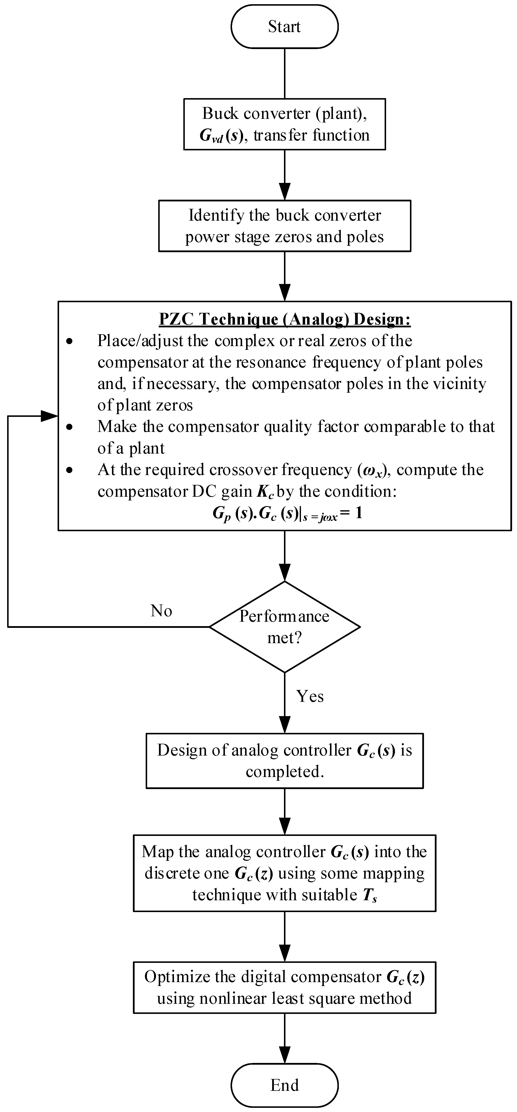
4. NLS Method-Based Optimized Digital Controllers

In the context of optimization, the nonlinear least squares (NLS) method bears a tempting structure that can be exploited with great effectiveness in algorithm design. Regarding the compensated buck converter system, minimization of the voltage error signal essentially constitutes the NLS problem. Specifically, the NLS technique can be employed to retune the discrete-time controller coefficients for fast setpoint tracking. This is accomplished by adjusting the controller coefficients to speedily reduce the error e(t) = VoutVref at all steps of the simulation time. As the minimization of the sum of squares of the error functions is carried out by the algorithm at each step, this constitutes the multiobjective optimization problem.
In the paper, for calculating the sum of error squares, among the different large-scale algorithms [25], such as the trust-region-reflective (TRR), variable projection (VP), and Levenberg–Marquardt (LM) algorithms, LM is employed. Linear algebra is exploited in large-scale algorithms which do not require or store full matrices for its operation. It is a well-established fact that the LM algorithm performs better when bound constraints are not considered in the problem.
The algorithm starts with the initial design vector, x0, indicating the initial design variables in the form of coefficients of the digital controller computed through the pole-zero-cancellation techniques. For the considered cases, no restriction has been imposed on the lower and upper bounds of the design variables.
Mathematically speaking, the NLS method using the LM algorithm involves minimizing the sum of squares of the error signal, i.e.,
min x n f ( x ) = min x n e ( x ) 2 2 = min x n ( e 1 2 ( x ) + e 2 2 ( x ) + + e m 2 ( x ) ) = min x n i = 1 m e i 2 ( x )
subject to the constraints:
{ A e q x = b e q linear   equality A . x b linear   inequality l x u bounds C ( x ) = 0 nonlinear   equality C e q ( x ) 0 nonlinear   inequality
where x = ( x 1 , x 2 , , x n ) n , l ( ( ) ) n , and u ( ( ) ) n . Here, A and A e q , and C and C e q are the matrices of doubles for linear inequalities and equalities, and nonlinear inequalities and equalities, respectively. Similarly, b and b e q are the vectors of doubles for linear inequalities and equalities, respectively, and l and u represent the lower and upper bounds, respectively, on each x component. In our case, since no restriction is imposed on the bounds of design variables for the unconstrained multiobjective optimization problem, all matrices and vectors are empty sets. Here, the function to be minimized, f ( x ) = e ( x ) 2 2 , representing the l2-norm of error, is assumed to be continuously differentiable at point x 0 . It is assumed that m n . As remarked, the vector x represents the number of design/decision variables, which are specifically the coefficients of the digital controllers.
In the compensated control systems, in order to achieve the targeted trajectories realistically, the residual e ( x ) , being a function from n to m , described in Equation (31)
e ( x ) = e i ( x ) = [ e 1 ( x ) e 2 ( x ) e m ( x ) ] = [ v o ( x , t 1 ) v r e f ( t 1 ) v o ( x , t 2 ) v r e f ( t 2 ) v o ( x , t m ) v r e f ( t m ) ]
is made small optimally and converged speedily. Rapidly converged minimum residuals result in better set-point tracking. A unique solution is guaranteed due to the convex nature of the minimizer.
In order to get deep mathematical insight, the algorithm forces the output v o ( x , t ) to track the continuous required trajectory v r e f ( t ) for the decision vector x and scaler t. That is to say,
min x n t 1 t 2 ( v o ( x , t ) v r e f ( t ) ) 2
Discretization of the integral through an appropriate quadrature formula reduces Equation (32) to the least squares problem:
min x n e ( x ) 2 2 = min x n i = 1 m ( v o ( x , t i ) v r e f ( t i ) ) 2
A m-by-n-sized Jacobian matrix J ( x ) of the residual e ( x ) of n variables is computed by
J ( x ) = δ e i ( x ) δ x k ,   1 i m ,   1 k n
On the basis of J ( x ) , the specially structured gradient vector G ( x ) and Hessian matrix H ( x ) of the NLS method are calculated by Equations (35) and (36), respectively.
G ( x ) = e ( x ) 2 2 = i = 1 m e i ( x ) e i ( x ) = 2 ( J ( x ) T e ( x ) )
H ( x ) = 2 e ( x ) 2 2 = 2 ( J ( x ) T J ( x ) + i = 1 m e i ( x ) 2 e i ( x ) ) = 2 ( J ( x ) T J ( x ) + Q ( x ) )
where
Q ( x ) = i = 1 m ( e i ( x ) × H i ( x ) )
The matrix Q ( x ) comes with the property that it tends to approach zero as the residual e ( x ) approaches zero on the occasion the decision variables x k , finally settling to optimal values. In other words, the matrix Q ( x ) gives an indication of how fast the minimization of the error is accomplished.
By amalgamating the salient characteristics of the Gauss–Newton (GN) and steepest descent (SD) algorithms, the LM method computes the search direction on the basis of a solution of the linear set of equations [26], i.e.,
( J ( x k ) T J ( x k ) + λ k I ) d k = J ( x k ) T e ( x k )
More precisely, the LM method modifies the GN search direction by altering J ( x k ) T J ( x k ) with J ( x k ) T J ( x k ) + λ k I . By replacing the identity matrix with the diagonal of the Hessian, Equation (38) can be expressed alternatively as
( J ( x k ) T J ( x k ) + λ k d i a g ( J ( x k ) T J ( x k ) ) ) d k = J ( x k ) T e ( x k )
Or, equivalently, in terms of the least squares problem, Equation (39) takes the form
min d k ( J ( x k ) λ k d i a g ( J ( x k ) T J ( x k ) ) ) ( e ( x k ) 0 ) 2 2
The magnitude and direction of d k is controlled through the scalar λ k , whose initial value λ 0 is set empirically, perhaps, as 100. The LM method therefore uses a search direction that falls within the directions calculated by the GN and SD methods. The LM algorithm, thus, essentially is an aggregation of the SD and GN algorithms. For example, when λ k is zero, the direction d k refers to the direction of the GN method, whereas when λ k tends to infinity, d k assumes the direction of SD, with its magnitude tending to zero. This comes with the observation that the term e ( x k + d k ) < e ( x k ) holds true for some adequately large values of λ k . Through the control of the term λ k , descent can be ensured even when second-order terms, which limit the GN method’s efficiency, are experienced. The algorithm adjusts the value of λ k during each of the step as follows:
λ k + 1 = { λ k 10 , when   the   move   passes λ k × 10 , when   the   move   fails
In a nutshell, the LM algorithm works in the following way:
  • It starts with an initial guess x 0 and iterates for k = 1 , 2 , , n .
  • The Lagrange multiplier λ k is then selected for each step k .
  • Equation (39) or (40) is solved for determining d k .
  • For the next iteration, k + 1 , d k + 1 = d k + Δ d k is calculated.
  • At the end, the solution is checked for convergence.
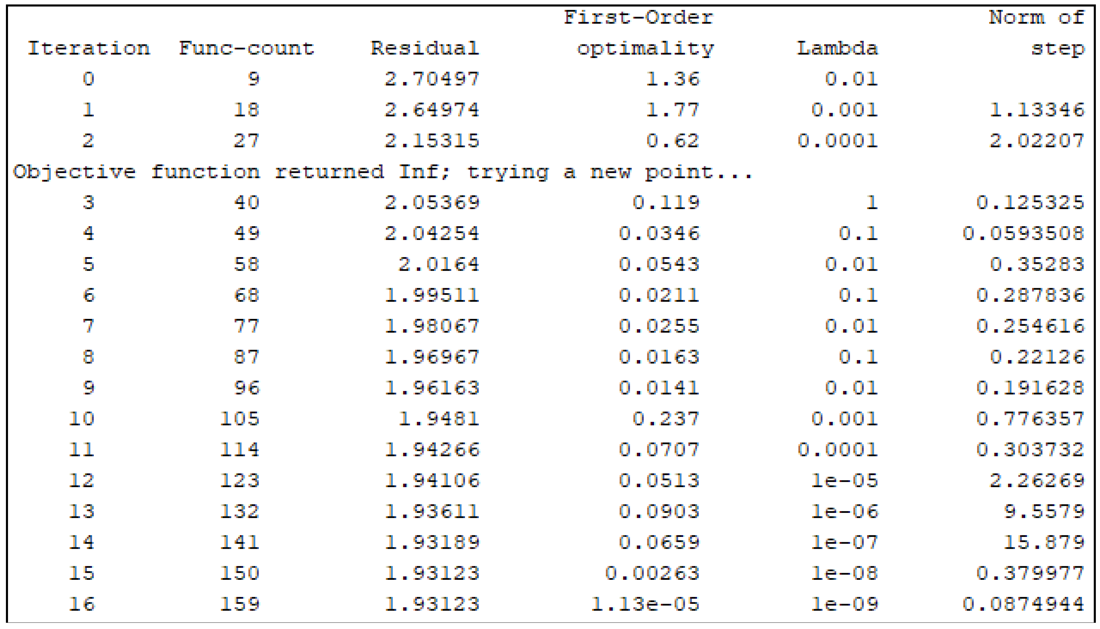
Although several stopping criteria, such as absolute function criterion, sequence convergence criterion, maximum iteration count criterion, and so on, can be adopted, here, the algorithm stops when the final change in the sum of squares relative to its initial value is less than the default value of the function tolerance. One must remember that although the algorithm ensures optimal performance, convergence to the global minimum of the objective function cannot be guaranteed. To realize the LM algorithm based on the NLS method, a MATLAB/Simulink environment is used. Termination tolerance for both the objective function and the parameter estimation is appropriately selected.
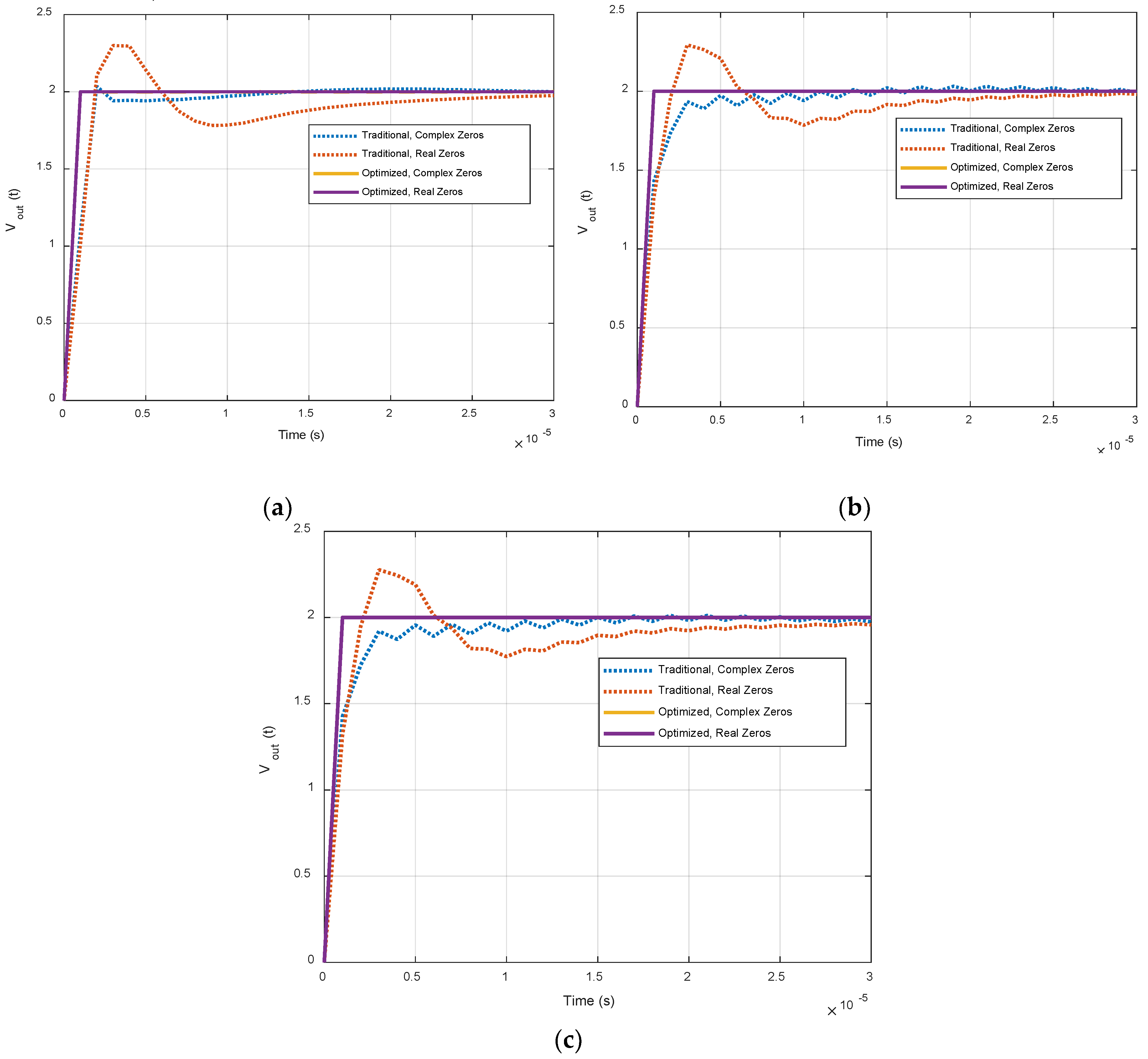
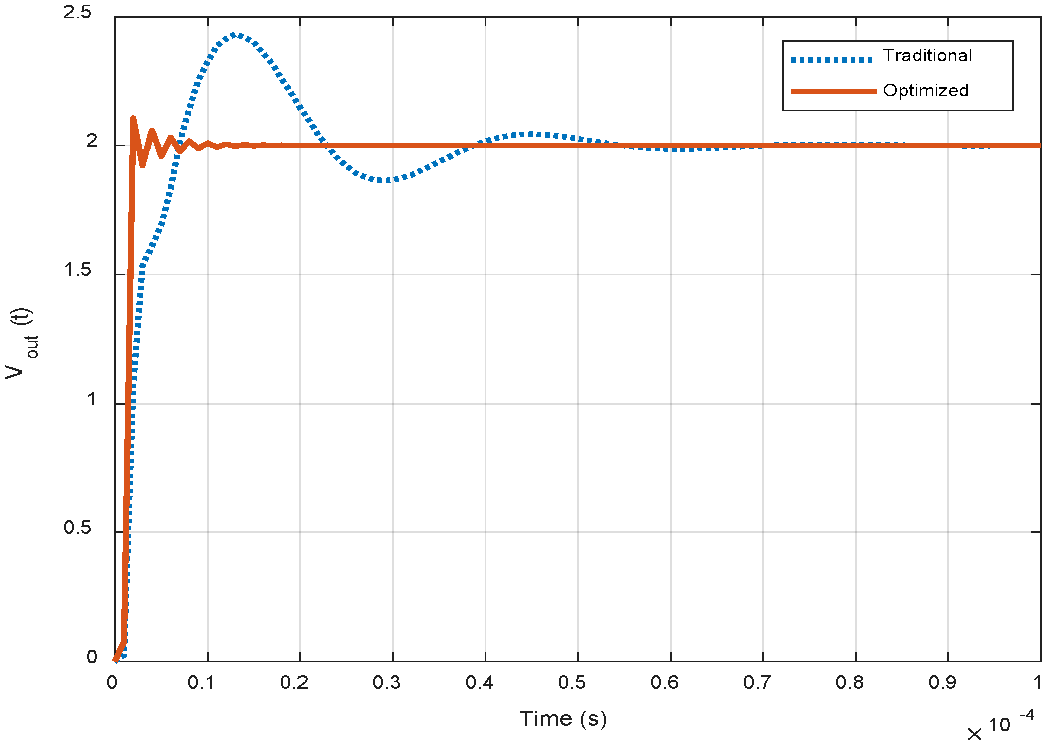
When the NLS method is applied to retune the coefficients of the digital controllers, tremendous improvement in performance is observed. All the controllers, traditional and optimized, in transfer function form, are summarized in Table 2. Correspondingly, step response characteristics displayed by all the controllers, traditional and optimized, are shown in Figure 8. The performance parameters in the form of maximum overshoot, settling time, and rise time, computed from the step response characteristics, are summarized and compared in Table 3. From Table 3, it is inferred that the optimized digital controllers offer much-improved performance as compared to their traditional counterparts. This validates the applicability and workability of the NLS method.
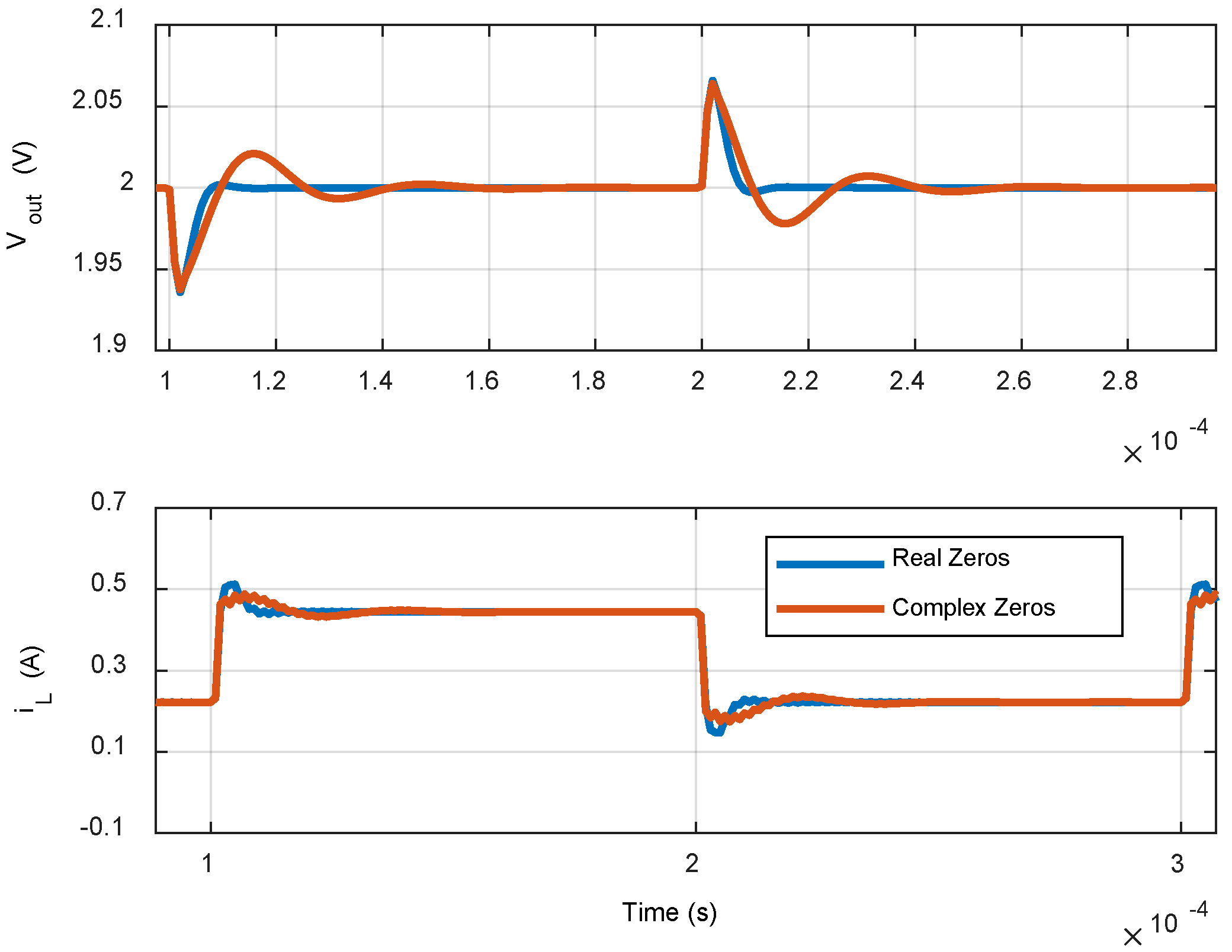
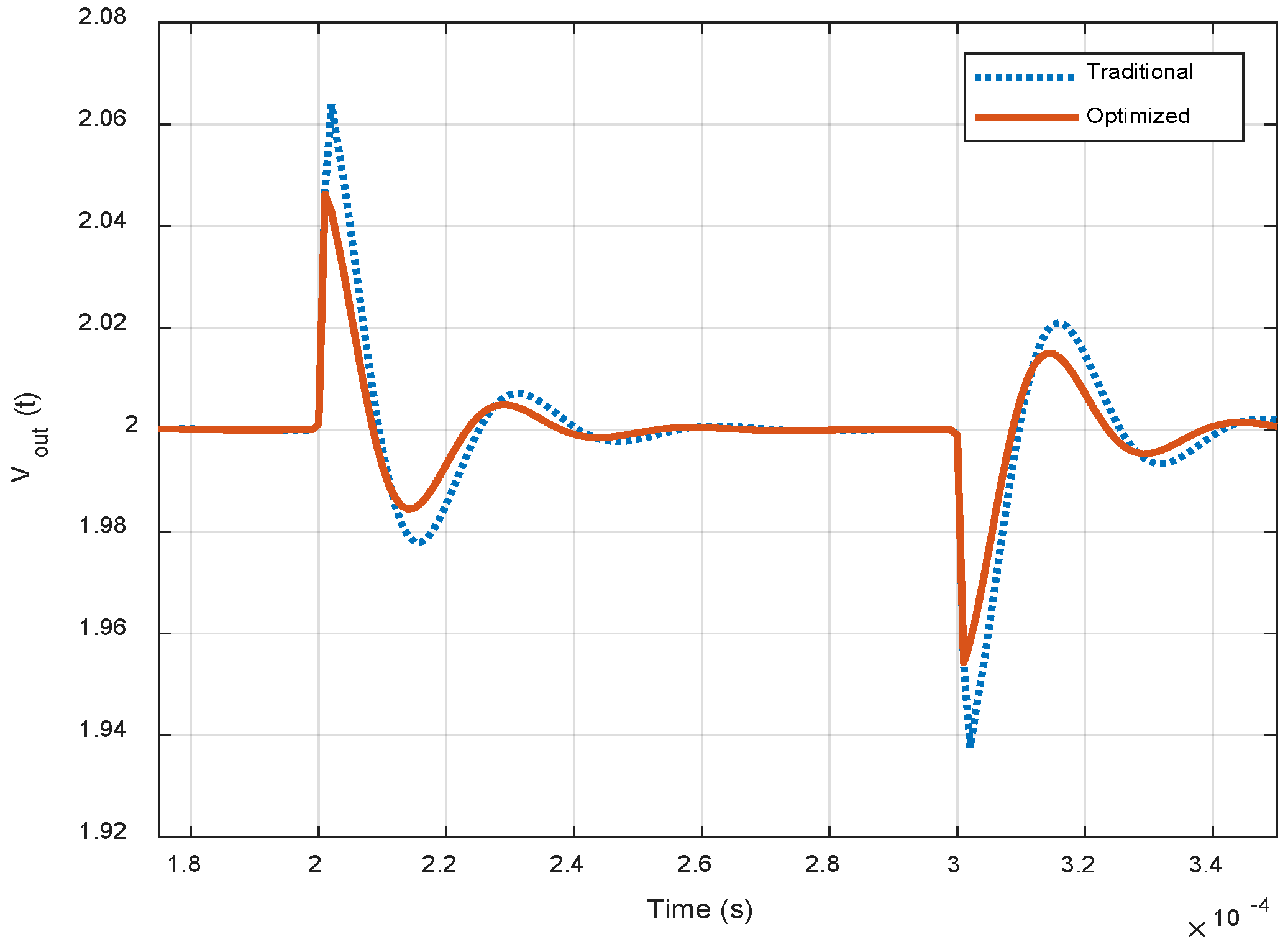
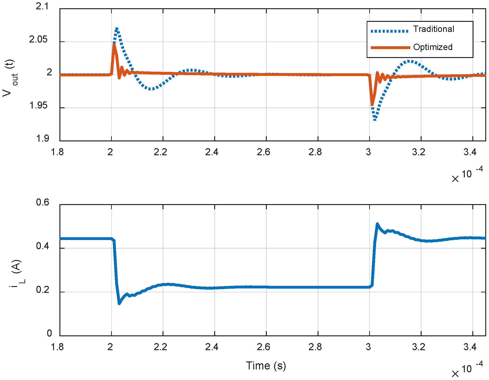
Like the step response characteristics, the optimized controllers also offer superior transient behavior. A three-pole two-zero (complex)-based optimized digital controller offers reduced recovery time and peak-to-peak spike voltage at the time of load transient as compared to its traditional form (see Figure 9). In the same way, other optimized controllers also show fast transient response with regard to their unoptimized counterparts.
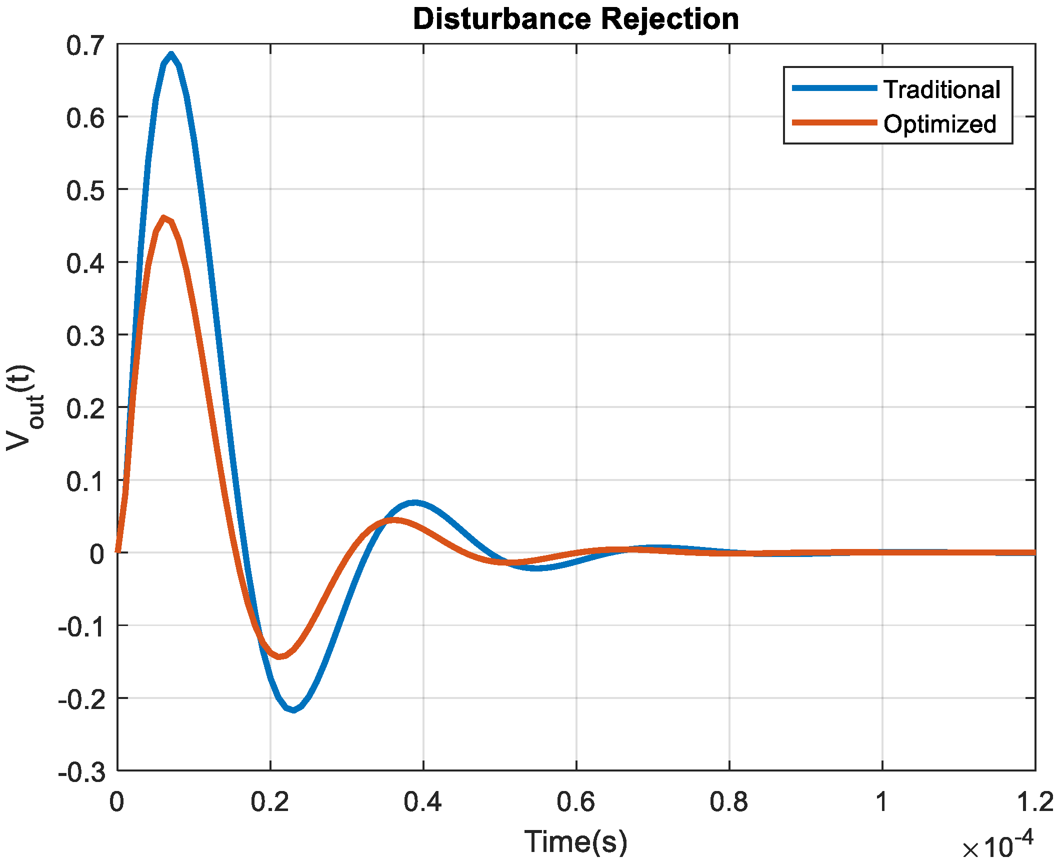
The optimized controller not only offers excellent set-point tracking and load regulation characteristics, but also exhibits improved disturbance rejection abilities against the disturbance (due to variations in the converter power-stage parameters because of aging or model uncertainties) injected at the converter input (see Figure 10).
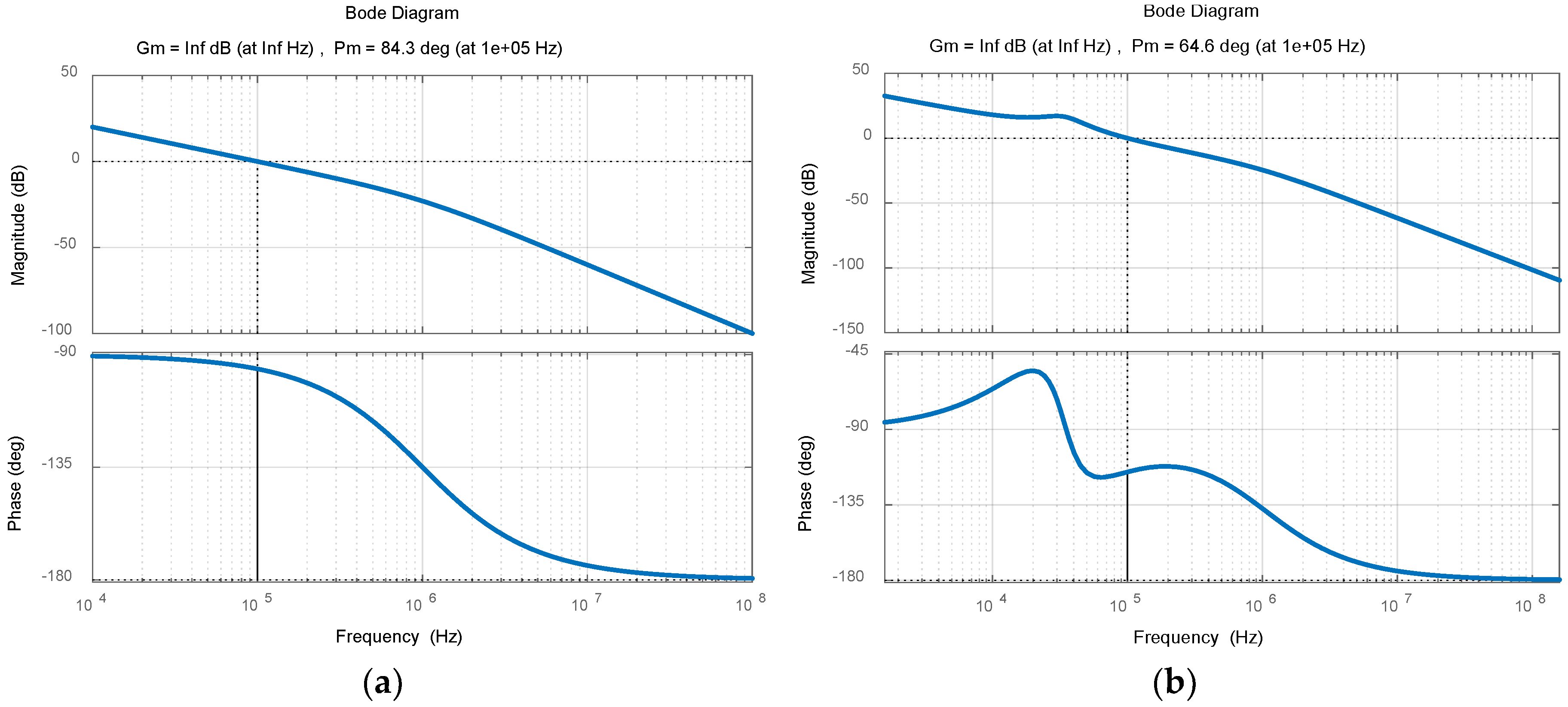
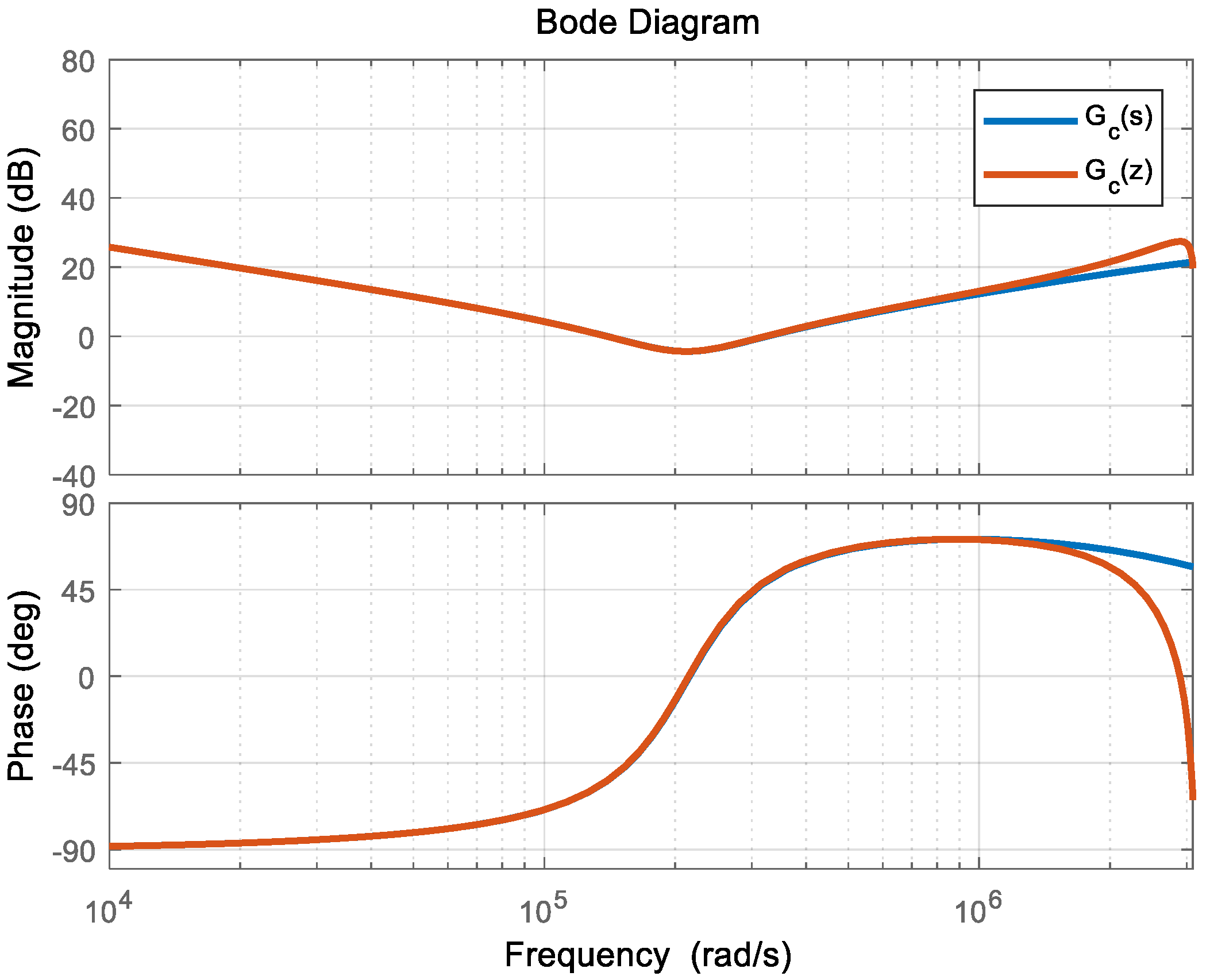
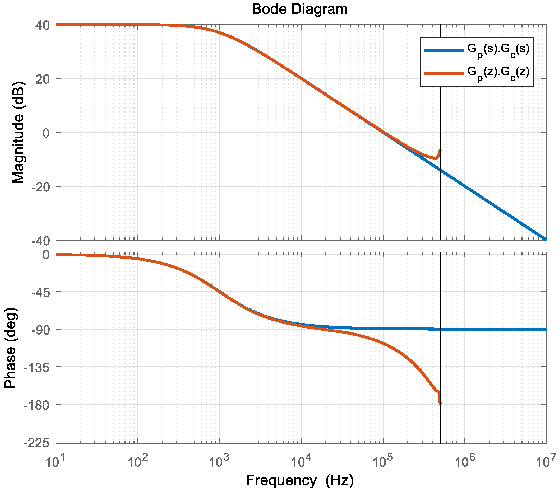
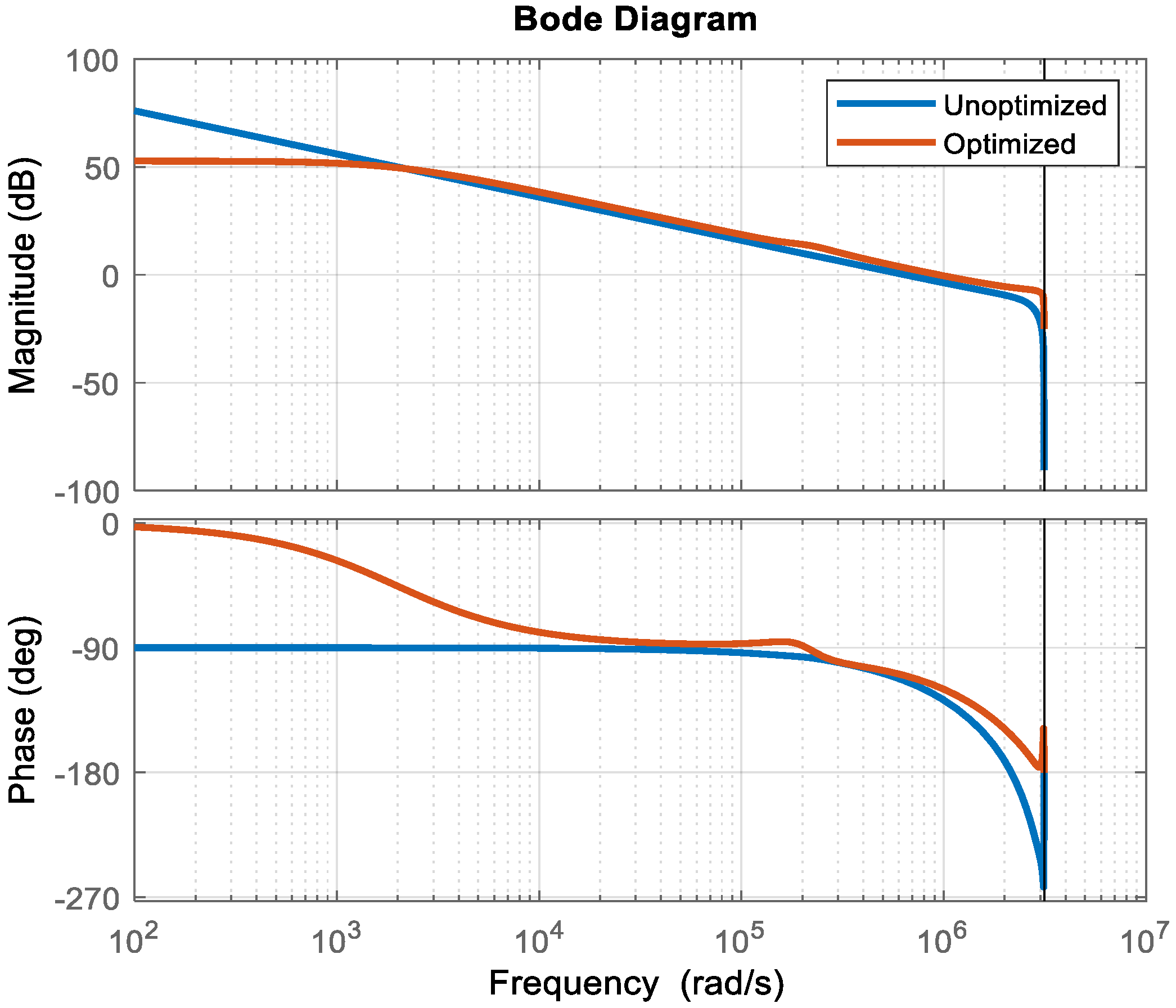
To gain more insight into the performance in terms of frequency-domain characteristics, the Bode plot of the unoptimized and optimized G p ( z ) . G c ( z ) of case 1 shown in Figure 11 clearly depicts that the optimized digital controller assists in ensuring more phase margin (and thus system stability) for all the frequencies, as compared to the unoptimized digital controller.
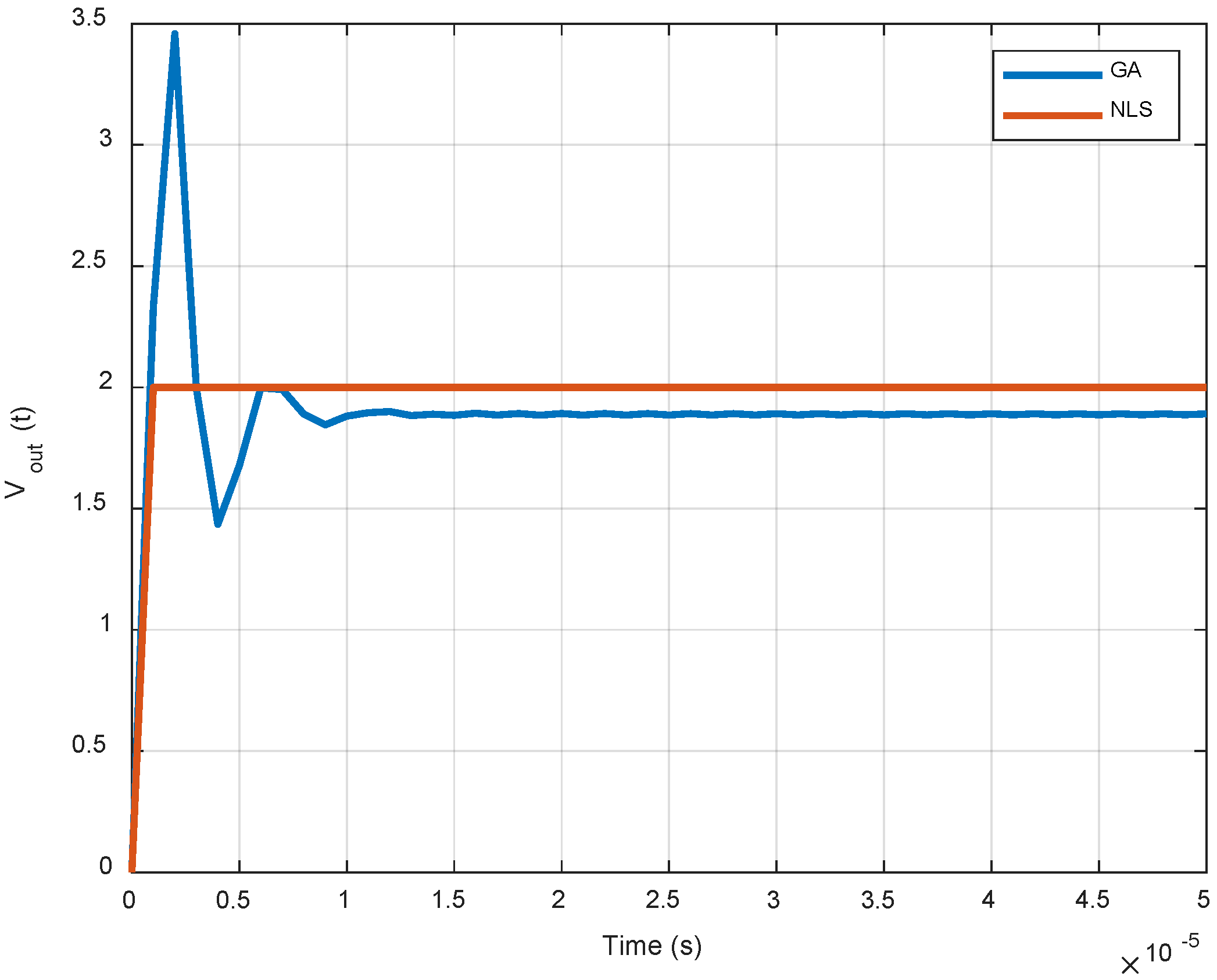
In order to validate the superiority of the proposed NLS method over the other optimization techniques, such as a genetic algorithm (GA), a comparison of the voltage response of the two-pole two-zero (complex)-based optimized digital controllers obtained through NLS and GA is presented in Figure 12. For the typical design example, the NLS method completely outshines GA performance-wise (overshoots, steady-state error, etc.). The GA parameters considered are the following: objective function = Integral Time Absolute Error (ITAE), population size = 200, generations = 25, crossover fraction = 0.65, and function tolerance = 1 × 10⁻⁶.

5. Digital Control Loop Elements Modelling

A digital control loop involves mixed signals. A continuous-time error signal digitized through the ADC is processed by the digital controller. The discrete-time controller output signal is then converted into the analog one through the DAC/DPWM to apply on–off pulses to the switching circuit. For the more realistic digitally compensated buck converter system, inherently existing nonlinearities occurring in the digital control loop should be modelled and considered.

5.1. Loop Delay

The digital control loop suffers from the delay introduced by various elements in the loop. The delay due to the ADC conversion time t A D C , the digital controller processing time t P , the DAC conversion time t D A C , the gate-driver propagation delay t G D , and so forth constitutes the total loop delay t d , which adversely limits the loop bandwidth, thus resulting in deteriorated performance. However, the effect becomes less prominent if the loop delay remains within the one sampling period T s . With the availability of high-speed ADCs, DACs, processors, and FPGAs, the total loop delay can be reduced. A delay of half the period, i.e., td = 0.5 µs, is considered in the design examples. The delay can be modelled mathematically by e s t d 1 + ( 1 + s t d ) , where the first-order lag approximation has been used to make the calculations simpler.

5.2. ADC and DAC Resolutions

In order to avoid unwanted oscillations, called limit cycle oscillations (LCOs), and thus to ensure steady-state behavior, ADC and DAC resolutions should be selected with care. Regarding the ADC resolution, LCOs can be avoided if the output error voltage is restricted within the allowed output voltage variation ΔVout. Alternatively, the ADC quantization step calculated by q v , A D C = V max / 2 n A D C should be lesser in value than ΔVout, i.e.,
( 1 H ) ( V max 2 n A D C ) Δ V o u t ( V max 2 n A D C 1 V o u t ) ( Δ V o u t V o u t V r e f V o u t ) ,   with   H = V r e f V o u t
Manipulation of Equation (42) gives the formula for ADC resolution n A D C as follows [27]:
n A D C int [ log 2 ( V max V r e f V o u t Δ V o u t ) ]
where V max , V o u t , and V r e f represent the maximum output, output, and reference voltages, respectively; H signifies the scaling factor for the sensed output voltage and is set to one for concerned design examples; the function int [] refers to the upper rounded integer value of the argument.
Without going into the mathematical detail, it has been observed experimentally that the DPWM resolution, n D P W M , should be finer than that of the ADC, n A D C . Mathematically,
n D P W M int [ n A D C + log 2 ( V r e f V max D ) ]
In Equation (44), addition of the term log 2 ( V r e f / V max D ) to n A D C indicates that n D P W M should at least be set one bit larger than n A D C in the steady state. This corresponds two DPWM levels to one ADC level.
Numerically, assuming the maximum ripples do not exceed 1% of the output voltage (the design specification considered for the design example) and V r e f to be 80% of V max , the minimum resolution required by the ADC is 7 bits. The quantization step q v , A D C for the error signal ranging from −1 to +1 (ADC’s dynamic range), thus, is calculated to be 2/27 = 0.0156. The n D P W M is, then, 8 bits. ADC and DPWM gains, being dependent on their resolutions, computed through K A D C = 2 n A D C and K D P W M = 1 / ( 2 n D P W M 1 ) respectively, are calculated to be 128 and 1/255, respectively.

6. Redesigning and Optimizing the Digital Controller

In order to compensate all the additionally incorporated effects in the digital control loop due to the inclusion of delay and ADC and DAC gains, the digital controller has to be resigned. More specifically, the controller has to be redesigned for the modified plant described by
G p ( s ) = e s t d G v d ( s ) K A D C K D P W M
Following the same procedure as described above, a three-pole two-zero (complex)-based digital controller (instead of using all the controllers for saving space) for the modified plant G p ( s ) is given by
G c ( z ) = 14.1 z 3 11.68 z 2 13.51 z + 12.27 z 3 + 0.4273 z 2 0.9566 z 0.4707
On the optimization of this digital controller through the nonlinear least squares method, somewhat deviated coefficients are observed this time. The optimized digital controller for the modified plant comes out to be
G c ( z ) = 16.7824 z 3 25.6728 z 2 + 9.2157 z 0.0464 0.3731 z 3 + 0.0796 z 2 0.4081 z 0.0446
Once the algorithm is run, as can be seen from Figure 13, with the progression of iterations, the residual decreases monotonically, thus ensuring the better set-point tracking. This certifies the fine-tuning of the digital controller coefficients by the NLS method. The algorithm stops when the final change in the sum of squares relative to its initial value is less than the default value of the function tolerance.

7. Additional Numerical Simulations

For the sake of investigating the effectiveness of the proposed optimized digital controllers, some additional simulation results for the digital control loop incorporating the delay and ADC and DAC gains using the MATLAB/Simulink environment are presented. A solver of the fixed-step type is used. The loop delay is considered to be half the switching period. ADC and DPWM gains are set to 128 and 0.0039, respectively. The step response offered by the three-pole two-zero (complex)-based unoptimized and optimized digital controllers described in Equations (46) and (47), respectively, for the modified plant described in Equation (45) is shown in Figure 14.
From the step response offered by the controllers, it is depicted that the optimized controller offers better static performance characteristics as compared to its unoptimized form (see Table 4).
In addition, at the time of transient, the response takes much less time to recover to its steady-state value with a controlled peak spike. For example, for a load current change of 0.44 A to 0.22 A and then from 0.22 A to 0.44 A, the optimized controller shows less recovery time as well as reduced voltage peak-to-peak spike with regard to its traditional form (see Figure 15). Simulation results reveal that the digital controllers are well-retuned by the NLS method and offer superior static and dynamic performance.

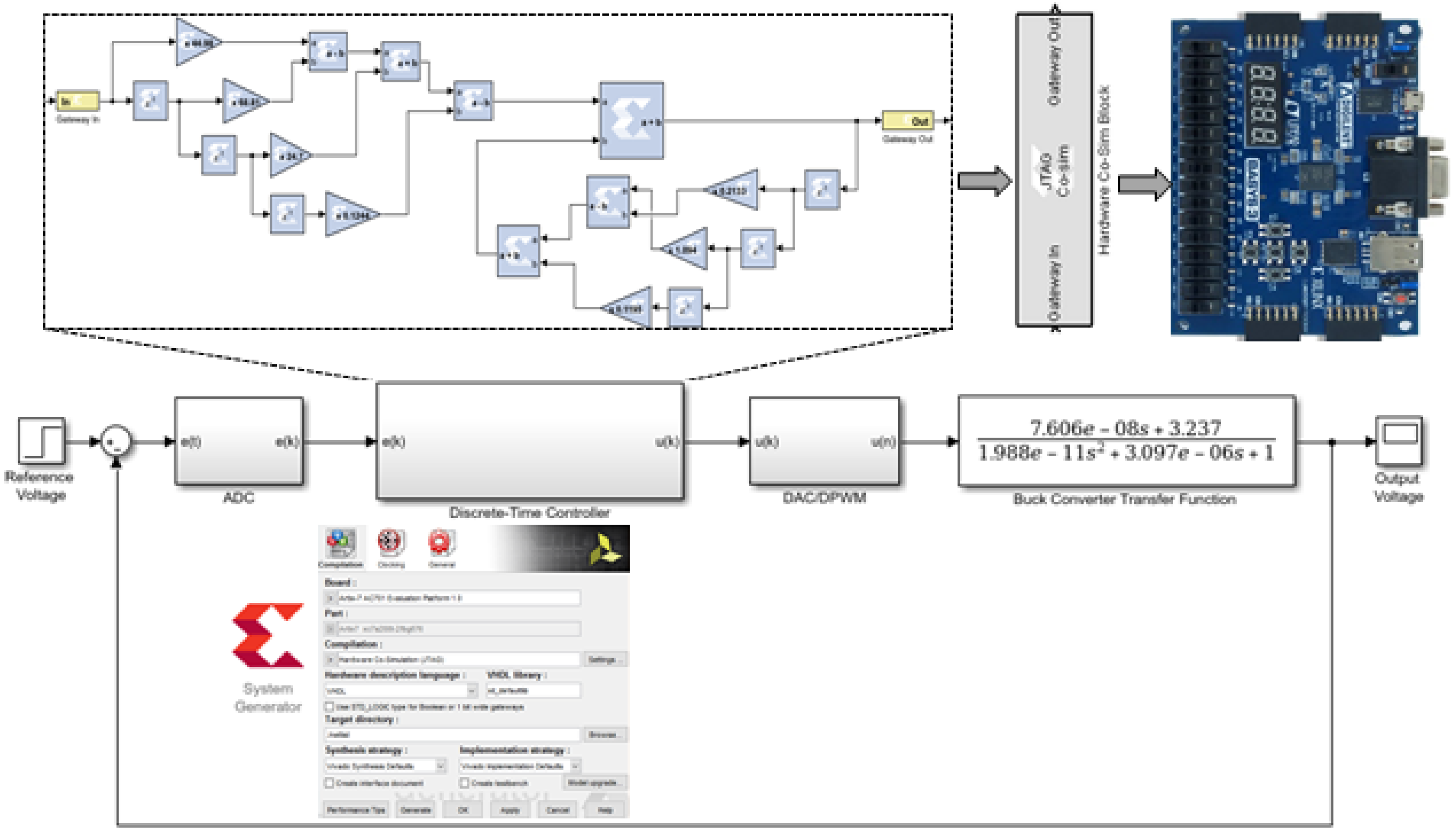
8. Rapid Hardware-in-the-Loop (HiL) Implementation

The Simulink plugged-in architecture-level design tool named Xilinx System Generator (XSG), for DSP from Xilinx, is employed for the implementation of a digital control algorithm on a high-speed, high-end, and high-density Basys 3 Artix-7 FPGA board after automatically generating portable, synthesizable, and vendor-neutral VHDL code. XSG automatically invokes both the Core Generator and ChipScope generator to construct the netlist and cores, and thus the configuration bitstream, once the target device/FPGA XC7A35T-1CPG236C from Xilinx, Inc. (an American technology company) and the compilation target (Hardware Co-Simulation JTAG) are set in its settings. High-level abstractions produced by a control design engineer in the Simulink model are translated into the low-level and executable VHDL code through the bitstream. FPGAs can be easily interfaced with Simulink through the XSG environment. This enables control design engineers to build sophisticated digital control algorithms quickly, with respect to the traditional Resistor-Transistor Logic (RTL) development times without having the knowledge of VHDL language, and then implement it on an FPGA, thus shortening the design and testing time.
The optimized digital controller described in Equation (47) can be expressed equivalently in the standard form as follows:
G c ( z ) = 44.9810 68.8094 z 1 + 24.7003 z 2 0.1244 z 3 1 + 0.2133 z 1 1.0938 z 2 0.1195 z 3
Equation (48) can be translated into the difference equation through the inverse Z-transform as follows:
u ( k ) = 44.9810 e ( k ) 68.8094 e ( k 1 ) + 24.7003 e ( k 2 ) 0.1244 e ( k 3 ) 0.2133 u ( k 1 ) + 1.0938 u ( k 2 ) + 0.1195 u ( k 3 )
The above controller difference equation realized using hardware-realizable blocks from the XSG library is shown in Figure 16. The controller coefficients are realized using a single precision floating-point data type characterized by the word lengths of 32 bits. A new hardware cosimulation library and thus a synthesizable block (which is to be downloaded into the Artix-7 board) are automatically generated (see Figure 16) on the successful generation of VHDL code. The JTAG cosimulation block is the equivalent representation of the previously used XSG simulation blocks, including the gateway-in and gateway-out blocks used for the realization of digital control algorithms. JTAG communication between a hardware platform (Artix-7 FPGA board) and Simulink (on PC) for a supported board is carried out for downloading the bitstream. In this way, a JTAG-based hardware cosimulation is performed by downloading the Vivado program-based generated bit file into the FPGA, thereby closing the loop.
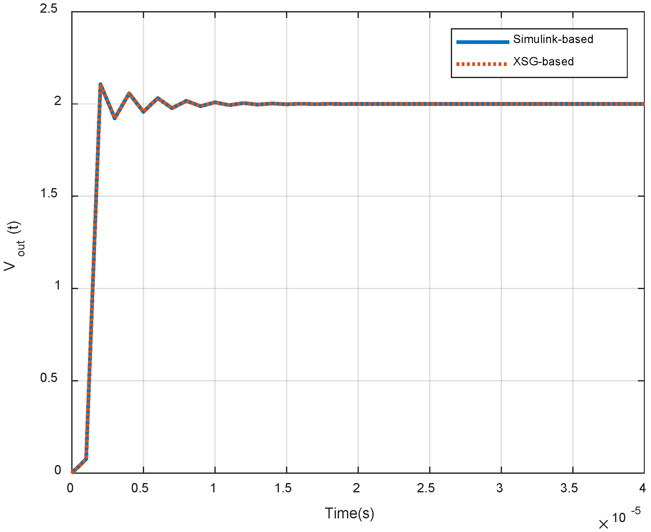
Careful analysis of the step response shown in Figure 17 depicts that the XSG-based compensated system displays almost the same performance as the Simulink-based compensated system. This is due to the fact that XSG uses the floating-point data format for the realization of controller coefficients, just like Simulink, which utilizes ‘double’ type data. Set time-steps for the hardware implementation, rounding and truncation errors, and the sampling issues associated with the digital systems may cause slight performance deterioration in the XSG-based system. The bit-true and cycle-true characteristic of the XSG makes the numerical simulations such as if they were attained through the real hardware implementation.

9. Conclusions

In this paper, optimization of the PZC technique-based digital controllers through the NLS method is performed to enhance the static and dynamic performance. In the proposed control methodology, which is essentially a digital redesign or emulation technique, the analog compensators with complex and real zeros designed on the basis of the PZC technique are mapped into the digital compensators by using a bilinear transformation technique with an appropriate sampling period. Discrete-time approximation of continuous-time controllers, even when accomplished through using the ‘best’ Tustin transformation, introduces frequency distortion. Although low analog frequencies are relatively well-mapped into the same digital frequencies, high frequencies result in highly nonlinear mapping. As a result, the performance of the digital controllers deteriorates. The coefficients of the digital controllers are retuned through the NLS optimization method to enhance their performance. There occur also opportunities for improvement in compensator performance, as the placing of the compensator’s real or complex zeros in the vicinity of the plant’s poles ensures only nominal performance. Numerical results reveal that NLS-based optimized digital controllers exhibit superior static and dynamic performance as compared to the conventional (unoptimized) digital controllers, thus validating the effectiveness of the NLS optimization method. When comparing their performance, the NLS method outshines metaheuristic techniques such as GA. Rapid HiL implementation of the compensated buck converter system is also successfully performed.

Author Contributions

G.A., J.G., U.F., M.I.A., A.R. and M.U.A. suggested the idea, performed the simulations and experiments, and managed the paper. V.E.B. and M.E.B. assisted in the idea development and paper writing.

Funding

This research received no external funding.

Conflicts of Interest

The authors declare no conflict of interest.

References

  1. Chen, N.; Wei, T.; Shang, K.; Wang, R. Digital controller based on delta operator for high-frequency DC–DC switching converters. IET Power Electron. 2018, 11, 1224–1230. [Google Scholar] [CrossRef]
  2. Abe, S.; Ogawa, M.; Zaitsu, T.; Obata, S.; Shoyama, M.; Ninomiya, T. Dynamic characteristics improvement of digital controlled DC-DC converter by means of PZC control. In Proceedings of the 2010 IEEE International Conference on Industrial Technology, Vina del Mar, Chile, 14–17 March 2010; pp. 750–755. [Google Scholar]
  3. Abe, S.; Ogawa, M.; Zaitsu, T.; Obata, S.; Shoyama, M.; Ninomiya, T. Frequency response improvement of DSP controlled DC-DC converter with pole-zero cancellation technique. In Proceedings of the INTELEC 2009—31st International Telecommunications Energy Conference, Incheon, Korea, 18–22 October 2009; pp. 1–6. [Google Scholar]
  4. Abe, S.; Ogawa, M.; Zaitsu, T.; Obata, S.; Shoyama, M.; Ninomiya, T. Investigation of parameter tolerance on digitally controlled DC-DC converter with pole-zero-cancellation technique. In Proceedings of the 2010 IEEE Asia Pacific Conference on Circuits and Systems, Kuala Lumpur, Malaysia, 6–9 December 2010; pp. 476–479. [Google Scholar]
  5. Abbas, G.; Farooq, U.; Gu, J.; Asad, M.U. Controller design for low-input voltage switching converters having non-minimum phase characteristics. In Proceedings of the 2015 IEEE 28th Canadian Conference on Electrical and Computer Engineering (CCECE), Halifax, NS, Canada, 3–6 May 2015; pp. 1294–1298. [Google Scholar]
  6. Chang, Y.-T.; Lai, Y.-S. Digital controller design for buck converter with the reduction of phase transition and output voltage oscillation under transient state. In Proceedings of the 2008 4th IET Conference on Power Electronics, Machines and Drives, York, UK, 2–4 April 2008; pp. 376–380. [Google Scholar]
  7. Kittipeerachon, K.; Bunlaksananusorn, C. Feedback compensation design for switched mode power supplies with a right-half plane (RHP) zero. In Proceedings of the Second International Conference on Power Electronics, Machines and Drives (PEMD 2004), Edinburgh, UK, 31 March–2 April 2004; Volume 1, pp. 236–241. [Google Scholar]
  8. Veerachary, M. Digital Controller Design for Low Source Current Ripple Fifth-Order Boost Converter. IEEE Trans. Ind. Electron. 2014, 61, 270–280. [Google Scholar] [CrossRef]
  9. Ghosh, A.; Banerjee, S.; Sarkar, M.K.; Dutta, P. Design and implementation of type-II and type-III controller for DC–DC switched-mode boost converter by using K-factor approach and optimisation techniques. IET Power Electron. 2016, 9, 938–950. [Google Scholar] [CrossRef]
  10. Mercader, P.; Åström, K.J.; Baños, A.; Hägglund, T. Robust PID Design Based on QFT and Convex–Concave Optimization. IEEE Trans. Control Syst. Technol. 2017, 25, 441–452. [Google Scholar] [CrossRef]
  11. Abbas, G.; Farooq, U.; Gu, J.; Asad, M.U.; Abid, M.I. Optimization of discrete-time controller applied to DC-DC step-down converter. In Proceedings of the 2015 International Conference on Emerging Technologies (ICET), Peshawar, Pakistan, 19–20 December 2015; pp. 1–5. [Google Scholar]
  12. Velasco, F.J.; Revestido, E.; López, E.; Moyano, E.; Casado, M.H. Techniques for Tuning Track-keeping Controllers of an Autonomous in-scale Fastferry Model. Int. J. Syst. Appl. Eng. Dev. 2008, 2, 227–236. [Google Scholar]
  13. Huber, J.E.; Korn, A.J. Optimized Pulse Pattern modulation for Modular Multilevel Converter high-speed drive. In Proceedings of the 2012 15th International Power Electronics and Motion Control Conference (EPE/PEMC), Novi Sad, Serbia, 4–6 September 2012; pp. LS1a-1.4-1–LS1a-1.4-7. [Google Scholar]
  14. Kumar, A.; Rafi, S.M.; Singh, G.K. A hybrid method for designing linear-phase quadrature mirror filter bank. Digit. Signal Process. 2012, 22, 453–462. [Google Scholar] [CrossRef]
  15. Song, Z.; Xia, C.; Liu, T. Predictive Current Control of Three-Phase Grid-Connected Converters with Constant Switching Frequency for Wind Energy Systems. IEEE Trans. Ind. Electron. 2013, 60, 2451–2464. [Google Scholar] [CrossRef]
  16. Zheng, Y.; Peng, S. A Practical Roadside Camera Calibration Method Based on Least Squares Optimization. IEEE Trans. Intell. Transp. Syst. 2014, 15, 831–843. [Google Scholar] [CrossRef]
  17. Altintop, Ç.G.; Şentürk, T.; Latifoğlu, F. Diagnosis of epileptic seizure from EEG signals by least squares method. In Proceedings of the 2017 Medical Technologies National Congress (TIPTEKNO), Trabzon, Turkey, 12–14 October 2017; pp. 1–4. [Google Scholar]
  18. Mu, B.; Bai, E.-W.; Zheng, W.X.; Zhu, Q. A globally consistent nonlinear least squares estimator for identification of nonlinear rational systems. Automatica 2017, 77, 322–335. [Google Scholar] [CrossRef] [Green Version]
  19. Wu, Z.; Yuan, J.; Zhang, J.; Huang, H. A hierarchical face recognition algorithm based on humanoid nonlinear least-squares computation. J. Ambient Intell. Hum. Comput. 2016, 7, 229–238. [Google Scholar] [CrossRef]
  20. Zhang, M.; Li, X.; Liu, J.; Su, H. Dual-mode LQR-feedforward optimal control for non-minimum phase boost converter. IET Power Electron. 2017, 10, 92–102. [Google Scholar] [CrossRef]
  21. Vorperian, V. Simplified Analysis of PWM Converters Using the Model of the PWM Switch: Parts I and II. IEEE Trans. Aerosp. Electron. Syst. 1990, 26, 490–505. [Google Scholar] [CrossRef]
  22. Tian, S.; Lee, F.C.; Li, Q.; Yan, Y. Unified Equivalent Circuit Model and Optimal Design of V2 Controlled Buck Converters. IEEE Trans. Power Electron. 2016, 31, 1734–1744. [Google Scholar] [CrossRef]
  23. Johansson, B. DC-DC Converters, Dynamic Model Design and Experimental Verification. Ph.D. Thesis, Department of Industrial Electrical Engineering and Automation, Lund University, Lund, Sweden, 2004. [Google Scholar]
  24. Hsia, T.-H.; Tsai, H.-Y.; Lin, Y.-Z.; Chen, D.; Chang, W.-H. Digital compensation of a high-frequency voltage—Mode DC-DC converter. In Proceedings of the 2007 European Conference on Power Electronics and Applications, Aalborg, Denmark, 2–5 September 2007; pp. 1–8. [Google Scholar]
  25. Madsen, K.; Nielsen, N.B.; Tingleff, O. Methods for Nonlinear Least Squares Problems; Technical Report, Informatics and Mathematical Modeling; Technical University of Denmark: Lyngby, Denmark, 2004. [Google Scholar]
  26. Marquardt, D.W. An algorithm for least-squares estimation of nonlinear parameters. J. Soc. Ind. Appl. Math. 1963, 11, 431–441. [Google Scholar] [CrossRef]
  27. Huang, M.; Lu, Y.; Sin, S.; Seng, P.; Martins, R.P.; Ki, W. Limit Cycle Oscillation Reduction for Digital Low Dropout Regulators. IEEE Trans. Circuits Syst. II Express Briefs 2016, 63, 903–907. [Google Scholar] [CrossRef]
Figure 1. Closed-loop (digital) control system block diagram.
Electronics 07 00412 g001
Figure 2. AC small-signal equivalent circuit for the buck converter power stage.
Electronics 07 00412 g002
Figure 3. Flow chart explaining the design procedure adopted for the various cases. PZC: pole-zero-cancellation.
Electronics 07 00412 g003
Figure 4. Bode plot of the open-loop compensated system using (a) the complex zeros and (b) the real zeros.
Electronics 07 00412 g004
Figure 5. Load regulation by real and complex zeros-based compensators.
Electronics 07 00412 g005
Figure 6. Bode diagram of the compensators.
Electronics 07 00412 g006
Figure 7. Bode plot of the open-loop compensated buck converter system.
Electronics 07 00412 g007
Figure 8. Step response offered by (a) case 1, (b) case 2, and (c) case 3 controllers.
Electronics 07 00412 g008
Figure 9. Load transient response.
Electronics 07 00412 g009
Figure 10. Disturbance rejection comparison.
Electronics 07 00412 g010
Figure 11. Bode plot of the unoptimized and optimized G p ( z ) G c ( z ) .
Electronics 07 00412 g011
Figure 12. Output voltage response of the optimized digital controllers.
Electronics 07 00412 g012
Figure 13. Iterative process offered by the nonlinear least squares (NLS) method.
Electronics 07 00412 g013
Figure 14. Controllers’ output voltage response.
Electronics 07 00412 g014
Figure 15. Response of the controllers against the changes in load current.
Electronics 07 00412 g015
Figure 16. Hardware-in-the-loop (HiL) implementation of the compensated buck converter system.
Electronics 07 00412 g016
Figure 17. Output voltage response obtained through the Simulink and Xilinx System Generator (XSG)-based compensated system.
Electronics 07 00412 g017
Table 1. Buck converter transfer function.
ConverterTransfer FunctionDescription
Analog 7.606 × 10 8 s + 3.237 1.988 × 10 11 s 2 + 3.097 × 10 6 s + 1 A two-pole, one-zero converter, having complex conjugate poles at 105 × (−0.7787 ± j2.1031) with Q = 1.44
Digital 0.07288   z + 0.06332 z 2 1.827 z + 0.8692 Discretized form obtained using ZOH with Ts = 1 µs
Table 2. Controllers’ transfer functions.
Case No.Compensator ZerosAnalog Controller Gc(s)Digital Controller Gc(z)Optimized Digital Controller Gc(z)
1Complex 4.309 × 10 6 s 2 + 0.6041 s + 1.951 × 10 5 3.74 × 10 15 s 3 + 1.827 × 10 7 s 2 + s 6.753 z 3 5.595 z 2 6.47 z + 5.877 z 3 + 0.4273 z 2 0.9566 z 0.4707 6.8515 z 3 5.5501 z 2 6.625 z + 5.8584 0.5529 z 3 + 0.4746 z 2 0.5528 z 0.4707
Real 3.597 × 10 6 s 2 + 1.378 s + 1.303 × 10 5 3.74 × 10 15 s 3 + 1.827 × 10 7 s 2 + s 6.257 z 3 4.072 z 2 6.069 z + 4.261 z 3 + 0.4273 z 2 0.9566 z 0.4707 5.7210 z 3 4.3870 z 2 5.8969 z + 5.1035 0.4617 z 3 + 0.4163 z 2 0.4644 z 0.4135
2Complex 4.288 × 10 6 s 2 + 0.6011 s + 1.941 × 10 5 2.35 × 10 8 s 2 + s 8.858 z 2 16.2 z + 7.71 z 2 0.08978 z 0.9102 8.9562 z 2 16.2048 z + 7.6637 0.7227 z 2 0.1018 z 0.6209
Real 3.512 × 10 6 s 2 + 1.495 s + 1.59 × 10 5 2.35 × 10 8 s 2 + s 8.213 z 2 13.27 z + 5.358 z 2 0.08978 z 0.9102 7.4178 z 2 13.4213 z + 6.3473 0.5986 z 2 0.0843 z 0.5143
3Complex 6.825 × 10 10 s 2 + 9.567 × 10 5 s + 30.9 3.74 × 10 12 s 2 + 1.592 × 10 4 s + 1 8.831 z 2 16.15 z + 7.686 z 2 0.08352 z 0.9045 8.9287 z 2 16.155 z + 7.6401 0.7205 z 2 0.1015 z 0.6190
Real 5.59 × 10 10 s 2 + 23.79 × 10 5 s + 25.31 3.74 × 10 12 s 2 + 1.592 × 10 4 s + 1 8.187 z 2 13.23 z + 5.341 z 2 0.08352 z 0.9045 7.3954 z 2 13.3807 z + 6.3281 0.5968 z 2 0.0841 z 0.5127
Table 3. Comparative analysis of controllers’ performance characteristics.
Case No.ControllerPerformance Parameters
Max. Overshoot (%)Rise Time (µs)Settling Time (µs)
1Traditional, Complex Zeros1.77891.56748.5697
Traditional, Real Zeros14.98541.522825.322
Optimized, Complex Zeros0.05360.800.98
Optimized, Real Zeros0.0000040.800.98
2Traditional, Complex Zeros1.59492.181312.02
Traditional, Real Zeros14.70281.595322.31
Optimized, Complex Zeros0.00550.790.97
Optimized, Real Zeros0.000050.800.98
3Traditional, Complex Zeros0.55602.243514.103
Traditional, Real Zeros13.82121.610824.22
Optimized, Complex Zeros0.00290.7990.979
Optimized, Real Zeros4.1280 × 10−100.800.98
Table 4. Comparison of performance characteristics.
Performance CharacteristicsDigital ControllerOptimized Digital Controller
Rise Time (s)4.5888 × 10−67.8825 × 10−7
Settling Time (s)4.7043 × 10−55.0295 × 10−6
Overshoot (%)21.64575.3088
(First) Peak (V)2.43292.1062
Peak Time (s)1.30 × 10−52.00 × 10−6

