Article

Parameter Identification of DC-DC Converters under Steady-State and Transient Conditions Based on White-Box Models

by
Jordi-Roger Riba
1,*,
Manuel Moreno-Eguilaz
2,
Santiago Bogarra
1 and
Antoni Garcia
1
1
Department of Electric Engineering, Universitat Politècnica de Catalunya, Rambla Sant Nebridi 22, 08222 Terrassa, Spain
2
Department of Electronic Engineering, Universitat Politècnica de Catalunya, Rambla Sant Nebridi 22, 08222 Terrassa, Spain
*
Author to whom correspondence should be addressed.
Electronics 2018, 7(12), 393; https://doi.org/10.3390/electronics7120393
Submission received: 9 November 2018 / Revised: 26 November 2018 / Accepted: 28 November 2018 / Published: 5 December 2018
(This article belongs to the Special Issue Advanced Power Conversion Technologies)

Abstract

:
This paper proposes a white-box approach for identifying the parameters of DC-DC buck and boost switch mode power converters. It is based on discretizing the differential equations that describe the dynamic behavior of the converters. From the discretized equations and experimental data, the parameters of the converters are identified, thus obtaining both the values of the passive components and the transfer function coefficients of the controller. To this end, steady state and transient experimental signals are analyzed, including the input and output voltages and the inductor and output currents. To determine the accuracy of the proposed method, once the parameters are identified, a simulation with the identified parameters of the converter is run and compared with experimental signals. Such results show the accuracy and feasibility of the approach proposed in this work, which can be extended to other converters and electrical and electronic devices.

1. Introduction

Switch mode power converters (SMPC) are broadly applied in different areas, including motor drives, computers, portable electronics [1], domestic appliances [2], or in power conversion systems for renewable generation [3], among others. They have appealing characteristics such as compactness and high conversion efficiency [4].
Parameter identification comprises a set of techniques for estimating the most suitable values of the parameters that govern a dynamical system based on data from the observed behavior of the system. This approach has been applied in different areas, including transmission lines [5], synchronous generators [6] or modelling of capacitors [7] among others. Parameter identification is a powerful tool to develop fault diagnosis approaches for power converters based on continuously observing the values of passive components, since changes in these values due to ageing or deterioration can lead to power converter failure [8]. Power converter modelling has been traditionally based on identifying the parameters of single power converters, instead of modelling multi power converter systems. Currently, sectors such as avionics, aerospace or naval, are integrating complex power systems comprising numerous generators, motors or different types of power converters. Such complex systems habitually integrate different SMPCs from several manufacturers, which often disclose limited data of the inner parameters. The information that the engineers can gather from datasheets is limited and not detailed enough to generate exhaustive models; the application of parameter identification approaches can solve this issue. Therefore, in many cases design engineers cannot know the values of all SMPC’s components beforehand [9]. Instead, the input and output currents and voltages of the SMPC can be measured.
In addition, conventional methods for modeling power converter involve a thorough analysis of the power converter configuration. Different inaccuracy sources such as poor load description, sudden external disturbances, tolerances, ageing of key components or diverse ambient conditions may alter the behavior of the power converter throughout its lifetime. By applying a system identification approach, these changes can be detected and taken into account [10].
Parameter identification comprehends a set of techniques aimed at reproducing the dynamic behavior of a system from experimental data [11]. However, due to the complexity of real systems, the difficulty in producing realistic models, and the wide range of operating conditions, this is still a challenging problem. Parameter identification focuses on identifying or estimating the different parameters of the model from experimental measurements when the system operates under steady-state or transient conditions. Parameter identification is often based on white-box models. White-box models assume that the structure of the system is totally known, thus building theoretical models from a set of differential equations describing the behavior of the system accurately [12,13]. The main advantage of this approach is that it allows retrieving from experimental data the values of the parameters in which the physical model of the system is based. However, excessively detailed models may be unacceptable in terms of required computational load [14].
Parameter identification has been applied to identify parameters of electrical machines and circuits operating under dynamic conditions by analyzing electrical signals such as current and voltage [15]. Parameter identification can be performed online or offline, either in the time or frequency domains. According to the technical literature, different strategies can be applied for parameter identification in SMPCs. Gietler et al. [16] identified the values of the passive components of a buck converter from the time-discrete transfer function of such electronic device using state space models. Ahmeid et al. [2] proposed to identify the whole transfer function of a buck converter by means of a Kalman Filter. Linares-Flores et al. [17] presented a design of a generalized proportional–integral adaptive controller for boost converters based on the an algebraic parameter identification approach. This approach required dealing with a simplified white-box model of the converter. Chen et al. performed an online identification of inductor parameters in a boost converter by injecting a small signal in order to produce a transient state, and applying an observer obtained from the capacitor current [18]. Xu et al. [19] proposed to applying an optimization approach for reducing the computational burden to estimate SMPC’s parameters by applying recursive algorithms. Ru and Gong [20] proposed a parameter identification method for boost power converters SMPC based on recursive least squares arithmetic and wavelet denoising. Buiatti et al. [21] estimated the parameters of different power converters from continuous time models of such converters, where the time derivatives of the signals were performed by means of polynomial interpolation. Although in the abovementioned works accurate results were obtained, some values such as the parameters of the proportional-integral-derivative (PID) controller were, in general, not identified.
In this paper a parametric identification of DC-DC buck and boost SMPC is carried out from experimental data, based on a white-box model. To this end the experimental input and output voltages and inductor and output currents are acquired and used as input signals for parameter identification, jointly with the white-box model of the analyzed SMPC. Whereas the parameters of the capacitor (capacitance and equivalent series resistance or ESR), the inductor (inductance and series resistance) as well as the equivalent resistance of the switches are identified from the steady state response, the parameters of the controller are identified from the transient response when an additional load is suddenly connected in parallel with the load. Moreover, the models presented in this work integrate the experimental signals instead of calculating the time derivatives, due to the numerical issues of the later ones. Experimental results presented in this work prove that the values of the passive components of the analyzed SMPC can be correctly identified, including the parameters of the controller and the equivalent resistance of the switches, this being one of the contributions of this work. Although the proposed approach is applied in DC-DC buck and boost SMPC, it can be extended to other types of converters and power devices.

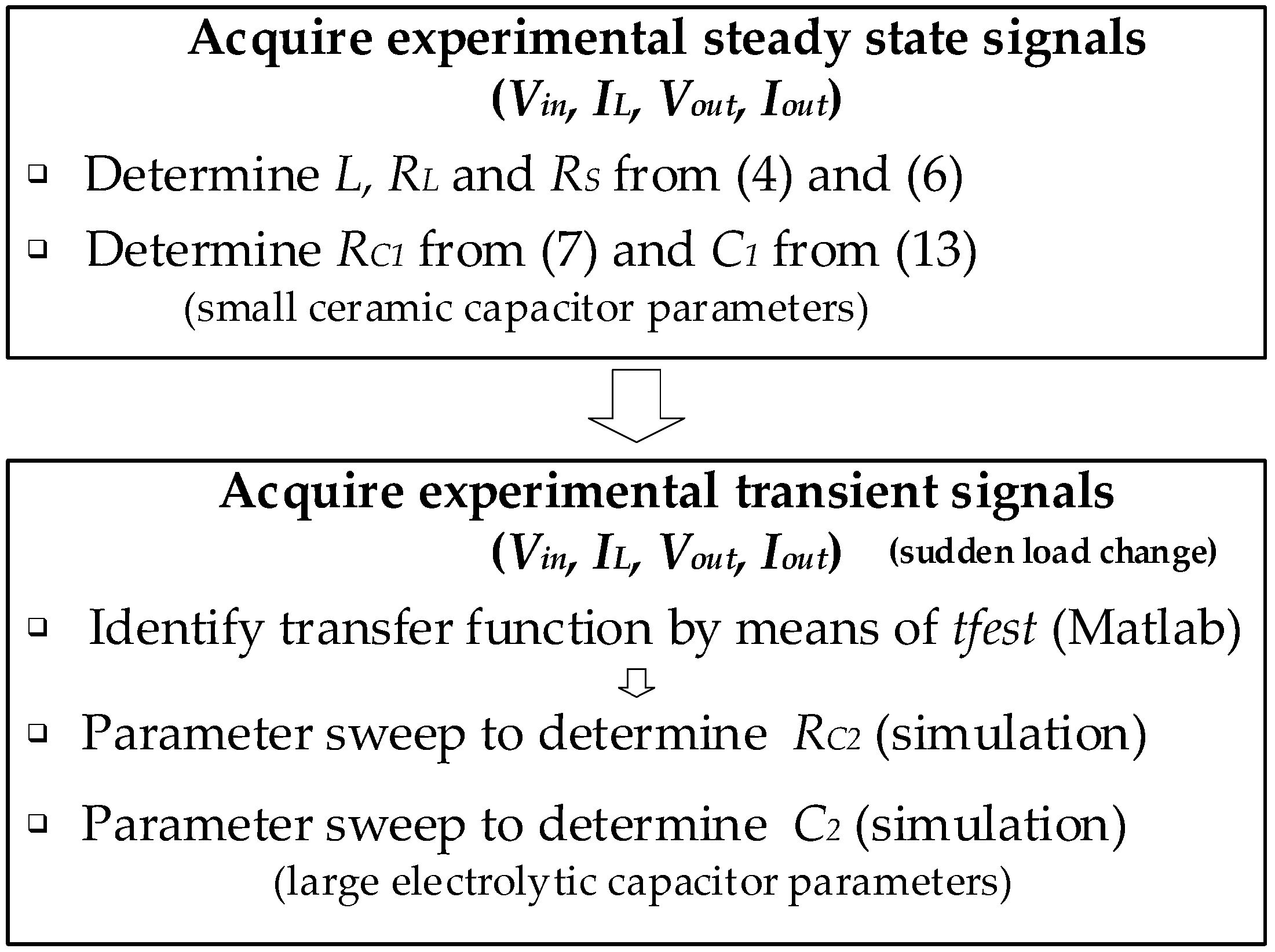
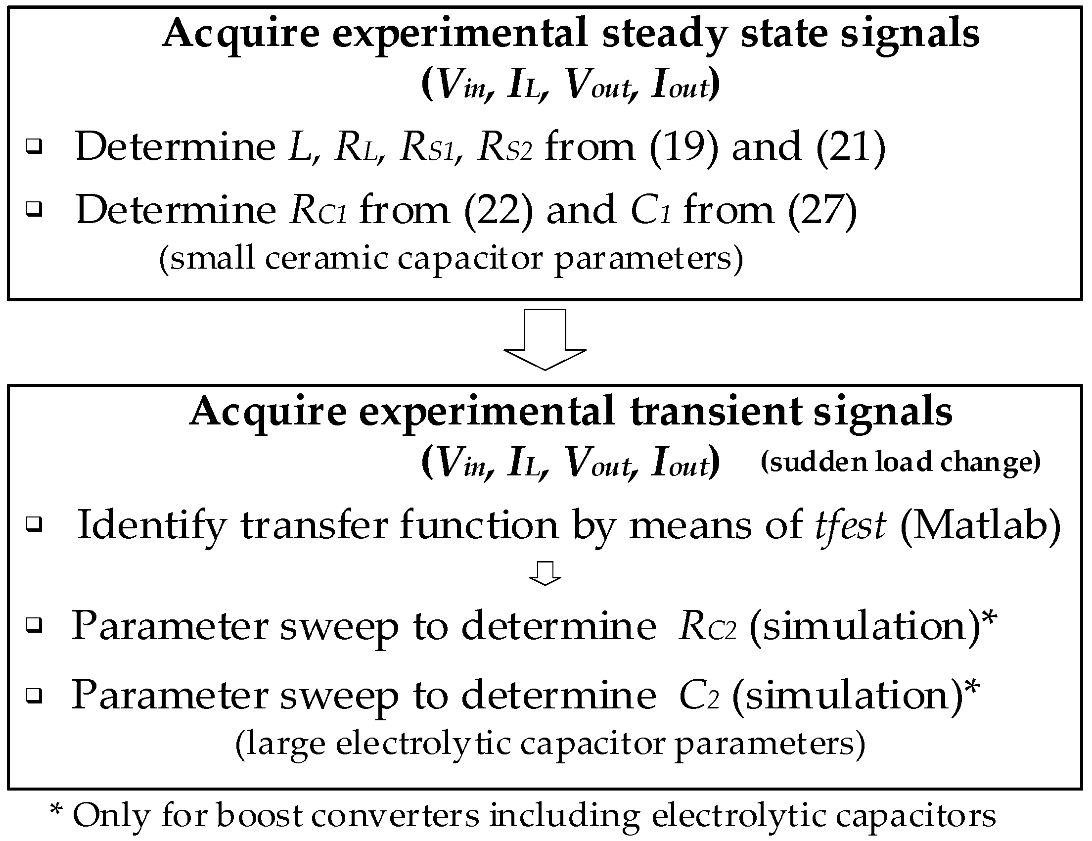
2. The Proposed Parameter Identification Method

This section develops the approach proposed in this work to identify the parameters of the buck and boost converters dealt with in this paper. Whereas the values of the inductor (inductance L and series resistance RL), the capacitor (capacitance C and series resistance RC) and the resistance of the switch are identified from steady state signals (input and output voltages, inductor current and output current), the coefficients of the transfer function of the control circuit are identified based on transient signals (input and output voltages and inductor and output currents).

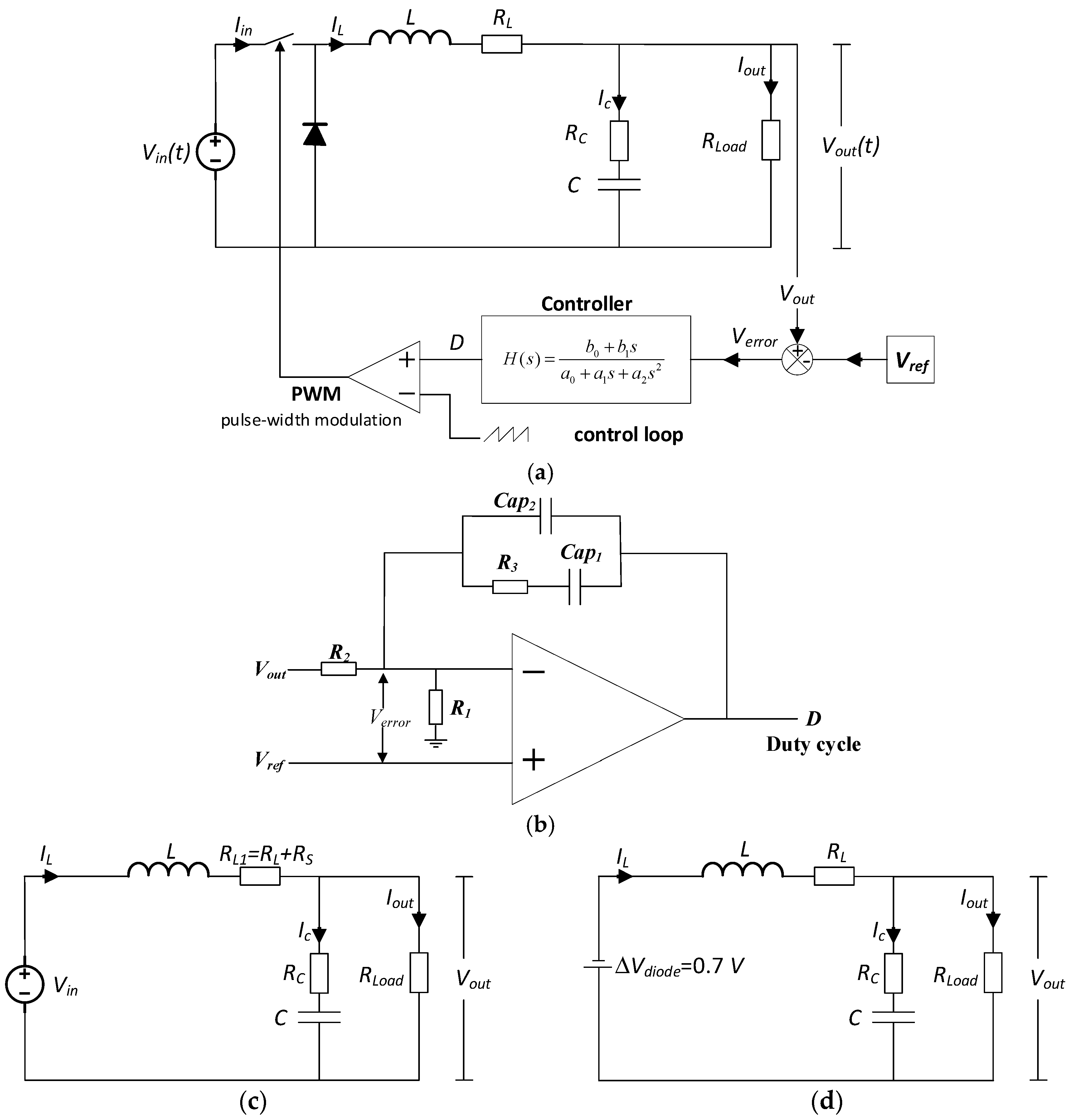
2.1. Buck Converter Parameter Identification

Figure 1 shows the model of the buck converter dealt with in this work, including the control loop. The parameters to identify are the passive components L, RL, C, RC, RS (switch resistance) and the coefficients of the control loop b1, a1 and a2. It is noted that D is the duty cycle.
It is worth noting that although Figure 1 only depicts one capacitor in parallel with the load, commercial SMPC habitually include several parallel connected capacitors to ensure the converter performs appropriately. These capacitors usually are grouped in two types, i.e., capacitors of large and low capacitances. Depending on type and size of the capacitor (ceramic, electrolytic, polymer, tantalum, etc.), the response in steady state and transient state may change. An important parameter determining such behavior is the capacitor equivalent series resistance (ESR). When large electrolytic capacitors are combined with small ceramic capacitors, the output capacitors can be modelled by an equivalent large electrolytic capacitor connected in parallel to a smaller ceramic one. They are meant to adjust the ripple and transient response separately. The ESR of the small capacitor affects the output voltage ripple, whereas the ESR of the larger one affects the overall stability, that is, the time constant under transient conditions. Although SMPC manufacturers sometimes provide the ESR of electrolytic capacitors, they often do not provide the ESR of ceramic capacitors, so it must be obtained from experimental data.
To identify the passive components values of the buck converter, that is, L, RL, C, RC and RS, the steady state response is analyzed, since it is almost not affected by the controller. To this end the model of the converter during TON is analyzed in detail, that is, when the switch is in its ON state.
The L and RL1 = RL + Rs values can be calculated as follows,
V i n V o u t = I L R L 1 + L d I i n d t
and next (1) is integrated.
d I L = ( V i n / L ) d t ( V o u t / L ) d t ( R L 1 / L ) I L d t
Equation (2) can be discretized by considering two discrete time instants T1 and T2 = T1 + ΔT, ΔT being the discrete time step considered. Once discretized, the trapezoidal rule allows calculating the integral, thus obtaining (3).
I L , T 2 I L , T 1 = ( T 2 T 1 ) 2 L [ V i n , T 2 V o u t , T 2 + V i n , T 1 V o u t , T 1 ) ( I L , T 2 + I L , T 1 ) R L 1 ]
Finally, L and RL1 can be obtained by means of the following equations system, which considers four time instants T1, T2 = T1 + ΔT, T3 = T2 + ΔT, T4 = T3 + ΔT.
[ I L , T 2 I L , T 1 I L , T 4 I L , T 3 ] = [ ( V i n , T 2 V o u t , T 2 + V i n , T 1 V o u t , T 1 ) ( T 2 T 1 ) 2 ( I L T 2 I L , T 1 ) ( T 2 T 1 ) 2 ( V i n , T 4 V o u t , T 4 + V i n , T 3 V o u t , T 3 ) ( T 4 T 3 ) 2 ( I L , T 4 I L , T 3 ) ( T 4 T 3 ) 2 ] [ 1 L R L 1 L ]
Similarly to (1), the equations governing the dynamic behavior during the OFF state can be expressed as in (5).
Δ V d i o d e V o u t = I L R L + L d I L d t
Therefore, the solution is similar to (4), so it can be expressed as in (6).
[ I L , T 2 I L , T 1 I L , T 4 I L , T 3 ] = [ ( Δ V d i o d e , T 2 V o u t , T 2 Δ V d i o d e , T 1 V o u t , T 1 ) ( T 2 T 1 ) 2 ( I L , T 2 I L , T 1 ) ( T 2 T 1 ) 2 ( Δ V d i o d e , T 4 V o u t , T 4 Δ V d i o d e , T 3 V o u t , T 3 ) ( T 4 T 3 ) 2 ( I L , T 4 I L , T 3 ) ( T 4 T 3 ) 2 ] [ 1 L R L L ]
It is noted that RL1 = RL + RS is calculated during the ON state, RS being the ON resistance of the switch (see Figure 1a). Since RL is calculated during the OFF state, the switch resistance can be obtained by applying RS = RL1RL.
Once the parameters of the inductor and the switch are known, those of the capacitor must be obtained. According to [21], the ESR of the output capacitor in a buck converter can be calculated as,
R c = Δ V o u t R l o a d Δ I L R l o a d Δ V o u t
Δ V o u t and Δ I L being, respectively, the output voltage and current ripples. During TON, the inductor current can be written as,
I L = C d V c d t + I o u t
whereas the voltage in the capacitor is expressed as in (9).
V c = V o u t ( I L I o u t ) R c
By replacing (8) into (9) and integrating, it results in (10).
C d V c = ( I L I o u t ) d t
Equation (8) can be discretized by considering two discrete time instants T1 and T2, where T2 = T1 + ΔT, ΔT being the discrete time step considered. Once discretized, the trapezoidal rule allows calculating the integral, thus obtaining,
C ( V c , T 2 V c , T 1 ) = T 2 T 1 2 ( I L , T 2 I o u t , T 2 + I L , T 1 I o u t , T 1 )
and next, (9) is substituted into (11), thus obtaining (12).
C [ V o u t , T 2 ( I L , T 2 I o u t , T 2 ) R c V o u t , T 1 + ( I L , T 1 I o u t , T 1 ) R c ] = T 2 T 1 2 ( I L , T 2 I o u t , T 2 + I L , T 1 I o u t , T 1 )
By isolating the capacitance C in (12), its value is obtained as in (13).
C = T 2 T 1 2 ( I L , T 2 I o u t , T 2 + I L , T 1 I o u t , T 1 ) V o u t , T 2 ( I L , T 2 I o u t , T 2 ) R c V o u t , T 1 + ( I L , T 1 I o u t , T 1 ) R c
It is worth noting that (7) and (13) provide, respectively, the ESR and the capacitance of the smaller ceramic output capacitor, RC1 and C1, respectively, since the dynamics during steady state operation is governed by such capacitor.
The values of parameters L, RL, C, RC and RS, are calculated at every time step Ti from (4), (6), (7) and (13) under steady state conditions.
As shown in Figure 1b, commercial DC-DC converters usually include a control circuit in closed loop based on a digital or analog controller to stabilize and regulate the output voltage Vout according to Vref, the reference voltage. The relationship between the input and the output of the control circuit can be expressed by means of a transfer function. In the case of analog circuits whose transfer function has one zero and two poles (TPS40200EVM-002 non-synchronous buck converter shown in Figure 1), it can be expressed as [23],
H ( s ) = D ( s ) V e r r o r ( s ) = b 0 + b 1 s a 0 + a 1 s + a 2 s 2
where Verror is the error signal and D = TON/(TON + TOFF) the duty cycle.
The parameters ai and bi of the transfer function in (14) are estimated during transient conditions. Transients can be generated by suddenly connecting a known resistor in parallel with the load. These coefficients can be identified by using the tfest function of the system identification toolbox from Matlab [2].
As explained, some power converters include two types of output capacitors. In this case, the values of RC and C obtained in (7) and (13), correspond to the smaller capacitor, that is, RC1 and C1, respectively. To determine the ESR and the capacitance of the larger output electrolytic capacitor (RC2 and C2), an iterative approach is applied during this sudden load change. To this end, this paper proposes performing a parameter sweep of RC2 and C2 by means of PSIM (Rockville, MD, USA). This parameter sweep varies the ESR RC2 from RC1 to 50·RC1 and the capacitance C2 from C1 to 100·C1, as shown in Figure 2, which is applied in two sequential steps. In the first step the RC2 values are changed and the error between experimental and simulated results is calculated at each step, so that the value of RC2 minimizing the error between experimental and simulated results is kept. Next, with this obtained value of RC2, C2 is swept until attaining a minimum error between experimental and simulation results performed with those values of RC2 and C2.
Figure 2 shows that the transient response changes in every iteration, but the voltage ripple is almost not affected. The most suitable values of RC2 and C2 are those minimizing the error between simulated and experimental results, which is calculated as in (15).
e r r o r = M e a n ( | V o u t , exp , T i V o u t , s i m , T i V o u t , exp , T i | ) i = 1 , 2 , , n   samples
Figure 3 shows a flowchart summarizing the strategy applied to identify the parameters of the buck converter by means of the experimental signals Vin, IL, Vout and Iout.

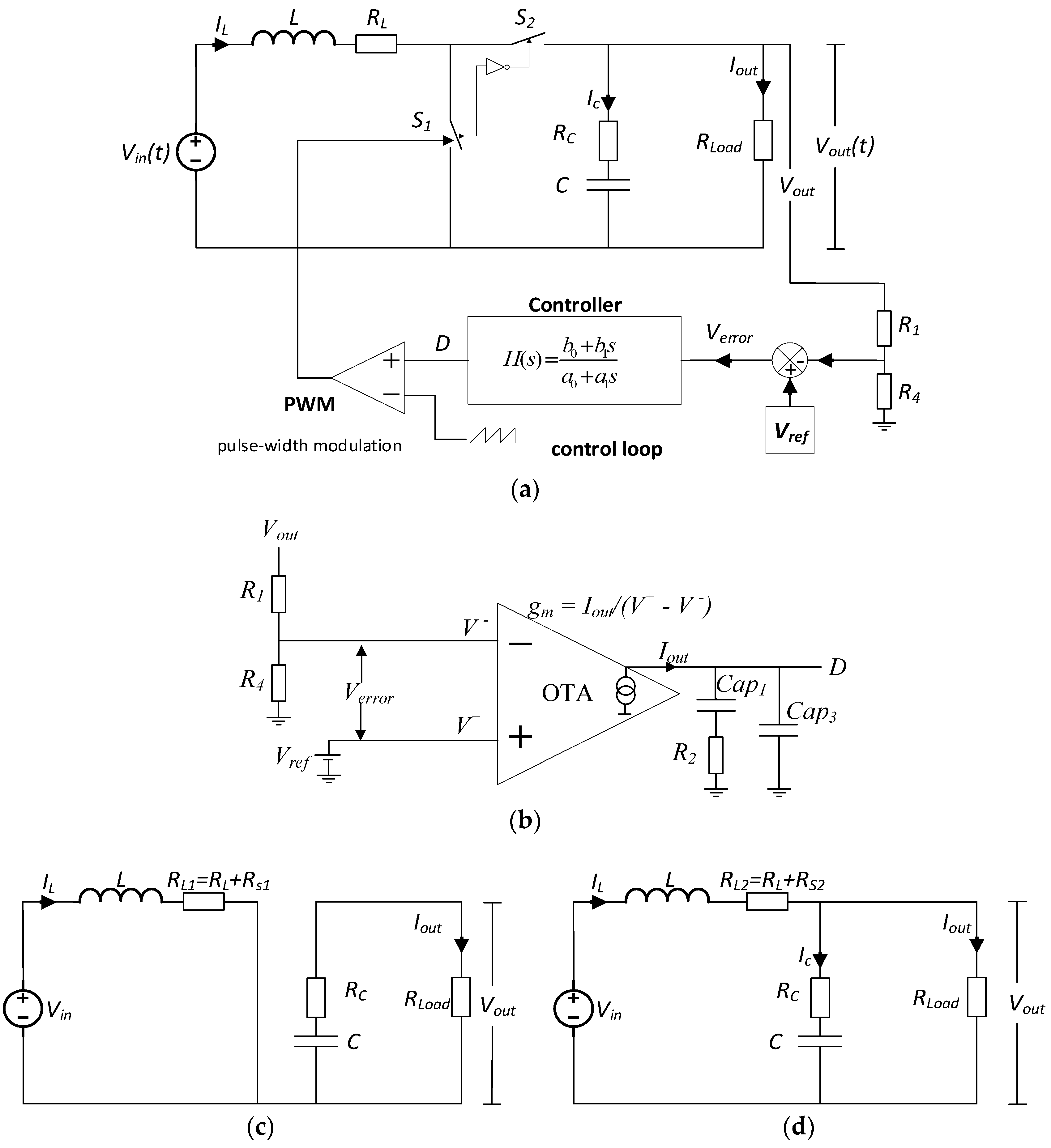
2.2. Boost Converter Parameter Identification

Figure 4 shows the model of the boost converter dealt with in this work, including the control loop. The parameters to identify are the passive components L, RL, C, RC, RS1, RS2 and the coefficients of the control loop a0, a1, b0 and b1.
As done with the buck converter, the steady state response must be analyzed to identify the passive components of the boost converter (L, RL, C, RC, RS1 and RS2), since it is almost not affected by the controller. To this end the model of the converter during TON is analyzed in detail, that is, when the switch is in its ON state.
The L and RL1 = RL + RS1 values are calculated from (16) and (17).
V i n = L d I L d t + R L 1 · I L
V i n d t = L d I L + R L 1 I L d t
By applying the trapezoidal rule of integration and considering four time instants T1, T2 = T1 + ΔT, T3 = T2 + ΔT, T4 = T3 + ΔT, (17) results in (18).
( V i n , T 2 + V i n , T 1 ) T 2 T 1 2 = L ( I L , T 2 I L , T 1 ) + ( I L , T 2 + I L , T 1 ) ( T 2 T 1 ) R L 1 2
Finally, the L and RL1 values are obtained by solving the following system of equations.
[ ( V i n , T 2 + V i n , T 1 ) T 2 T 1 2 ( V i n , T 4 + V i n , T 3 ) T 4 T 3 2 ] = [ I L , T 2 I L , T 1 ( I L , T 2 + I L , T 1 ) ( T 2 T 1 ) 2 I L , T 4 I L , T 3 ( I L , T 4 + I L , T 3 ) ( T 4 T 3 ) 2 ] [ L R L 1 ]
Similarly to (16), the equations governing the dynamic behavior during the OFF state can be expressed as in (20).
V i n V o u t = L d I L d t + R L 2 · I L
The solution is similar to (19), so it can be expressed as in (21).
[ ( V i n , T 2 + V i n , T 1 V o u t , T 2 V o u t , T 1 ) T 2 T 1 2 ( V i n , T 4 + V i n , T 3 V o u t , T 4 V o u t , T 3 ) T 4 T 3 2 ] = [ I L , T 2 I L , T 1 ( I L , T 2 + I L , T 1 ) ( T 2 T 1 ) 2 I L , T 4 I L , T 3 ( I L , T 4 + I L , T 3 ) ( T 4 T 3 ) 2 ] [ L R L 2 ]
It is noted that RL1 = RL + RS1 is calculated during the ON state, RS1 being the ON resistance of switch 1 (see Figure 4a). Similarly, RL2 = RL + RS2 is calculated during the OFF cycle, RS2 being the ON resistance of switch 2. Since there are three unknowns RL, RS1 and RS2 a third equation is required, which can be obtained by means of a suitable assumption, such as RS1 = 2RS2/3 [24].
Once the parameters of the inductor and switches are identified, the parameters of the capacitor must be obtained. According to, the ESR of the output capacitor can be calculated as [21],
R c = [ V o u t , t = 0.5 D T s w i t c h V o u t , a v e r a g e ] R L V o u t , a v e r a g e
D being the duty cycle or time period in which the inductor is charged, Tswitch is the inverse of the switching frequency, and Vout,average is the average value of the output voltage in a period Tswitch.
The currents in the equivalent circuit during TOFF accomplish (23).
I C = C d V c d t = I L I o u t C d V c = ( I L I o u t ) d t
Next, the voltage in the capacitor is calculated as,
V c = V o u t V R C = V o u t ( I L I o u t ) R c
and considering two points time instants T1 and T2 = T1 + ΔT, and applying the trapezoidal rule for approximating the integral in (23), it results in (25).
C ( V C , T 2 V C , T 1 ) = T 2 T 1 2 ( I L , T 2 I o u t , T 2 + I L , T 1 I o u t , T 1 )
Substituting VC from (24) in (25) it results in (26).
C [ V o u t , T 2 ( I L , T 2 I o u t , T 2 ) R c ( V o u t , T 1 ( I L , T 1 I o u t , T 1 ) R c ] = T 2 T 1 2 ( I L , T 2 I o u t , T 2 + I L , T 1 I o u t , T 1 )
Finally, the capacitance can be calculated from (27) by isolating C in (26).
C = T 2 T 1 2 ( I L , T 2 I o u t , T 2 + I L , T 1 I o u t , T 1 ) V o u t , T 2 ( I L , T 2 I o u t , T 2 ) R c V o u t , T 1 + ( I L , T 1 I o u t , T 1 ) R c
It is worth noting that (22) and (26) provide, respectively, the ESR and the capacitance of the smaller output capacitor, since the dynamics during steady state operation is governed by such a capacitor.
As shown in Figure 4b, as in the case of buck converters, DC-DC boost converters also include a controller to stabilize and regulate the output voltage Vout according to Vref. Therefore, a transfer function is used to describe the transient behavior of the control circuit. In the case of analog circuits whose transfer function has one zero and one pole (TPS61089EVM-742 DC-DC boost converter shown in Figure 4), it can be expressed as [23],
H ( s ) = D ( s ) V e r r o r ( s ) = b 0 + b 1 s a 0 + a 1 s
where Verror is the error signal and D = Ton/(Ton + Toff) the duty cycle.
The closed loop coefficients ai and bi in (28) are obtained by analyzing the transient data obtained by means of a fast load change caused by a sudden connection of a resistor in parallel with the load. Coefficients a0, a1, b0 and b1 will be identified by means of the tfest function of Matlab, as done in [2].
Figure 5 shows a flowchart summarizing the strategy applied to identify the parameters of the boost converter by means of the experimental signals Vin, IL, Vout and Iout.
The TPS61089EVM-742 boost converter includes four output ceramic capacitors. Therefore, the four capacitors can be modelled as equivalent ESR, RC,eq, in series with the equivalent capacitance Ceq. In this case there is no need to run a parameter sweep to determine RC2 and C2 as there is no combination of electrolytic and ceramic capacitors, so the identification of the capacitor parameters is simplified.

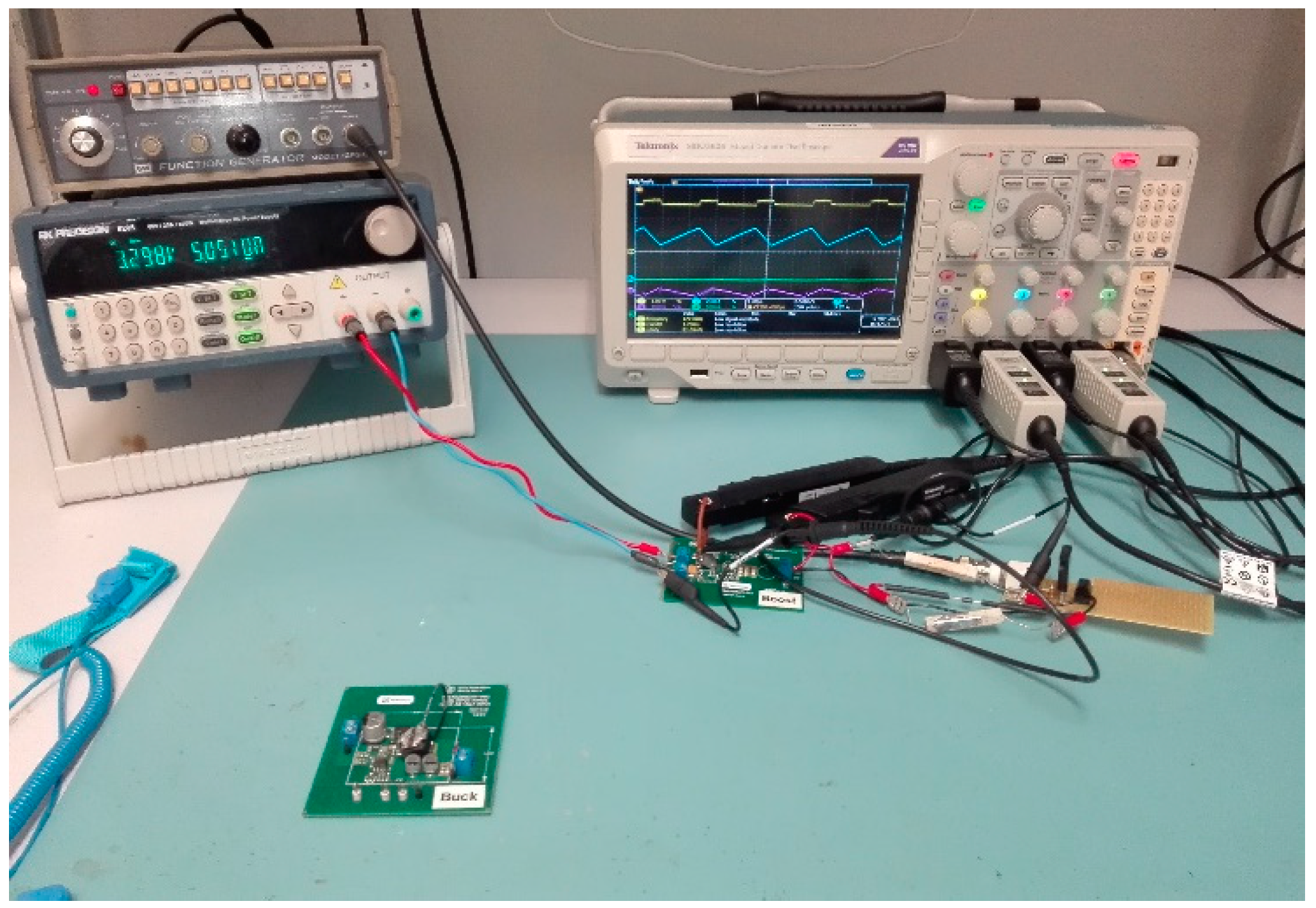
3. Experimental Results

This section summarizes the experimental results attained with the DC-DC buck and boost converters. For this purpose, the input and output voltages and inductor and output currents were acquired under steady state and transient conditions.
The non-synchronous TPS40200EVM-002 buck converter (Texas Instruments, Dallas, TX, USA) and the synchronous TPS61089EVM-742 boost converter (Texas Instruments, Dallas, TX, USA) from Texas Instruments are analyzed in this section. Experimental data were obtained from these converters. Whereas the input voltage of the TPS40200EVM-002 buck converter lies within 18–36 V, the input voltage of the TPS61089EVM-742 boost converter lies in the range of 3–5 V.
A BK Precision 9205 DC power (BK Precision Corporation, Yorba Linda, CA, USA) supply was used to supply the power converters. Currents and voltages were acquired by means of a four channel Tektronix MDO3024 (Tektronix, Beaverton, OR, USA; 200 MHz, 2.5 GS/s) digital oscilloscope with two TCP0030A current probes (Tektronix, Beaverton, OR, USA; 1 mA to 20 A, 120 MHz) and two Tektronix TPP0250 voltage probes (Tektronix, Beaverton, OR, USA; 250 MHz), as shown in Figure 6.

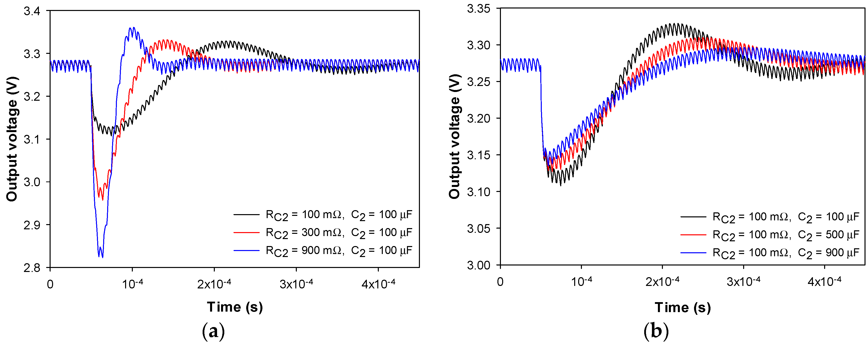
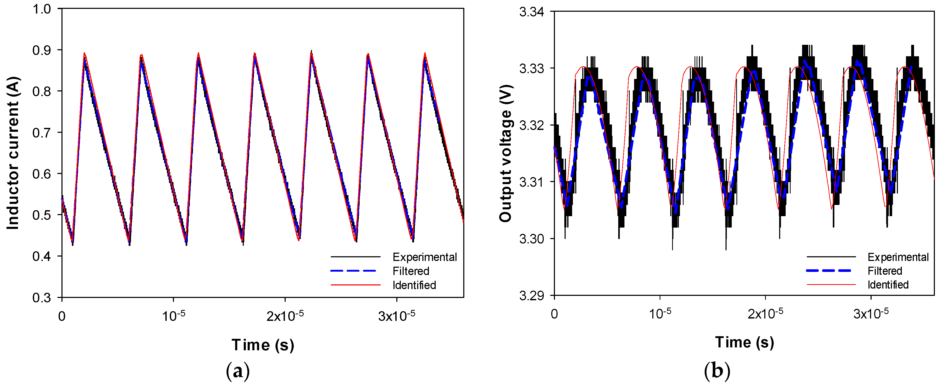
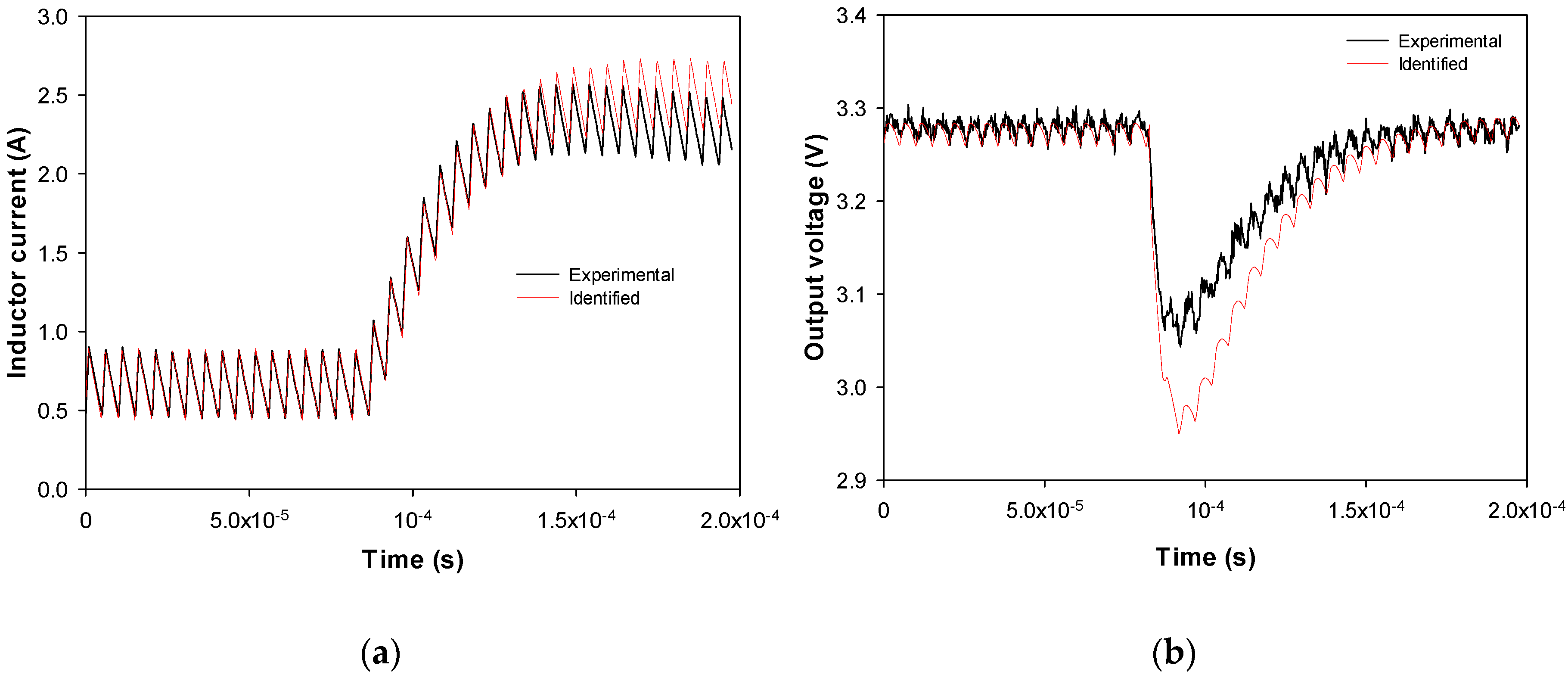
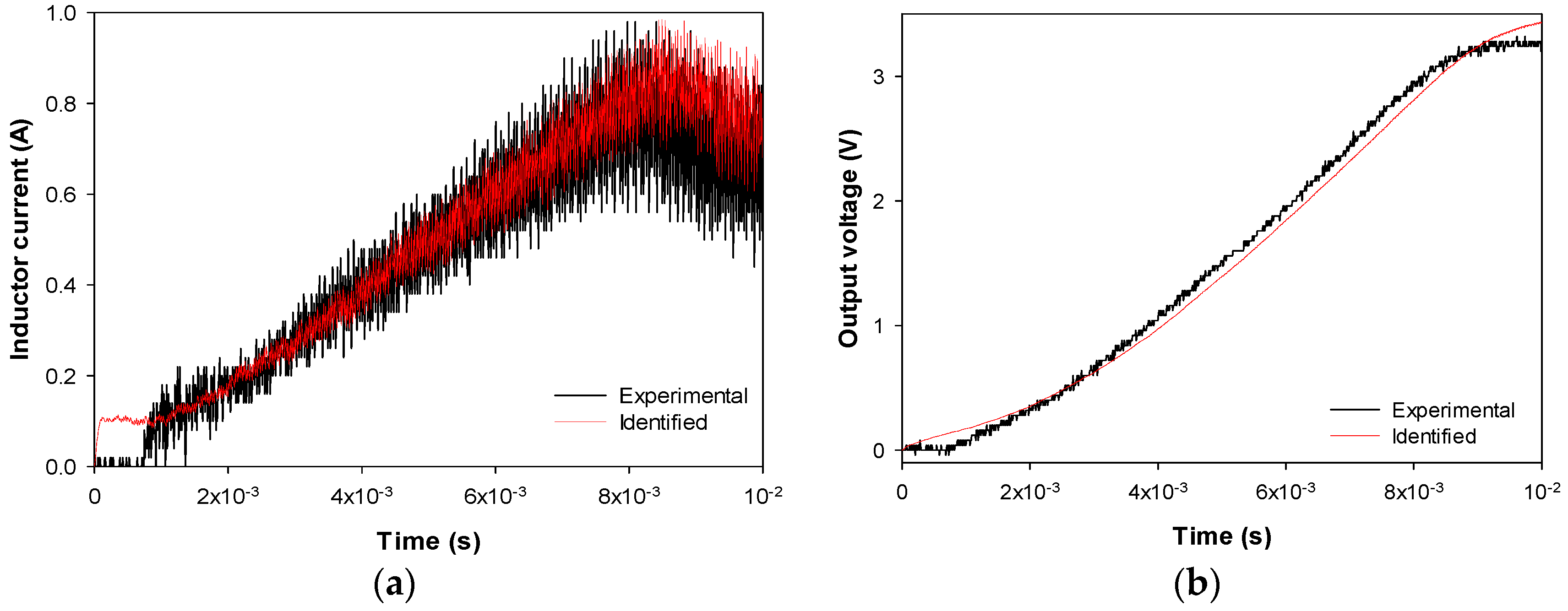
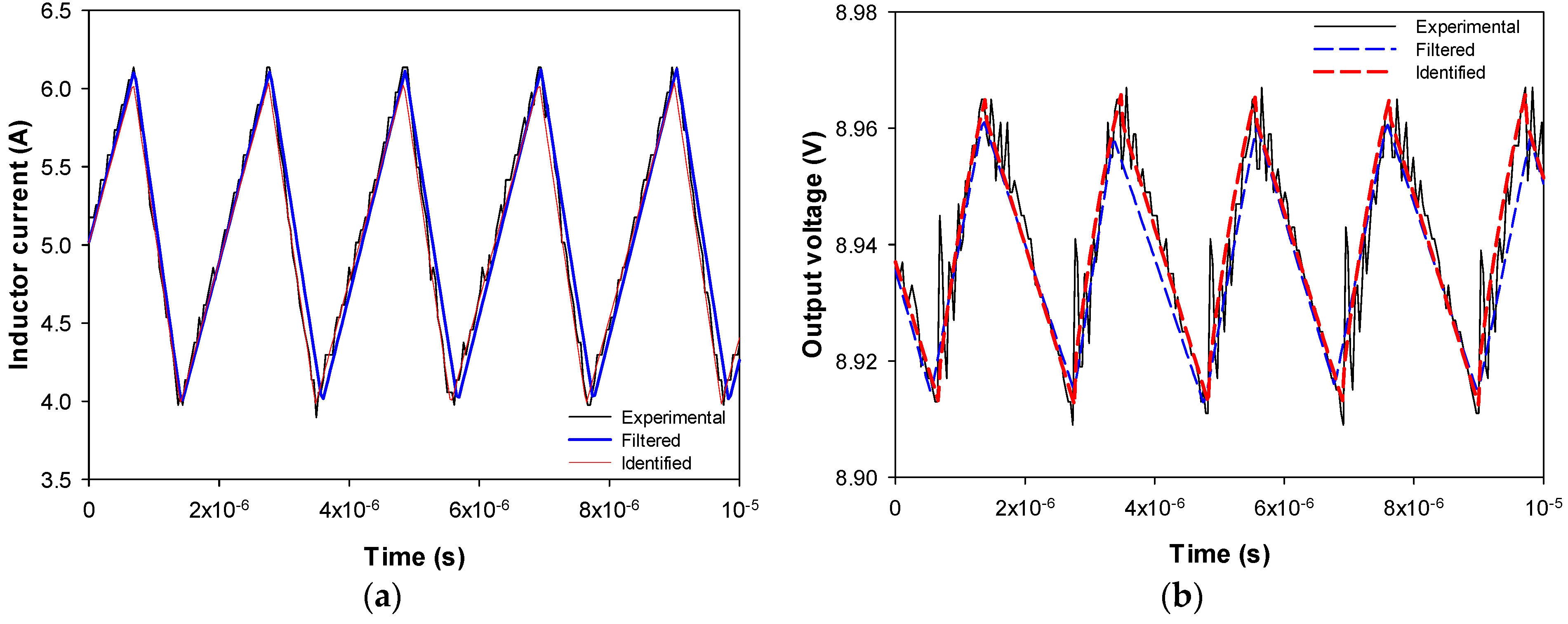
3.1. Experimental Results: Buck Converter Parameter Identification

First, the L, RL, RS, C and RC parameters are identified from the IL, Vin, Iout, and Vout signals acquired under steady state operation with the oscilloscope and current and voltage probes detailed in Section 3.
Results summarized in Table 1 compare the actual parameter values of the TPS40200EVM-002 non-synchronous buck converter and the identified ones, which were obtained by applying the approach detailed in Section 2.1 based on the analysis of the steady state and transient signals of the converter.
The identified value of RLoad was calculated at every time step during steady state as the mean value of the vector obtained by dividing the instantaneous output voltage by the instantaneous output current. Results summarized in Table 1 prove that the parameters of the converter were correctly identified from experimental data, since estimated and actual values are very similar.
Signals IL, Vin, Iout, and Vout were measured during steady state operation and during a load change by means of a 4-channel oscilloscope. Whereas the experimental signals IL and Vout are shown in Figure 7a,b, Vin and Iout are not shown because Vin is almost a constant flat line and Iout is proportional to Vout as a resistive load was used during the experiments. The transient state represented by a sudden load change was applied by a fast connection of a 2 Ω resistor in parallel with the RLoad = 5 Ω load. The switching frequency was set to 200 kHz.
Next, parameters in Table 1 are introduced in the PSIM model in order to compare simulation results attained with the values of the identified parameters against experimental signals. These results are presented in Figure 7 and Figure 8, which show an outstanding match between experimental and simulation results. As observed, experimental signals are noisy, so it is important to filter the experimental signals before the parameter identification stage.
To further validate the approach proposed in this paper, Figure 9a,b show the inductor current and the output voltage of the buck converter during start up. They compare experimental data against the results provided by the simulation model considering the identified values L, RL, RS, C, RC, and the coefficients ai and bi.
Results from Figure 9a,b show a good match between experimental data and simulated results, thus validating the approach proposed in this paper.

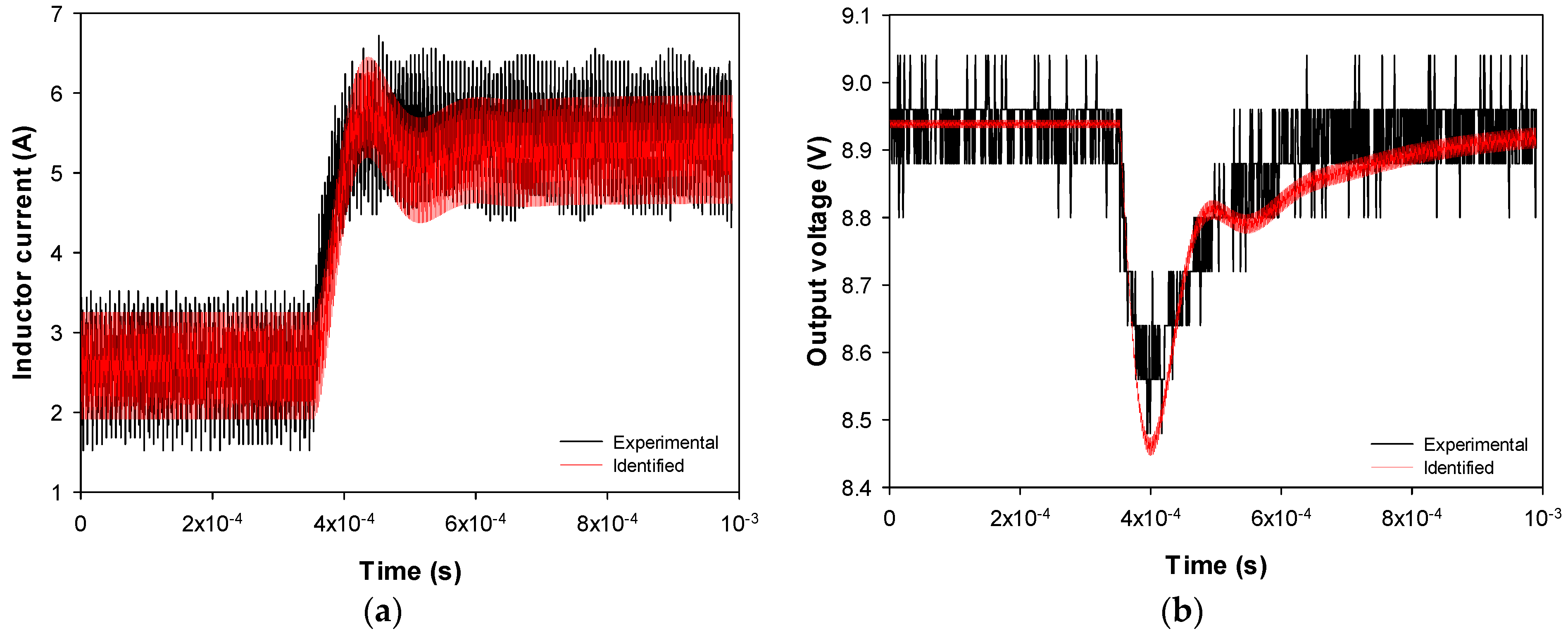
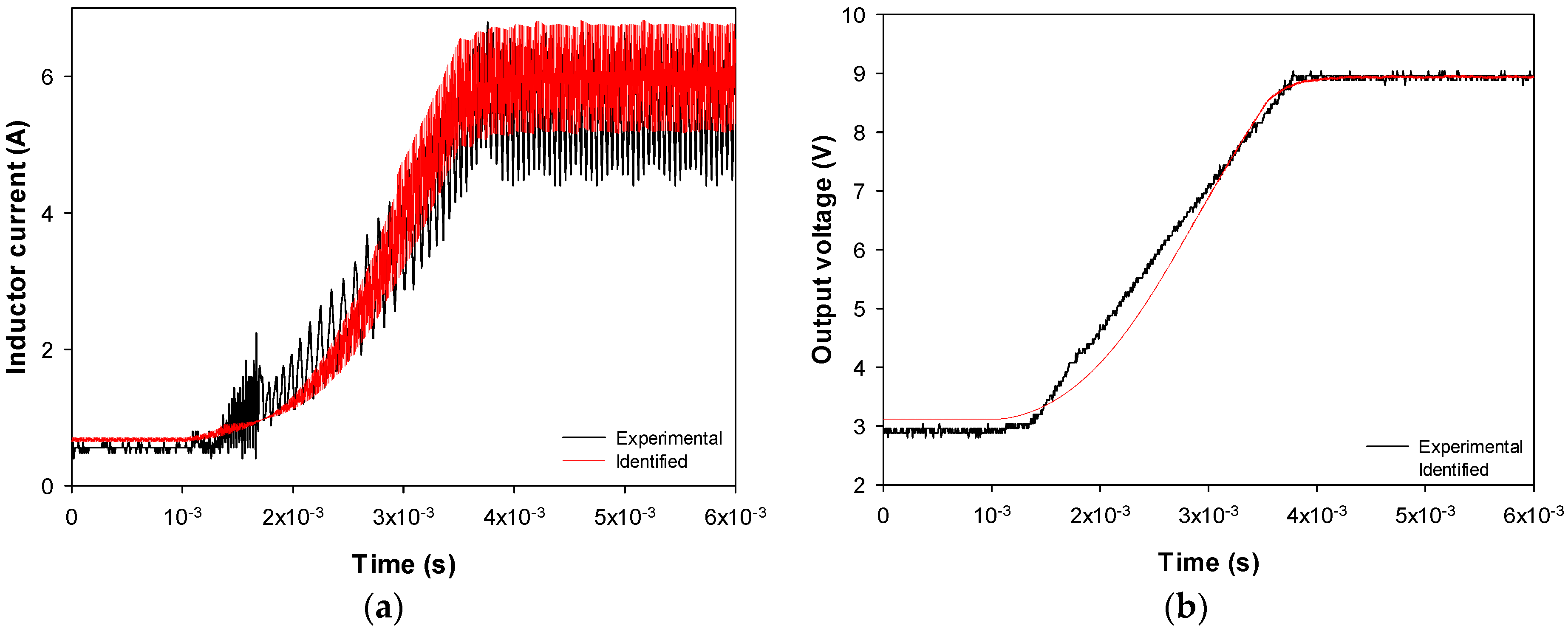
3.2. Experimental Results: Boost Converter Parameter Identification

First, the L, RL, RS1, RS2, C and RC parameters are identified from the IL, Vin, Iout, and Vout signals acquired under steady state operation with the oscilloscope and current and voltage probes detailed in Section 3. Results summarized in Table 2 compare the actual parameter values of the TPS40200EVM-002 synchronous boost converter and the identified ones, which were obtained by applying the approach detailed in Section 2.2 based on the analysis of the steady state and transient responses of converter.
Results summarized in Table 2 prove that the parameters of the boost converter were correctly identified from experimental data, since estimated and actual values are very similar.
Signals IL, Vin, Iout, and Vout were measured during steady state operation and during a load change by means of a 4-channel oscilloscope. Signals IL, Vin, Iout, and Vout were measured during steady state operation and during a load change by means of a 4-channel oscilloscope. Whereas the experimental signals IL and Vout are shown in Figure 10a,b, respectively, Vin and Iout are not shown because Vin is almost a constant flat line and Iout is proportional to Vout, as a resistive load was used during the experiments. A load resistance of 5 Ω was used in open loop conditions, i.e., when dealing with steady state data. Instead, a load resistance of 10 Ω was applied during transient conditions, whereas the resistance connected in parallel with this one, to force the load change was also of 10 Ω. The switching frequency of this converter was 480 kHz.
Next, parameters in Table 2 are introduced in the PSIM model in order to compare simulation results attained with the values of the identified parameters against experimental signals. These results are summarized in Figure 10 and Figure 11, which show an outstanding match between experimental and simulation results.
As observed in the results presented in Figure 10, Figure 11 and Figure 12, experimental signals are noisy, so it is important to filter the experimental signals before the parameter identification stage.
To further validate the approach proposed in this paper, Figure 12a,b show the inductor current and the output voltage of the boost converter during start up. They compare experimental data against the results provided by the simulation model considering the identified values L, RL, RS1, RS2, C, RC, and the coefficients ai and bi.
Results from Figure 12a,b show a good match between experimental and simulated results, thus validating the approach proposed in this paper.

4. Conclusions

Electronic power converters play a key role in many applications involving leading industry sectors such as naval, aerospace or automotive, among others. Parameter identification is a discipline focused on determining the parameters of the model of a system to replicate its dynamic behavior from experimental data. However, it is a challenging task due to the complexity of real systems, and the wide range of working conditions. This paper has presented a parameter identification approach for electronic buck and boost DC-DC converters based on white-box models. The parameters have been identified based on experimental data collected under both steady-state and transient operating conditions. Experimental and simulation results based on the white-box models with the identified values of the parameters show the feasibility and accuracy of the proposed approach. It is worth noting that this approach can be also applied to other electronic converters and devices such as passive and active filters.

Author Contributions

Conceptualization, methodology and validation, J.-R.R. and M.M.-E.; experimental data M.M.-E., writing J.-R.R., supervision S.B. and A.G.

Funding

This research was funded by Generalitat de Catalunya, grant number SGR 2017 SGR 967, the Spanish Ministry of Economy and Competitiveness, grant number TRA2016-80472-R and the European Commission through the Clean Sky program, grant number 755332-AEMS-IdFit.

Acknowledgments

The authors are grateful to Gabriel Rojas for his technical support.

Conflicts of Interest

The authors declare no conflict of interest.

References

  1. Nguyen, V.; Huynh, H.; Kim, S.; Song, H.; Nguyen, V.H.; Huynh, H.A.; Kim, S.; Song, H. Active EMI Reduction Using Chaotic Modulation in a Buck Converter with Relaxed Output LC Filter. Electronics 2018, 7, 254. [Google Scholar] [CrossRef]
  2. Ahmeid, M.; Armstrong, M.; Gadoue, S.; Algreer, M.; Missailidis, P.; Al-Greer, M.; Missailidis, P. Real-Time Parameter Estimation of DC–DC Converters Using a Self-Tuned Kalman Filter. IEEE Trans. Power Electron. 2017, 32, 5666–5674. [Google Scholar] [CrossRef] [Green Version]
  3. Zhang, Y.; Li, X.; Sun, C.; He, Z.; Zhang, Y.; Li, X.; Sun, C.; He, Z. Improved Step Load Response of a Dual-Active-Bridge DC–DC Converter. Electronics 2018, 7, 185. [Google Scholar] [CrossRef]
  4. Qian, S.; Ren, L.; Gong, C.; Wang, H. A unified feature parameter extraction strategy based on system identification for the Buck converter with linear or nonlinear loads. In Proceedings of the IECON 2016—42nd Annual Conference of the IEEE Industrial Electronics Society, Florence, Italy, 23–26 October 2016; pp. 388–393. [Google Scholar]
  5. Ye, C.; Feng, S.; Xu, P.; Liu, J. Transmission Line Parameter Identification Considering Non-Synchronized Time of Fault Recording Information. In Proceedings of the 2018 2nd IEEE Advanced Information Management, Communicates, Electronic and Automation Control Conference (IMCEC), Xi’an, China, 25–27 May 2018; pp. 1749–1753. [Google Scholar]
  6. Chen, W.; Gong, Q.; Wang, T.; Yin, C.; Yao, J. A real-parameter genetic algorithm application in parameters identification for synchronous generator. In Proceedings of the 2009 IEEE International Conference on Intelligent Computing and Intelligent Systems, Shanghai, China, 20–22 November 2009; pp. 762–766. [Google Scholar]
  7. Jiya, I.; Gurusinghe, N.; Gouws, R.; Jiya, I.N.; Gurusinghe, N.; Gouws, R. Electrical Circuit Modelling of Double Layer Capacitors for Power Electronics and Energy Storage Applications: A Review. Electronics 2018, 7, 268. [Google Scholar] [CrossRef]
  8. Buiatti, G.M.; Amaral, A.M.R.; Cardoso, A.J.C. ESR Estimation Method for DC/DC Converters Through Simplified Regression Models. In Proceedings of the 2007 IEEE Industry Applications Annual Meeting, New Orleans, LA, USA, 23–27 September 2007; pp. 2289–2294. [Google Scholar]
  9. Oliver, J.A.; Prieto, R.; Romero, V.; Cobos, J.A. Behavioural Modelling of DC-DC Converters for Large-Signal Simulation of Distributed Power Systems. In Proceedings of the Twenty-First Annual IEEE Applied Power Electronics Conference and Exposition, APEC’06, Dallas, TX, USA, 19–23 March 2006; pp. 1204–1209. [Google Scholar]
  10. Algreer, M.M.F.S. Microprocessor Based Signal Processing Techniques for System Identification and Adaptive Control of DC-DC Converters. Ph.D. Thesis, Newcastle University, Newcastle, UK, 2012. [Google Scholar]
  11. Munster, D. Parameter Identification: A Comparison of Methods. 2009, pp. 4–7. Available online: http://www.math.vt.edu/ugresearch/munster_drayton.pdf (accessed on 28 September 2018).
  12. Nelles, O. Nonlinear System Identification. From Classical Approaches to Neural Networks and Fuzzy Models; Springer: Berlin/Heidelberg, Germany, 2001. [Google Scholar]
  13. Petrone, R.; Zheng, Z.; Hissel, D.; Péra, M.C.; Pianese, C.; Sorrentino, M.; Becherif, M.; Yousfi-Steiner, N. A review on model-based diagnosis methodologies for PEMFCs. Int. J. Hydrog. Energy 2013, 38, 7077–7091. [Google Scholar] [CrossRef]
  14. Valdivia, V. Behavioral Modeling and Identification of Power Electronics Converters and Subsystems Based on Transient Response. Ph.D. Thesis, Universidad Carlos III de Madrid, Madrid, Spain, 2013. [Google Scholar]
  15. Wehbe, Y.; Fan, L.; Miao, Z. Least squares based estimation of synchronous generator states and parameters with phasor measurement units. In Proceedings of the North American Power Symposium (NAPS 2012), Champaign, IL, USA, 9–11 September 2012. [Google Scholar]
  16. Gietler, H.; Unterrieder, C.; Berger, A.; Priewasser, R.; Lunglmayr, M. Low-complexity, high frequency parametric system identification method for switched-mode power converters. In Proceedings of the 2017 IEEE Applied Power Electronics Conference and Exposition (APEC), Tampa, FL, USA, 26–30 March 2017; pp. 2004–2009. [Google Scholar]
  17. Linares-Flores, J.; Hernandez Mendez, A.; Garcia-Rodriguez, C.; Sira-Ramirez, H. Robust Nonlinear Adaptive Control of a “Boost” Converter via Algebraic Parameter Identification. IEEE Trans. Ind. Electron. 2014, 61, 4105–4114. [Google Scholar] [CrossRef]
  18. Chen, C.; Li, L.; Zhang, Q.; Tong, Q.; Liu, K.; Lyu, D.; Min, R. Online Inductor Parameters Identification by Small-Signal Injection for Sensorless Predictive Current Controlled Boost Converter. IEEE Trans. Ind. Inform. 2017, 13, 1554–1564. [Google Scholar] [CrossRef] [Green Version]
  19. Xu, J.; Armstrong, M.; Al-Greer, M. Parameter Estimation of DC-DC Converters Using Recursive Algorithms with Adjustable Iteration Frequency. In Proceedings of the 2018 IEEE 19th Workshop on Control and Modeling for Power Electronics (COMPEL), Padua, Italy, 25–28 June 2018; pp. 1–8. [Google Scholar]
  20. Ren, L.; Gong, C. Modified hybrid model of boost converters for parameter identification of passive components. IET Power Electron. 2018, 11, 764–771. [Google Scholar] [CrossRef]
  21. Buiatti, G.M.; Amaral, A.M.R.; Cardoso, A.J.M. An unified method for estimating the parameters of non-isolated DC/DC converters using continuous time models. In Proceedings of the 29th International Telecommunications Energy Conference (INTELEC 2007), Rome, Italy, 30 September–4 October 2007; pp. 334–341. [Google Scholar]
  22. Texas Instruments. Using the TPS40200. User’s Guide; Texas Instruments: Dallas, TX, USA, 2009. [Google Scholar]
  23. Texas Instruments. Demystifying Type II and Type III Compensators Using OpAmp and OTA for DC/DC Converters. Application Report; Texas Instruments: Dallas, TX, USA, 2014. [Google Scholar]
  24. Texas Instruments. TPS61089-PWR742 Evaluation Module. User’s Guide; Texas Instruments: Dallas, TX, USA, 2016. [Google Scholar]
Figure 1. (a) Buck converter including the control loop. (b) Detail of the controller included in the commercial TPS40200EVM-002 non-synchronous DC-DC buck converter from Texas Instruments [22]. (c) Equivalent circuit during TON. (d) Equivalent circuit during TOFF.
Electronics 07 00393 g001
Figure 2. Output voltage of the buck converter during a sudden load change. Parameter sweep of RC2 (a) and C2 (b) performed in PSIM to identify the values of these parameters.
Electronics 07 00393 g002
Figure 3. Buck converter. Flowchart of the identification approach proposed in this work based on the acquisition of experimental signals during steady state and transient operating conditions.
Electronics 07 00393 g003
Figure 4. (a) Boost converter including the control loop. (b) Detail of the controller included in the commercial TPS61089EVM-742 synchronous DC-DC boost converter from TI, which is based on an operational transconductance amplifier (OTA), where gm = 190 µS [24]. (c) Equivalent circuit during TON. (d) Equivalent circuit during TOFF.
Electronics 07 00393 g004
Figure 5. Boost converter. Flowchart of the identification approach proposed in this work based on the acquisition of experimental signals during steady state and transient operating conditions.
Electronics 07 00393 g005
Figure 6. Experimental setup including the TPS40200EVM-002 non-synchronous buck converter and the TPS61089EVM-742 synchronous boost converter, the load, the oscilloscope, power supply and the voltage and current probes.
Electronics 07 00393 g006
Figure 7. Buck converter. Steady state experimental data. (a) Inductor current. (b) Output voltage.
Electronics 07 00393 g007
Figure 8. Buck converter. Experimental results attained when applying a sudden load change against simulation results obtained from PSIM simulations performed with the values of the identified parameters L, RL, RS, C, RC, and the coefficients ai and bi. (a) Inductor current. (b) Output voltage.
Electronics 07 00393 g008
Figure 9. Buck converter. Experimental results attained during startup against simulation results obtained from PSIM simulations performed with the values of the identified parameters L, RL, RS, C, RC, and the coefficients ai and bi. (a) Inductor current. (b) Output voltage.
Electronics 07 00393 g009
Figure 10. Boost converter. Steady state experimental data. (a) Inductor current. (b) Output voltage.
Electronics 07 00393 g010
Figure 11. Boost converter. Experimental results attained when applying a sudden load change against simulation results obtained from PSIM simulations performed with the values of the identified parameters L, RL, RS1, RS2, C, RC, and the coefficients ai and bi. (a) Inductor current. (b) Output voltage.
Electronics 07 00393 g011
Figure 12. Boost converter. Experimental results attained during startup against simulation results obtained from PSIM simulations performed with the values of the identified parameters L, RL, RS1, RS2, C, RC, and the coefficients ai and bi. (a) Inductor current. (b) Output voltage.
Electronics 07 00393 g012
Table 1. Comparison of actual and identified buck converter parameters.
ParameterVariableActual (Datasheet)Identified
InductanceL33 μH35.2 μH
Inductor resistanceRL60 mΩ55.8 mΩ
Switch S1RS<105 mΩ39.1 mΩ
Capacitance (smaller capacitor)C120 μF16.8 μF
ESR of output capacitor (smaller)Rc165 mΩ60.9 mΩ
Capacitance (larger capacitor)C2440 μF490 μF
ESR of output capacitor (larger)Rc2300 mΩ280 mΩ
Equivalent ESR (large and small capacitors)Rc,eq56.4 mΩ54.5 mΩ
Equivalent capacitance (large and small capacitors)Ceq29.92 μF25.4 μF
a00−0.010
a14.73 × 10−41.38 × 10⁻³
a21.55 × 10−94.18 × 10⁻⁹
Transfer function coefficients of the controllerbo1.01
b14.70 × 10-47.10 × 10⁻⁴
b201.42 × 10−12
Load resistanceRLoad5 Ω4.997 Ω
Table 2. Comparison of actual and identified boost converter parameters.
ParameterVariableActual (Datasheet)Identified
InductanceL1.8 μH1.9 μH
Inductor resistanceRL12.6 mΩ7.5 mΩ
Equivalent ESR (large and small capacitors)Rc,eq0.65 mΩ1.06 mΩ
Equivalent capacitance (large and small capacitors)Ceq67.0 μF47.9 μF
Switch S1RS1<31 mΩ10.92 mΩ
Switch S2RS2<44 mΩ16.38 mΩ
a00.00.1
a14.7 × 10−95.0 × 10⁻⁴
Transfer function coefficients of the controllerbo1.01.0
b18.18 × 10−56.36 × 10⁻⁵
Load resistanceRLoad5 Ω4.969 Ω

