Abstract
This paper presents a novel bidirectional double uneven power (BiDUP) based dc-dc converter and its design and control methods. The proposed converter utilizes two dual active bridge (DAB) converters with different power ratings in a special way to realize zero current switching (ZCS), where both turn-on and turn-off switchings occur under the zero-current condition. A design example of the proposed BiDUP converter is presented for medium voltage (MV) and high-power solid-state transformer (SST) systems where both voltage transformation and bidirectional power flow are required. The main features of the proposed converter are to reduce both the switching losses in power semiconductor devices and the filter inductance requirement simultaneously. To verify the feasibility of the proposed converter, a simulation study on the BiDUP converter based SST in a distribution system is presented. Furthermore, to validate the operational principle of the proposed converter, an experimental study using a small-scale prototype is also presented.
1. Introduction
The solid-state transformer (SST) (also known as a power electronic transformer) has recently gained much attention and been extensively investigated for its potential applications from simply replacing traditional low-frequency (50 or 60 Hz) transformers in distribution systems to integrate renewable energy sources [1,2,3] or energy storage, in order to interface locomotive traction systems [4,5]. Basically, the SST utilizes a medium- to high-frequency (several kHz to tens of kHz) transformer to achieve voltage transformation and galvanic isolation. Hence, the volume and weight of the SST is much smaller than that of a low-frequency traditional transformer and, in turn, the overall efficiency and power density of the system can be improved significantly. Moreover, the SST is known to have additional functionalities which are not available with a tradition transformer: reactive power compensation, active filtering, fault ride-through, and so forth [1,2,3,4,5].
Numerous circuit configurations of the SST have already been developed and introduced in the literature: ac-ac (single-stage) [6,7], ac-dc-ac (two-stage) [8,9,10], and ac-dc-dc-ac (three-stage) [3,4,5,11,12]. However, most of the SSTs developed so far for field applications have adopted the ac-dc-dc-ac three-stage configuration [12], because matured technologies for each power conversion stage are already available and many attractive features, such as reactive power compensation, voltage sag compensation, and renewable energy integration, might be achieved [13]. Figure 1a shows the functional concept of the ac-dc-dc-ac SST system. The SST typically consists of a medium-voltage (MV, tens of kV) ac-dc active rectifier, an isolated high-frequency dc-dc converter, and a low-voltage dc-ac inverter. For MV and high-power applications, the modular approach, where modular cells are connected in series and/or in parallel, can be employed as shown in Figure 1b.
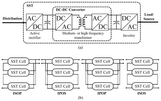
Figure 1.
(a) The functional concept of an ac-dc-dc-ac three-stage solid-state transformer (SST) system and (b) various modular configurations of a SST system (ISOP: input-series output-parallel, IPOS: input-parallel output-series, IPOP: input-parallel output-parallel, ISOS: input-series output-series).
Although many matured technologies and topologies for the MV active rectifier and the low-voltage inverter have been developed and are already in use, only a few dc-dc converter topologies suitable for the SST application are available. Since the dc-dc converter in the SST system operates with a high frequency, the switching loss of the high-frequency transformer and the power devices should be restricted. Furthermore, the bidirectional power flow capability should be available. In the literature, a dual active bridge (DAB) dc-dc converter with phase-shift control has been introduced as the most attractive candidate for high-power applications requiring isolation, low switching loss, and bidirectional power flow [3]. However, the DAB dc-dc converter operates with the zero voltage switching (ZVS) mode only under the limited range of load conditions and suffers from additional conduction losses due to the high circulating current at heavy load. Therefore, high efficiency is quite limited to a certain load range with the DAB dc-dc converter [12].
The DAB dc-dc converter for high-power applications has another problem that a large amount of filter inductance is required to maintain the continuous conduction mode (CCM). It is in practice difficult to manufacture an inductor with large inductance at high-power levels. If the operation mode is restricted to the discontinuous conduction mode (DCM), the required filter inductance can be reduced significantly. The DCM implies increased peak current values, but the magnitude of the current peaks is readily tolerated by modern switching devices. Furthermore, since the average current does not increase in the DCM, the same switching devices as in the CCM might be used [14]. However, the turn-off switching loss will increase since the switching devices turn off at the increased current peaks in the DCM converter. Therefore, reducing not only power losses in the switching devices but also required filter inductance is critical in realizing a practical high-power dc-dc converter. Several authors have attempted to address these issues with resonant switching or soft switching [15] to reduce losses [16]. In [17], a double uneven power (DUP) converter was firstly introduced to reduce the power losses and output filter inductance in a high-power dc-dc converter. However, the DUP converter was designed for renewable energy applications where the unidirectional power flow was adequate.
In this paper, a novel bidirectional double uneven power (BiDUP) converter based dc-dc converter and its design and control methods will be introduced. The proposed converter utilizes two DAB converters with different power ratings in a special way to realize zero current switching (ZCS), where both turn-on and turn-off switchings occur under the zero-current condition. The proposed BiDUP converter is designed for MV and high-power SST systems where both voltage transformation and bidirectional power flow are required. The main objectives of the proposed converter are (1) to reduce the switching losses in power semiconductor devices and (2) to reduce the filter inductance requirement. A simulation study on the BiDUP converter-based SST in a distribution system will be performed to verify the feasibility of the proposed converter. Furthermore, an experimental study using a small-scale prototype will be presented to validate the operational principle of the proposed converter.
2. Bidirectional Double Uneven Power (BiDUP) Converter
2.1. Circuit Configuration
The structure of the proposed BiDUP converter has two DAB converters (‘main’ and ‘control’) with different power ratings as shown in Figure 2. A basic idea of the proposed converter is that the ‘main’ converter processes majority of the overall power (e.g., 80–90%) under ZCS condition, meanwhile the ‘control’ converter delivers a small share of power (e.g., 10–20%) under hard-switching (HS) condition. The ‘main’ and ‘control’ converters are connected in parallel at the input side and in series at the output side. The voltage ratings of the switching devices, such as IGBTs (Insulated Gate Bipolar Transistors) or MOSFETs (Metal-Oxide-Semiconductor Field-Effect Transistors), at the input side are the same for both the converters since they are connected in parallel. However, the switching devices of the ‘main’ converter require much larger current ratings than that of the ‘control’ converter since the ‘main’ converter processes much larger power. Due to the series connection, the current ratings of the switching devices at the output side are the same for both the converter, but the ‘main’ converter requires larger voltage ratings.
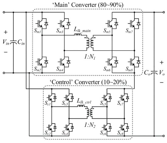
Figure 2.
The proposed bidirectional double uneven power (BiDUP) dc-dc converter.
The transformer turn-ratio of the ‘main’ converter, N1, should be designed to be bigger than that of the ‘control’ converter, N2, so that the ‘main’ converter performs the majority of the required voltage transformation. Meanwhile, N2 is generally designed to be a much smaller value, so that the ‘control’ converter can provide the voltage which is just enough to control the overall delivering power of the system in a required range. In this way, the overall power can be controlled with a small amount of the input current in the ‘control’ converter. To minimize the required filter inductance, N1 and N2 should be designed following a special relationship which makes the output current take an isosceles triangle shape. The detailed design method will be presented in <Section 2.4>.
2.2. Fundamental Operation
Although the proposed BiDUP converter consists of two DAB converters, which normally use phase-shift control in both the input and output active bridges simultaneously, its switching strategy is based on simple hard-switching duty-cycle control. As the name of the converter implies, the BiDUP converter has the bidirectional power flow capability: forward, i.e., from the primary (higher voltage) side to the secondary (lower voltage) side), and backward (from the secondary side to the primary voltage side.) During the forward operation, all the switches in the active bridges in the secondary side are turned off so that they simply form full-bridge diode rectifiers connected in series in the output. On the other hand, during the backward operation, all the switches in the primary side are turned off so that they form diode rectifiers connected in parallel in the input. Figure 3 shows the switching signals for the ‘main’ and ‘control’ converters and the typical current waveforms for both the forward and backward operations. The figure also shows the switching states and the current conduction paths.
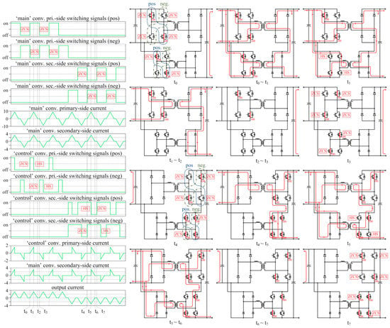
Figure 3.
Typical waveforms and current conduction paths according to the switching states.
2.2.1. Forward Operation
The ‘main’ converter regulates the primary voltage (Vin) to the voltage level close to, but less than, the secondary voltage (Vo) and operates with the maximum duty-ratio (0.5) all the time to keep this value as constant as possible for a whole switching period. Therefore, the ‘main’ converter does not require any complicated control because it operates with the fixed duty-ratio at a fixed switching frequency. Meanwhile, the ‘control’ converter adjusts the overall power flow by varying its turn-on duty-ratio (Don). For the ‘control’ converter, either duty-cycle control (hard-switching) or phase-shift control (soft-switching) might be used. However, the soft-switching can be achieved only in the lagging leg of the active bridge under the DCM condition. Moreover, the soft-switching would increase the conduction losses. Hence, the duty-cycle control is adopted in this paper.
- (1)
- t0: t0 is the instant when a new switching period starts by turning off the negative switch pair in the ‘main’ converter and turning on the positive switch pairs in both the ‘main’ and ‘control’ converters simultaneously. Since there was no current flowing in both the converters prior to t0, not only the negative switch pair in the ‘main’ converter is turned off under ZCS condition, but also the positive switch pairs are turned on under ZCS condition as indicated in Figure 3.
- (2)
- t0–t1: during this interval, the sum of the output voltages of both the converters (N1·Vin + N2·Vin) is larger than the terminal output voltage (Vo), so that the transformer currents in both the converters and the output current increase linearly. The rate of the output current change (dio/dt) is determined by the filter inductance (including the leakage inductances of the transformers) and the transformer turn-ratios.
- (3)
- t1: t1 is the instant when the positive switch pair in the ‘control’ converter is turned off under HS condition. Therefore, the turn-off switching loss is inevitable in the switch pair. However, since the power processed by the ‘control’ converter itself is only a small portion of the overall power, the turn-off switching loss in the ‘control’ converter is not significant. As can be seen from the figure, there is a regenerative current flowing through the antiparallel diodes of the negative switch pair in the ‘control’ converter for a short time period right after turning off the positive switch pair. This current is due to the leakage inductance of the transformer in the ‘control’ converter.
- (4)
- t1–t2: after the regenerative current vanishes, there is no current flowing in the transformer of the ‘control’ converter. The output current is now flowing directly through both the legs of the diode bridge in the ‘control’ converter, producing zero output voltage. Since the output voltage of the ‘main’ converter alone (N1·Vin) is smaller than the terminal output voltage (Vo), the output current and the current in the ‘main’ converter decease linearly during this interval and reaches zero before the next half switching period starts at t3. Again, the rate of the output current change (dio/dt) is determined by the filter inductance and the transformer turn-ratios and, in turn, the shape of the output current waveform can be manipulated by them. The detailed design method shaping the output current will be presented in the next section.
- (5)
- t2–t3: during this interval, even though the positive switch pair in the ‘main’ converter still remains turned on, there is no current flowing in both the ‘main’ and ‘control’ converters. The total output current from the converters is zero and the load current is supplied by the output filter capacitor (Co).
- (6)
- t3: t3 is the instant when a new half switching period starts by turning off the positive switch pair in the ‘main’ converter and turning on the negative switch pairs in both the converters. Since there was no current flowing in both the converters prior to t3, the ZCS is achieved. The rest of the switching period is symmetrical to the previous half switching period as explained and will not be elaborated upon here.
2.2.2. Backward Operation
To reverse the direction of the current, all the switches of the active bridges in the primary sides are turned off to form two diode bridges connected in parallel. However, the active bridge in the secondary side of the ‘main’ converter now starts switching with the fixed duty-ratio (0.5) at a fixed switching frequency. Meanwhile, the ‘control’ converter controls the overall power flow by varying its shoot-through duty-ratio (Dsh).
- (1)
- t4: t4 is the instant when a new switching period starts by turning off the positive switch pair in the ‘main’ converter and turning on the negative switch pairs in both the ‘main’ and ‘control’ converters simultaneously. Since there was no current flowing in both the converters prior to t4, all the switch pairs change their switching-states under ZCS condition as indicated in Figure 3. Since the positive switch pair in the ‘control’ converter was already turned on prior to t4, now, all the switches in the ‘control’ converter are turned on to form a shoot-through path.
- (2)
- t4–t5: during this interval, the sum of the secondary side voltages of both the converters (N1·Vin + 0 = N1·Vin) is smaller than the terminal output voltage (Vo), so that the current in the filter inductor, assumed to be placed separately at the output, decreases linearly. Since the rate of the secondary current change (dio/dt) is, again, determined by the filter inductance and the transformer turn-ratios, it is the same as that in the forward operation.
- (3)
- t5: t5 is the instant when the positive switch pair in the ‘control’ converter is turned off under HS condition. Again, the turn-off switching loss is not significant because only a small share of power is processed by the ‘control’ converter. As can be seen from the current conduction path, the output current is now forced to start flowing in the ‘control’ converter’s transformer. If the leakage inductance of the ‘control’ converter’s transformer is large enough to prevent the rapid increase of the transformer current and to cause intolerable voltage surges, an additional snubbing or clamping circuit might be required.
- (4)
- t5–t6: now, the output current is flowing through the transformers in both the converters, so that the sum of the secondary voltages of both the converters (N1·Vin + N2·Vin) is larger than the terminal secondary voltage (Vo). Consequently, the secondary current increases linearly back to zero before the next half switching period starts at t7.
- (5)
- t6–t7: this is the non-conducting period in the DCM. Although all the switches are maintaining their switching-states, there is no current flowing in any of the converters. The load current is supplied by the input filter capacitor (Cin).
- (6)
- t7: t7 is the instant when a new half switching period starts by turning off the negative switch pair in the ‘main’ converter and turning on the positive switch pairs in both the converters. Since there was no current flowing in both the converters prior to t7, the ZCS is achieved. The rest of the switching period is symmetrical to the previous half switching period as explained and will not be elaborated upon here.
2.3. Equivalent Circuits
To facilitate the understanding of the operational principle of the proposed BiDUP converter, equivalent circuits can be utilized. By summarizing the fundamental operations of the converter in the previous subsection, two equivalent circuits for the forward and backward operations can be devised separately as shown in Figure 4. Since the ‘main’ converter always operates with the full duty ratio (0.5), keeping a constant voltage ratio (N1·Vin) from the primary side to the secondary side, it can be modelled as a single voltage source connected to the secondary terminal voltage in series through filter inductance with opposite polarity.
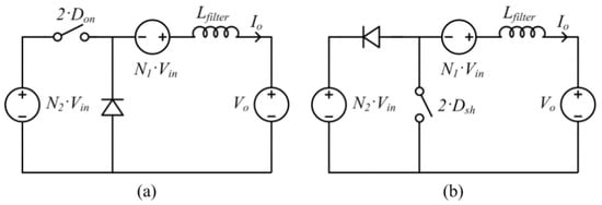
Figure 4.
Equivalent circuits of the BiDUP converter for the (a) forward and (b) backward operations.
In the forward operation case, the ‘control’ converter can be modelled with a single switch, a single diode, and a voltage source (N2·Vin) as shown in Figure 4a. Owning to the nature of the full wave rectification, the equivalent circuit of the ‘control’ converter produces the output voltage of (2·Don)(N2·Vin), where Don is the turn-on duty ratio of the ‘control’ converter. The overall equivalent circuit for the forward operation has exactly the same circuit configuration as a buck converter operating in the DCM. Therefore, the average current in the filter inductor, in turn, the average delivering power can be controlled by varying Don.
The equivalent circuit for the backward operation is very similar with the forward one except for the location of the single switch and the single diode. Their locations are swapped and the switch is now controlled with the shoot-through duty-ratio (2·Dsh). The overall equivalent circuit for the backward operation has exactly the same circuit configuration as a boost converter operating in the DCM. Therefore, the average current in the filter inductor can be controlled by varying Dsh.
2.4. Main Design Parameters (N1, N2, and Lfilter)
The medium- or high-frequency transformers of both the ‘main’ and ‘control’ converters are represented with ideal transformers and leakage inductors (Llk_main and Llk_ctrl, respectively) referenced to the primary side of the transformers in Figure 2. In the case of the ‘main’ converter, no regenerative current, which might have increased the magnitudes of the input and output current ripples, is caused by the leakage inductance (Llk_main) because the converter switches under ZCS condition. The leakage inductance only acts as a current limiting filter. Hence, the transformer of the ‘main’ converter can be designed to have large leakage inductance so that the required filter inductance (Lfilter) can be obtained. From the power density point of view, integrating the filter inductor into the leakage inductor is highly recommended [18]. Furthermore, allowing large leakage inductance facilitates manufacturing of transformers especially with high-voltage isolating requirements. On the other hand, the leakage inductor in ‘control’ converter (Llk_ctrl) not only generates regenerative currents due to the hard switching, but also causes imbalance in the total filter inductance depending on the switching states. Therefore, the leakage inductance of the ‘control’ converter should be designed to be as small as possible.
To minimize the required filter inductance, the output current waveform should have an isosceles triangle shape. The isosceles triangle waveform under the DCM results in the least amount of the required filter inductance at a given peak output current rating. To realize this, the ‘main’ and ‘control’ converters have to work together and the transformer turn-ratios should be designed following a special relationship. Assuming that the required filter inductor (Lfilter) is placed separately at the output and considering only the forward power flow, the isosceles triangle waveform means that the rise time and the fall time of the output current are always kept the same. During the current rise time, both the converters work together to magnetizing the filter inductor. Since the outputs are connected in series, the impressed voltage to the filter inductor can be expressed as below:
During the current fall time, all the switches in the ‘control’ converter are turned off, so that only the output voltage from the ‘main’ converter is applied to the filter inductor. Hence, the demagnetizing voltage can be expressed as below:
If the magnitudes of Vmag and Vdemag are the same while their polarities are opposite, the rise time and the fall time of the output current can be kept identical. By equating the absolute values of (1) and (2), the following relationship can be achieved:
Therefore, if the transformer turn-ratios are designed following the above relationship, the isosceles triangle shaped output current can be ensured. For example of 1-to-1 voltage transformation where the input and output voltages are the same (Vin = Vo), N1 and N2 can theoretically have any pair of values on the line of Figure 5a. However, N2 is generally designed to be much smaller than N1, so that the majority of power can be processed by the ‘main’ converter under the ZCS condition.
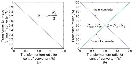
Figure 5.
(a) Design example of the transformer turn-ratios (N1 and N2) and (b) its power distribution between the ‘main’ and ‘control’ converters depending on N2, when the input and output voltages are assumed to be the same.
The power distribution between the ‘main’ and ‘control’ converters can also be expressed in terms of N1 and N2. When magnetizing the filter inductor, the output currents of the ‘main’ and ‘control’ converters are the same as the total output current (io) since they are connected in series. Therefore, the primary-side currents of the ‘main’ and ‘control’ converters (imain_p and ictrl_p) can be expressed as below, respectively.
When demagnetizing the filter inductor, the secondary-side current of the ‘control’ converter becomes 0 instantly, but the secondary-side current of the ‘main’ converter still flows until the output current reaches 0. Therefore, instantaneous currents in the primary sides during this period can be expressed as below:
From (4) and (5), the average currents of the primary sides of both the converters (Imain_p and Ictrl_p) for one switching period can be expressed as:
Since the average input voltage is the same for both the converters, the average power distribution ratio between the converters can be expressed as below:
For the same example above, the power distribution between the ‘main’ and ‘control’ converters can be expressed as shown in Figure 5b.
It is worth noting that N2 should be designed depending on applications, and the input and output voltage conditions. The larger the variations in both the input and output voltages from their nominal values, the bigger N2 should be to ensure the robust operation. However, if N2 is increased, then more power will be processed by the ‘control’ converter and, in turn, the efficiency of the overall system can be lowered. Therefore, a system designer should decide N2 by taking into account the trade-off between the robustness and the efficiency.
The output filter inductance (Lfilter) can, now, be designed to limit the maximum peak value of the output current at the rated power. Since the output current is kept to have an isosceles triangular shape obeying (3), the maximum duty ratio that the ‘control’ converter can have is 0.25 and this is also the boundary condition of the DCM. Therefore, the required filter inductance can be easily achieved using the following equation:
where ipeak is the maximum peak current at the rated power. In this way, the required filter inductance can be significantly reduced compared with that of conventional dc-dc converters. Furthermore, it is worth mentioning that the average output current () of the BiDUP converter has a non-linear relationship with the duty ratio (D) because the BiDUP converter always operates in DCM.
3. Solid-State Transformer (SST) Application
To verify the effectiveness of the proposed converter in an SST application, a 10 kVA SST system interfacing between a 3.6 kV distribution system to a 120 V residential system has been designed based on [18]. The overall circuit structure is shown in Figure 6. In the front-end stage, a single-phase cascaded multilevel rectifier, which enables the modular design, is used to interface with the distribution ac grid. The BiDUP converters are used as a medium-frequency isolated dc-dc converter in the dc-dc conversion stage. The secondary sides of the BiDUP converters are connected in parallel to comprise the low-voltage dc-link. In the last stage, a single-phase full-bridge inverter is used to interface with the residential ac grid. The specification and main parameters of the modelled SST system are summarized in Table 1.
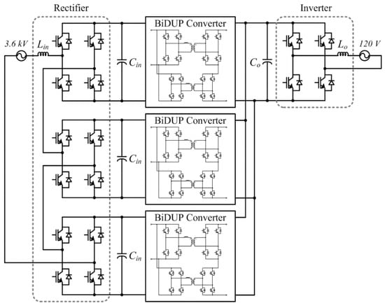
Figure 6.
The overall simulation structure of a 10 kVA-3.6 kV-120 V SST system.

Table 1.
Specification and parameters of the SST.
The cascaded multilevel rectifier consists of three H-bridge modules connected in series with separate dc-links (1.9 kV per each), which results in 7 voltage levels available for the synthesis of the input voltage. The H-bridge modules are controlled with the interleaved carrier-based PWM (Pulse Width Modulation) to achieve the multilevel operation and each PWM carrier is phase-shifted by 2π/3, respectively. The switching frequency of each H-bridge is 1.2 kHz, so that the effective switching frequency seen from the distribution grid is 7.2 kHz (1.2 kHz × 6) [19].
The main objectives of the cascaded multilevel rectifier are to maintain the high-voltage dc-link voltage (Vhdc) as constant as possible at its rated value by controlling the active power and to manipulate the power factor of the input ac grid side as required by controlling the reactive power. The overall PI (Proportional-Integral) controller-based control scheme is depicted in Figure 7a. The controller features two main loops: an inner line current control loop and an output dc-link voltage control loop. The dc-link voltages of the H-bridges are summed up first and controlled to maintain at 5.7 kV. A fast moving average filter, which has a time window corresponding to the period of the second harmonic ripple, is used to take into account the power fluctuation characteristic of a single-phase system [4]. The inner current controller uses the rotating reference frame (d-q coordinate system), which can be achieved by composing a hypothesized ac phase that lags the real ac phase by 90° [20] and obtaining the synchronizing (rotating) angle with a phase-locked loop (PLL) for a single-phase system; the d-axis current (id) controls the active power and the q-axis current (iq) controls the reactive power. Furthermore, the d-q current cross-coupling effect has been compensated and the d-q voltage components (vd and vq) have been feedfowarded to the final output voltage reference (vd* and vq*) to improve the dynamic performance of the system.
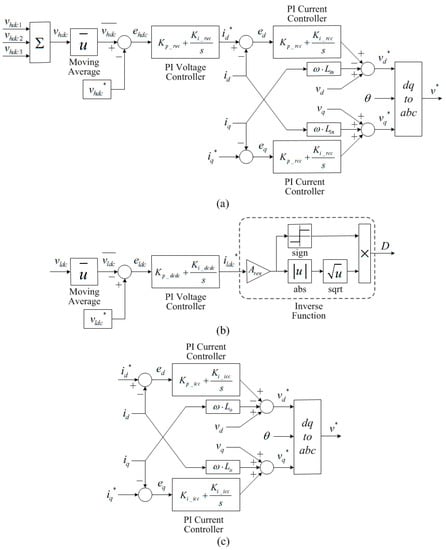
Figure 7.
The overall control schemes for the SST system. The PI controller-based control scheme for (a) the cascaded multilevel rectifier, (b) the BiDUP converter, and (c) the singe-phase full-bridge inverter.
The proposed BiDUP converter is connected to the dc-link of each H-bridge of the cascaded multilevel rectifier. The outputs of the BiDUP converters are connected in parallel and the switching signals are interleaved so that the frequency of the effective current ripple of the paralleled BiDUP converters becomes 21.6 kHz (3.6 kHz × 6).
The major responsibility of the BiDUP converter in the SST system is to maintain the low-voltage dc-link voltage as constant as possible at its rated value by controlling the power flow between the high-voltage-side rectifier and the low-voltage-side inverter. Figure 7b shows the overall control scheme for the BiDUP converter. Since the low-voltage side inverter is also a single-phase system and has the second harmonic power fluctuation, a fast-moving average filter is employed here again. Each BiDUP converter operates in DCM and it leads to a non-linear relationship between the average output current and the duty ratio as (9). Therefore, the BiDUP converter can be regarded as a non-linear actuator. To compensate the nonlinearity of the actuator, the inverse of the characteristic of the actuator, which is the inverse function of (9), can be used. Since the non-linearity has been compensated, a simple PI controller can be employed. Within the inverse function block, a signum function is used to distinguish the direction of power flow with the sign of the duty-ratio. In other words, the power flows from the primary side to the secondary side when the duty-ratio is a positive value, but from the secondary side to the primary side when negative.
The single-phase full-bridge inverter in the last stage is connected to the low-voltage dc-link. It is controlled by a simple carrier-based PWM and its switching frequency is 10.8 kHz. The inverter is in charge of providing active and reactive powers to the residential low-voltage ac grid as required. The overall control scheme is shown in Figure 7c, which is basically a current controller. The current controller uses the rotating reference frame which is synchronized with the phase angle of the low-voltage ac grid. Again, the d-axis current (id) controls the active power and the q-axis current (iq) controls the reactive power. An additional outer loop controller, such as a voltage controller and/or a frequency controller, might be included in the overall control scheme depending on application demands.
4. Simulation
To verify the feasibility of a SST system employing the BiDUP converter, the 10 kVA SST system designed in the previous section has been modelled and Matlab/Simulink and simulation studies have been performed. Table 2 summarizes the controller gains used in the simulation.

Table 2.
Controller gains.
Figure 8 shows the major voltage and current waveforms in the various parts of the SST system under a worst-case load scenario, where the residential ac grid does not consume any power from 0 to 0.12 s, and starts consuming and generating active power at its rated value from 0.12 to 0.4 s and from 0.4 to the end, respectively. Both the distribution and residential grids are assumed to consume 0 reactive power (iq* = 0 for both the grids). As it can be seen from the Figure 8a,d, both the line currents of the distribution grid and the residential grid are in phase with their line voltages during the consuming period, meanwhile, 180° out of phase during the generating period. At 0.12 s, the reference value of the d-axis current in the low-voltage inverter has been changed from 0 to 118 A in a step manner to start consuming the rated power. Due to the abrupt change of power flow, voltage dips are observable in both the high-voltage and low-voltage dc-link voltages and their minimum peak values are measured to be 5591 V (98.1%) and 189.1 V (94.6%), respectively. At 0.4 s, the reference value of the d-axis current in the low-voltage inverter has been changed from 118 A to −118 A in a step manner to start generating the rated power. Due to the abrupt change of power flow direction, voltage swells can now be observed in both the dc-link voltages and their maximum peak values are measured to be 5846 V (102.6%) and 210.5 V (105.3%), respectively. It is worth nothing that the ripple components in both the dc-link voltages are due to the power fluctuation characteristic of a single-phase system and the filtered dc-link voltages are used in the control.
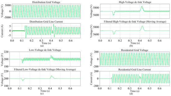
Figure 8.
The major voltage and current waveforms in the various parts of the SST system under the worst-case load scenario (id* = 0 from 0 to 0.12 s, id* = 118 from 0.12 to 0.4 s, and id* = −118 from 0.4 to 0.7 s); (a) Distribution grid voltage and current, (b) high-voltage-side dc-link voltage, (c) low-voltage-side dc-link voltage, (d) residential grid voltage and current.
Figure 9a shows the current waveforms within the BiDUP converters under the same load scenario. The upper subfigure shows the output current waveforms of the individual BiDUP converters and the lower subfigure shows the total output current in the paralleled output of the BiDUP converters. The polarity of the output current is positive during the power-consuming period but negative during the power-generating period. This confirms that the proposed BiDUP converter has a good bidirectional power flow capability. It is also worth noting that the ripple components due to the power fluctuation characteristic of a single-phase system also can be observed in the current waveforms. To take a closer look at the current waveforms, they are enlarged at one certain point during the consuming period and another point during the generating period as shown in Figure 9b,c, respectively. Now, the component output currents from the individual BiDUP converters can be observed more clearly. Each component current has an isosceles triangular shape and is evenly phase-shifted among each other. It can be observed from the total output current waveforms that their ripple sizes due to the DCM operation of the BiDUP have been substantially reduced by interleaving the component output currents.
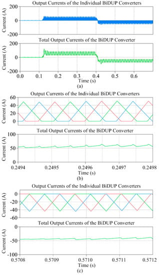
Figure 9.
The current waveforms within the BiDUP converters under the worst-case load scenario (id* = 0 A from 0 to 0.12 s, id* = 118 A from 0.12 to 0.4 s, and id* = −118 A from 0.4 to 0.7 s); (a) The overall output current, (b) enlarged waveform during consuming period, and (c) generating period.
One of the distinct advantages of the SST is its reactive-power regulation capability. Figure 10 shows the major voltage and current waveforms of the reactive-power regulation scenario, where the SST supplies 5 kW active power (50% of its rated power) from the distribution grid to the residential grid all through the simulation time, while 3 kVA (lagging, 30%) reactive power is supplied from 0.3 s in the residential grid and −3 kVA (leading) reactive power is supplied from 0.5 s in the distribution grid. Since the cross-coupling between the d-axis and q-axis currents are well compensated in the rectifier controller and the inverter controller, sudden changes in the reactive power references do not affect both the high-voltage and low-voltage dc-link voltages which is only related to the active power. As can be seen from Figure 10b,c, even though the ripple size of the second-order harmonic in the dc-link voltages changes, the average values of both the dc-link voltages are barely affected by sudden changes in the reactive-power reference.
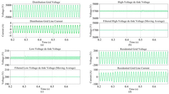
Figure 10.
The major voltage and current waveforms in the various parts of the SST system under the reactive-power regulation scenario (id* = 59 A from 0 to 0.7 s, for the residential grid iq* = 39.3 A (lagging) from 0.3 s, and for the distribution grid iq* = −1.3 A (leading) from 0.5 s); (a) Distribution grid voltage and current, (b) high-voltage-side dc-link voltage, (c) low-voltage-side dc-link voltage, (d) residential grid voltage and current.
Another distinct advantage of the SST system compared with the conventional transformers is the source disturbance refection capability. Figure 11 shows the major voltage and current waveforms of the input-voltage-sag scenario, where the SST supplies 5 kW active power (50% of its rated power) from the distribution grid to the residential grid all through the simulation time, while the 30% voltage sag occurs in the distribution grid from 0.3 to 0.6 s. As can be observed from Figure 11b, the sudden change in input voltage affects the high-voltage dc-link voltage. However, the proposed BiDUP dc-dc converter regulates its output voltage (low-voltage dc-link voltage) satisfactorily at the constant value of 200 V as shown in Figure 11c. Since the inverter produces its output with the well-regulated dc-link voltage, the power supply quality of the output voltage has not been affected by the input voltage-sag condition.
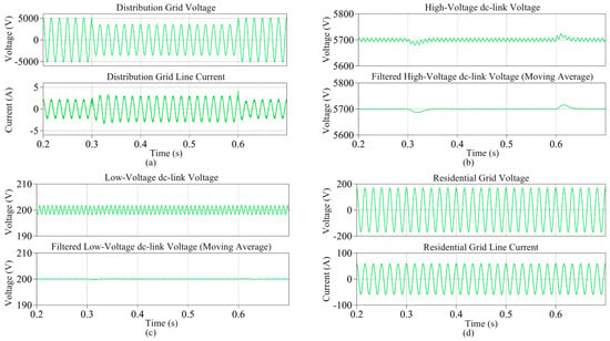
Figure 11.
The major voltage and current waveforms in the various parts of the SST system under the voltage-sag scenario (id* = 59 from 0 to 0.7 s, for the residential grid iq* = 39.3 (lagging) from 0.3 s, and for the distribution grid iq* = −1.3 (leading) from 0.5 s); (a) Distribution grid voltage and current, (b) high-voltage-side dc-link voltage, (c) low-voltage-side dc-link voltage, (d) residential grid voltage and current.
5. Experiments
A small-scale prototype for laboratory experiment has been built to verify the operational principle of the proposed BiDUP converter-based dc-dc converter as shown in Figure 12. The specifications for the prototype are summarized in Table 3.
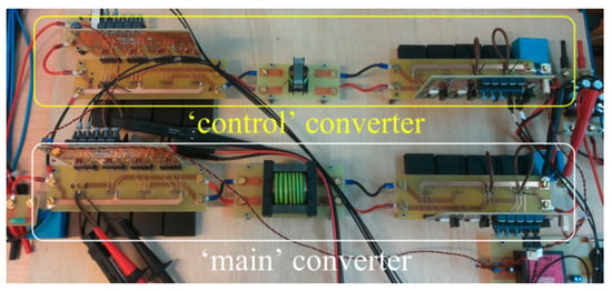
Figure 12.
A small-scaled prototype of the BiDUP converter for laboratory experiment.

Table 3.
Prototype specifications.
Figure 13 shows the experimental voltage and current waveforms in the transformers with positive duty-ratios of the ‘control’ converter. As it can be seen from the figure, the full-bridge of the ‘main’ converter always switches at its full duty ratio (0.5) regardless of the duty ratio of the ‘control’ converter. The transformer input current of the ‘main’ converter always reduces to zero before any switching occurs in the full bridge of the ‘main’ converter. In this way, the ZCS is always ensured in the ‘main’ converter. Furthermore, due to the filter inductance, the currents in both the ‘main’ and ‘control’ converters increase slowly when the IGBT is turning on. Hence, the IGBT turn-on switching losses are negligible in both the converters. However, the hard-switching occurs in the ‘control’ converter when the IGBT switches are turned off (indicated as ‘HS’ in the figure). Therefore, the major sources of the overall power loss in the BiDUP converter are the conduction loss in the ‘main’ converter and the turn-off switching loss in the ‘control’ converter.
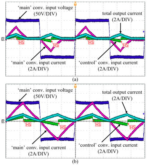
Figure 13.
Voltage and current waveforms in the transformers when the BiDUP converter operates in the forward mode with the ‘control’ converter duty-ratios of (a) 0.15 and (b) 0.25, respectively.
Figure 14 shows the experimental voltage and current waveforms in the transformers when the BiDUP converter operates in the backward mode with negative duty-ratios. Likewise with the forward operation mode, the full bridge of the ‘main’ converter always switches at its full duty ratio and its transformer current always reduces to zero before any switching, ensuring the ZCS in the ‘main’ converter. The ZCS is always achieved when the IGBT switches in both the ‘main’ and ‘control’ converters are turning on by the same token. Furthermore, the hard-switching still occurs in the ‘control’ converter when the IGBT switches are turned off as indicated in the figure. Therefore, the major sources of the overall power loss in the backward operation mode are identical to that of the forward operation. It should be noted that the total output currents are, now, negative values which indicates that the power is being transferred from the output side to the input side.
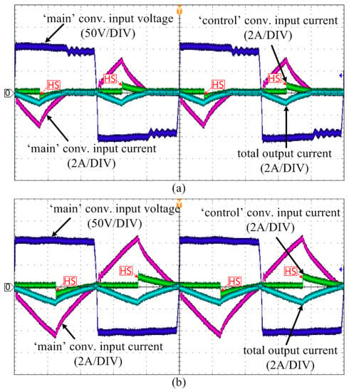
Figure 14.
Voltage and current waveforms in the transformers when the BiDUP converter operates in the backward mode with the ‘control’ converter duty-ratios of (a) −0.15 and (b) −0.25, respectively.
Figure 15 shows the voltage and current waveforms of each IGBT switch in the input-side of the ‘main’ and ‘control’ converters when the BiDUP converter operates in the forward mode with the ‘control’ converter duty-ratios of 0.15 and 0.25, respectively. Due to the filter inductance, the current in the ‘main’ converter increases slowly when the IGBT switch is turning on. The current increases slowly after the collector-emitter voltage drops to zero first. Therefore, the switching loss for the IGBT turn-on is negligible. When the switch is turning off, the current in the ‘main’ converter decreases near to zero first, and the voltage starts to increase. Therefore the switching loss for the IGBT turn-off in the ‘main’ converter is also very small. It is worth noting that the IGBT current in the ‘main’ converter never reaches zero when the switch turns off because there always exists the magnetization current of the transformer. However, the magnetization inductance of the transform is usually designed to be large enough to limit the amplitude of the magnetization current to a small value. Therefore, the switching loss will be very small too.
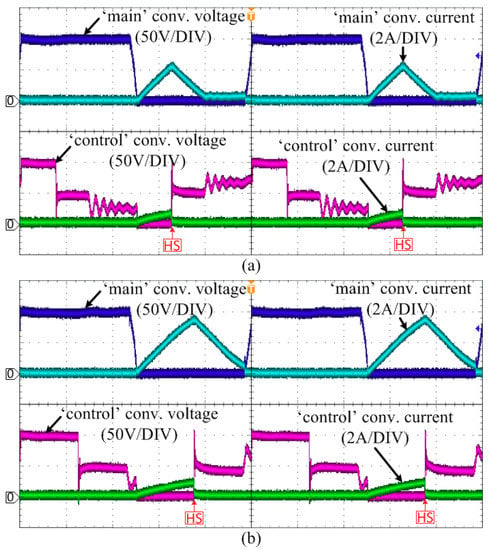
Figure 15.
Voltage and current waveforms in the IGBT switch (input-side) when the BiDUP converter operates in the forward mode with the ‘control’ converter duty-ratios of (a) 0.15 and (b) 0.25, respectively.
Likewise with the ‘main’ converter, when the IGBT is turning on, the current in the ‘control’ converter increases slowly due to the filter inductance. Therefore, the switching loss for the IGBT turn-on is negligible too. When the IGBT is turning off, however, the situation differs from the ‘main’ converter. The ‘control’ converter always performs hard-switching as indicated in the figure. Therefore, there exist turn-off switching losses due to the trailing current of the IGBT and the rapid increase of the collector-emitter voltage. This turn-off switching loss is the major cause of the overall switching losses of the BiDUP converter.
Figure 16 shows the voltage and current waveforms of each IGBT switch in the output-side of the ‘main’ and ‘control’ converters when the BiDUP converter operates in the backward mode with the ‘control’ converter duty-ratios of −0.15 and −0.25, respectively. Likewise with the forward operation, the current in the ‘main’ converter increases slowly after the collector-emitter voltage drops to zero first, so that the IGBT turn-on switching loss is negligible. In case of the switch turn-off, the current in the ‘main’ converter always decreases near to zero first, and then the voltage starts to increase. Hence, the switching loss for the IGBT turn-off in the ‘main’ converter is very small as well.
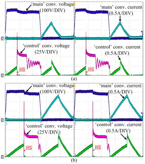
Figure 16.
Voltage and current waveforms in the IGBT switch (output-side) when the BiDUP converter operates in the backward mode with the ‘control’ converter duty-ratios of (a) −0.15 and (b) −0.25, respectively.
Likewise, when the IGBT is turning on, the current in the ‘control’ converter increases slowly due to the filter inductance. However, the ‘control’ converter always performs hard-switching when the IGBT switch is turning off as indicated in the figure. Therefore, there always exist turn-off switching losses in the ‘control’ converter. However, since the power processed by the ‘control’ converter itself is only a small portion of the overall power, the turn-off switching loss in the ‘control’ converter is not significant.
6. Conclusions
In this paper, a novel bidirectional double uneven power (BiDUP) converter based dc-dc converter and its design and control methods have been introduced. The main objectives of the proposed converter are to reduce both the switching losses in power semiconductor devices and the filter inductance requirement simultaneously. The proposed converter is expected to be highly beneficial for high-power applications where the dc voltage transformation is required. To verify the feasibility of the proposed converter for the high-power applications, a simulation study on the BiDUP converter based solid-state transformer (SST) in a distribution system has been presented. The simulation study has shown that the proposed BiDUP is capable of controlling its output voltage fast enough under various worst-case scenarios and, in turn, is suitable for the MV high-power SST application. Finally, a small-scale prototype and its experimental results have been presented to verify the operational principle of the proposed converter.
Author Contributions
K.-B.L. provided guidance and supervision. K.P. implemented the main research, performed the literature review, simulation, collecting technical details, wrote and revised the manuscript as well. All authors have equally contributed to the simulation results, reliability calculation and result discussions.
Funding
This research was supported by the KEPCO Research Institute under the project entitled by “Design of analysis model and optimal voltage for MVDC distribution systems (R17DA10) and “Human Resources Program in Energy Technology” of the Korea Institute of Energy Technology Evaluation and Planning (KETEP), granted financial resource from the Ministry of Trade, Industry & Energy, Republic of Korea. (No. 20174030201660).
Conflicts of Interest
The authors declare no conflict of interest.
References
- Brando, G.; Dannier, A.; Rizzo, R. Power electronic transformer application to grid connected photovoltaic systems. In Proceedings of the 2009 International Conference on Clean Electrical Power, Capri, Italy, 9–11 June 2009; pp. 685–690. [Google Scholar]
- Gupta, R.K.; Castelino, G.F.; Mohapatra, K.K.; Mohan, N. A novel integrated three-phase, switched multi-winding power electronic transformer converter for wind power generation system. In Proceedings of the 2009 35th Annual Conference of IEEE Industrial Electronics, Porto, Portugal, 3–5 November 2009; pp. 4481–4486. [Google Scholar]
- She, X.; Huang, A.Q.; Wang, F.; Burgos, R. Wind energy system with integrated functions of active power transfer, reactive power compensation, and voltage conversion. IEEE Trans. Ind. Electron. 2013, 60, 4512–4524. [Google Scholar] [CrossRef]
- Dujic, D.; Zhao, C.; Mester, A.; Steinke, J.K.; Weiss, M.; Lowdeni-Schmid, S.; Chaudhuri, T.; Stefanutti, P. Power electronic traction transformer-Low voltage prototype. IEEE Trans. Power Electron. 2013, 28, 5522–5534. [Google Scholar] [CrossRef]
- Zhao, C.; Dujic, D.; Mester, A.; Steinke, J.K.; Weiss, M.; Lowdeni-Schmid, S.; Chaudhuri, T.; Stefanutti, P. Power electronic traction transformer-Medium voltage prototype. IEEE Trans. Ind. Electron. 2014, 61, 3257–3268. [Google Scholar] [CrossRef]
- Qin, H.S.; Kimball, J.W. AC-AC dual active bridge converter for solid state transformer. In Proceedings of the 2009 IEEE Energy Conversion Congress and Exposition, San Jose, CA, USA, 20–24 September 2009; pp. 3039–3044. [Google Scholar]
- Abedini, A.; Lipo, T. A novel topology of solid state transformer. In Proceedings of the 2010 1st Power Electronic & Drive Systems & Technologies Conference (PEDSTC), Tehran, Iran, 17–18 February 2010; pp. 101–105. [Google Scholar]
- Glinka, M.; Marquardt, R. A new AC/AC multilevel converter family. IEEE Trans. Ind. Electron. 2005, 52, 662–669. [Google Scholar] [CrossRef]
- Sabahi, M.; Goharrizi, A.Y.; Hosseini, S.H.; Sharifian, M.B.; Gharehpetian, G.B. Flexible power electronic transformer. IEEE Trans. Power Electron. 2010, 25, 2159–2169. [Google Scholar] [CrossRef]
- Sabahi, M.; Hosseini, S.H.; Sharifian, M.B.; Goharrizi, A.Y.; Gharehpetian, G.B. Zero-voltage switching bi-directional power electronic transformer. IET Power Electron. 2010, 3, 818–828. [Google Scholar] [CrossRef]
- Bifaretti, S.; Zanchetta, P.; Watson, A.; Tarisciotti, L.; Clare, J.C. Advanced power electronic conversion and control system for universal and flexible power management. IEEE Trans. Smart Grid 2011, 2, 231–243. [Google Scholar] [CrossRef]
- Fan, H.F.; Li, H. High frequency transformer isolated bidirectional DC-DC converter modules with high efficiency over wide load range for 20 kVA solid-state transformer. IEEE Trans. Power Electron. 2011, 26, 3599–3608. [Google Scholar] [CrossRef]
- She, X.; Huang, A.Q.; Burgos, R. Review of solid-state transformer technologies and their application in power distribution systems. IEEE Trans. Emerg. Sel. Top. Power Electron. 2013, 1, 186–198. [Google Scholar] [CrossRef]
- Jovcic, D. Step-up dc-dc converter for megawatt size applications. IET Power Electron. 2009, 2, 675–685. [Google Scholar] [CrossRef]
- Ortiz, G.; Leibl, M.G.; Huber, J.E.; Kolar, J.W. Design and experimental testing of a resonant dc-dc converter for solid-state transformers. IEEE Trans. Power Electron. 2017, 32, 7534–7542. [Google Scholar] [CrossRef]
- Chen, H.; Divan, D. Soft-Switching Solid-State Transformer (S4T). IEEE Trans. Power Electron. 2018, 33, 2933–2947. [Google Scholar] [CrossRef]
- Park, K.; Chen, Z. A double uneven power converter-based dc-dc converter for high-power dc grid systems. IEEE Trans. Ind. Electron. 2015, 62, 7599–7608. [Google Scholar] [CrossRef]
- She, X.; Yu, X.; Wang, F.; Huang, A.Q. Design and demonstration of a 3.6-kV-120-V/10-kVA solid-state transformer for smart grid application. IEEE Trans. Power Electron. 2014, 29, 3982–3996. [Google Scholar] [CrossRef]
- Wu, B. High-Power Converters and AC Drives; Wiley-IEEE Press: Hoboken, NJ, USA, 2006; ISBN 978-0-471-73171-9. [Google Scholar]
- Yu, X.W.; Huang, A.Q.; Zhao, T.F.; Wang, G.Y. Coupling effect reduction of a voltage-balancing controller in single-phase cascaded multilevel converters. IEEE Trans. Power Electron. 2012, 27, 3530–3543. [Google Scholar]
© 2018 by the authors. Licensee MDPI, Basel, Switzerland. This article is an open access article distributed under the terms and conditions of the Creative Commons Attribution (CC BY) license (http://creativecommons.org/licenses/by/4.0/).