1. Introduction
With the development of society, the functionality and complexity of electronic devices is increasing. Frequency synthesizer, as a common signal generator, has been widely applied in many fields. Related researches have more and more requirements for the accuracy and stability of the frequency synthesizer, especially in the fields of satellite positioning, aerospace, surveying and mapping, guidance and high-speed communication [
1,
2]. The signal generator is a kind of instrument with a long history. With the birth of electronic technology, signal generation circuits have appeared in the 1920s. By the 1940s, there were standard signal generators that were mainly used to measure various receivers, and pulse signal generators were invented. Since the 1960s, signal generators have developed rapidly. In this period, analog electronics technology was generally used. The circuit of signal generators was composed of discrete components. RC and LC signal generation circuits play an important role in the development process. The RC circuit composed of resistor R and capacitor C can produce sine waves with continuous amplitude and adjustable frequency. The LC signal generating circuit composed of inductor L and capacitor C can produce less high-order harmonics and better output waveform. With the development of science and technology, digital circuits have entered the field of signal synthesis, and the way of signal synthesis has made rapid progress, many signal synthesis methods have been designed. Modern synthetic signal methods include direct analog frequency synthesis, phase-locked frequency synthesis and direct digital frequency synthesis. There are three kinds of synthesized frequency methods: direct analog frequency synthesis, phase-locked frequency synthesis and direct digital frequency synthesis [
3]. Direct analog frequency synthesis uses one or more different transistors to design RC oscillator or LC oscillator as reference signal sources, and the output signals are directly generated by frequency doubling, frequency division and mixing, and the signals obtained by this method have the characteristics of high frequency stability and fast frequency conversion. But both of the hardware debugging and the spurious suppression are not easy in the implementation of this method. Phase-locked frequency synthesis, also known as indirect synthesis method, uses one or more standard frequency sources to generate a large number of harmonics or combined frequencies by mixing and dividing harmonic generators. Then, the phase-locked loop (PLL) is used to lock the frequency of the voltage controlled oscillator (VCO) to a certain harmonic or combination frequency. The required frequency output is indirectly generated by a voltage-controlled oscillator. The advantage of this method is that the phase-locked loop is equivalent to a narrow band tracking filter. Therefore, it can select the desired frequency signal well, suppress the spurious components, and avoid the use of a large number of filters, which are conducive to integration and miniaturization. The disadvantage of this method is slow response [
4,
5]. Direct digital frequency synthesis is based on the concept of phase to synthesize frequencies and adopts the technology of digital sampling and storage. Because the direct digital synthesizer (DDS) is an open-loop system without any feedback link, the frequency conversion time is very short. Besides, the method can be realized digitally and conveniently, and it is small and light in weight. The DDS method in the design of frequency synthesizer has gradually become a mainstream method in the current field of electronic measurement and testing [
6].
Normally there are two main ways to design and implement a real frequency synthesizer. One is to use a dedicated DDS integrated chip to synthesize frequency. The other is to use FPGA to achieve DDS frequency synthesis. The first method is usually realized by using a microprocessor to drive the DDS integrated chip. In the given working mode of the DDS integrated chip, the internal circuit calculates the operating parameters of the kernel and synthesizes the frequency. Then, the analog signal is obtained by further processing by the later stage [
7,
8]. Due to the technical limitation of the DDS integrated chip, there are unavoidable performance defects in this kind of frequency synthesizer. The dedicated DDS integrated chip has a fixed number of phase accumulator bits and lacks flexibility. The number of its phase accumulators is relatively small, and the frequency resolution is relatively low. For example, we often use chip AD9913 to generate frequency signals. The bit width of its internal phase accumulator is 32 bits. When the reference frequency is 100 MHz, the resolution is 0.023 Hz. Even though 0.023 Hz is not a bad resolution for most applications, the typical accumulator-based DDS is not capable of generating some useful frequencies (like precisely 10 MHz) and cannot meet the high precision requirements of some special equipment or engineering [
9]. When expecting to get precisely 10 MHz, the AD9913 can only produce an approximate frequency of 9.999999986030161380 MHz.
FPGA is a new type of digital circuit. Its circuit function is programmable and customizable, which is different from the traditional integrated circuit with the structure and function of a fixed circuit. FPGA technology has overturned the traditional design, tape-out and packaging process of digital circuits. New digital circuits are developed directly on the finished FPGA chip. It overcomes the shortcomings of the internal structure of the DDS chip and improves the flexibility of the chip, which enlarges the user range and application fields of special digital circuits. Each logic gate in the FPGA chip performs a logical operation at every clock cycle. Therefore, FPGA is essentially a very large-scale parallel computing device, which is very suitable for developing DDS devices with high speed, high accuracy and high flexibility [
10]. The DDS device based on FPGA is usually composed of a phase accumulator, a waveform memory and a digital multiplier [
11,
12]. The phase accumulator accumulates the frequency tuning word loop to get the phase address; the size of the frequency tuning word determines the output frequency value; waveform memory stores a sampling point for a periodic output waveform; the phase address of the phase accumulator acts as the reading address of the waveform memory, from which the waveform sample points are taken out to form the digital waveform, and then the analog signal is obtained by further processing [
13].
As mentioned above, the frequency synthesis principles of the dedicated DDS integrated chip and the FPGA method are basically the same. Both of them use the phase accumulator to recursively sum the clock rate and frequency tuning word, and synthesize the frequency by means of the look-up table. The phase accumulator modulus of traditional DDS is usually a fixed value, and the frequency tuning words must also be positive integers, so this method can only synthesize a limited number of precise frequency signals. However, some practical projects and systems (as shown in
Figure 1) usually require precise frequency synthesizers to generate their reference frequency signals. Sometimes, these reference frequency signals must have a special frequency value. For example, in the communication system, in order to ensure the accuracy and effectiveness of information transmission, each base station generally needs to configure a communication clock subsystem. The communication clock subsystem is the basic guarantee for efficient and orderly operation of the whole system. A 5 MHz or 10 MHz frequency synthesizer is usually the frequency reference of these clock subsystems. Another example, the reference frequencies onboard satellite of some navigation satellite systems is 10.23 MHz. Any frequency error or deviation in the reference frequency will directly affect the navigation satellite system’s performance and such errors accumulated over time will result in a significantly large user ranging error varying up to several meters [
14]. These special frequency signals such as 5 MHz, 10 MHz and 10.23 MHz are hard to generate accurately by traditional DDS methods and devices. To solve this problem, a DDS method using compound frequency tuning word is designed and implemented in this paper, which is expected to further improve the accuracy of synthetic frequency under the condition of guaranteeing frequency stability.
2. Defects of Traditional DDS
The traditional DDS relies on the accumulator to recursively sum the frequency tuning word at the clock rate, obtaining the instantaneous value of the signal by means of a look-up table [
15]. As shown in
Figure 2, the method produces a time series of digital words at the output of the accumulator that increases linearly until the accumulator rolls over at its maximum value of
. Hence, the accumulator output has a fixed modulus
. Usually the accumulator output is truncated to
P-bits (using only the MSBs) to reduce the size and complexity of the angle-to-amplitude conversion block that immediately follows the accumulator. This causes the time series of digital words produced by the accumulator to appear at the input to the angle-to-amplitude converter as
P-bits words ranging in value from 0 to (
) [
16]. The accumulator output sequence range 0 to (
) maps to one revolution on the unit circle, that is, it linearly maps binary values from 0 to (
) to radian angles from 0 to 2π. This mapping arrangement allows the angle-to-amplitude converter to translate the
P-bits words to
Y-bits amplitude values (
Y) in a very efficient manner, and finally a low-pass filter is used to obtain a desired sinusoidal signal [
17].
The
Y-bits digital amplitude sequence signal output by the converter is converted into an analog signal by a
Y-bit DAC (Digital to Analog Converter, DAC) chip, and finally a low-pass filter is used to obtain a desired sinusoidal signal. We see the translation process relied on Equation (1):
where:
A is the signal amplitude;
P is the number of bits taken from the accumulator;
k is the binary value of those bits at any given instant;
x is the amplitude value corresponding to the address at a given time.
The following Equation expresses the frequency of the sinusoid that appears at the DAC output for a traditional accumulator-based DDS [
18]:
where:
is the synthesized frequency;
is the sampling frequency;
FTW is the frequency turning words;
.
The integer, frequency turning words, is a determining condition for controlling the output frequency. Since
FTW, by definition, is an integer, then
is constrained to the following set of frequencies:
Inspection of the Equation (3) indicates that the modulus of the DDS accumulator, determines both the frequency resolution of the DDS and the number of possible output frequencies. It can be seen that the ratio of the output frequency to the sampling frequency must satisfy:
Because the accumulator bit width is fixed, the frequency tuning word cannot be decimal, and the output frequency cannot be arbitrary value. Now for output frequencies that are integer submultiples of the sample rate (for example,
),
can be expressed as
(
Q is an integer). Substituting
for
in Equation (4) leads to:
Solving for
FTW yields
. Because
FTW and
Q must both be integers, the only values of
Q that satisfy Equation (5) can be expressed as
, where
K is an integer. In practical applications, the frequency tuning word that controls the output signal can be expressed as:
In the specific DDS implementation, it can be divided into two categories:
I. When the Equation (6) is satisfied, the DDS can output an accurate frequency. To demonstrate, assume that C is 32, Q = 16 = , FTW = 268,435,456, the available frequency turning word is an integer, and the address covers range from 0 to . When accumulating a loop, the next cycle returns to the initial value and the exact frequency value can be output.
II. When the Equation (6) is not satisfied, the frequency tuning word is a decimal number, and the actual accumulation takes an integer. After one cycle, the first sampling point cannot return to the initial point, so the sampling points of each period are different within a certain range, resulting in different waveform amplitudes and unstable waveforms. At the same time, there is phase loss after accumulating one cycle, the cycle increases, the frequency decreases, and an error occurs. For example, = 100 MH, = 10 MHz. In this case, , FTW = 429,496,729.6. A traditional accumulator-based DDS, regardless of the capacity of its accumulator, is not capable of synthesizing exactly 10 MHz. The closest frequency that a 32-bit accumulator-based DDS can get to 10 MHz with = 100 MHz is 9.99999998603016138 MHz, which is smaller than the expect value and has an absolute error of 0.01396983862 Hz. Such a frequency error is intolerable in some special precision equipment or engineering.
3. Accurate DDS Method Using Compound Frequency Tuning Word
Because the phase accumulator modulus of the traditional DDS is a fixed value, the frequency tuning word must also be a positive integer, which causes the traditional DDS method to only synthesize a finite number of precise frequency signals. In response to this problem, this paper proposes a DDS method using compound frequency tuning word. As visible in
Figure 3, the phase accumulator recursively sums the frequency tuning word component
X at a clock rate, and the obtained value is combined with the frequency tuning word components
A and
B of the auxiliary accumulator in the address generator. In the DDS method using the compound frequency tuning word, the compound frequency tuning word has three parts:
X,
A and
B. The main working process of the address generator is as follows: the frequency tuning word
X is added with a value
A after
B times of addition, and the subsequent operation is carried out on the basis of the new phase address. The
m-bits addresses are obtained by truncating the obtained address to the low bit, and it is sent to the phase-to-amplitude converter to output the
Y-bits amplitude of the address mapping. After the DA chip, the digital signal is converted into an analog signal, and finally the signal is filtered and amplified for output.
The Equation for calculating the exact DDS output frequency of the compound frequency tuning word:
where
M,
N are integers,
. The frequency ratio of the DDS method using compound frequency tuning word is very similar to that of the traditional DDS, but
N in the DDS of the compound frequency tuning word is not required to be a power of 2, it can be any integer.
The relationship between the output frequency of the DDS method using compound frequency tuning word and the sampling frequency is as follows:
In the Equation (8), the right end is a compound frequency tuning word,
X represents an integer part. After
N sampling, the difference between the actual phase and the maximum phase is
Y. In the DDS method using compound frequency tuning word, the processing of the fractional part is mainly added, so that the output frequency eliminates the error or minimizes the error. When the output frequency and the system clock are determined,
M and
N are unique in Equation (7) (
M and
N are mutual primes). The
X value (integer part) can be obtained by the Equation of the conventional DDS. Then find the remainder:
In Equation (9),
X is the frequency tuning word after rounding, the elements of
X to the nearest integers towards zero. After
N sampling, the difference between the actual phase and the maximum phase is the remainder, which will be further simplified:
In Equation (10), A and B are prime numbers, and both are integers. A and B are processed in the auxiliary accumulator in the DDS method using compound frequency tuning word.
When approximating M = 1, the corresponding N is a value near the actual number of sampling or the actual number of sampling when the address is overflowed. Assuming that is the actual number of sampling times for an address overflow, then is equal to the value near N or N, that is, the number of sampling times in a cycle completes a summation from 0 to the maximum address value, and when samples overflow for the next cycle, all sampling points in each cycle are coincident, then A is 0, B can be any positive integer, and the compound frequency control word is obtained. The compound frequency tuning word DDS can accurately output frequency. At this point, the phase difference between the two adjacent addresses is the phase represented by the low 16 bits of the accumulator.
If the sampling points of each cycle cannot overlap, DDS cannot accurately output the desired frequency. At this time:
I. If the simplification Equation (10) satisfies
and the
B value is a number less than 10, the compound frequency tuning word is
, after a period of sampling, the remainder is divided into uniform
B equal parts, it is evenly inserted into the whole sampling process, each time
A value is inserted, so that a period of sampling coverage range of 0 to
. All the sampling points in the next cycle coincide with the first sampling point to ensure that the sampling points in each cycle are exactly the same, and the DDS can output an accurate frequency. The method of inserting
A and
B values is shown in
Figure 4. For example, when the system clock = 100 MHz and the output frequency = 10 MHz,
C = 32, in this paper, the frequency tuning word = 429,496,729,
Y = 6,
M = 1,
N = 10,
A = 3 and
B = 5, they can be obtained, that is, the compound frequency tuning word
FTW = {429,496,729, 3, 5}. During the same period of sampling, the fourth sampling address is 4
X. The new sampling method is adopted, the fifth sampling address is (5
X + 3), and (5
X + 3) is the new addressing basis for the accumulation; The ninth sampling address is (9
X + 3), the tenth sampling address is (10
X + 6), that is the maximum value of the phase address, so that the sampling points in a cycle cover 0 to
, can ensure that the next cycle to take the same sampling points.
II. If the simplification Equation (10) does not satisfy , then the Equation (9) is approximately reduced to B less than 10 and a value of A is obtained. At this time, the compound frequency tuning word is , which ensures that the DDS synthesis frequency is closer to the expected value. For example, when the system clock = 100 MHz, the output frequency is required to be = 1.024 MHz, the frequency tuning word = 43,980,465 can be found. We can get , and the constraint can be used to meet the requirements of . Finding the compound frequency tuning word is = {43,980,465, 1, 9}, we can get a relatively high precision. In the two cases mentioned above, When the address is only X-accumulating, the phase difference between the two adjacent sampling points is the phase represented by the lower 16-bits in the accumulator. When the sample address is (X + A), the phase difference between the two adjacent sampling points is 16 bits plus A.
The main difference between the two methods is the different ways to generate addresses. The address of traditional DDS relies on the accumulator to recursively sum the frequency tuning word at the clock rate; The DDS method using compound frequency tuning word is under the control of the reference clock. When the frequency control word X is accumulated, each time B is accumulated, an A value is added to the address to get an adjustable address.
5. Experimental Results and Analysis
In the fields of power electronics and frequency standards, there are special requirements for the frequency synthesizer output frequency. For example, in order to meet the needs of battery monitoring and management of electric vehicles, Kadirvel K. et al. proposed an IC chip, whose maximum recommended clock drive value is just 2.048 MHz [
19]. In order to reduce the influence of the Dick effect, Wang et al. selected a 5 MHz signal with ultra-low phase noise as a reference of their microwave generator in the study of the influence of Dick effect in cold atomic clock in an integrating sphere [
20].
But in practical engineering applications, a traditional DDS cannot accurately synthesize a standard frequency signal. Suppose that the phase accumulator of the traditional DDS is 32 bits, the closest output frequency and its error when synthesizing special frequency points such as 1.024 MHz, 2.048 MHz 5 MHz, and 10 MHz are shown in
Table 1.
As shown in the third column of
Table 1, the frequency values represent the theoretical outputs of traditional DDS. In order to test the real performance of traditional DDS and the output stability and accuracy of the new DDS method proposed in this paper, we designed an experimental platform just as
Figure 8 shown.
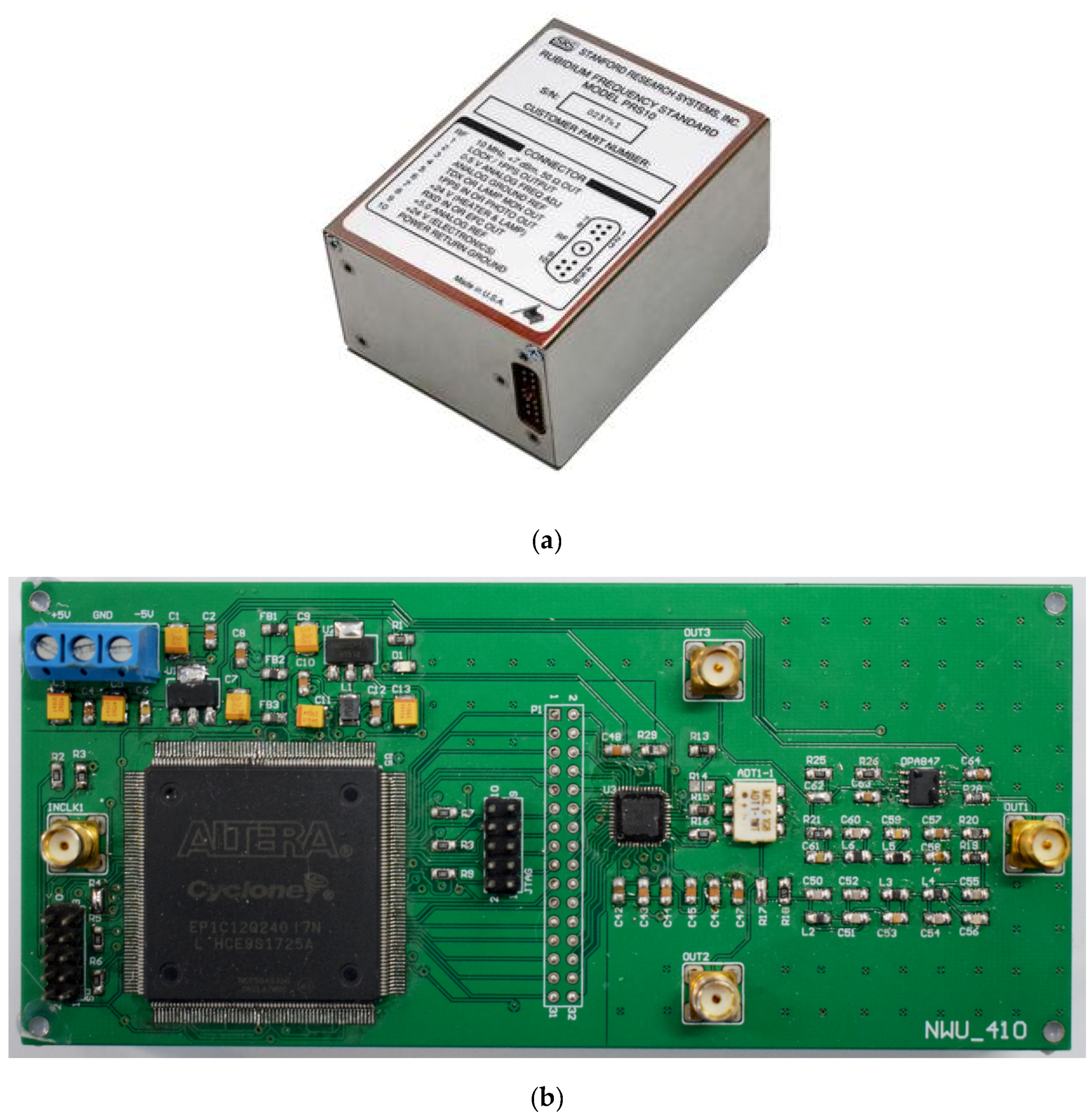
The platform mainly includes reference clock PRS10, distribution amplifier HP5087A, the FPGA implementation platform of DDS, Keysight 53220A counter, TimeLab test software and Stable32 test software. The photograph of the real experimental platform is shown as
Figure 8b. After the system is powered on for about 9 min, the frequency-locked circuit indicates that the rubidium clock outputs stable reference signal and can start the follow-up operation. The standard frequency source of the rubidium atomic clock is sent through a distribution amplifier to get two signals, one of which is input to the FPGA implementation platform of DDS as its standard frequency source. The other is input to the counter as its standard frequency source. The device under test and measuring equipment with common standard frequency source can ensure the credibility of the measurement results.
Then, the DDS method using the compound frequency tuning word is used to synthesize the frequency points of 1.024 MHz, 2.048 MHz, 5 MHz and 10 MHz. After nearly 11 h of measurement, its characteristics are analyzed. According to the test data, Stable32 is used to analyze the stability index of our new method. At the same time, experiments in
Figure 9 show that the DDS method using compound frequency tuning word has better stability. The stability test results for different frequency points show that the new DDS method proposed in this paper has a good stability index (short term stability as an example, better than 8.0 × 10
−12/s).
By using the same experiment platform shown in
Figure 7, the accuracy indexes of the DDS method using compound frequency tuning word and the traditional DDS frequency synthesis method are obtained and compared. The experiment results are shown in
Figure 10, the abscissa represents the average time of measurement and the ordinate represents the relative frequency difference. The experimental results show that the relative frequency deviation of the synthesized frequency is about 4.80 × 10
−12, which is three orders of magnitude lower than the traditional DDS frequency synthesis method (the relative frequency deviation is about 2.00 × 10
−9). It can be proved that the DDS using compound frequency tuning word has higher frequency output accuracy than the traditional DDS method.


