Article

Hardware Considerations for Tensor Implementation and Analysis Using the Field Programmable Gate Array

1
Department of Electronic and Computer Engineering, University of Limerick, V94 T9PX Limerick, Ireland
2
Department of Computer Science, College of Engineering and Applied Sciences, University at Albany, State University of New York, Albany, NY 12222, USA
*
Author to whom correspondence should be addressed.
Electronics 2018, 7(11), 320; https://doi.org/10.3390/electronics7110320
Submission received: 18 October 2018 / Revised: 7 November 2018 / Accepted: 8 November 2018 / Published: 13 November 2018
(This article belongs to the Special Issue Signal Processing and Analysis of Electrical Circuit)

Abstract

:
In today’s complex embedded systems targeting internet of things (IoT) applications, there is a greater need for embedded digital signal processing algorithms that can effectively and efficiently process complex data sets. A typical application considered is for use in supervised and unsupervised machine learning systems. With the move towards lower power, portable, and embedded hardware-software platforms that meet the current and future needs for such applications, there is a requirement on the design and development communities to consider different approaches to design realization and implementation. Typical approaches are based on software programmed processors that run the required algorithms on a software operating system. Whilst such approaches are well supported, they can lead to solutions that are not necessarily optimized for a particular problem. A consideration of different approaches to realize a working system is therefore required, and hardware based designs rather than software based designs can provide performance benefits in terms of power consumption and processing speed. In this paper, consideration is given to utilizing the field programmable gate array (FPGA) to implement a combined inner and outer product algorithm in hardware that utilizes the available hardware resources within the FPGA. These products form the basis of tensor analysis operations that underlie the data processing algorithms in many machine learning systems.

1. Introduction

Embedded system applications are today demanding greater levels of digital signal processing (DSP) capabilities whilst providing low-power operation and with reduced processing times for complex signal processing operations found typically in machine learning [1] systems. For example, facial recognition [2] for safety and security conscious applications is a noticeable every day example, and many smartphones today incorporate facial recognition software applications for phone and software app access. Embedded environmental sensors, as an alternative application, can input multiple sensor data values over a period of time and, using DSP algorithms, can analyze the data and autonomously provide specific outcomes. Although these applications may differ, within the system hardware and software, these are simply algorithms accessing data values that need to be processed. The system does not need to know the context of the data it is obtaining. Data processing is rather concerned with how effectively and efficiently it can obtain, store, and process the data before transmitting a result to an external system. This requires not only an understanding of regular access patterns in important internet of things (IoT) algorithms, but also an ability to identify similarities amongst such algorithms. Research presented herein shows how scalar operations, such as plus and times, extended to all scalar operations, can be defined in a single circuit that implements all scalar operations extended to: (i) n-dimensional tensors (arrays); (ii) the inner product, (matrix multiply is a 2-d instance) and the outer product, both on n-dimensional arrays (the Kronecker Product is a 2-d instance); and (iii) compressions, or reductions, over arbitrary dimensions. However, even more relationships exist. One of the most compute intensive operations in IoT is the Khatri-Rao, or parallel Kronecker Product, which, from the perspective of this research, is an outer product projected to a matrix, enabling contiguous reads and writes of data values at machine speeds.
In terms of the data, when this data is obtained, it must be stored in the available memory. This will be a mixture of cache memory within a suitably selected software programmed processor (microcontroller (µC), microprocessor (µP), or digital signal processor (DSP)), locally connected external volatile or non-volatile memory connected to the processor, memory connected to the processor via local area network (LAN), or via some form of Cloud based memory (Cloud storage). Identifying what to use and when is the challenge. Ideally, the data would be stored in specific memory locations so that the processor can optimally access the stored input data, process the data, and store the result (the output data) again in memory in suitable new locations, or overwriting existing data in already utilized memory. Knowing and anticipating cache memory misses, for example, enable a design that minimizes overhead(s), such as signal delays, energy, heat, and power.
In many embedded systems implemented today, the software programmed processor is the commonly used programmable device to perform complex tasks and interface to input and output systems. The software approach has been developed over the last number of years and is supported through tools (usually available via an integrated development environment (IDE)) and programming language constructs, providing the necessary syntax and semantics to perform the required complex tasks. However, increasingly, the programmable logic device (PLD) [3] that allows for a hardware configuration to be downloaded into the PLD in terms of digital logic operations is utilized. Figure 1 shows the target device choices available to the designer today. Alternatively, an application specific integrated circuit (ASIC) solution whereby a custom integrated circuit is designed and fabricated could be considered. Design goals include not only semantic, denotational, and functional descriptions of a circuit, but also an operational description (how to build the circuit and associated memory relative to access patterns of important algorithms).
In this paper, consideration is given to a general algorithm, and the resultant circuit, for an n-dimensional inner and outer product. This algorithm (circuit) builds upon scalar operations, thus creating a single IP (intellectual property) core that utilizes an efficient memory access algorithm. The field programmable gate array (FPGA) is used as the target hardware and the Xilinx® [4] Artix-7 [5] device is utilized in this case study. The two algorithms, the matrix multiplication, and Tensor Product (Kronecker Product), are foundational to essential algorithms in AI and IoT. The paper is presented in a way to discuss the necessary links between the computer science (algorithm design and development) and the engineering (circuit design, implementation, test, and verification) actions that need to be undertaken as a single, combined approach to system realization.
The paper is structured as follows. Section 2 will introduce and discuss algorithms for complex data analysis with a focus on tensor [6] analysis. An approach using tensor based computations with dimension data arrays that are to be developed and processed is introduced. Section 3 will discuss memory considerations for tensor analysis operations, and Section 4 will introduce the use of the FPGA in implementing hardware and hardware/software co-design realizations of tensor computations. Section 5 will provide a case study design created using the VHDL (Very High Speed Integrated Circuit (VHSIC) Hardware Description Language (HDL)) [7] for synthesis and implementation within the FPGA. The design architecture, simulation results, and physical prototype test results are presented, along with a discussion into implementation possibilities. Section 6 will conclude the paper.

2. Algorithms for Tensor Analysis

2.1. Introduction

In this section, data structures using tensor notation are introduced and discussed with the need to consider and implement high performance computing (HPC) applications [8], such as required in artificial intelligence (AI), machine learning (ML), and deep learning (DL) systems [9]. The section commences with an introduction to tensors and then followed by a discussion into the use of tensors in HPC applications. The algorithms foundational to IoT (Matrix Multiply, Kronecker Product, and Compressions (Reductions)) are targeted with the need for a unified n-dimensional inner and outer product circuit that can optimally identify and access suitable memories to store input and processed data.

2.2. Tensors as Algebraic Objects

As the need for IoT [10] and AI solutions grows, so does the need for High Performance Tensor (HPT) operations [11]. Tensors often provide a natural and compact representation for multidimensional data. For example, a function with five parameters can be thought of as a five-dimensional array. This is a particularly useful approach to structuring complex data sets for analysis.
With the complexity of tensor analysis requirements in real-world scenarios, there is a need for suitable hardware and software platforms to effectively and efficiently perform tensor analysis operations. Although there is a plethora of tensor platforms available for use, all the platforms are built upon tensors using various software programming languages, approaches, and performances. Selecting and obtaining the right programming language and hardware platform to run tensor computation programs on is not a trivial task. Fortunately, numerous efforts are underway to identify hot spots and build firmware and hardware. These efforts are built upon over 10 years of national and international workshops (e.g., [12,13]) uniting scientists to address these issues.
Tensors are algebraic objects that describe linear and multi-linear relationships. Tensors can be represented as multidimensional arrays. A tensor is denoted by its rank from 0 upwards. Each rank represents an array of a particular dimension. This idea is shown in Table 1 that identifies the tensor rank, its mathematical entity, and an example realization using the Python language [14], using Python lists to hold the data (in the examples, using integer numbers). A scalar value representing a magnitude (e.g., the speed of a moving object) is a tensor of rank 0. A rank 1 tensor is a vector representing a magnitude and direction (e.g., the velocity of a moving object: Speed and direction of motion). Matrices (n × m arrays) have two dimensions and are rank 2 tensors. A three-dimensional (n × m × p) array can be visualized as a cube and is a rank 3 tensor. Tensors with ranks greater than 3 can readily be created and analysis performed on the data they hold would be performed by accessing the appropriate element within the tensor and performing a suitable mathematical operation before storing the result in another tensor.
In a physical realization of this process, the tensor data would be stored in a suitable size memory, the data would be accessed (typically using a software programmed processor), and the computation would be undertaken using fixed- or floating-point arithmetic. This entire process should, ideally, stream data contiguously, and ideally anticipate where cache memory misses might occur, thus minimizing overhead up and down the memory hierarchy. For example, in an implementation using cache memory, L1 cache memory miss could also miss in L2, L3, and Page memory.
A tensor rank, or a tensor’s dimensionality, can be thought of in at least two ways. The more traditional way being, as the number of rows and columns change in a matrix, so does the dimension. Even with that perspective, computation methods often decompose such matrices into blocks. Conceptually, this can be thought of as “lifting” the dimension of an array. Further blocking “lifts” the dimension even more. Another way of viewing a tensor’s dimensionality is by the number of arguments in a function input over time. The most general way to view dimensionality is to combine these attributes. The idealized methods for formulating architectural components are chosen to match the arithmetic and memory access patterns of the algorithms under investigation. In this paper, the n-dimensional inner and outer products are considered. Thus, in this case, what might be thought of as a two-dimensional problem can be lifted to perhaps eight or more dimensions to reflect a physical implementation, considering the memory as registers, the levels of cache memory, RAM (random access memory), and HDD (hard disk drive). With that formulation, it is possible to create deterministic cost functions validated by experimentation, and, ideally, an idealized component construction can be realized that meets desired goals, such as heat dissipation, time, power, and hardware cost.
When an algorithm is run, the hardware implementing the algorithm will access available memory. In Figure 2, a prototypical graph of how an algorithm that does not have cache memory misses or page memory faults is presented. The shape of the graph changes as it moves through the memory hierarchy. This identifies the time requirements associated with the different memories from L1 cache memory through to disk (HDD). Note the change in the slope with memory type. The slope reflects how attributes, such as speed, cost, and power, would affect performance. Algorithm execution (memory access) time is, however, relative to the L1 cache memory chosen. For example, it could be nanoseconds, microseconds, milliseconds, seconds, minutes, or hours as the data moves further up the memory hierarchy. Often, performance is related to a decrease in arithmetic operations, i.e., a reduction of arithmetic complexity. In an ideal computing environment, where memory and computation would have the same costs, this would be the case. Unfortunately, it is also necessary to be concerned with the cost of data input/output (I/O). In parallel to this, it is a necessity to consider memory access patterns and how these relate to the levels of memory. Pre-fetching is one way to alleviate delays. However, often the algorithm developer must rely on the attributes of a compiler and hope the compiler is pre-fetching data in an optimum manner. The developer must trust that this action is performed correctly. This is becoming harder to achieve given that machines are becoming ever more complex and compiler writers are getting scarcer. Empirical methods of experimentation reveal graphs, such as the one shown in Figure 2. Such diagnostic methods allow the algorithm developer to observe the performance of a particular algorithm running on a machine. It is then possible to look at memory speed, size, and other cost factors to put together a model of how we might improve performance through “dimension lifting”. That said, the goal is always to try to keep the slope linear, i.e., the linear part of a polynomial curve such that the slope is minimized.
Presently, the goal is to achieve a situation where the graph is polynomial, avoiding exponential behavior, such as the one in Figure 2, using HDDs. A co-design approach, complemented with dimension lifting and analysis, as discussed above, can be used to calculate upper and lower bounds of algorithms relative to their data size, memory access patterns, and arithmetic. The goal is to ensure performance stays as linear as possible. This type of information enables the algorithm developers insight into what memories to select for use, i.e., what type and size of memory should be used to keep the slope constant. This, of course, would include pre-fetching, buffering, and timings to feed the prior levels at memory speed. If this is not possible, given the available memory choices, the slope change can be minimized.

2.3. Machine Learning, Deep Learning, and Tensors

Tensor and machine learning communities have provided a solid research infrastructure, reaching from the efficient routines for tensor calculus to methods of multi-way data analysis, i.e., from tensor decompositions to methods for consistent and efficient estimation of parameters of probabilistic models. Some tensor-based models have the characteristic that if there is a good match between the model and the underlying structure in the data, the models are much more interpretable than alternative techniques. Their interpretability is an essential feature for the machine learning techniques to gain acceptance in the rather engineering intensive fields of automation and control of cyber-physical systems. Many of these systems show intrinsically multi-linear behavior, which is appropriately modeled by tensor methods, and tools for controller design can use these models. The calibration of sensors delivering data and the higher resolution of measured data will have an additional impact on the interpretability of models.
Deep learning is a subfield of machine learning that supports a set of algorithms inspired by the structure and function of the human brain. TensorflowTM [15], PyTorch [16], Keras [17], MXNet [18], The Microsoft Cognitive Toolkit (CNTK) [19], Caffe [20], Deeplearning4j [21], and Chainer [22] are machine learning frameworks that are used to design, build, and train deep learning models. Such frameworks continue to emerge. These frameworks support numerical computations on multidimensional data arrays, or tensors, e.g., point-wise operations, such as add, sub, mul, pow, exp, sqrt, div, and mod. They also support numerous linear algebra operations, such as Matrix-Multiply, Kronecker Product, Cholesky Factorization, LU (Lower-Upper) Decomposition, singular-value decomposition (SVD), and Transpose. The programs would be written in various languages, such as Python, C, C++, and Java. These languages also include libraries/packages/modules that have been developed to support high-level tensor operations, in many cases under the umbrellas of machine learning and deep learning.

2.4. Tensor Hardware

Google’s introduction of a Tensor Processing Unit (TPU) [23] that works in conjunction with TensorFlow emphasizes that there is a need for fast tensor computation. That need will only grow exponentially as the use of AI increases. Consequently, what would an idealized processor for tensors look like? What would idealized software defined hardware look like? What are important pervasive algorithms? Two workshops, one at the NSF (National Science Foundation) [12] in America, and another at Dagstuhl [13], validated and promoted how tensors are used in numerous domains, considering AI and IoT in general. Charles Van Loan, a co-organizer of the NSF Workshop, emphasized the importance of The Kronecker Product. He called it the Product of the Times. The algorithm (circuit) presented herein is foundational to this very important algorithm. The goal is to develop designs that could be used to build a Universal Algebraic Unit© (UAU©) that could support all the mathematics in numerical libraries, such as NumPy, which most, if not all, applications mentioned above, use and rely on for performance. There are two challenges in the design and development of applications that require tensor support: Optimal software and hardware, necessitating a co-design approach. Due to the ubiquitous nature of tensors, a co-design approach is used to achieve the goals of the work.

2.5. Contribution of this Paper

This paper demonstrates the Matrix Multiplication and Kronecker Product that are both built from a common algorithm, the outer product. This design is unique in that is provides:
  • A general approach to inner and outer product, n dimensional, 0 ≤ n;
  • a general approach relative to scalar operations other than + and ×; and
  • a demonstration of how the design enables speed-up for Kronecker Products
The design presented in this paper is for an n-dimensional inner and outer product, e.g., for 2-d matrix multiply, which builds upon the scalar operations of + and × [24]. Some operations may be realized in hardware, firmware, or software. This generalized inner product is defined using reductions and outer products [24], and reduces to three loops independent of conformable argument dimensions and shapes. This is due to Psi Reduction, where it is possible to, through linear and multilinear transformations, reduce an array expression to a normal form. Then, through “dimension lifting” of a normal form, idealized hardware can be realized where the size of buffers relative to speed and size of connecting memories, DMA (Direct Memory Access) hardware (contiguous and strided), and other memory forms, when a problem size is known, or conjectured, and details of hardware are available and known.

2.6. The Kronecker Family of Algorithms

With an ability to build an idealized Kronecker Product, it is possible to address multiple Kronecker Products, parallel Kronecker Products, and outer products of Kronecker Products. These algorithms are used throughout the models built by mathematicians. Moreover, they are often used many times in sequence, necessitating an optimization study. If strides are required, as in the classical approach, performance will suffer. The Kronecker Product is viewed as an outer product, no matter how many there are in an expression. Consequently, it is not necessary to be concerned with strided access until the end when the outer product result is transposed and reshaped, thus saving energy and time. It is then possible to capitalize on contiguous access streaming from component to component. The analysis may consider time, space, speed, and other parameters, such as energy and heat, to determine cost.

3. Memory Considerations for Tensor Analysis

3.1. Introduction

In order to understand memory considerations, it is important to understand the algorithms that dominate tensor analysis: Inner Products (Matrix Multiply), and Outer Products (Kronecker or Tensor Product). Others include transformations and selections of components. Models in AI and IoT [13] are dominated by multiple Kronecker Products, parallel Kronecker Products (Khatri-Rao), and outer products of Kronecker Products (Tracey Singh), in conjunction with compressions over dimensions. Memory access patterns are well known. Moving on from an algorithmic specification to an optimized software or hardware instantiation of that algorithm requires maximizing the data structures that represent the algorithm in conjunction with the memory(ies) of a computer.

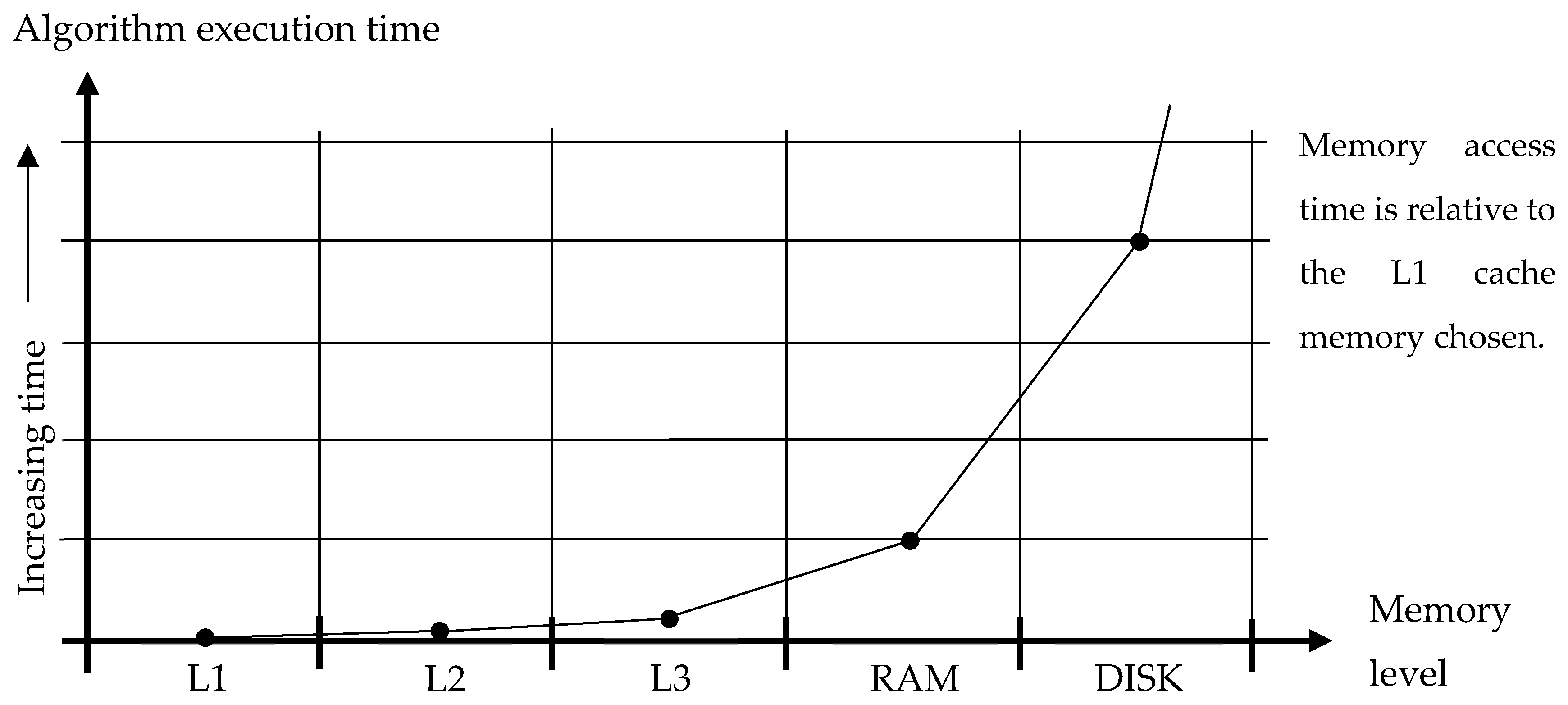
3.2. Computer Memory Access

From the onset of computing, computer scientists and mathematicians have discussed the complexity of an algorithm that translates to finding the least amount of arithmetic to perform. In an ideal world, where memories had the same speed no matter where they were, the computation effort would be based on the complexity of the algorithm. In fact, in the early days of computing, that was the case where memory was only one clock cycle away from the CPU (central processing unit). This is not true now. Now, what matters is the least amount of arithmetic and an optimal use of memory. From an engineering point of view, this means an understanding of the algorithm operation from a memory access pattern perspective. Moreover, through that understanding, it is possible to create an optimal, predictive, and reproducible performance.

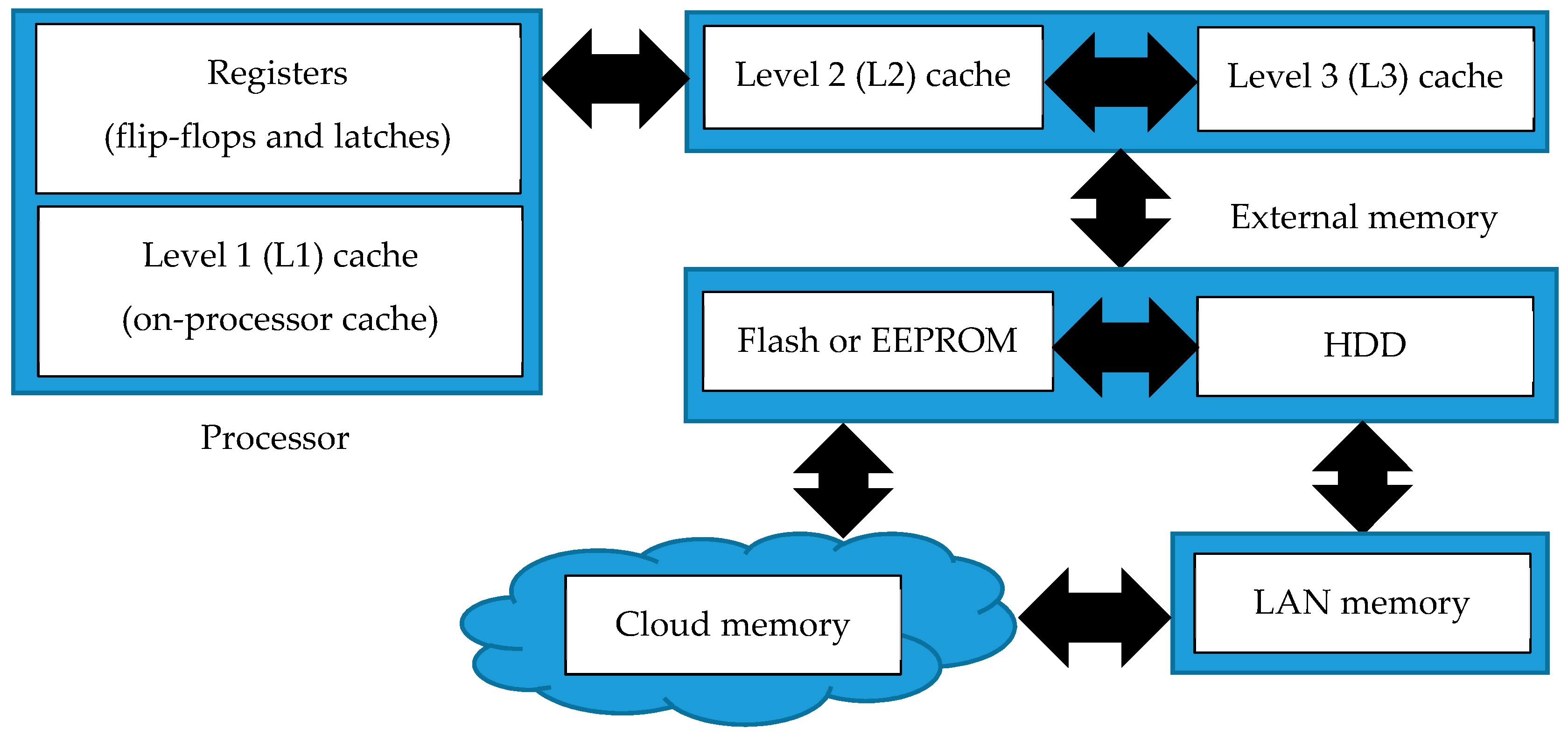
3.3. Cache Memory: Memory Types and Caches in a Typical Processor System

Over the years, memory has become faster in conjunction with memory types becoming more diverse. Architectures now support multiple, non-uniform memories, multiple processors, and multiple networks, and those architectures are combined to form complex, multiple networks. In an IoT application, there may be a case that one application requires the use of a substantial portion of the available resources and those resources must have a reproducible capacity. Figure 3 presents a view of the different memories that may be available in an IoT application, from processor to the Cloud. This view is based on a software programmed processor approach. Different memory types (principle of operation, storage capacity, speed, cost, ability to retain the data when the device power supply is removed (volatile vs. non-volatile memory), and physical location in relation to the processor core) would be considered based on the system requirements. The fastest memories with the shortest read and write times would be closest to the processor core, and are referred to as the cache memory. Figure 3 considers the cache memory as three levels (L1, L2, and L3), where the registers are closest to the core and on the same integrated circuit (IC) die as the processor itself before the cache memory would be accessed. L1 cache memory would be SRAM (static RAM) fabricated onto the same IC die as the processor, and would be limited in the amount of data it could hold. The registers and L1 cache memory would be used to retain the data of immediate use by the processor. External to the processor would be external cache memory (L2 and L3), where this memory may be fast SRAM with limited data storage potential or slower dynamic RAM (DRAM) that would have a greater data storage potential. RAM is volatile memory, so for data retention when the power supply is removed, non-volatile memory types would be required: EEPROM (electrically erasable programmable read only memory), Flash memory based on EEPROM, and HDD would be local memory followed by external memory connected to a local area network (a “network drive”) and Cloud memory. However, there are costs associated with each memory type that would need to factored into a cost function for the memory.

3.4. Cache Misses and Implications

To help understand why cache memory misses, page faults, and other memory faults cause delays in computation, reference to the 1-d fast Fourier transform (FFT) can be made. Theory states that a length n FFT has an n log n complexity and so an idealized computation time could be determined from this assumption. However, the computation could take significantly longer to complete, depending on a number of hardware related issues that include the availability of cache memory, the associativity of the cache, how many levels of memory there are, and the size of the problem. For example, if a four-way associative cache is used, a radix 4 FFT might be selected based on the size of the available associative cache. However, suppose a radix 2 is used. If the input vector for the FFT was 0 1 2 3 4 5 6 7 8 9 10 11 12 13 14 15, and the cache could fit only the first eight values, that means that on the 4th cycle, there is a cache miss. Knowing that the data could be reshaped and transposed to obtain data locality, i.e., 0 8 1 9 2 10 3 11 4 12 5 13 6 14 7 15, the operation could be completed with the data locally stored. However, as the input data set size increases, this not only results in cache misses, it also results in page faults, significantly slowing down the performance of an algorithm, which can be viewed graphically as an exponential rise [25]. For signal processing applications, the implication is that there will be a computation time increase.

3.5. Cost Functions for Memory Access

Usually cost functions are based on statistical methods. However, the analysis used in this work create a Normal Form that depicts the levels of memory desired relative to the access patterns of algorithms. With this, it is possible, a priori, to define the implementation requirements, such as maximum heat dissipation, power, cost, and time. With this information, as an FPGA designer, it is possible to utilize the available hardware resources and add the right types and levels of memory, the number of FPGAs linked together, and use FPGAs with other forms of processing unit. Such considerations would come from knowledge of the hardware and knowledge of algorithm requirements. Through experimental methods, developed by one of the co-authors, it can be seen that each level of memory as a Normal Form moves through the memory relative to its access patterns and arithmetic. What can be seen for any algorithm is that the curves, referring to Figure 2, start out constant, but then move to become a linear curve(s) while computation is still in real memory. Then, it is noticed that for each small piece of linearity, the slope gets steeper, indicating a change in memory speed. Thus, an evolution of a polynomial curve is seen that finally goes exponential when the access is to HDD. In parallel, if the available sizes and speeds of the various architectural components available, such as registers, buffers, and memories, are known, then it is possible to “dimension lift” the Normal Form to include all these attributes. Thus, performance can be predicted and verified via suitably designed experiments.

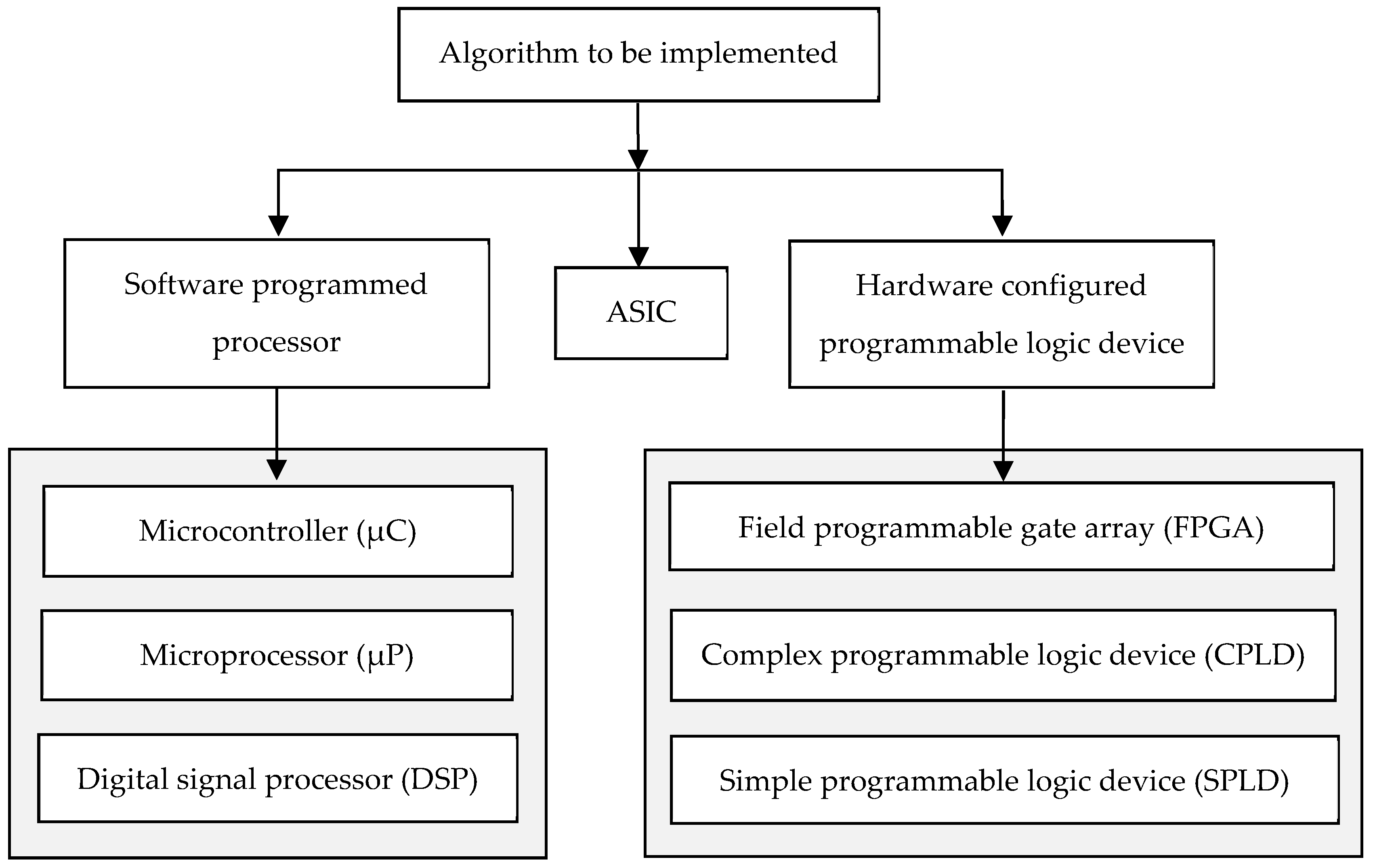
4. The Field Programmable Gate Array (FPGA)

4.1. Introduction

In this section, the FPGA is introduced as a configurable hardware device that has an internal circuit structure that can be configured to different digital circuit or system architectures. It can, for example, be configured to implement a range of digital circuits from a simple combinational logic circuit through to a complex processor architecture. With the available hardware resources and ability to describe the circuit/system design using a hardware description language (HDL), such as VHDL or Verilog [26], the designer can implement custom design architectures that are optimized to a set of requirements. For example, it is possible to describe a processor architecture using VHDL or Verilog, and to synthesize the design description using a set of design synthesis constraints into a logic description that can then be targeted to a specific FPGA device (design implementation, “place and route”). This processor, which is hardware, would then be connected to a memory containing a program for the processor to run, the memory may be registers (flip-flops), available memory macros within the FPGA or external memory devices connected to the pins of the FPGA. Therefore, it would be possible to implement a hardware only design or a hardware/software co-design. In addition, if adequate hardware resources were available, more than one processor could be configured into the FPGA and a multi-processor device therefore developed.

4.2. Programmable Logic Devices (PLDs)

The basic concept of the PLD is to provide a programmable (configurable) IC that enables the designer to configure logic cells and interconnect within the device itself to form a digital electronic circuit that is housed within a single packaged IC. In this, the hardware resources (the available hardware for use by the designer) will be configured to implement a required functionality. By changing the hardware configuration, the PLD will operate a different function. Hardware configured PLDs are becoming increasingly popular due to the potential benefits in terms of logic potential (obsolescence), rapid prototyping capabilities in digital ASIC design (early stage prototyping, design debugging, and performance evaluation), and design speed benefits, where PLD based hardware can implement the same functions as a software programmed processor, but in a reduced time. Concurrent (parallel) operations can be built into the PLD circuit configuration that would otherwise be implemented sequentially within a processor. This is particularly important for computationally expensive mathematical operations, such as the FFT, digital filtering, and other mathematical operations that require complex data sets to be analyzed in a short time. Table 2 summarizes available devices and their vendors. It is not, however, a trivial task to select the right device for a specific application or range of applications.

4.3. Hardware Functionality within the FPGA

Each FPGA provides a set hardware resources available to the designer where the use of specific resources would be considered to obtain a required performance in a specific application. However, this does rely on the use of the correct FPGA for the application and the knowledge of the designer in using these available hardware resources.
There are specific advantages in selecting an FPGA for use rather than an off-the-shelf processor. By selecting the appropriate hardware architecture, high speed DSP operation, such as digital filtering and FFT operations, can be achieved, which might not be possible in software. This is partly due to the ability to create a custom design architecture and partly due to concurrent operation, which means that operations in hardware can be run in parallel as well as sequentially. A typical FPGA also has a high number of digital input and output pins for connecting to peripheral devices with programmable I/O standards. This allows for flexibility in the types of peripheral devices, such as memory and communications ICs, that could be connected to the FPGA. Within the device, as well as programmable logic circuits, built-in memories for data storage are available, which have an immediate and temporary use, i.e., for cache memory scenarios. The DSP operations are supported using built-in hardware multipliers, and fast fixed-point and floating-point calculations can be implemented. In some FPGAs, built-in analog-to-digital converters (ADCs) are available for analog input sampling as well as IP blocks, such as FFT and digital filter blocks. These resources give the ability to develop a custom design architecture suited to the specific application. The FPGA is configured by downloading a design configuration as a sequence of binary logic values (sequence of 0’s and 1’s). The configuration would be initially created as a file using the FPGA design tools that is then downloaded into the device. The configuration values are stored in memory within the device, where the memory may be volatile or non-volatile:
  • Volatile memory: When data are stored within the memory, the data are retained in the memory whilst the memory is connected to a power supply. Once the power supply has been removed, then the contents of the memory (the data) are lost. The early FPGAs utilized volatile SRAM based memory.
  • Non-volatile memory: When data are stored within the memory, the data are retained in the memory even when the power supply has been removed. Specific FPGAs available today utilize Flash memory for holding the configuration.

5. Inner and Outer Product Implementation in Hardware Using the FPGA Case Study

5.1. Introduction

In this section, the design, simulation, and physical prototype testing of a single IP core that implements the inner and outer products are presented. The idea here is to have a hardware macro cell, or core, that can be accessed from an external digital system (e.g., a software programmed processor that can pass the computation tasks to this cell whilst it performs other operations in parallel). The input array data are stored as constants within arrays in the ipOpCore module, as shown in Figure 4, and are therefore, in this case, read-only. However, in another application, then it would be necessary to allow the arrays to be read-write for entering new data to be analyzed and then the design would be modified to allow array A and B data to be loaded into the core, either as serial or parallel data. Hence, the discussion provided in this section relates to the specific case study. In addition, a single result output could be considered and the need for test data output might not be a requirement. The motivation behind this work is to model tensors as multi-dimensional arrays and to analyze these using tensor analysis in hardware. This requires a suitable array access algorithm to be developed, the use of suitable memory for storing data in a specific application, and a suitable implementation strategy. In this paper, the inner and outer products are only considered using the FPGA as the target device, an efficient algorithm to implement the inner and outer products in a single circuit implemented in hardware is used, and appropriate embedded FPGA memory resources to enable fast memory access are used.
The design shown in Figure 4 was created to allow for both product results to be independently accessed during normal runtime operation and for specific internal data to be accessed for test and debug purposes. The design description was written in VHDL as a combination of behavioral, RTL, and structural code targeting the Xilinx® Artix-7 (XC7A35TICSG324-1L) FPGA. This specific device was chosen for practical reasons as it contains hardware resources suited for this application. The design, however, is portable and is readily transferred to other FPGAs, or to be part of a larger digital ASIC design, if required. For any design implementation, the choice of hardware, and potentially software, to use would be based on a number of considerations. The FPGA was mounted on the Digilent® Arty A7-35T Development Board and was chosen for the following reasons:
The FPGA considered is used in other project work and as such, the work described in this paper could readily be incorporated into these projects. Specifically, sensor data acquisition using the FPGA and data analysis within the FPGA projects would benefit from this work where the algorithm and memory access operations used in this paper would provide additional value to the work undertaken.
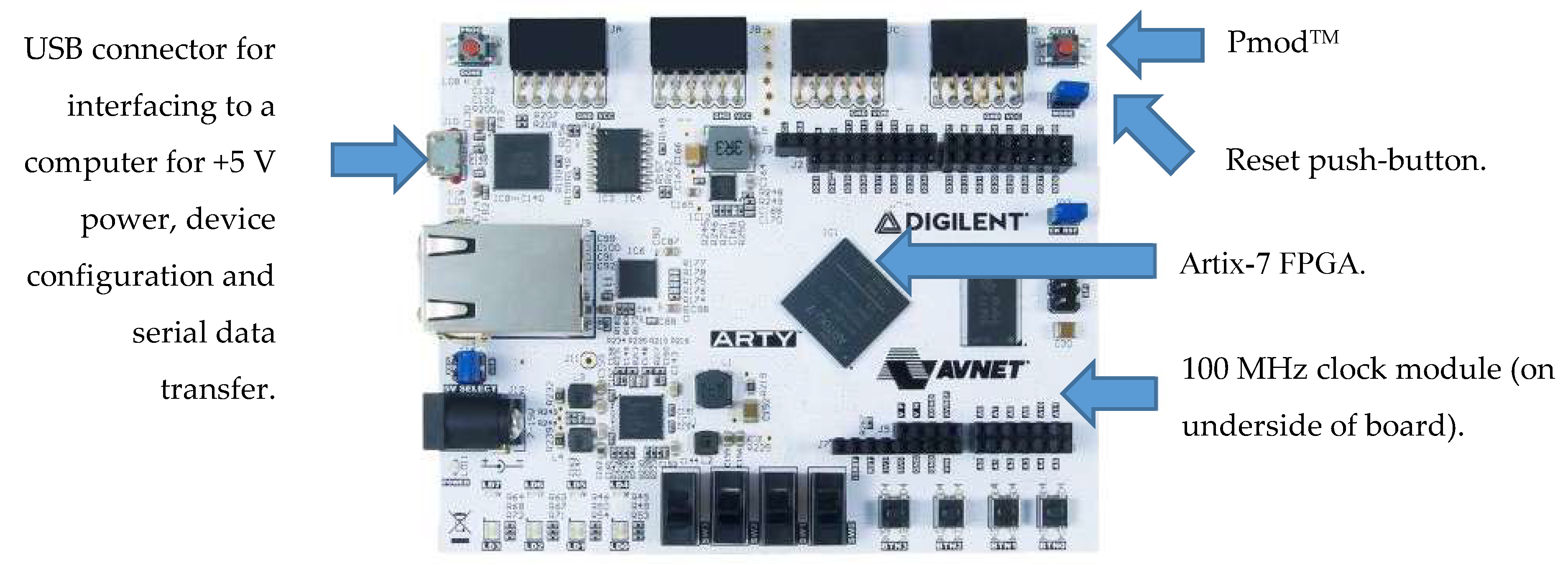
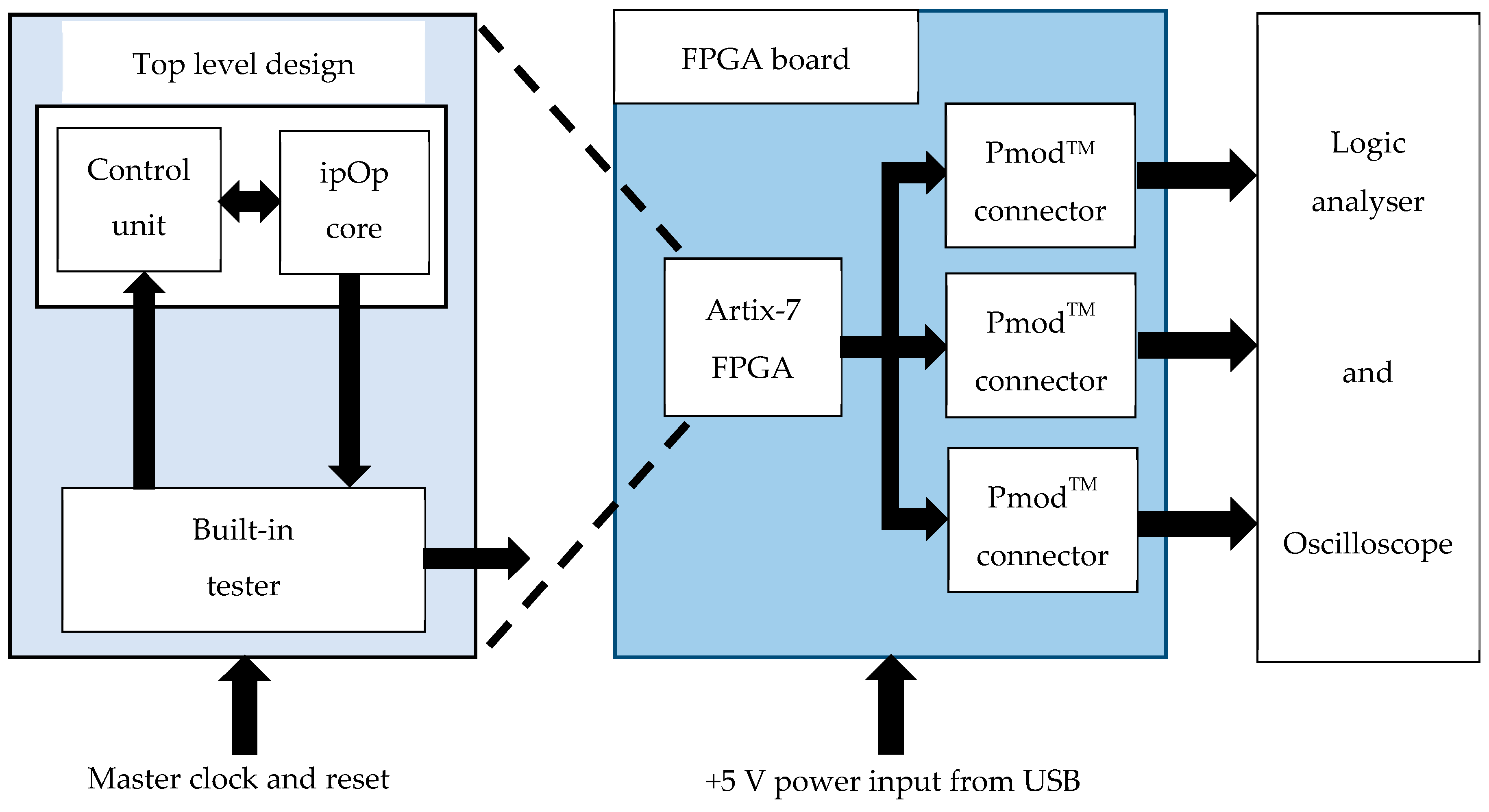
  • The development board used provided hardware resources that were useful for project work, such as the 100 MHz clock, external memory, switches, push buttons, light emitting diodes (LEDs), expansion connectors, LAN connection, and a universal serial bus (USB) interface for FPGA configuration and runtime serial I/O.
  • The development board was physically compact and could be readily integrated into an enclosure for mobility purposes and operated from a battery rather than powered through the USB +5 V power.
  • The Artix-7 FPGA provided adequate internal resources and I/O for the work undertaken and external resources could be readily added via the expansion connectors if required.
  • For memory implementation, the FPGA can use the internal look-up tables (LUTs) as distributed memory for small memories, can use internal BRAM (Block RAM) for larger memories, and external volatile/non-volatile memories connected to the I/O.
  • For computation requirements, the FPGA allows for both fixed-point and floating-point arithmetic operations to be implemented.
  • For an embedded processor based approach, the MicroBlaze CPU can be instantiated within the FPGA for software based implementations.
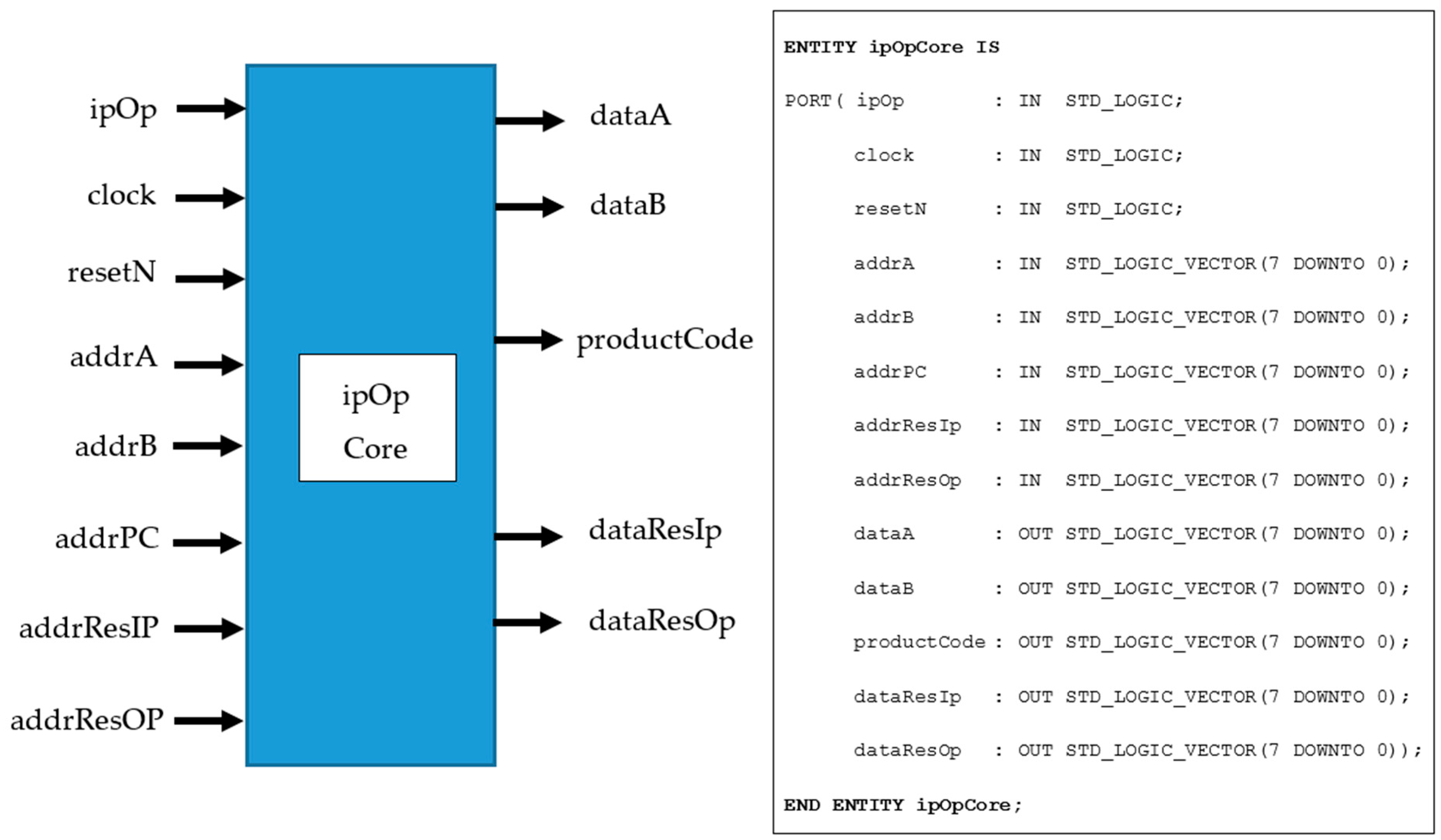
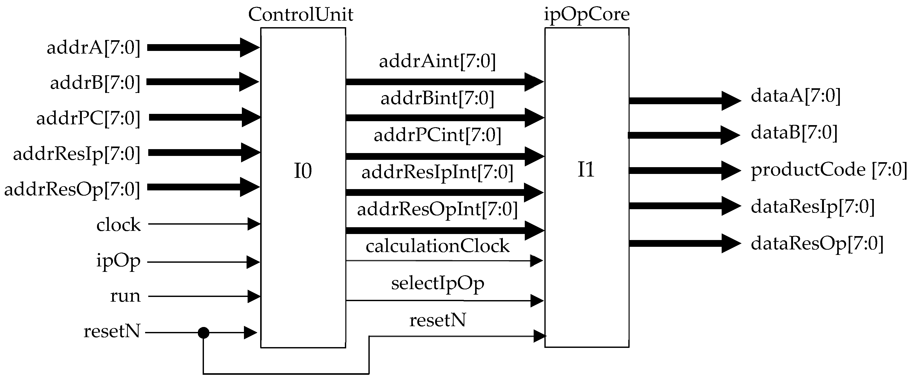
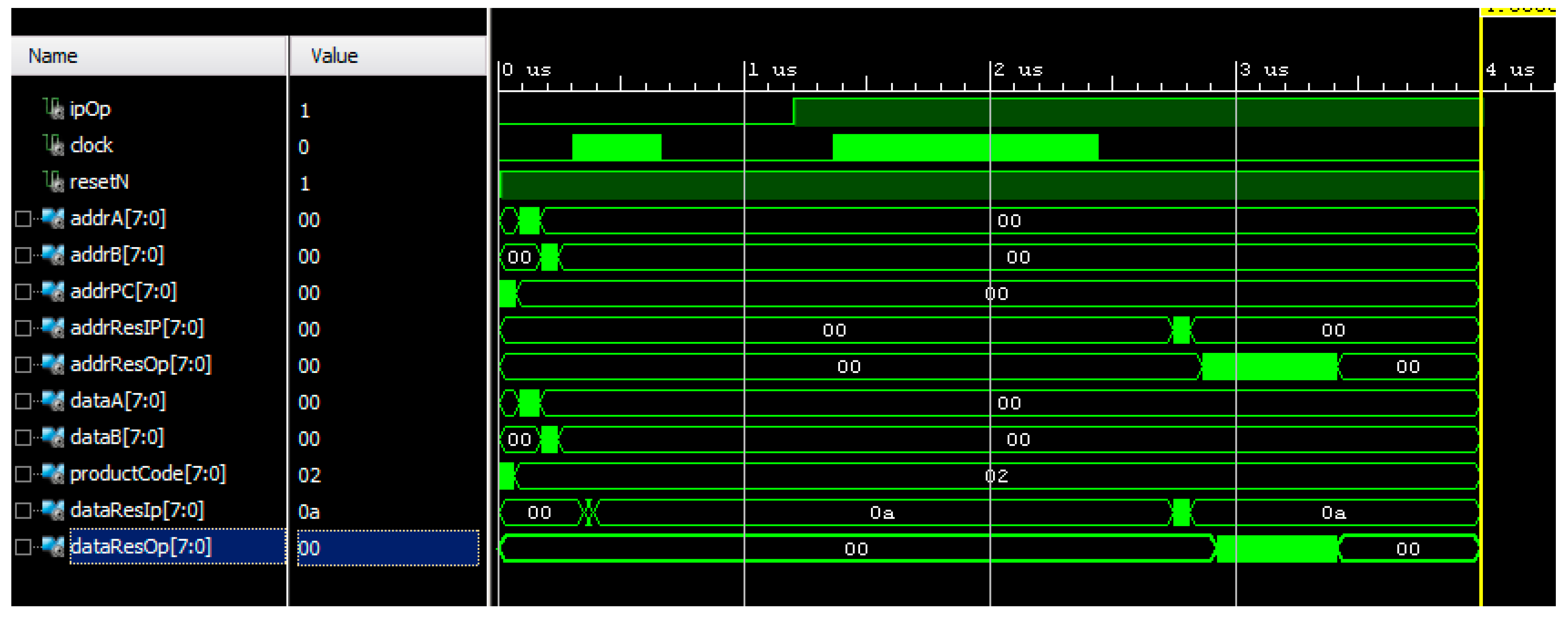
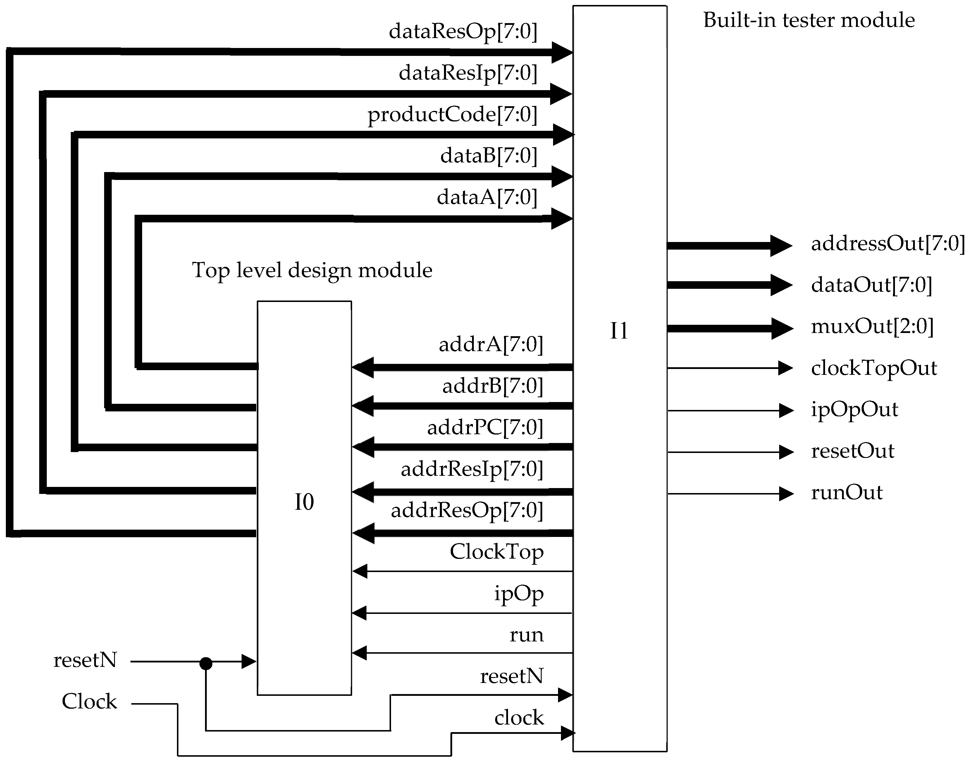
The I/O for this module are as follows:
ipOpUser to select whether the inner or outer product is to be performed.
clockMaster clock (100 MHz).
resetNMaster, asynchronous active low reset.
addrAArray A address for reading array contents (input tensor A).
addrBArray B address for reading array contents (input tensor B).
addrPCArray PC address for reading array contents (product code array).
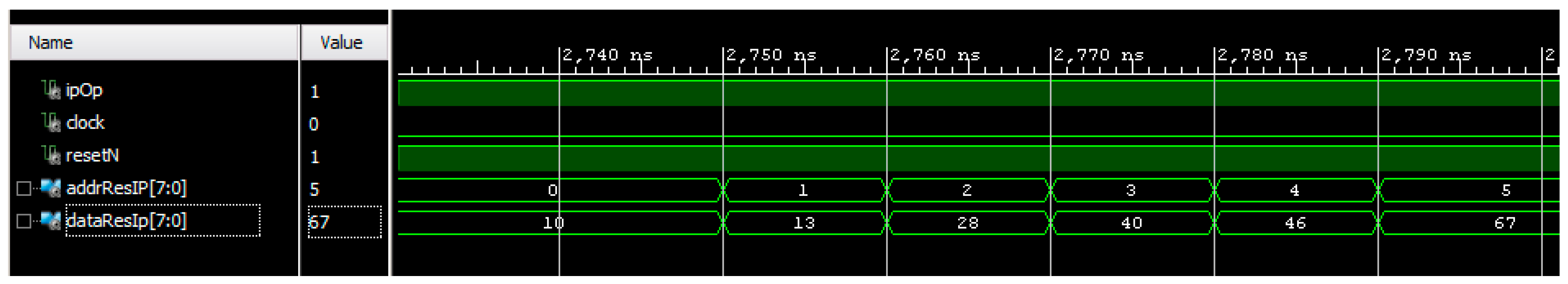
addrResIpAddress of inner product for reading array contents (output tensor IP).
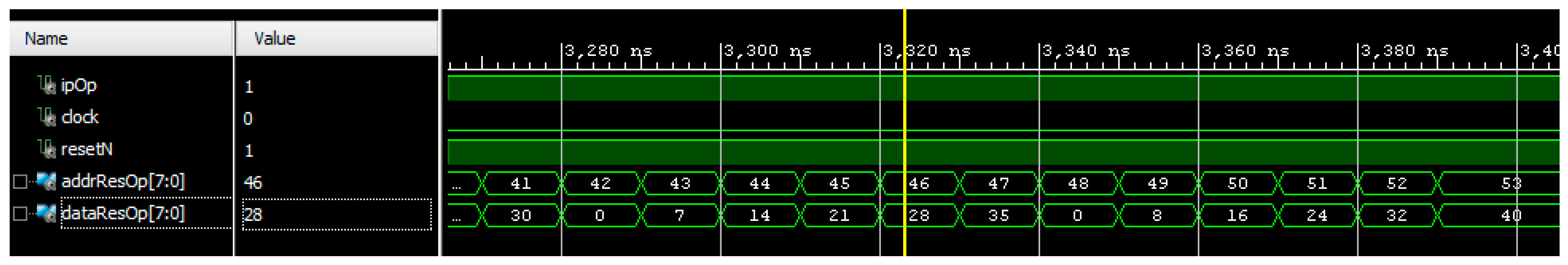
addrResOpAddress of outer product for reading array contents (output tensor OP).
dataAArray A data element being accessed (for test purposes only).
dataBArray B data element being accessed (for test purposes only).
productCodeInput array size and shape information for algorithm operation.
dataResIpInner product result array (Serial read-out).
dataResOpOuter product result array contents (serial readout).
These I/O signals can be categorized as input control, input address, and output data.

5.2. Design Approach and Target FPGA

The operation of the combined inner and outer product is demonstrated by reference to a case study design that implements the necessary memory and algorithms functions within a single IP core. Given that these functions are to be mapped to a custom design architecture and configured within the FPGA, a range of possible solutions can be created. The starting point for the design is the computation to perform. Consider the tensor product of two arrays (A and B), where A is a 3 × 3 array and B is a 3 × 2 array. For demonstration purposes, the numbers are limited to being 8-bit signed integers rather than real numbers. The principle of evaluation is the same for both number types, but the HDL coding style to be adopted would be different. Therefore, the possible numbers considered would be integer values in the range of −12810 to +12710. Internally within the VHDL code, these values were modelled as INTEGER data types that were suitable for simulation and synthesis. For synthesis, the integer numbers were translated to an 8-bit wide STD_LOGIC_VECTOR data type. This meant that the physical digital circuit utilized an 8-bit data bus and this size bus was selected as a standard width for all array input addresses and output data. Fixed-point, 2′s complement arithmetic was also implemented. Whilst the data range was limited in size, this approach was chosen as the purpose of the work was to implement and demonstrate the algorithm and memory utilization. The VHDL code was written such that the data range and array sizes were readily adjusted within the array definitions and no modification to the algorithm code was required. Floating-point arithmetic rather than fixed-point arithmetic could be used by coding a floating-point multiplier for matrix multiplication operations (e.g., [28,29]), and modelling the data as floating point numbers rather than simple fixed-point scalar numbers as used here. Considering arrays A and B, these two arrays can be operated on to form the tensor product as both the inner product and the outer product:
A = [ 0 1 2 3 4 5 6 7 8 ]         B = [ 0 1 2 3 4 5 ]
The tensor product for A and B is noted as:
C = A     B
The result of the inner product, Cip, is:
C i p = A     B = [ 10 13 28 40 46 67 ]
The result of the outer product, Cop, is:
C o p = A     B = [ 0 0 0 1 0 2 0 0 2 3 4 6 0 0 4 5 8 10 0 3 0 4 0 5 6 9 8 12 10 15 12 15 16 20 20 25 0 6 0 7 0 8 12 18 14 21 16 24 24 30 28 35 32 40 ] .
The above products were initially developed using C and Python coding where the data in C were stored in arrays and in Python were stored in lists. The combined inner/outer product algorithm was verified through running the algorithm with different data sets and verifying the software simulation model results with manual hand calculation results. Once the software version of the design was verified, the Python code functionality was manually translated to a VHDL equivalent. The two key design decisions to make were:
  • How to model the arrays for early-stage evaluation work and how to map the arrays to hardware in the FPGA.
  • How to design the algorithm to meet timing constraints, such as maximum processing time, number of clock cycles required, hardware size considerations, and the potential clock frequency, with the hardware once it is configured within the FPGA.
In this design, the data set was small and so VHDL arrays were used for both the early-stage evaluation work and for synthesis purposes. In VHDL, the input and results arrays were defined and initialized as follows:
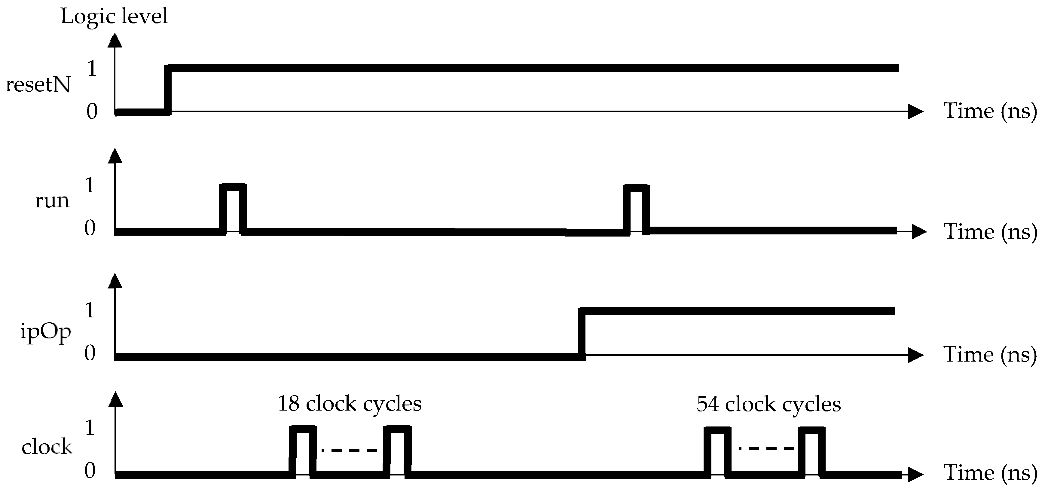
TYPE array_1by4 IS ARRAY (0 TO 3) OF INTEGER;
TYPE array_1by6 IS ARRAY (0 TO 5) OF INTEGER;
TYPE array_1by9 IS ARRAY (0 TO 8) OF INTEGER;
TYPE array_1by36 IS ARRAY (0 TO 35) OF INTEGER;
TYPE array_1by54 IS ARRAY (0 TO 53) OF INTEGER;
 
CONSTANT arrayA      : array_1by9 := (0, 1, 2, 3, 4, 5, 6, 7, 8);
CONSTANT arrayB      : array_1by6 := (0, 1, 2, 3, 4, 5);
 
SIGNAL arrayResultIp   : array_1by6 := (0, 0, 0, 0, 0, 0);
SIGNAL arrayResultOp   : array_1by54 := (0, 0, 0, 0, 0, 0, 0, 0, 0,
                          0, 0, 0, 0, 0, 0, 0, 0, 0,
                          0, 0, 0, 0, 0, 0, 0, 0, 0,
                          0, 0, 0, 0, 0, 0, 0, 0, 0,
                          0, 0, 0, 0, 0, 0, 0, 0, 0,
                          0, 0, 0, 0, 0, 0, 0, 0, 0);
These are one-dimensional arrays suited for ease of memory addressing, appropriate for the algorithm operation, synthesizable into logic, and have a direct equivalence in the C and Python software models. The input arrays (arrayA and arrayB) contain the input data. The results arrays (arrayResultIp (inner product) and arrayResultOp (outer product)) were initialized with 0′s. It was not necessary, in this case, to map to any embedded BRAM or external memory as the data set size was small and easily mapped by the synthesis tool to distributed RAM within the FPGA. The PC (product code) array is not shown above, but this is an array that contains the shape and size of arrays, A and B. For the algorithm, with direct mapping to VHDL from the Python code, the inner product and outer product each required a set number of clock cycles. Figure 5 shows a simplified timing diagram identifying the signals required to implement the inner/outer product computation. Once the computation has been completed, the array contents could then be read out one element at a time. For evaluation purposes, all array values were made accessible concurrently, but could readily be made available serially via a multiplexor arrangement to reduce the number of output signals required in the design.
A computation run would commence with the run control signal being pulsed 0-1-0 with the product selection input ipOp set to either logic 0 (inner product) or logic 1 (outer product). In this implementation, the inner product required 18 clock cycles and the outer product required 54 clock cycles to complete. The array data read-out operations are not, however, shown in Figure 5. The data values were defined using the INTEGER data type for modelling and simulation purposes, and these values were mapped to an 8-bit STD_LOGIC_VECTOR data type for synthesis into hardware. The 8-bit width data bus was sufficient to account for all data values in this study.

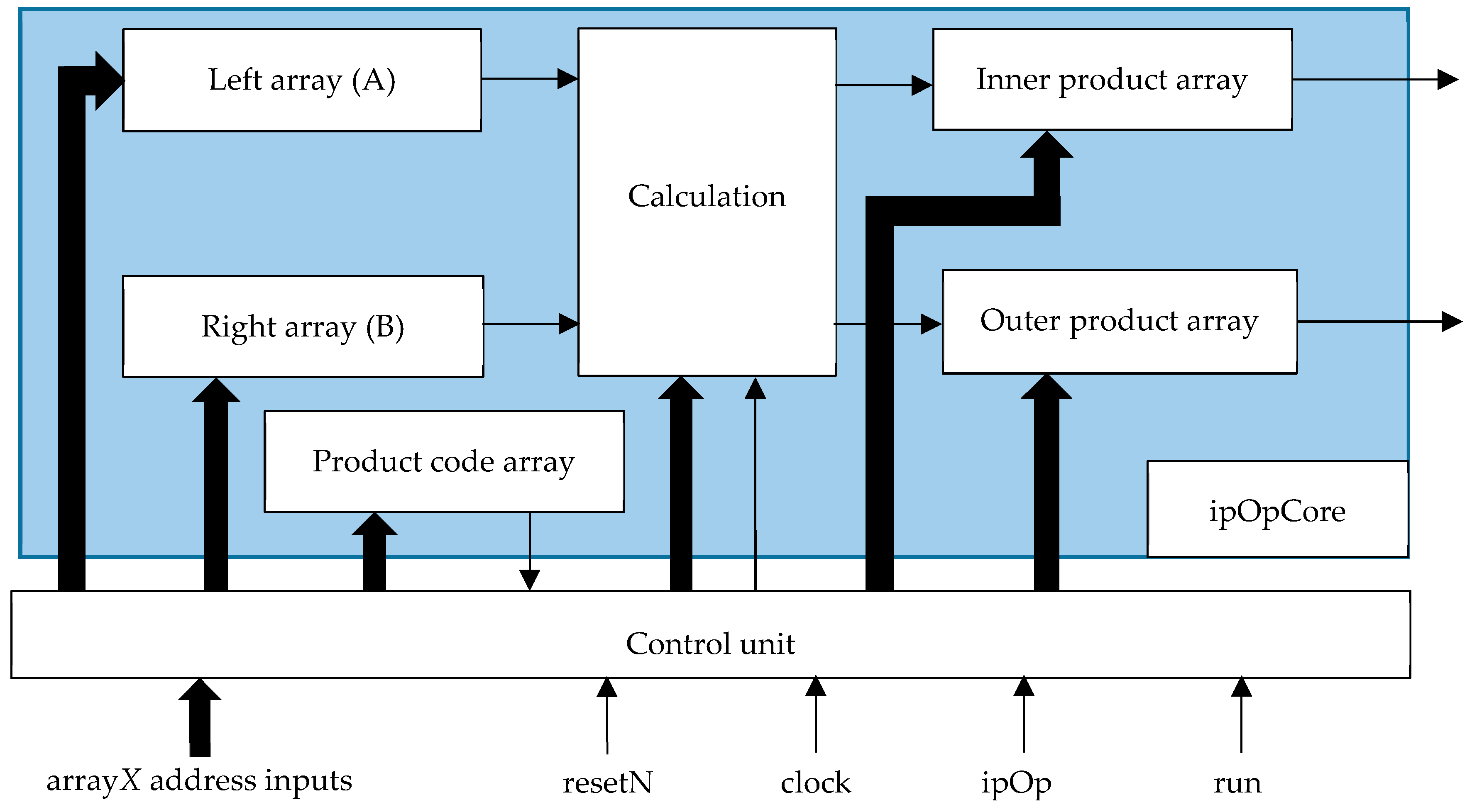
5.3. System Architecture

How the memory and algorithm would generally be mapped to a hardware-only or a hardware/software co-design would be dependent on the design requirements, specification resulting from the requirements identification, available hardware, and the designer. Therefore, a range of possible solutions would be possible, but in this design, a hardware-only solution was a design requirement. The memory was modelled as VHDL arrays, and the algorithm was implemented using a counter and state machine arrangement. Both the inner and outer products were to be selectable for computation that required a design decision as to whether a single memory space for both products or separate memory spaces for each product would be suitable. Given the relatively small size of the data set and to support design evaluation, separate memory spaces for the inner and outer products were developed. However, an alternative implementation could utilize a single memory space. The system architecture is shown in Figure 6. Here, the ipOpCore module implements the memory computation (2′s complement number multiplication) whilst the control unit module implements the system control and algorithm. The control unit module input control signals are:
ipOpUser to select whether the inner or outer product is to be performed;
clockMaster clock (100 MHz);
resetNMaster, asynchronous active low reset; and
runInitiate a computation run (0-1-0 pulse)
Figure 7 shows a simplified view of the elaborated VHDL code schematic that was generated by the Xilinx® Vivado v2015.3 (HL WebPACK Edition) software. This schematic shows the two modules (ipOpCore (I0) and controlUnit (I1)) that connect together to form the top-level design with 44 inputs and 40 outputs. The target FPGA was the Xilinx® Artix-7 mounted on the Digilent® Arty A7-35T Development Board. This board is shown in Figure 8 that identifies the key features of the board used and provided a convenient hardware platform to undertake the required design development and experiments. The FPGA was provided with an on-board 100 MHz clock module for the clock and the resetN signal was provided by one of the available on-board push buttons. On the board, the array address and data signals would be available internally within the FPGA (to connect to a system that would be integrated within the FPGA alongside this design) or to the external header pins on the development board (for connecting to another system external to the FPGA).
The design must eventually be implemented within the FPGA and this is a two-step process. Firstly, the VHDL code is synthesized and then the synthesized design is implemented in the target FPGA. The synthesis and implementation operations can be run using the default settings, or the user can set constraints to direct the tools. In this case study, the default tool settings were used and Table 3 identifies the hardware resources required after synthesis and implementation for the design.

5.4. Design Simulation

Design simulation was undertaken to ensure that the correct values were stored, calculated, and accessed. The Xilinx® Vivado software tool was used for design entry and simulation was performed using the built-in Vivado simulator. A VHDL test bench was used to perform the computation and array data read-out operations. Figure 9 shows the complete simulation run where the clock frequency in simulation was set to 50 MHz (the master clock frequency divided by two). This simulation clock frequency was selected to allow for external control signals to be provided from an external system operating at 100 MHz to be provided on the falling edge of the 50 MHz clock.
For the inner product data read-out, Figure 10 shows the simulation results for all nine product array element values (dataResIp) being read out of the arrayResultIp array. The iPOp control signal is not used (set to logic 1 in the simulation test bench) as it is only used for the computation, the clock is held at logic 0 as it is also only used for the computation, and the reset signal is not asserted (resetN = 1). The inner product array address (addrResIp) is provided to access each element in the array sequentially.
This shows the specific results for the complete inner product as follows:
C i p = A     B = [ 10 13 28 40 46 67 ]
For the outer product data read-out, Figure 11 shows the simulation results for the last 13 values (dataResOp) being read out of the arrayResultOp array. The iPOp control signal is not used (set to logic 1 in the simulation test bench) as it is only used for the computation, the clock is held at logic 0 as it is also only used for the computation, and the reset signal is not asserted (resetN = 1). The outer product array address (addrResOp) is provided to access each element in the array sequentially.
This shows the specific results for the last 13 values in the results array as follows:
C o p = A     B = [ . . . . . . . . . . . . . . . . . . . . . . . . . . . . . . . . . . . . . . 0 7 0 8 . . 14 21 16 24 . 30 28 35 32 40 ]

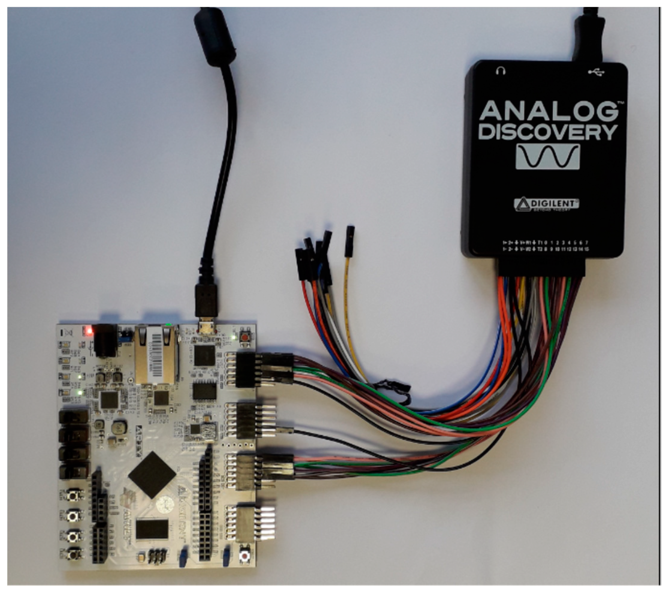
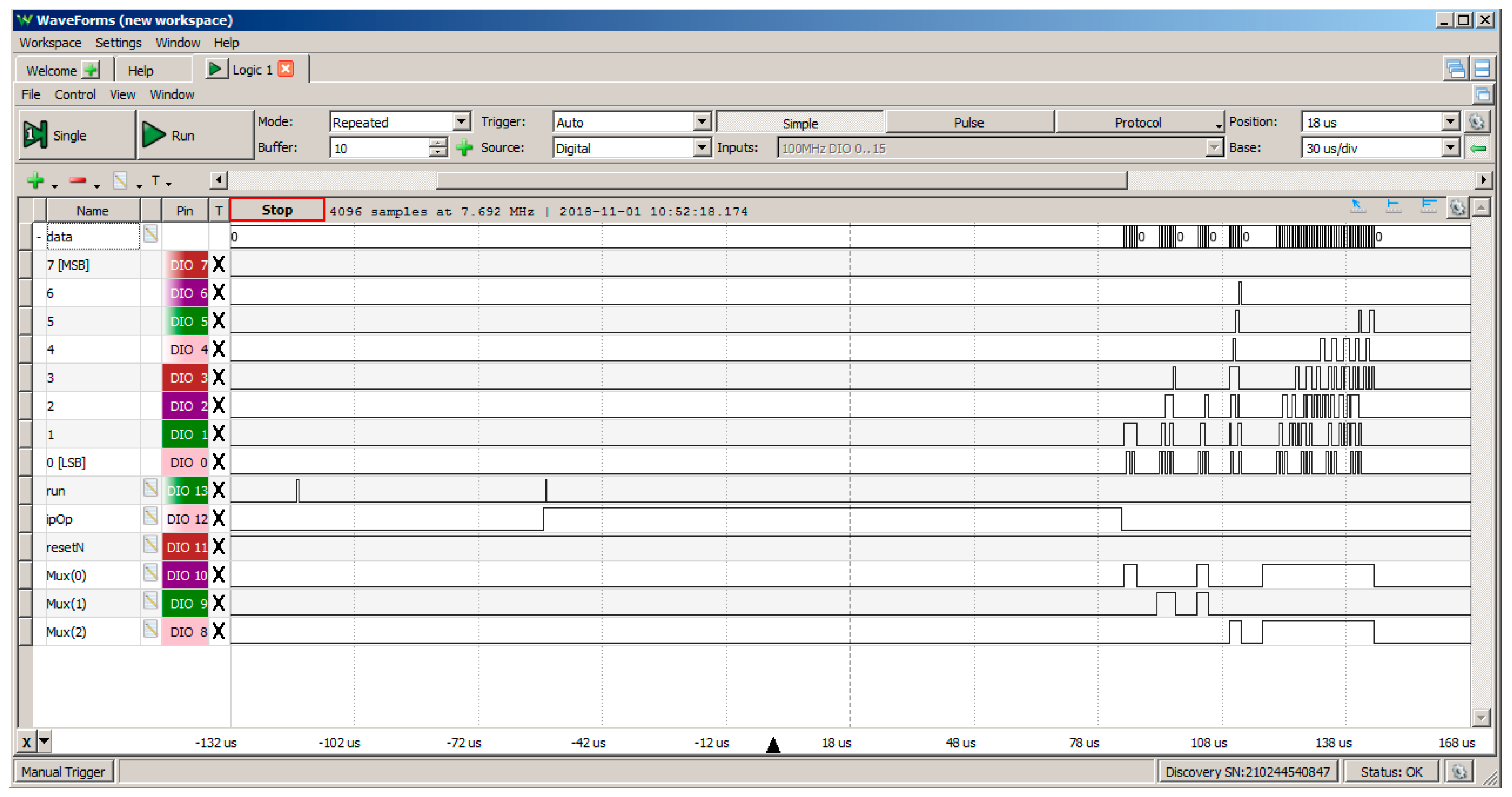
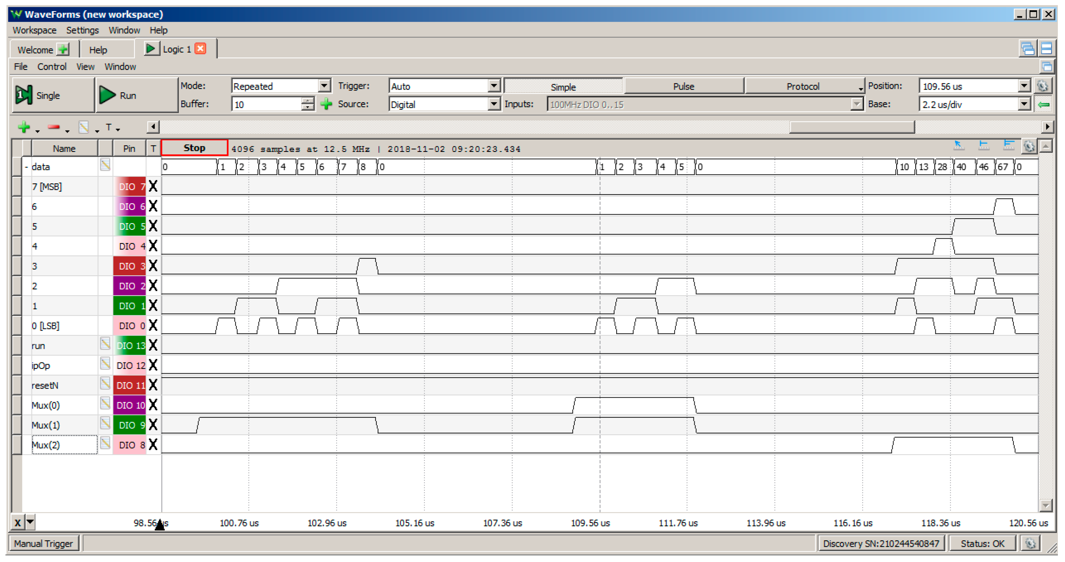
5.5. Hardware Test Set-Up

Design analysis was in the main performed using simulation to determine correct functionality and signal timing considering the initial design description prior to synthesis (behavioral simulation), the synthesized design (post-synthesis simulation), and the implemented design (post-implementation simulation). This is a typical simulation approach that is supported by the FPGA simulator for verifying the design operation at different steps in the design process. Given that the design is intended to be used as a block within a larger digital system, the simulation results would give an appropriate level of estimating the signal timing and the circuit power consumption.
In addition to the simulation study, the design was also implemented within the FPGA and signal monitored using the development board connectors (the PmodTM (peripheral module) connectors) using a logic analyzer and oscilloscope. This test arrangement is shown in Figure 12.
To generate the top-level design module input signals, a built-in tester circuit was developed and incorporated into the FPGA. This was a form of a built-in self-test (BIST) [30] circuit that generated the control signals identified in Figure 5 and allowed the internal array address and data signals to be accessed. The tester circuit was set-up to continuously repeat the sequence in Figure 5 rather than run just once and so did not require any user set input control signals to operate. With the number of address and data bits required (40 address bits and 40 data bits) for the five arrays that exceeded the number of PmodTM connections available, these signals were multiplexed to eight address and eight data bits within the built-in tester and the multiplexor control signals were output for identifying the array being accessed. The control signals were also accessible on the PmodTM connectors for test purposes.
Figure 13 shows a simplified schematic view of the elaborated VHDL code, where I0 is the top-level design module and I1 is the built-in tester module.
The hardware test arrangement was useful to verify that the signals were generated correctly and matched the logic levels expected during normal design operation. However, it was necessary to reduce the speed of operation to account for non-ideal electrical parasitic effects that caused ringing of the signal. In this specific set-up, speed of operation of the circuit when monitoring the signals using the logic analyzer and oscilloscope was not deemed important, so the 100 MHz clock was internally divided within the built-in tester circuit to 2 MHz in the study. However, further analysis could determine how fast the signals could change if the PmodTM connector was required to connect external memory for larger data sets.
Figure 14 shows the logic analyzer test set-up with the Artix-7 FPGA Development Board (bottom left) and the Digilent® Analog Discovery “USB Oscilloscope and Logic Analyzer” (top right) [31]. The 16 digital inputs for the logic analyzer function were available for use and a GND (ground, 0) connection was required to monitor the test circuit outputs. Internal control signals (ClockTop, ipOp, run, and resetN) were also available for monitoring in this arrangement.
The Digilent® Waveforms software [32] was utilized to control the test hardware and view the results. Figure 15 shows the logic analyzer output in Waveforms. Here, one complete cycle of the test process is shown, where the calculations are initially performed and the array outputs then read. The logic level values obtained in this physical prototype test agreed with the results from the simulation study. The data values are shown as a combined integer number value (data, top) and the values of the individual bits (7 down to 0).
The run signal (a 0-1-0 pulse) initiates the computation that is selected by the ipOp signal at the start of the cycle. The data readout on the 8-bit data bus can be seen towards the end of the cycle as both a bus value and individual bit values.
Figure 16 shows the data readout operation towards the end of the cycle. The data output identifies the values for array A (nine values), array B (six values), and the inner product result array (six values) as identified in Section 5.2.

5.6. Design Implementation Considerations

This case study design has presented one example implementation of the combined inner and outer product algorithm. The study focused on creating a custom hardware only design implementation rather than developing the algorithm in software to run on a suitable processor architecture. The approach taken to create the hardware design was to map the algorithm operations in software to a hardware equivalence. The hardware design was created using two main modules:
  • The computation module.
  • The control module. The control module was required to receive control signals from an external system and transform these to internal control signals for the computation module.
The computation module itself was modelled as two separate sub-modules as this was based on the underlying structure of the problem that was to efficiently access data from memory for running a computation on data held in specific memory locations:
  • The memory module.
  • The algorithm module.
For a specific application, the memory module would be used for storing input data, intermediate results data, and final (output) data. For this design, the physical memory used was internal to the FPGA using distributed memory within the LUTs given the size of the data set, the availability of hardware resources within the FPGA, and the synthesis tool that automatically determined what hardware resources were to be used. The memory was modelled using VHDL arrays where the input data arrays held constant values and the intermediate and output data arrays held variables. In a different scenario, the memory modelling in VHDL might be different. For example, explicitly targeting internal BRAM cells and external memory attached to the FPGA pins. Such an approach would resemble a standard processor architecture with different levels of memory. The internal latches, flip-flops, distributed RAM, and BRAM cells within the FPGA would map to cache memory internal to the processor and external memory to attached memory devices as depicted in Figure 3.
The designer would have design choices when considering the algorithm module. One approach would be to use a standard processor architecture that would be software programmed and mapped to hardware resources within the FPGA. Depending on the device, the processor may be an embedded core (a so-called hard core) or may be an IP block that can be instantiated in a design and synthesized into the available FPGA logic (a so-called soft core). For example, in Xilinx® FPGAs, then the MicroBlaze 32-bit RISC (reduced instruction set computer) CPU can be instantiated into a custom design. It is also possible to have, if the hardware resources are sufficient, instantiated multiple soft cores within the FPGA. This would allow for a multi-processor solution and on-chip processor-to-processor communications with parallel processing. A second approach would be to develop a custom architecture solution that maps the algorithm and memory modules to the user requirements, giving a choice to implement sequential or parallel (concurrent) operations. This provides a high level of flexibility for the designer, but requires a different design approach, thinking in terms of hardware rather than software operations. A third approach would be to create a hardware-software co-design incorporating custom architecture hardware and standard processor architectures working concurrently.
A final consideration in implementation would to be identify example processor architectures and target hardware used in machine and deep learning applications, where their benefits and limitations for specific applications could be assessed. For example, in software processor applications, then the CPU is used for tensor computations where a GPU (graphics processing unit) is not available. GPUs have architectures and software programming capabilities that are better than a CPU for applications, such as gaming, where high-speed data processing and parallel computing operations are required. An example GPU is the Nvidia® Tensor Core [33].

6. Conclusions

In this paper, the design and simulation of a hardware block to implement a combined inner and outer product was introduced and elaborated. This work was considered in the context of developing embedded digital signal processing algorithms that can effectively and efficiently process complex data sets. The FPGA was used as the target hardware and the product algorithm developed as VHDL modules. The algorithm was initially evaluated using C and Python code before translation to a hardware description in VHDL. The paper commenced with a discussion into tensors and the need for effective and efficient memory access to control memory access times and the cost associated with such memory access operations. To develop the ideas, the FPGA hardware implementation developed was an example design that paralleled an initial software algorithm (C and Python coding) used for algorithm development. The design was evaluated in simulation and hardware implementation issues were discussed.

Author Contributions

The authors contributed equally to the work undertaken as a co-design effort. Co-design is not just giving tasks to scholars in separate yet complementary disciplines. It is an ongoing attempt to communicate ideas across disciplines and a desire to achieve a common goal. This type of research not only helps both disciplines but it gives definitive proof of how that collaboration achieves greater results, and mentors students and other colleagues to do the same. The case study design was a hardware implementation by Ian Grout using the FPGA of the algorithm developed by Lenore Mullin. Both authors contributed equally to the background discussions and the writing of the paper.

Funding

This research received no external funding.

Conflicts of Interest

The authors declare no conflict of interest.

References

  1. Earley, S. Analytics, Machine Learning, and the Internet of Things. IT Prof. 2015, 17, 10–13. [Google Scholar] [CrossRef]
  2. Corneanu, C.A.; Simón, M.O.; Cohn, J.F.; Guerrero, S.E. Survey on RGB, 3D, Thermal, and Multimodal Approaches for Facial Expression Recognition: History, Trends, and Affect-Related Applications. IEEE Trans. Pattern Anal. Mach. Intell. 2016, 38, 1548–1568. [Google Scholar] [CrossRef] [PubMed] [Green Version]
  3. Xilinx®. FPGA Leadership across Multiple Process Nodes. Available online: https://www.xilinx.com/products/silicon-devices/fpga.html (accessed on 9 October 2018).
  4. Xilinx®. Homepage. Available online: https://www.xilinx.com/ (accessed on 9 October 2018).
  5. Xilinx®. Artix-7 FPGA Family. Available online: https://www.xilinx.com/products/silicon-devices/fpga/artix-7.html (accessed on 9 October 2018).
  6. Daniel Fleisch. A Student’s Guide to Vectors and Tensors; Cambridge University Press: Cambridge, UK, 2011; ISBN-10 0521171903, ISBN-13 978-0521171908. [Google Scholar]
  7. Institute of Electrical and Electronics Engineers. IEEE Std 1076-2008—IEEE Standard VHDL Language Reference Manual; IEEE: New York, NY, USA, 2009; ISBN 978-0-7381-6853-1, ISBN 978-0-7381-6854-8. [Google Scholar]
  8. Kindratenko, V.; Trancoso, P. Trends in High Performance Computing. Comput. Sci. Eng. 2011, 13, 92–95. [Google Scholar] [CrossRef]
  9. Lane, N.D.; Bhattacharya, S.; Mathur, A.; Georgiev, P.; Forlivesi, C.; Kawsar, F. Squeezing Deep Learning into Mobile and Embedded Devices. IEEE Pervasive Comput. 2017, 16, 82–88. [Google Scholar] [CrossRef]
  10. Mullin, L.; Raynolds, J. Scalable, Portable, Verifiable Kronecker Products on Multi-scale Computers. In Constraint Programming and Decision Making. Studies in Computational Intelligence; Ceberio, M., Kreinovich, V., Eds.; Springer: Cham, Switzerland, 2014; Volume 539. [Google Scholar]
  11. Gustafson, J.; Mullin, L. Tensors Come of Age: Why the AI Revolution Will Help HPC. 2017. Available online: https://www.hpcwire.com/2017/11/13/tensors-come-age-ai-revolution-will-help-hpc/ (accessed on 9 October 2018).
  12. Workshop Report: Future Directions in Tensor Based Computation and Modeling. 2009. Available online: https://www.researchgate.net/publication/270566449_Workshop_Report_Future_Directions_in_Tensor-Based_Computation_and_Modeling (accessed on 9 October 2018).
  13. Tensor Computing for Internet of Things (IoT). 2016. Available online: http://drops.dagstuhl.de/opus/volltexte/2016/6691/ (accessed on 9 October 2018).
  14. Python.org, Python. Available online: https://www.python.org/ (accessed on 9 October 2018).
  15. TensorflowTM. Available online: https://www.tensorflow.org/ (accessed on 9 October 2018).
  16. Pytorch. Available online: https://pytorch.org/ (accessed on 9 October 2018).
  17. Keras. Available online: https://en.wikipedia.org/wiki/Keras (accessed on 9 October 2018).
  18. Apache MxNet. Available online: https://mxnet.apache.org/ (accessed on 9 October 2018).
  19. Microsoft Cognitive Toolkit (MTK). Available online: https://www.microsoft.com/en-us/cognitive-toolkit/ (accessed on 9 October 2018).
  20. CAFFE: Deep Learning Framework. Available online: http://caffe.berkeleyvision.org/ (accessed on 9 October 2018).
  21. DeepLearning4J. Available online: https://deeplearning4j.org/ (accessed on 9 October 2018).
  22. Chainer. Available online: https://chainer.org/ (accessed on 9 October 2018).
  23. Google, Cloud TPU. Available online: https://cloud.google.com/tpu/ (accessed on 9 October 2018).
  24. Lenore, M.; Mullin, R. A Mathematics of Arrays. Ph.D. Thesis, Syracuse University, Syracuse, NY, USA, 1988. [Google Scholar]
  25. Mullin, L.; Raynolds, J. Conformal Computing: Algebraically connecting the hardware/software boundary using a uniform approach to high-performance computation for software and hardware. arXiv. 2018. Available online: https://arxiv.org/pdf/0803.2386.pdf (accessed on 1 November 2018).
  26. Institute of Electrical and Electronics Engineers. IEEE Std 1364™-2005 (Revision of IEEE Std 1364-2001), IEEE Standard for Verilog® Hardware Description Language; IEEE: New York, NY, USA, 2006; ISBN 0-7381-4850-4, ISBN 0-7381-4851-2. [Google Scholar]
  27. Ong, Y.S.; Grout, I.; Lewis, E.; Mohammed, W. Plastic optical fibre sensor system design using the field programmable gate array. In Selected Topics on Optical Fiber Technologies and Applications; IntechOpen: Rijeka, Croatia, 2018; pp. 125–151. ISBN 978-953-51-3813-6. [Google Scholar]
  28. Dou, Y.; Vassiliadis, S.; Kuzmanov, G.K.; Gaydadjiev, G.N. 64 bit Floating-point FPGA Matrix Multiplication. In Proceedings of the 2005 ACM/SIGDA 13th International Symposium on Field-Programmable Gate Arrays, Monterey, CA, USA, 20–22 February 2005. [Google Scholar] [CrossRef]
  29. Amira, A.; Bouridane, A.; Milligan, P. Accelerating Matrix Product on Reconfigurable Hardware for Signal Processing. In Field-Programmable Logic and Applications, Proceedings of the 11th International Conference, FPL 2001, Belfast, UK, 27–29 August 2001; Lecture Notes in Computer Science; Brebner, G., Woods, R., Eds.; Springer: Berlin/Heidelberg, Germany, 2001; pp. 101–111, ISBN 978-3-540-42499-4 (print), ISBN 978-3-540-44687-3 (online). [Google Scholar]
  30. Hurst, S.L. VLSI Testing—Digital and Mixed Analogue/Digital Techniques; The Institution of Engineering and Technology: London, UK, 1998; pp. 241–242. ISBN 0-85296-901-5. [Google Scholar]
  31. Digilent®. Analog Discovery. Available online: https://reference.digilentinc.com/reference/instrumentation/analog-discovery/start?redirect=1 (accessed on 1 November 2018).
  32. Digilent®. Waveforms. Available online: https://reference.digilentinc.com/reference/software/waveforms/waveforms-3/start (accessed on 1 November 2018).
  33. Nvidia. Nvidia Tensor Cores. Available online: https://www.nvidia.com/en-us/data-center/tensorcore/ (accessed on 1 November 2018).
Figure 1. Programmable/configurable device choices for implementing digital signal processing operations in hardware and software.
Electronics 07 00320 g001
Figure 2. Algorithm execution (memory access) of time vs. memory hierarchy.
Electronics 07 00320 g002
Figure 3. Availability of memory types in IoT applications.
Electronics 07 00320 g003
Figure 4. ipOpCore case study design.
Electronics 07 00320 g004
Figure 5. Computation control signal timing diagram.
Electronics 07 00320 g005
Figure 6. Simplified system block diagram.
Electronics 07 00320 g006
Figure 7. Simplified schematic view of the elaborated VHDL code.
Electronics 07 00320 g007
Figure 8. Xilinx® Artix-7 FPGA on the Digilent® Arty board identifying key components used in the experimentation.
Electronics 07 00320 g008
Figure 9. Simulation study results: Computation and results read-out.
Electronics 07 00320 g009
Figure 10. Simulation study results: Inner product.
Electronics 07 00320 g010
Figure 11. Simulation study results: Outer product (final set of results read-out only).
Electronics 07 00320 g011
Figure 12. Embedded hardware tester.
Electronics 07 00320 g012
Figure 13. Embedded hardware tester: Simplified schematic view of the elaborated VHDL code.
Electronics 07 00320 g013
Figure 14. Logic analyzer test set-up using the Digilent® Analog Discovery.
Electronics 07 00320 g014
Figure 15. Logic analyzer test results using the Digilent® Analog Discovery: Complete cycle.
Electronics 07 00320 g015
Figure 16. Logic analyzer test results using the Digilent® Analog Discovery: Data readout.
Electronics 07 00320 g016
Table 1. Tensor rank (0 to n) with an example code using Python lists.
Rank.Mathematical EntityExample Realization in Python Code
0Scalar (magnitude only)A = 1
1Vector (magnitude and direction)B = [0,1,2]
2Matrix (two dimensions)C = [[0,1,2], [3,4,5], [6,7,8]]
3Cube (three dimensions)D = [[[0,1,2], [3,4,5]], [[6,7,8], [9,10,11]]]
nn dimensions
Table 2. PLD vendors and devices [27].
VendorFPGASPLD/CPLDCompany Homepage
Xilinx®Virtex, Kintex, Artix and SpartanCoolRunner-II, XA CoolRunner-II and XC9500XLhttps://wwwxilinxcom/
Intel®Stratix, Arria, MAX, Cyclone and Enpirion---https://wwwintelcom/content/www/us/en/fpga/deviceshtml
Atmel Corporation (Microchip)AT40Kxx family FPGAATF15xx ATF25xx, ATF75xx CPLD families and ATF16xx, ATF22xx SPLD familieshttps://wwwmicrochipcom/
Lattice SemiconductorECP, MachX and iCE FPGA familiesispMACH CPLD familyhttp://wwwlatticesemicom/
MicrosemiPolarFire, IGLOO, IGLOO2, ProASIC3, Fusion and Rad-Tolerant FPGA families---https://wwwmicrosemicom/product-directory/fpga-soc/1638-fpgas
Table 3. Artix-7 FPGA resource utilization in the case study design.
ItemUseNumber Used
Package pinInput44
Output40
Design synthesis results
Post-synthesis I/OInputs23 *
Outputs40
Slice LUTsTotal used454
LUT as logic442
LUT as memory (distributed RAM)12
Slice registersTotal used217
Slice register as flip-flop217
Other logicClock buffer2
Design implementation results
Post-implementation I/OInputs23
Outputs40
Slice LUTsTotal used391
LUT as logic379
LUT as memory (distributed RAM)12
Slice registersTotal used217
Slice register as flip-flop217
Other logicClock buffer2
* Note that the number of inputs required in the design after synthesis do not include the address input bits that were always a constant logic 0 in this case study. This was due to the standard 8-bit address bus used for all input addresses and the sizes of the arrays meant that most significant bits (MSBs) of the array addresses were not required. Note also that post-implementation, the number of slice LUTs required was less than that post-synthesis.

