1. Introduction
In recent years, electrical vehicle (EV) and hybrid electrical vehicle (HEV) manufacturers have increased the capacity of their batteries in order to improve the mileages of their vehicles. As a result, rapid chargers for electric vehicles are also having their power ratings increased to match the increasing battery capacities, and for fixed chargers, bidirectional power transfer capabilities for vehicle to grid (V2G) are required. However, it is difficult to develop a bidirectional EV charger that can charge the batteries that are currently being developed with various rated voltages and rated powers. A two-quadrant charger has been studied for EV charger. It uses two active switches, is capable of bidirectional power transfer, and has a relatively simple configuration of gate driver and control circuit. However, there is a disadvantage; this system is bulky and expensive because a large current flows through the two output stage inductors [
1]. Also, a dual-buck AC/DC half bridge converter has been studied as a four-quadrant converter. By arranging two active switches in a diagonal structure, four-quadrant operation is possible, which can be used as an EV charger, but it is more expensive and its control is more complicated than the two-quadrant charger because an additional circuit is required [
2]. Therefore, series and parallel module systems that can easily extend their rated powers and operate the bidirectional power transfer are being researched.
Series and parallel module systems often use isolated DC/DC converters. The most common isolated DC/DC converter is the full bridge converter [
3,
4]. This converter performs the operation of the zero voltage switching (ZVS) by using a phase shift PWM technique using the leakage inductance of the transformer; thus, a highly efficient system can be developed even at high switching frequencies. Also, the secondary diode can be configured as a switch to enable bidirectional power transfer [
5,
6,
7].
However, the disadvantage of the full bridge converters used in higher rated current systems is that it is difficult to reduce the sizes of high current transformers and output stage inductors. In addition, high voltage spikes are produced in the secondary switching device because there is no loop in the leakage inductor of the transformer to release the energy stored during the discharge. In order to address this, additional circuits, such as the active clamp, are necessary [
8,
9,
10].
A topology that enables bidirectional power control without the use of an output stage inductor and active clamp circuit is the DAB converter.
Which most commonly uses the single-phase shift (SPS) technique, which shifts the phase of the primary and secondary voltages. In addition, various switching techniques are currently being developed, such as the extended phase shift (EPS) technique, which can increase the number of ZVS areas using only switching techniques and dual phase shift (DPS) technology that can improve the transient state. However, since the DAB converter has an output capacitor behind the switch module, the ripple current flowing through the switching device greatly affects the ripple current of the output capacitor [
11,
12,
13]. This is why many systems use a design that increases the allowable ripple current of capacitors on the low voltage side by having multiple capacitors in parallel, but the DAB converters are difficult to apply to low voltage and high current systems because the current ripple of the capacitor is larger than the battery charge current. [
14,
15,
16,
17]. Also, the isolated bidirectional DAB generally has high power density and fast control performance. However, the use of a large number of switches and high frequency transformers makes system costly and the control method is relatively complicated. In addition, the DAB converter has another advantage of being able to significantly reduce the weight, though it is more expensive than the full bridge converter [
18].
The CFFB converter is a topology that can improve this current ripple of the capacitor. The CFFB converter has an output capacitor behind the inductor filter, which reduces the current ripple of the capacitor more than the conventional DAB converters, and can also be smaller than the conventional full-bridge converter by interleaved operation. However, it is difficult to reduce the circulating current, because doing so requires an active clamp circuit that can discharge the stored energy of the transformer of the leakage inductor during the discharge, as in the bidirectional full-bridge converter. When an active clamp circuit is added to the CFFB converter, the circuit configuration of the DAB converter appears as part of the entire circuit, and the DAB converter PWM technique is available for the CFFB converter. Accordingly, this allows for a wide ZVS range, which is the advantage of the DAB [
19,
20,
21], and a low circulating current as well as a converter configuration with low current ripple characteristics of the output capacitor, which are advantages of the CFFB converter [
22,
23]. In addition, since a 3-phase configuration, such as CFFB, is possible, as in a CFFB converter, it is possible to design the optimal passive element through an interleaving operation.
This paper proposes the operation technique of a 3P-CFDAB converter with the addition of an active clamp circuit to the 3-phase CFFB converter.
Section 2 compares the advantages and disadvantages of different EV charger topologies.
Section 3 analyzes the introduction of a 3P-CFDAB converter and soft switching characteristics.
Section 4 analyzes the operating characteristics of the 3P-CFDAB converter by means of mode analysis. Also, the areas of ZVS and ZVT are analyzed using the mode specific current.
Section 5 and
Section 6 give the simulation and experimental results for validation of the proposed operation techniques with the 3P-CFDAB converter;
Section 7 provides the conclusion.
2. 3P-CFDAB Converter
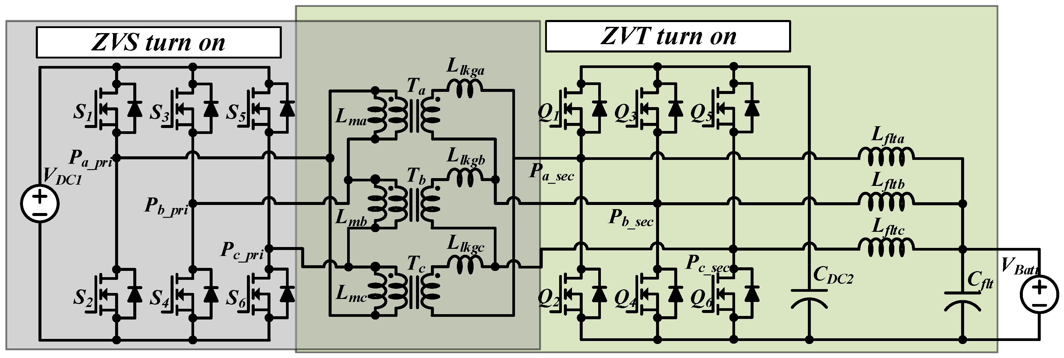
Figure 1 shows a configuration of the 3P-CFDAB converter. As shown in this figure, the primary side of the 3P-CFDAB converter consists of the same structure as the 3-phase inverter, and the secondary side consists of the 3-phase current fed converter. In addition, the primary and secondary sides are coupled with 3-phase delta-typed connection transformer. Q1, Q3, Q5, and
CDC2 consist of the active clamp circuit of the current fed full bridge converter in order to compensate for the voltage when the main switches Q2, Q4, and Q6 are turned off.
However, the 3P-CFDAB converter can be analyzed as the 3-phase DAB converter from the primary side to the active clamp circuit, and the second side can also be analyzed as a bidirectional buck-boost converter. In addition, the 3P-CFDAB converter has different soft switching characteristics on the primary and secondary sides because of the structure, as shown in
Figure 1. In the case of the primary side switching devices, there is a voltage source in front of the half bridge, as shown in
Figure 2a, and alternating current flows through the node with the same frequency as the switching frequency. Because of this alternating current, a negative current flow through the diode in the lower switch when turning off the upper switch, at this time, can then operate ZVS by turning on the switch. In the secondary side switching devices, the alternating current is received through the half bridge node as shown in
Figure 2b, and the direct current is output. In each device, current flows by the difference between alternating current and direct current; as a result, the ZVT operation interval occurs [
24].
Analysis of the soft switching conditions (shown in
Figure 2) requires consideration of how alternating current is generated on the primary and secondary side and why direct current occurs in the output stage on the secondary side. However, the 3P-CFDAB converter can see many inflection points present in the phase current and switch current within one gate pulse interval, as shown in
Figure 2, because the phase current of phase A is affected by the current of the phase A transformer and C transformer by the delta-typed connection transformer, and the current of the phase A transformer is affected by the line-to-line voltage of the phase A and B.
Therefore, the modeling of the switching states of the primary and secondary sides, and the current and voltage of the transformer of the each phase are required in order to analyze the phase current of the primary side phase A.
For the analysis of the primary and secondary phase currents, the current modeling was described in
Section 3; and in
Section 4, the areas of ZVS and ZVT are analyzed using phase current and switching device current.
3. Mode Analysis of the 3P-CFDAB Converter
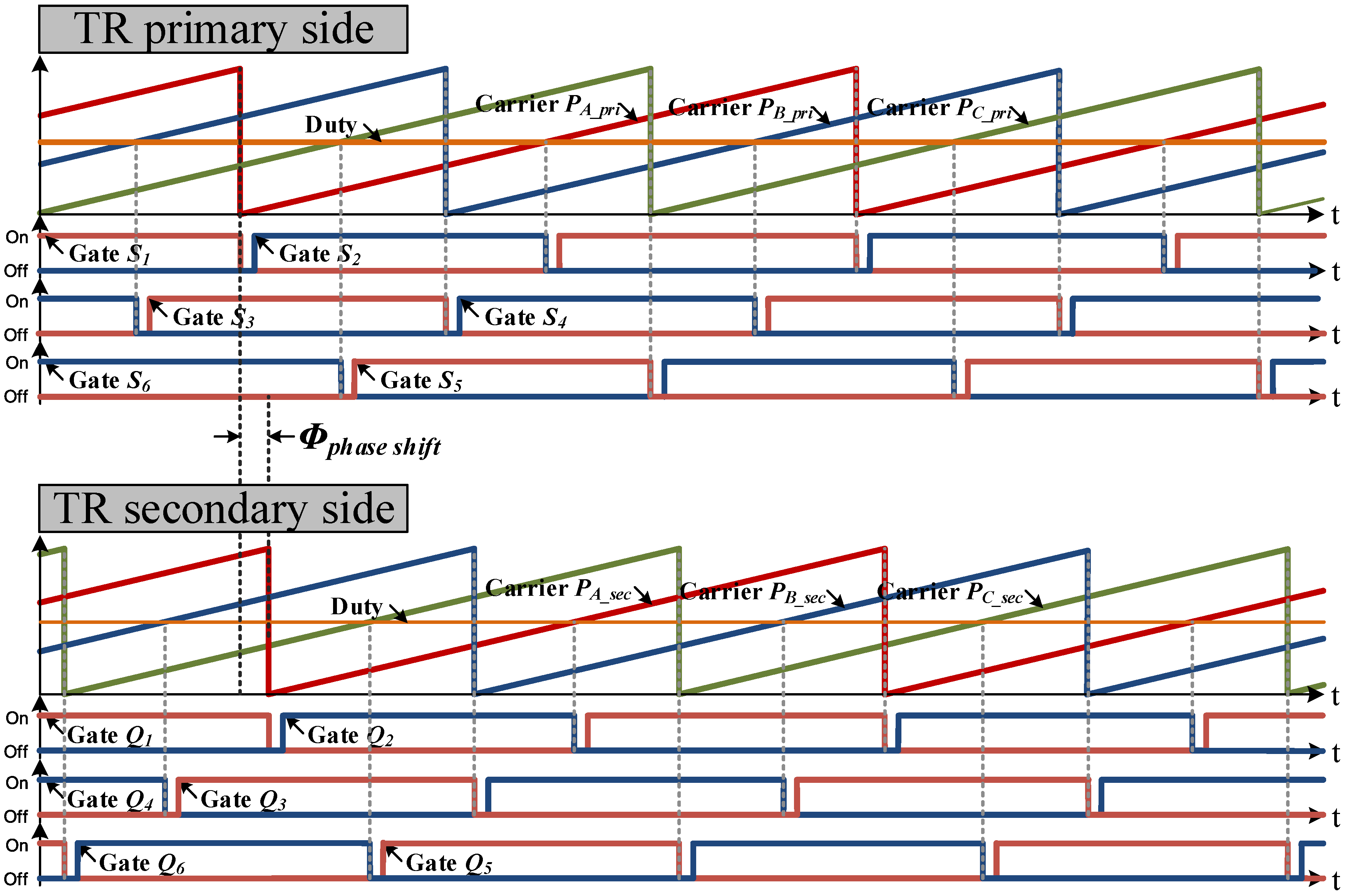
Figure 3 shows modulation technique and switching operation of the 3P-CFDAB converter. As shown in
Figure 3, the switching devices of the primary side are modulated by three carriers with 120 degree phase shifting. The switching devices of the secondary side are modulated by three carriers which are shifted by
ϕ in the primary side carriers, and duty ratio. Also, switching devices of each phase perform a complementary operation with an interval that does not turn on the upper and lower switches during the dead-time.
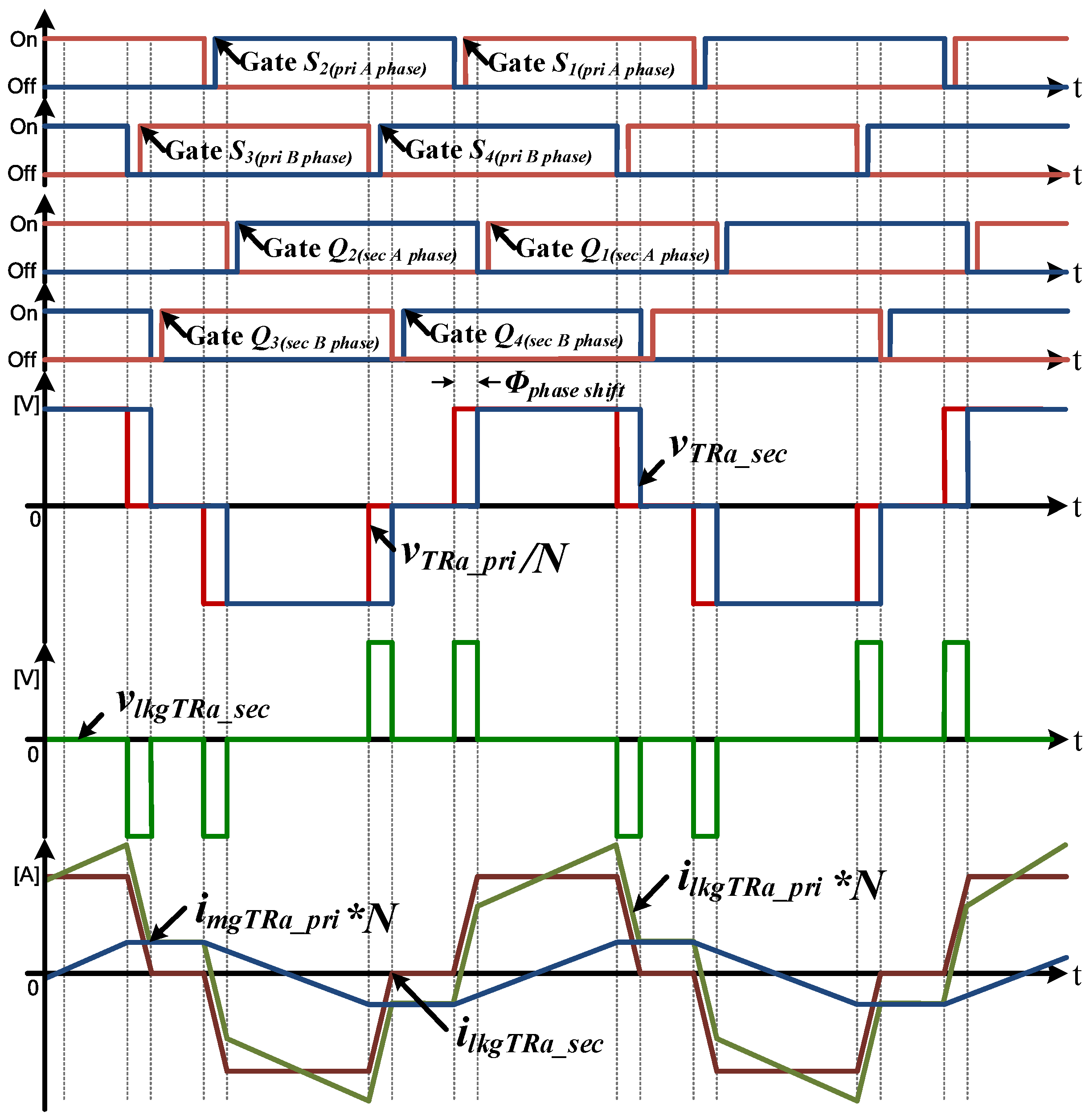
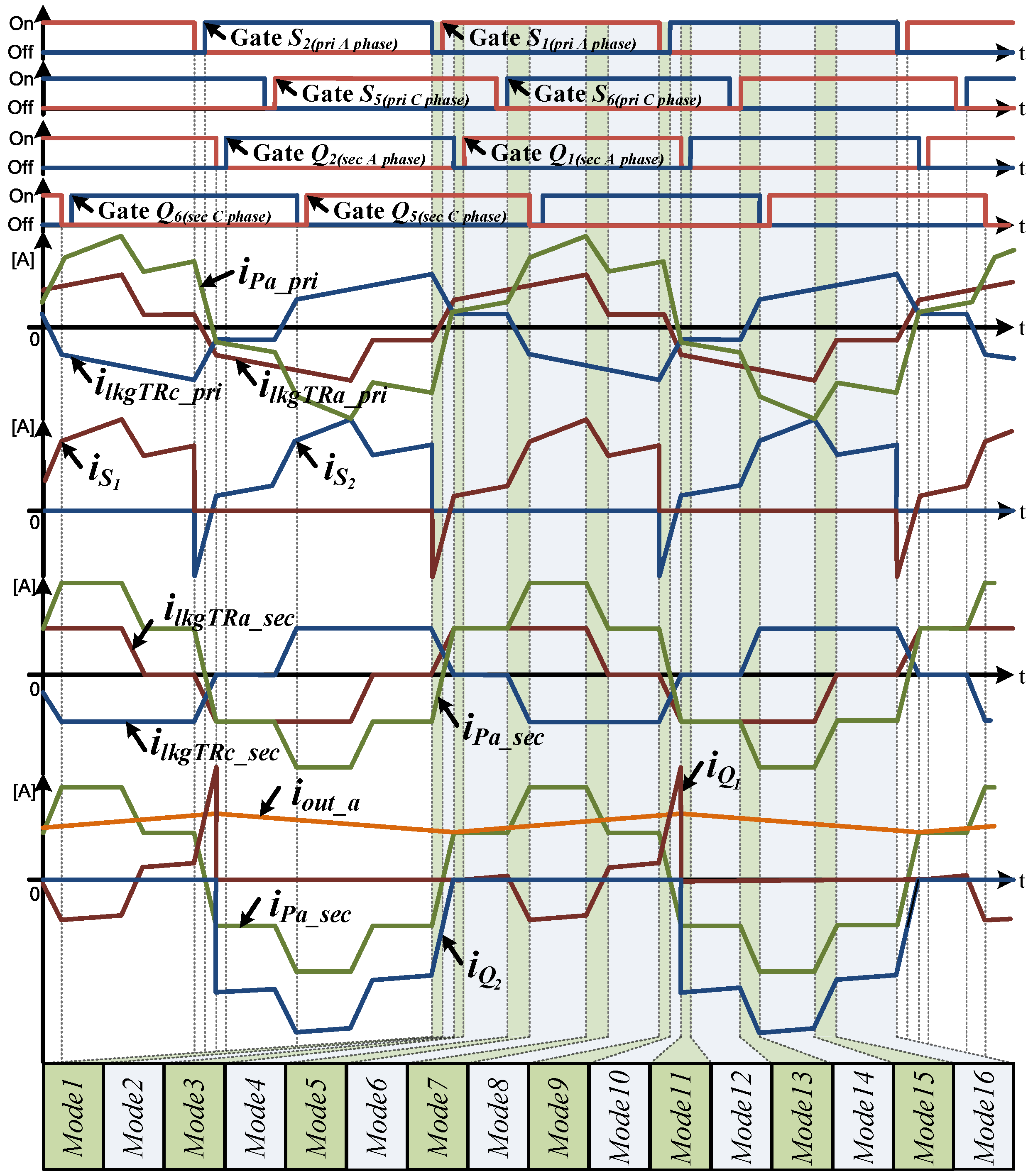
Figure 4 and
Figure 5 show the mode analysis and waveforms of the 3P-CFDAB converter based on primary and secondary side phase currents by applying the phase shift technique. The 3P-CFDAB converter consists of a primary and secondary line voltage applied to the transformer, as shown in
Figure 1 The phase current
iPa_sec consists of both
ilkgTRa_sec and
ilkgTRc_sec which are the currents of the secondary side phase A and C transformer.
As a result, the primary side voltage of Ta is affected by the switching action of phase A and phase B, which results in 3-level voltage. Also vTRa_pri, which is the line to line voltage of the primary side phase A transfer, is affected by both phase A and B switching signals such as gate S1, S2, S3, and S4, and vTRa_sec, which is the line to line voltage of the secondary side, is affected by phase shift technique.
If the phase is shifted with the same ratio on the primary and secondary sides, as shown in
Figure 4, there will be a voltage difference between the primary and the secondary sides, and this voltage difference is applied to the leakage inductor of the transformer. As a result, there will be a voltage difference between
vTRa_pri/N and
vTRa_sec, and this voltage difference (
vlkgTRa_sec) is applied to the leakage inductor of the transformer. If the voltage of the secondary DC-link (
VDC2) and the primary DC -link voltage (
VDC1) divided by the turn ratio are the same,
vlkgTRa_sec will be zero voltage because there is no difference in voltage between the primary and the secondary sides. Then, the leakage inductor is charged with voltage only in the area where the phase shift occurs, and
ilkgTRa_sec, which is the current of secondary side transformer, will increase at the area.
The current of magnetizing inductor (
imgTRa_pri) is influenced by the voltage between
vTRa_pri and appears as shown in
Figure 4, and the primary side current (
ilkgTRa_pri) combined with the transformer current is proportional to the turn ratio. The phase current of phase A (
iPa_pri), shown in
Figure 5, is applied to the difference current between
ilkgTRa_pri and
ilkgTRc_pri. The currents of primary side switching device such as
iS1 and
iS2 are affected by the
iPa_pri which is the phase current of phase A, and they are chopped by off signals of each switch. The currents of secondary side switching devices such as
iQ1 and
iQ2 are affected by both
iPa_sec, which is the phase current of phase A, and the current of output inductor (
iout_a), and these currents are applied by the current difference between
iPa_sec and
iout_a, and they are chopped by off signals of each switch.
Thus, the 16 operation modes appear based on the point of inflection of the phase current and the dead-time of the switching devices. The time for each mode is shown in
Table 1, the transformer phase A and B current of the secondary side for each section are shown in
Table 2 and
Table 3. Also, the phase A and C current of the primary side magnetizing inductor are shown in
Table 4 and
Table 5.
3.1. Mode 1
Figure 6 shows the current flow at the start of the Mode 1. The secondary phase current
iPa_sec will flow due to the difference between the current of the phase A transformer and phase C transformer. In mode 1, when the current phase A transformer increases and becomes equal to the current of the phase C transformer, the current
iPa_sec is zero. The current flow when the secondary phase current reaches zero is shown in
Figure 7.
To calculate the phase current of the primary side in Mode 1, first the voltage of the leakage inductor must be obtained. The voltage
vlkgTRa_sec across the leakage inductor can be calculated as the difference between the voltage of the primary side transformer divided by turn ratio and the voltage on the secondary side transformer. Since the secondary voltage is 0 [V], the voltage of the primary side transformer divided by turn ratio appears in the leakage inductor. Also, the
VDC2 appears to be inversely proportional to the turn ratio of the
VDC1, so voltage on leakage inductors can be expressed as follows.
Depending on (1), the current flowing through the leakage inductor is calculated as (2). These leakage inductors are indicated as the currents of the secondary side transformer, since they are based on the voltage on the secondary side of the transformer.
The current of the primary side transformer is calculated as the sum of the secondary current and the magnetizing inductor current. The current of the magnetizing inductor is significantly affected by the voltage on the primary side transformer, so it can be calculated as
The phase A current of the primary side transformer can be calculated as shown in (4) as the sum of (2) and (3).
The phase C current of the secondary side transformer with phase shifted by 120 degrees appears with the same direction like the phase A current of the secondary side transformer, calculated as follows.
Likewise, the current of the phase C magnetizing inductor with phase shifted by 120 degrees can be calculated like the current of the phase A magnetizing inductor in Mode 7, and it is expressed as follows.
The phase C current of the primary side transformer is calculated by adding the magnetizing inductor current and the secondary side current which is divided by turn ratio. It is expressed as follows.
The phase current of the primary side phase A is calculated by difference with the current of the phase A transformer and the current of the phase C transformer. It can be expressed as follows.
3.2. Mode 2
Mode 2 is the range during which the S1 switch on the primary-side is turned on, and the capacitor of S1 is completely discharged. In addition, the phase current and switch current show the same characteristics as those in Mode 1.
3.3. Mode 3
Mode 3 is the dead-time range from when Q1 is turned until Q2 is turned off. When Mode 3 is started, Q2 is turned off, the parasitic capacitance is charged, and the voltage multiplied by the turn ratio of the primary side, the voltage of the transformer becomes equal to the secondary side voltage of the transformer. Thus, the current slope of the leakage inductor becomes zero, and the primary transformer current rises with the magnetizing inductor current slope. In this case, the primary and secondary transformer currents can be calculated as shown in equation (9) via the equation in
Table 2 and
Table 4 for Mode 3.
3.4. Mode 4
Mode 4 is the range while the Q2 on the secondary side is turned on. The capacitor of Q2 is completely discharged, and the phase current and switch current all have the same characteristics as those in Mode 3.
3.5. Mode 5
Mode 5 is the range in which the phase currents of the primary and secondary sides are varied by current of Tc. In this range, the phase currents of the primary and secondary sides rise because of the fall of the current of Tc.
3.6. Mode 6
In Mode 6, the current of the secondary side is constant as the slope of the phase C transformer of the secondary side becomes zero. At the end of Mode 6, the magnetizing inductor current is the maximum value. So the primary transformer current and the phase current also show the maximum value. The primary and secondary phase current are obtained using the equation in
Table 2 and
Table 4 for Mode 3, and the peak value can be obtained as shown in equation (10) by substituting the time in
Table 1.
3.7. Mode 7
In Mode 7, the switch S4 in the primary side phase B is turned off and the line-to-line voltage of the primary side phase A and B goes down to zero. As a result, a potential difference between the voltage applied to the primary side and the secondary side is generated in the negative direction. In this section, both the primary phase current and the secondary phase current have a negative slope because of the fall of the secondary-side transformer current. In this case, the primary and secondary transformer currents are shown in (11).
3.8. Mode 8
In Mode 8, switch Q4 in the secondary side phase B is turned off, and the line-to-line voltage of the secondary side phase A and B also becomes zero, and the voltage difference between the primary and secondary sides of the transformer becomes zero. At this time, the current flowing through the secondary side leakage inductor becomes zero, and the primary side leakage inductor current generates a circulating current because of the magnetizing inductor current.
3.9. Mode 9
Mode 9 is the period in which the phase transition starts and the dead time of the primary switch is maintained. When Mode 9 is started and S1 is turned off, the parasitic capacitance of S2 is discharged, the parasitic capacitance of S1 is charged, and the transformer voltage of the primary side phase A becomes the DC-link voltage by the parasitic capacitor voltage of S1. After Mode 9, S2 is turned on. In order to turn on the ZVS of S2, the primary side phase current must maintain a positive value until Mode 9 ends. The primary side phase current that affects this is shown in (12).
3.10. Mode 10
Mode 10 is the end of the dead time on the primary side phase A, when the capacitor of S2 is completely discharged and the phase current and switch current have the same characteristics as in Mode 9. After Mode 10, Q1 is turned off. For Q2’s ZVT turn-on, the secondary phase current must be less than the output inductor current. The current at the secondary side in Mode 10 is shown in (13).
3.11. Mode 11
Mode 11 is the dead time interval on the secondary side phase A. When Mode 11 is initiated, the Q1 switch current, which was sufficiently positive in Mode 10, is turned off, reversing the current in the direction of the diode in Q2. As a result, the parasitic capacitor of Q2 is discharged.
3.12. Mode 12
Mode 12 is the range during which the Q2 on the secondary side is turned on, and ZVT turns on when the switch current of Q2 flows in the negative direction. The Q2 switch current will appear the same as in Mode 11.
3.13. Mode 13
Mode 13 is similar to Mode 5, and the phase currents of the primary and secondary sides are varied by the current of the phase C transformer. In this range, the phase C transformer current rises and the primary and secondary phase currents have a falling slope.
3.14. Mode 14
Mode 14 has characteristics similar to those of Mode 6, in which the phase current of the secondary side becomes constant, while the current of the secondary side phase C transformer slope becomes zero. The minimum phase current at this time can be obtained as shown in (10).
3.15. Mode 15
Mode 15 is similar to Mode 7. In Mode 15 the switch S3 of the primary side phase B is turned off, so the line-to-line voltage of the primary side phase A and B drops to zero. Accordingly, the voltage is applied to both the primary and the secondary sides in the positive direction, and the phase A transformer current rises.
3.16. Mode 16
Mode 16 is similar to Mode 8 in that the switch Q3 of the secondary side phase B is turned off and the line-to-line voltage of the secondary side phase A and B also becomes zero, indicating that the difference between the primary and the secondary side voltage of the transformer is zero. At this time, the current flowing through the secondary side transformer leakage inductor becomes zero, and the primary side leakage inductor current generates a circulating current because of the magnetizing inductor current.
4. Soft Switching Analysis
The ZVS characteristics of the primary side switching devices can be found in Modes 1–2 and 9–10. The primary side phase current
iPa_pri is the same as
iS1, which is the primary side switching device current. If the time t of (1) can be more than the dead time, then S1 can be ZVS turn on in Mode 2. The time
tZVS_S1 in which (1) maintains a negative value can be obtained as follows.
ϕ in
Figure 4 means phase shift angle. As in equation (14),
tZVS_S1 appears to be inversely proportional to the switching frequency and proportional to the phase shift angle. However, in (14), since the output current is different when the phase shift angle is changed, it is necessary to adjust it to a formula representing the same output current for phase value and
Llkg.
Figure 8 shows the relationship between the phase A transformer and the output power of the phase A inductor. As shown in
Figure 8, the output power of the phase A transformer is represented by the product of the voltage and the current on the secondary side and of the transformer, and as a waveform with twice the frequency of the switching frequency.
The output power of the phase A inductor can be obtained by multiplying the phase A inductor current and the battery voltage, and except for the parasitic components, the inductor output power and transformer output power appear the same. This can be calculated as in (15) by ensuring that the product of the current integration value and the voltage of the secondary side transformer from Modes 3 to 10 are the same as the inductor output power:
Calculation of the average value of the output current by using (15) can be made as follows.
Equation (16) shows that the average value of the inductor output current is inversely proportional to the switching frequency, leakage inductance, and battery voltage, and increases proportionally to the voltage and phase of the secondary side. Also, if the quadratic formula is used to calculate (16) for the phase, it appears as shown in (17).
It is possible to obtain the time of the ZVS under the same output current conditions by substituting (17) for (14), which can be expressed as (18).
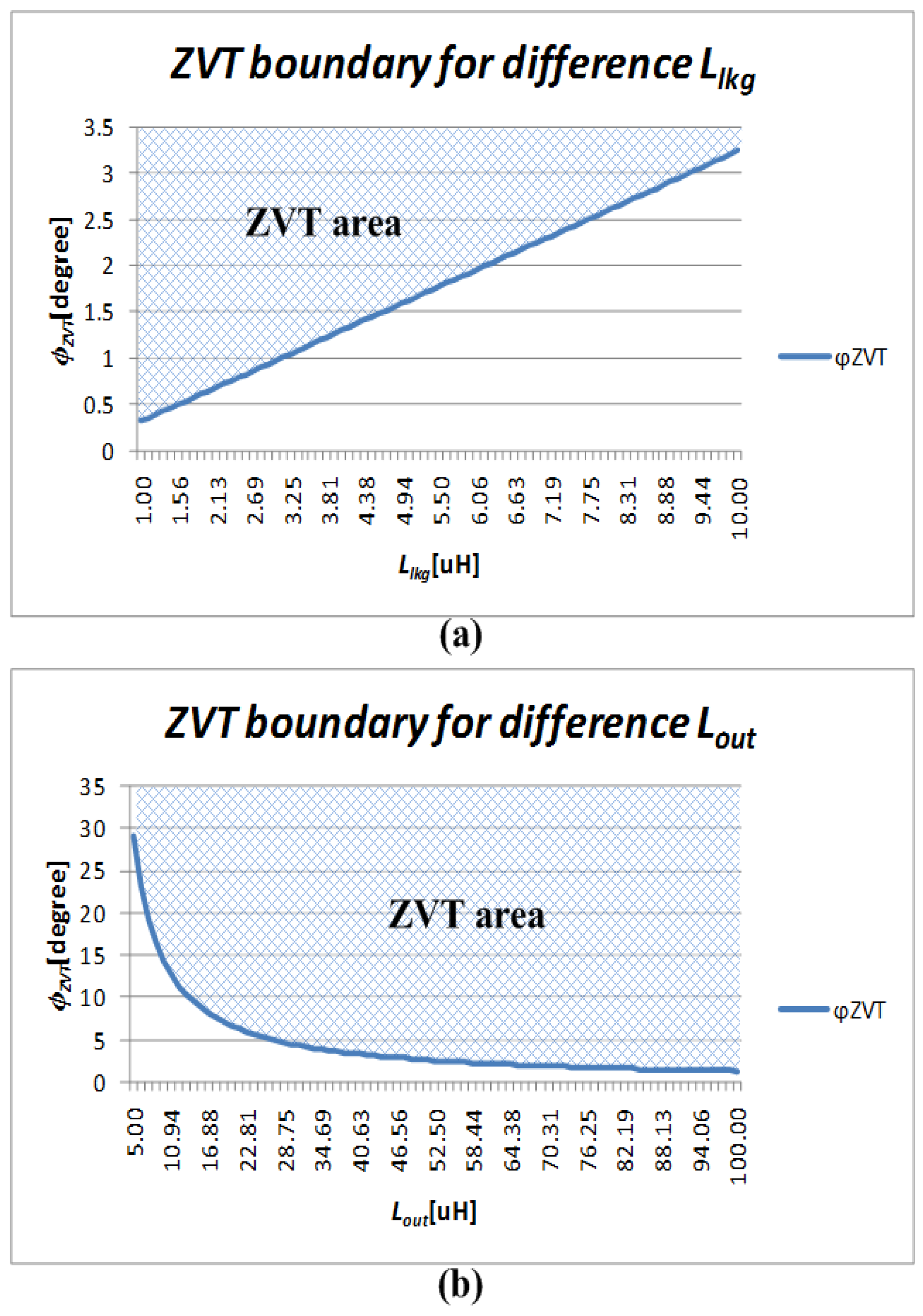
Depending on Equation (18), the ZVS areas of the primary side of the 3P-CFDAB converter is changed by leakage inductance and by magnetizing inductance of the primary side transformer. In addition, it can be seen that a primary side switching device can turn on ZVS when the dead time is less than the time of (18).
Figure 9 shows the area of the ZVS depending on the variability in the leakage and magnetizing inductance. The ZVS turn on will appear when a dead time less than that in the graph in
Figure 9 is applied. As shown in
Figure 9a, the larger the leakage inductor is, the longer the ZVS time is, and the smaller the magnetizing inductance is, the relatively longer the ZVS time is. In addition, it can be seen that the ZVS time does not vary significantly after the magnetizing inductance has increased by a certain amount, as shown in
Figure 9b As shown in
Figure 9a, the ZVS time is increased proportionally to the value of leakage inductance, however, if the leakage inductance increases, the output current decreases in an inversely proportional manner. Therefore, the leakage inductance should be selected by taking into account the maximum output current and the ZVS time.
The maximum value of the system output current is calculated as follows.
For secondary side switching devices, the upper and lower switching devices fill different roles. The lower devices act as a power transfer. The upper switch allows the lower switch to turn on ZVT after the lower switch is turned off and the current flows via the leakage inductor. For this, the current of the secondary side upper switch should be positive at the end of Mode 10. Additionally, after Mode 10 is finished, this current will flow in the negative direction to the lower switch, creating an area for making ZVT turn on. At the end of Mode 10, the current of the upper switch appears as shown in (20).
The phase in which
iQ1 has a positive current in Mode 10 can be obtained as follows.
Figure 10 shows the area of the ZVT according to variations in the leakage inductance and output inductor. As shown in
Figure 10, the ZVT area of the secondary side decreases as the leakage inductance increases, and the larger the output inductor is, the wider the area is. However, for the primary side switching devices, ZVT areas become wider as the leakage inductance increases. Therefore, for ZVS and ZVT soft switching, the leakage inductance should be selected appropriately according to the switching frequency, battery rated voltage and current, and the dead times of the switching devices. The leakage inductance of the transformer to achieve the ZVS can be obtained as shown in Equation (22), using the Equation (18).
5. Simulation
In order to verify the principle and feasibility of the proposed topology and switching method, the following simulation has been developed using the PSIM 9.1.4 software program.
Table 6 shows the simulation parameters for the 10 [kW] CF-TPDAB converter. The switching frequency selected is 120 [kHz] in order to obtain a 120 [%] power margin for output power. The leakage inductance of 7 [μH] and the magnetizing inductance of 1 [mH] were selected for the turn on operations of ZVS and ZVT. The turn ratio was chosen as 3.5:1 for a 0.5 duty ratio based on battery voltage and DC-link voltage on the primary side.
Figure 11 shows the proposed control block diagram of the 3P-CFDAB converter applied to simulation and experimental. This consists of the voltage controller for the clamp capacitor and the current controller for controlling the current of battery. The reference value of the clamp capacitor voltage is calculated by the DC voltage of the primary side and turn ration of transformer. And then, the PWM is implemented by using the output of the PI controller. The controller for CC-CV control consists of two blocks. It also consists of two controllers for the CC-CV control of the battery current. The CV controller generates a current reference value for CC control. And, the CC controller is output as the phase value for the PSM control.
The phase (), which is one of controller parameters, is variable to control the output current, and is changed according to the average value of the output current, taking into account static system parameters such as leakage inductance and switching frequency, as shown in Equation (10). Also, the duty cycle () is a variable that controls the VDC2 voltage to equal the VDC1 voltage multiplied by the turn ratio. Therefore, even though the battery voltage changes, the ZVS will be achieved over a wide range of the output voltage and will reduce the circulating current.
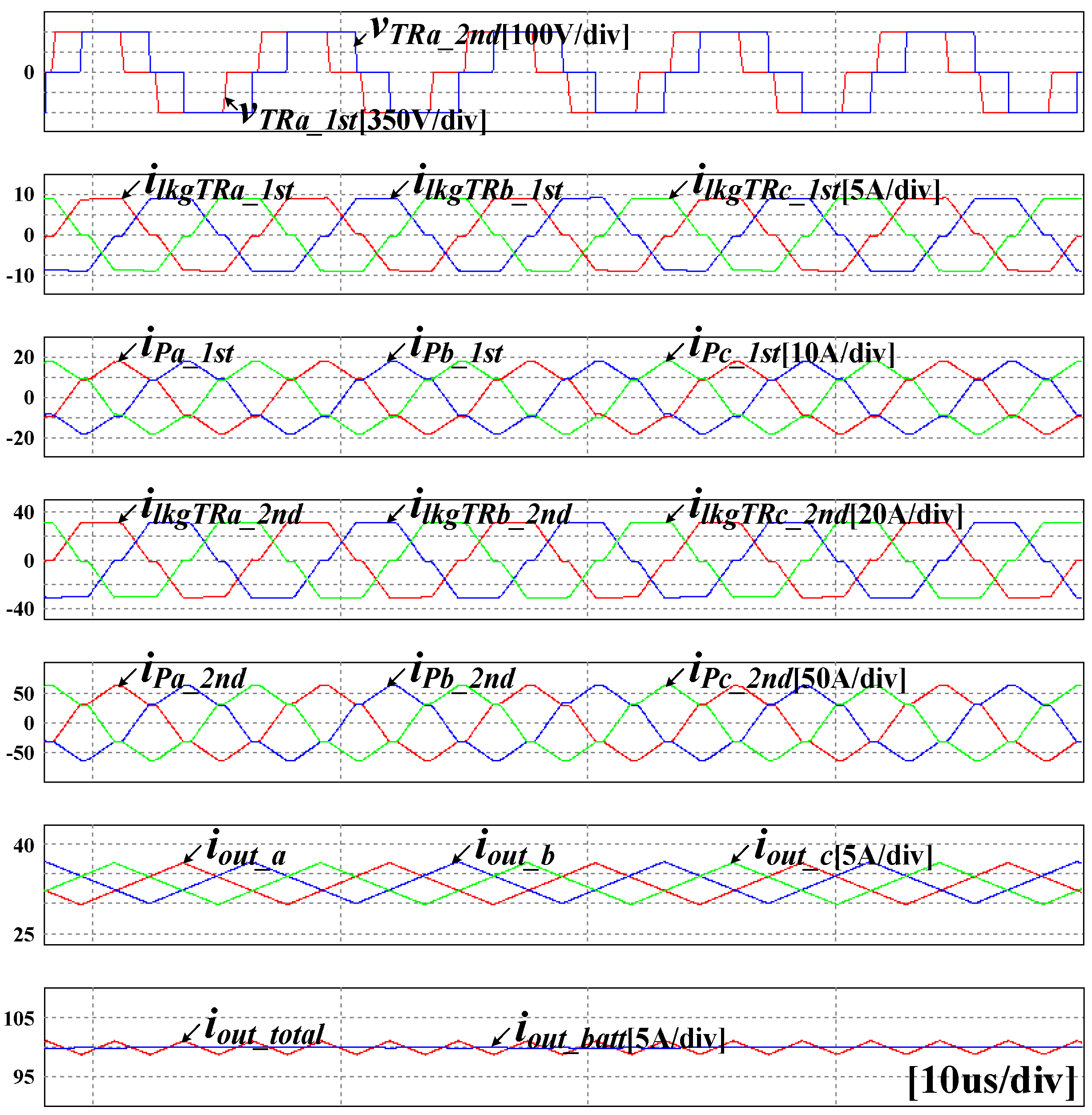
Figure 12 shows the key waveforms of the 3P-CFDAB converter. As in the simulation results, the 3P-CFDAB converter produces the primary and secondary side currents by shifting the phase of the voltage at the primary and secondary sides of the transformer. For the current of the primary side transformer, it can be seen that the magnetizing inductance current produces some inclination compared to the secondary side transformer current. The primary and secondary phase currents are generated by currents of the delta connection transformer, and the output inductor current appears as a DC current with ripple components. The three inductor currents perform an interleaving operation by a 120 degree phase shift so that the output stage current appears at frequencies three times the switching frequency.
Figure 13 shows the soft switching simulation waveforms of the primary and secondary side switching devices.
Figure 13a shows the ZVS turn on characteristics of the primary side element and performs turn on and soft switching in the areas where negative current can be seen, as mentioned in
Figure 2a The time during which ZVS is possible through (11) and
Table 6 was calculated as 0.552 μs, and the time during which the negative current of the primary side switching device could be maintained in the simulation was 0.545 μs.
Figure 13b shows the waveforms that simulate the characteristics of the ZVT for the secondary side devices. The maximum current value of the Q1 switch was calculated to be 67.6 A using (13); it was measured as 67.8 A in the simulations.
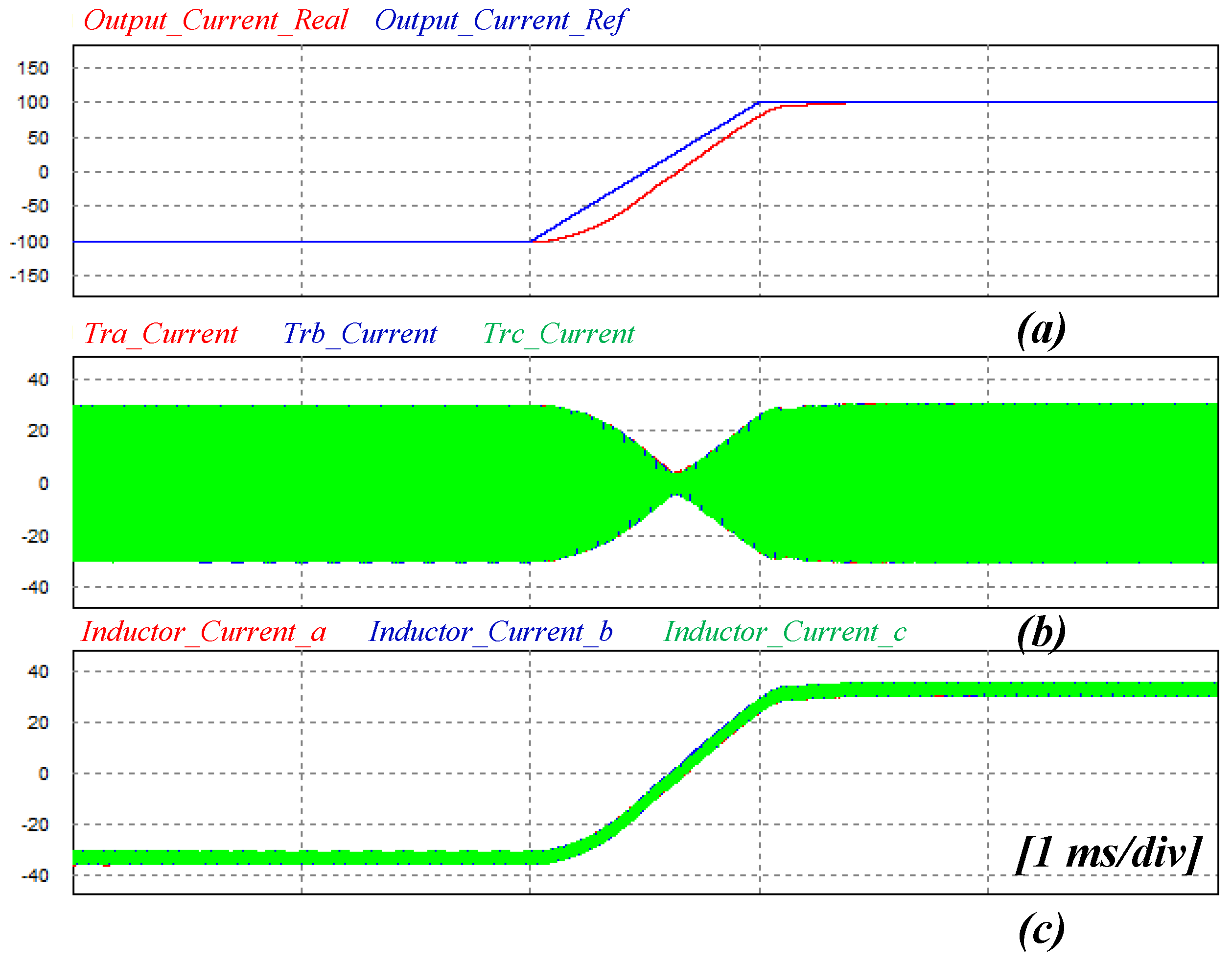
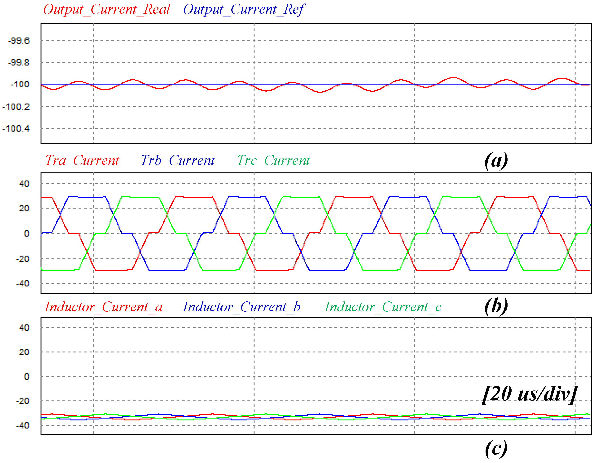
Figure 14 shows the results of the charging and discharging simulation. This shows the real output current and reference current, the current of the secondary side three phase transformer, and the current of the interleaved three phase inductor. It can be seen that the discharging operation that outputs the current of negative 100 A transfers within approximately 1 ms to the charging operation that outputs the current of positive 100 A.
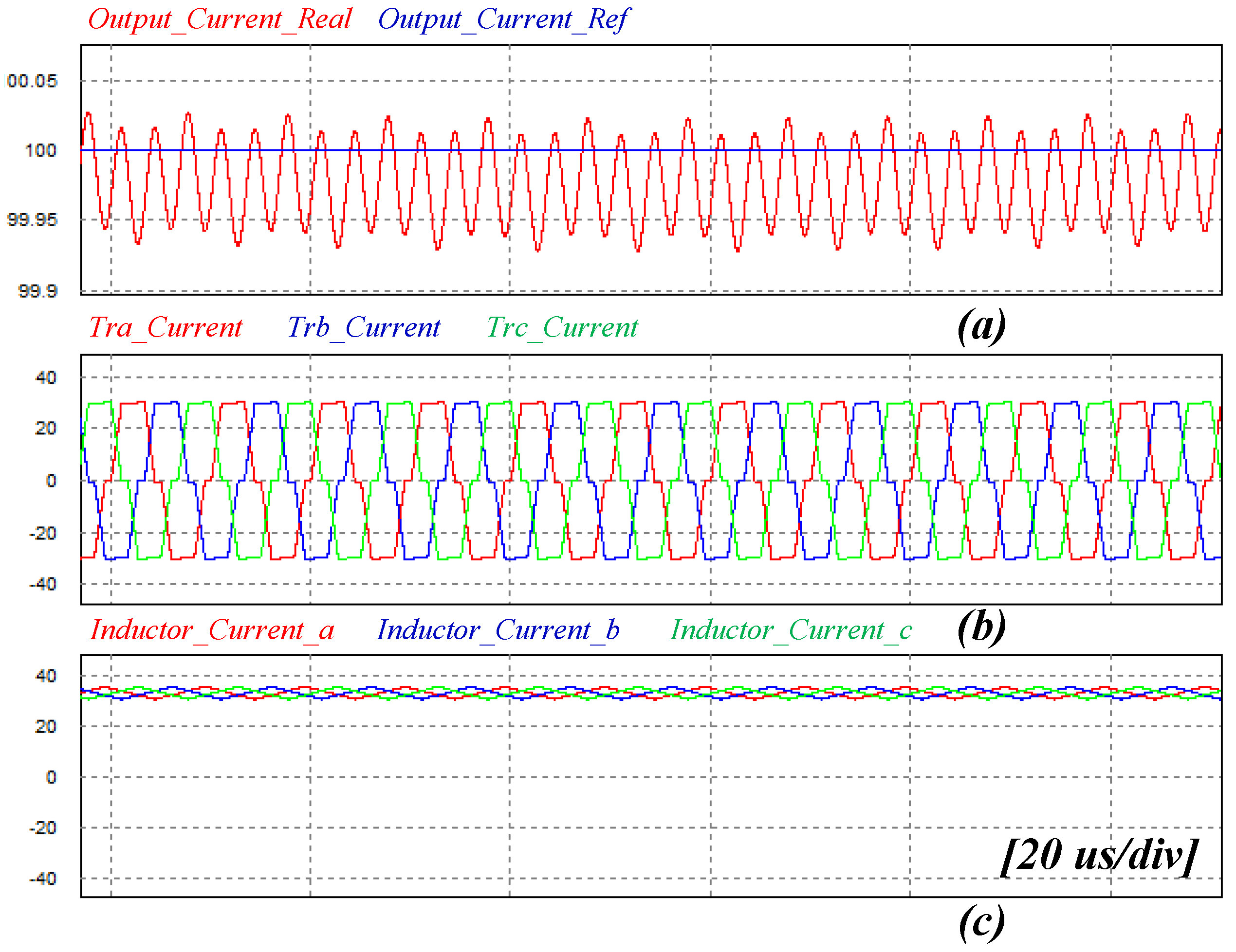
Figure 15 shows the waveforms of the simulation results during the charging operation. As shown in
Figure 15, the average current ripple of the output current is about 0.097 A during the charging operation of positive 100 A. Also, during the discharging operation of negative 100 A, the average current ripple of the output current is about 0.108 A as shown in
Figure 16. Thus, since the ripple of the output current is less than about 1 %, the system can be controlled reliably.
7. Conclusions
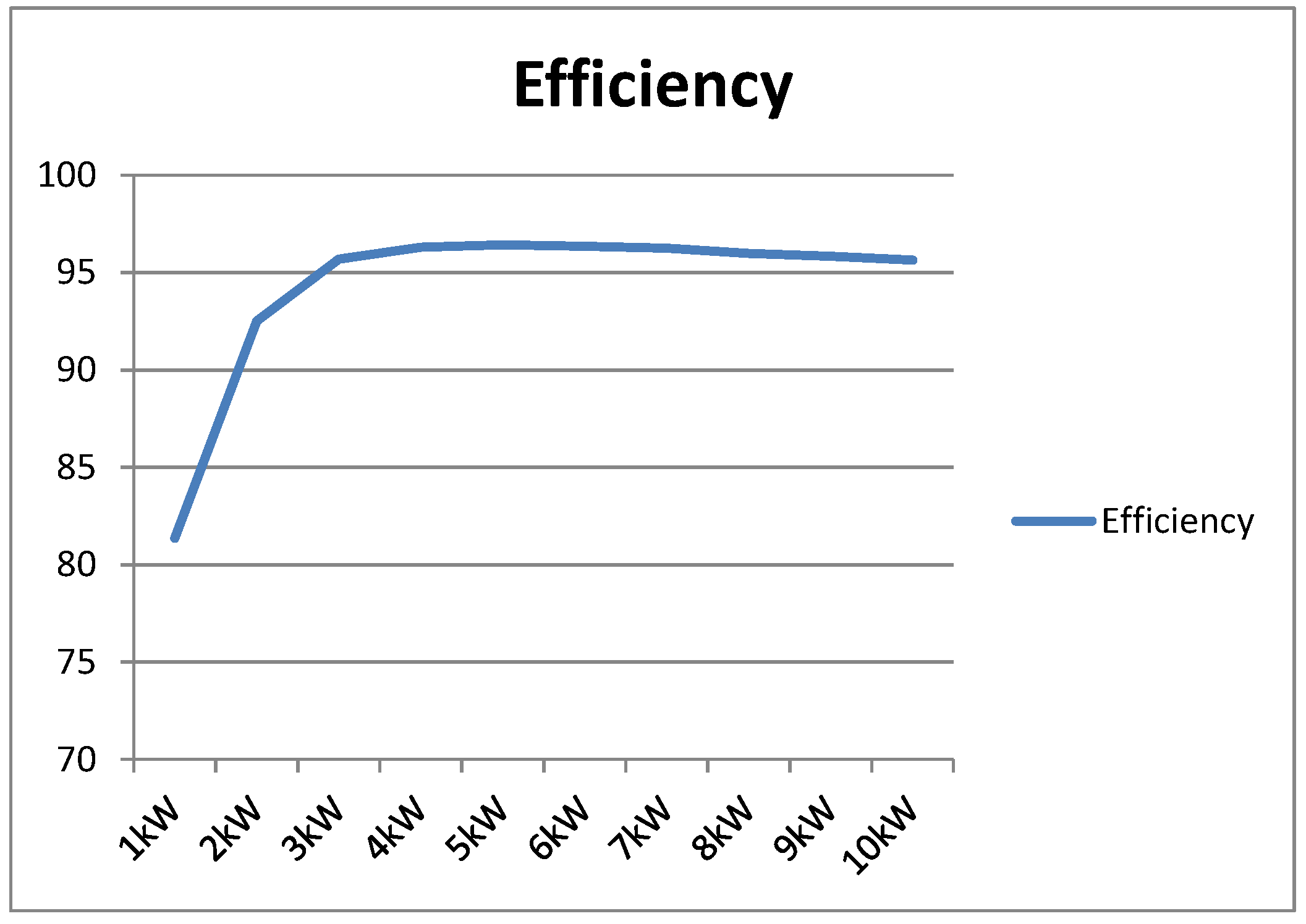
This paper proposes a power control method using the phase shift method and voltage control of a DC-link applied in a bidirectional isolated 3P-CFDAB converter. The DC-link voltage of the secondary side can be controlled stably using the phase shift method by turning the turn ratio of the transformer and reducing the reactive power of the transformer. In addition, the method of designing the leakage inductance and the transformer were analyzed in terms of the operation modes during each charge release of the 3P-CFDAB converter. As a result of the simulation and experiment, the high efficiency performance was verified by the operation of ZVS according to the wide voltage range and the load on the low voltage.
Therefore, the proposed topology and switching method of this paper have two advantages compared with the conventional DAB. First, the size of the inductive device’s inductor can be small, so that the size of output filters are reduced approximately 60%. The three parallel interleaved operations reduce the size of the passive device compared to the conventional DAB, and it is possible to design a rated current inductor of 33.4 A based on a 100 A output current. Second, a reduction in the ripple current of the capacitor. When the conventional DAB converter is operated with the SPS switching method, the current ripple of the output capacitor is approximately 61 Arms, but the current ripple of the output capacitor of the proposed topology is reduced to approximately 20 Arms under the same conditions. As a result, the rated current of the capacitor in the proposed converter can be designed to be relatively small, and the reactive power and the conduction loss are reduced compared with the conventional DAB converter. Although this paper focuses on the soft switching of the proposed topology, we will continue to study the design techniques of the inductor and transformer and the proposed topology and reactive power of the DAB converter.
