THz Rectennas and Their Design Rules


Abstract
:1. Introduction
2. Historical Notes
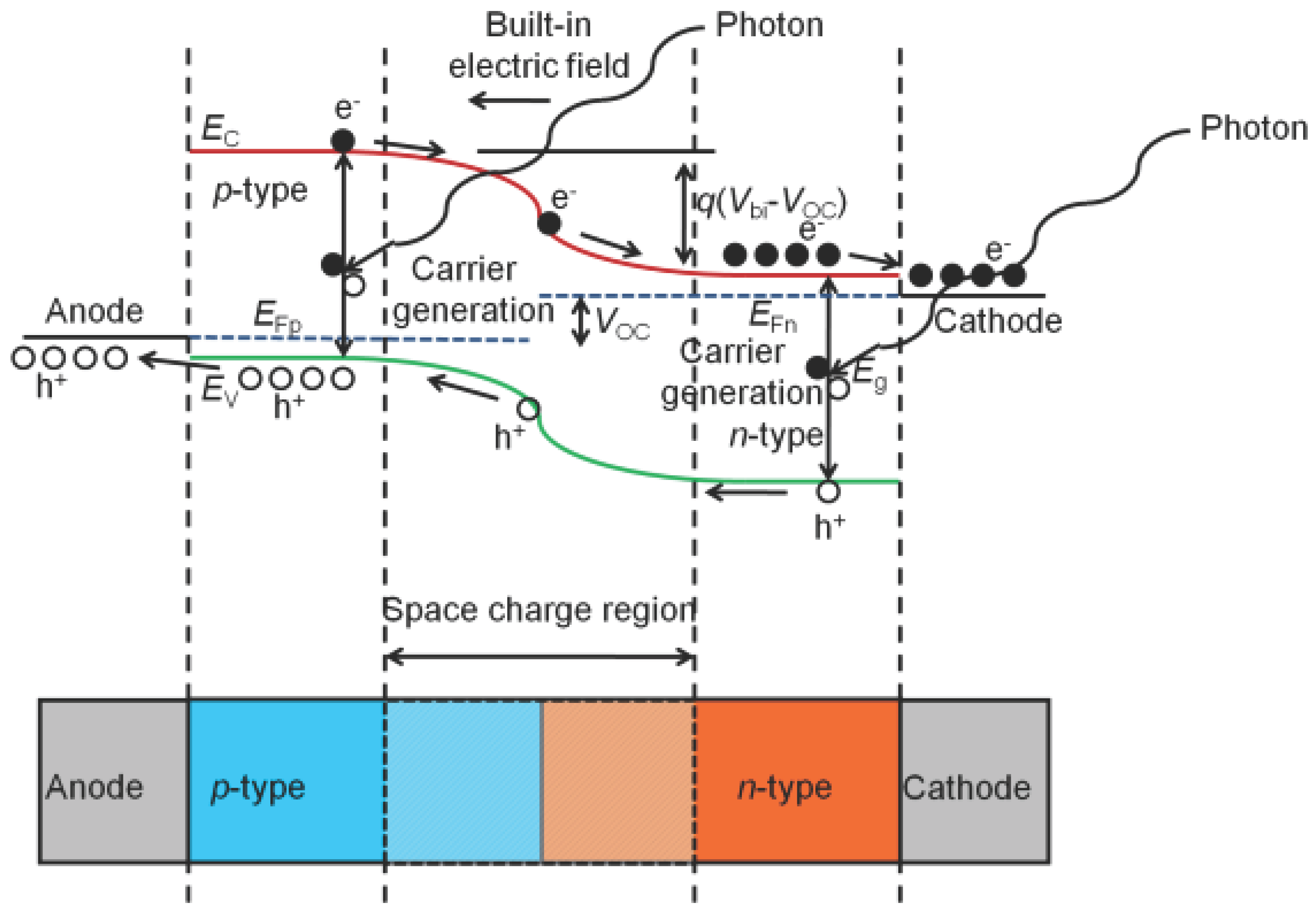
2.1. Discovery of the Photovoltaic Effect
2.2. Rectification of Electromagnetic Waves and Rectennas
2.3. Targeting Higher Frequencies
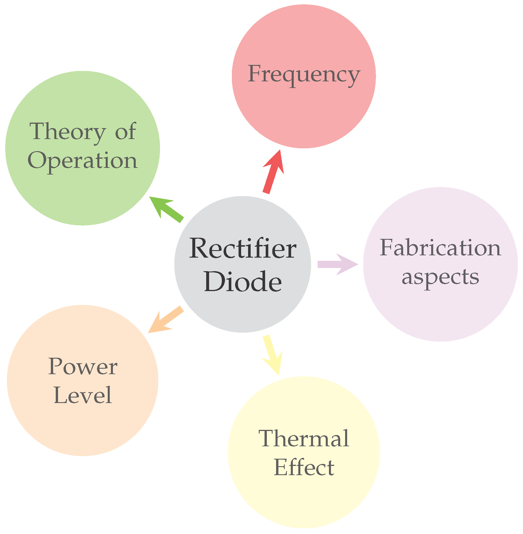
- Frequency represents the frequency of the impinging electromagnetic wave on the antenna element. Recent trials in the THz range extend over a very wide frequency range for both modeled and realized systems with frequencies starting from 1 [30], reaching the ultra violet range and exceeding 800 [31]. Strictly speaking, over this very wide range, the proposed mechanisms and expected efficiencies for implementation vary largely as will be explained later.
- The theory of operation is a controversial issue for rectennas since there are many theories of operation and so many diode types that can be structurally different based on their different theoretical framework. The difference is not only between different diode types, but also extends to having more than one theory to explain the same diode behavior. One good example is the tunneling diode as mentioned earlier in this section. A review of the widespread theoretical frameworks will be provided in Section 4.
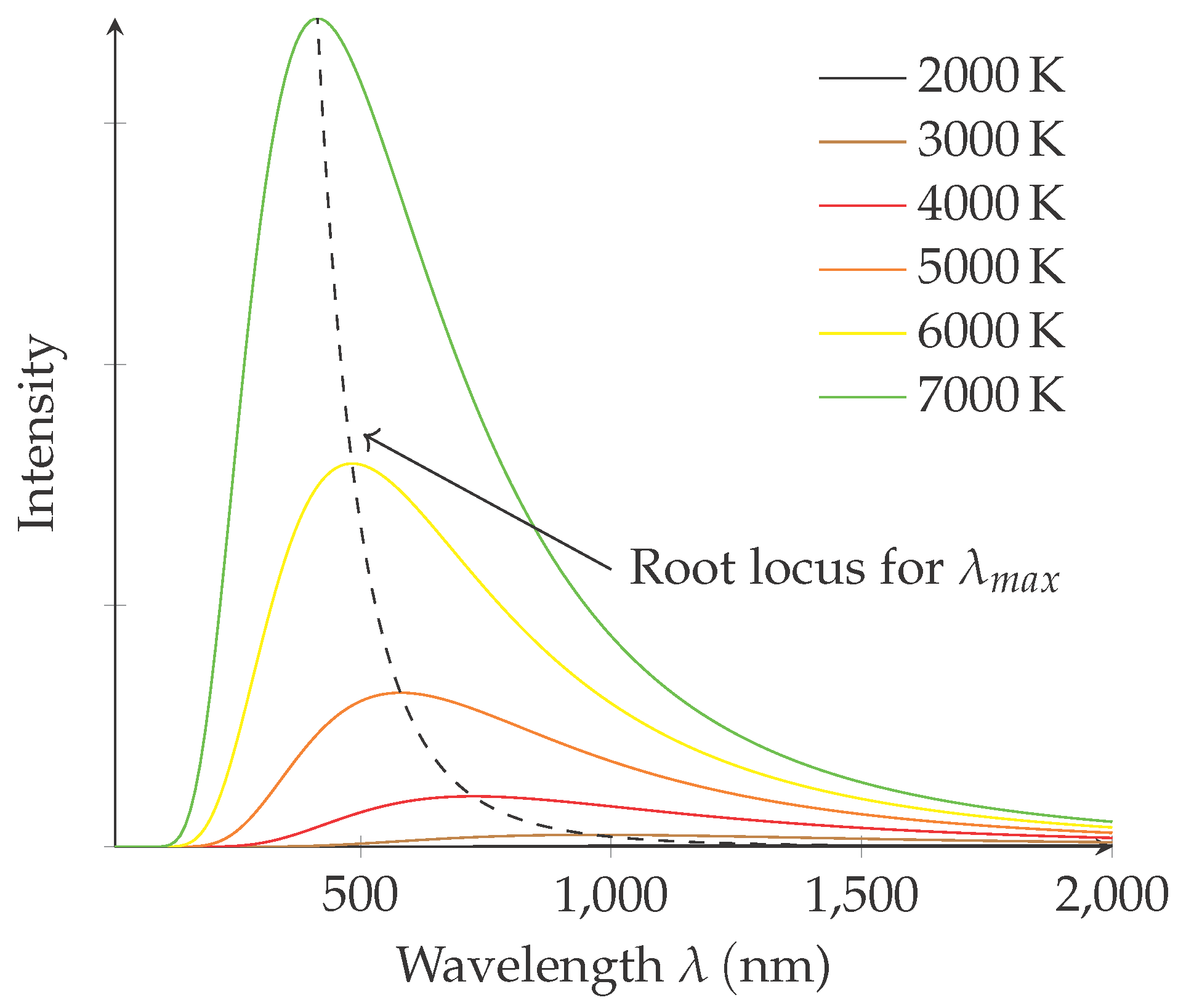
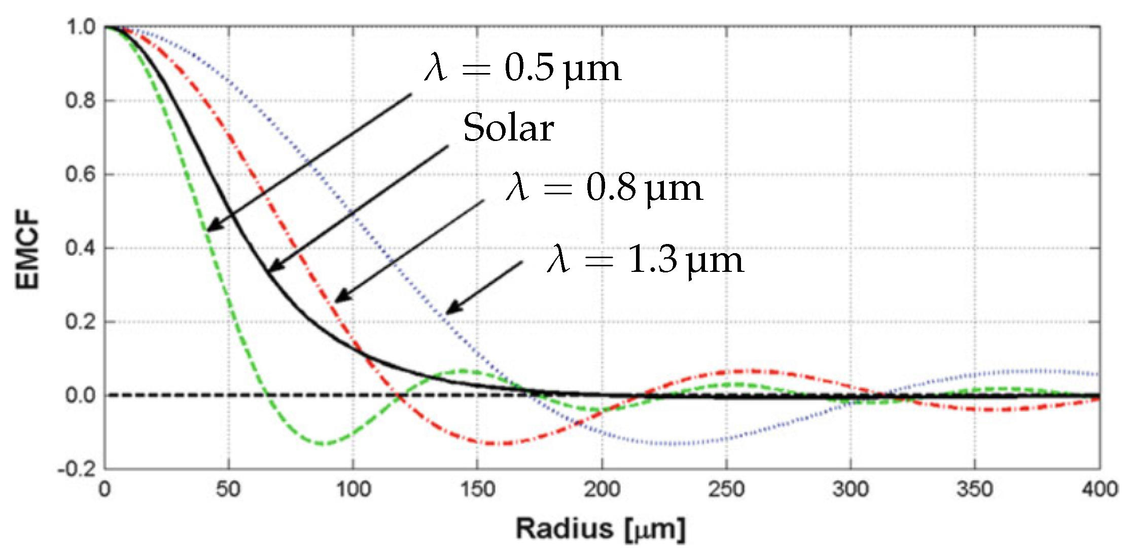
- Power level refers to the expected power level of the received signal, which can vary largely for irradiation intensities ranging from 60 for ground radiation [32] up to more than 1000 for visible light during daylight [33]. This factor can have a significant impact both on the design of the antennas and on the correct choice of the rectifying diode. Furthermore, it does not refer only to the signal input amplitude, but also largely depends on whether the signal is narrow or wide band, the coherence between different frequency components and even the distance between the source and the rectenna and how this can affect the coherence of the received wideband signal. Mashaal and Gordon [34] provide a detailed account of this issue as will be discussed later.
- Thermal effect: Although it might be argued that this factor is better considered with the theory of operation, the thermal effect is present in almost every diode application and can even take more than one form in the same application as will be seen later; the most common of which is the thermionic effect [35].
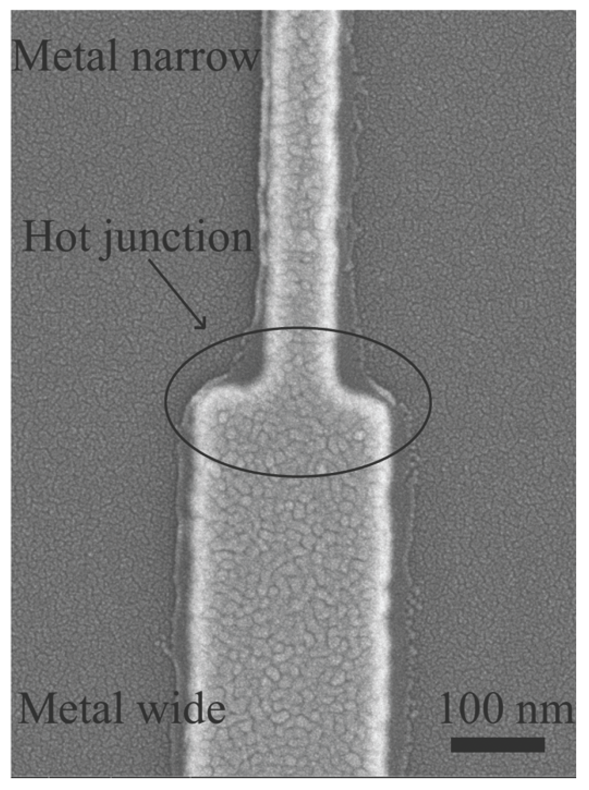
- Fabrication aspects: After a theoretical model is adopted, it would be realized using the available methods for fabricating the rectenna system at the nano-scale. This can be a challenging task, particularly, with small components whose dimensions are in the range. Although there are some promising prototypes efficiency-wise [36], which involves a vacuum clearance at the nanometer scale between the diode electrodes, realizing them in practice is a real challenge. Moreover, there are some prototypes whose behavior becomes distorted with respect to simulation because of fabrication inaccuracies as reported by Conley and Alimardini [37].
3. Frequency
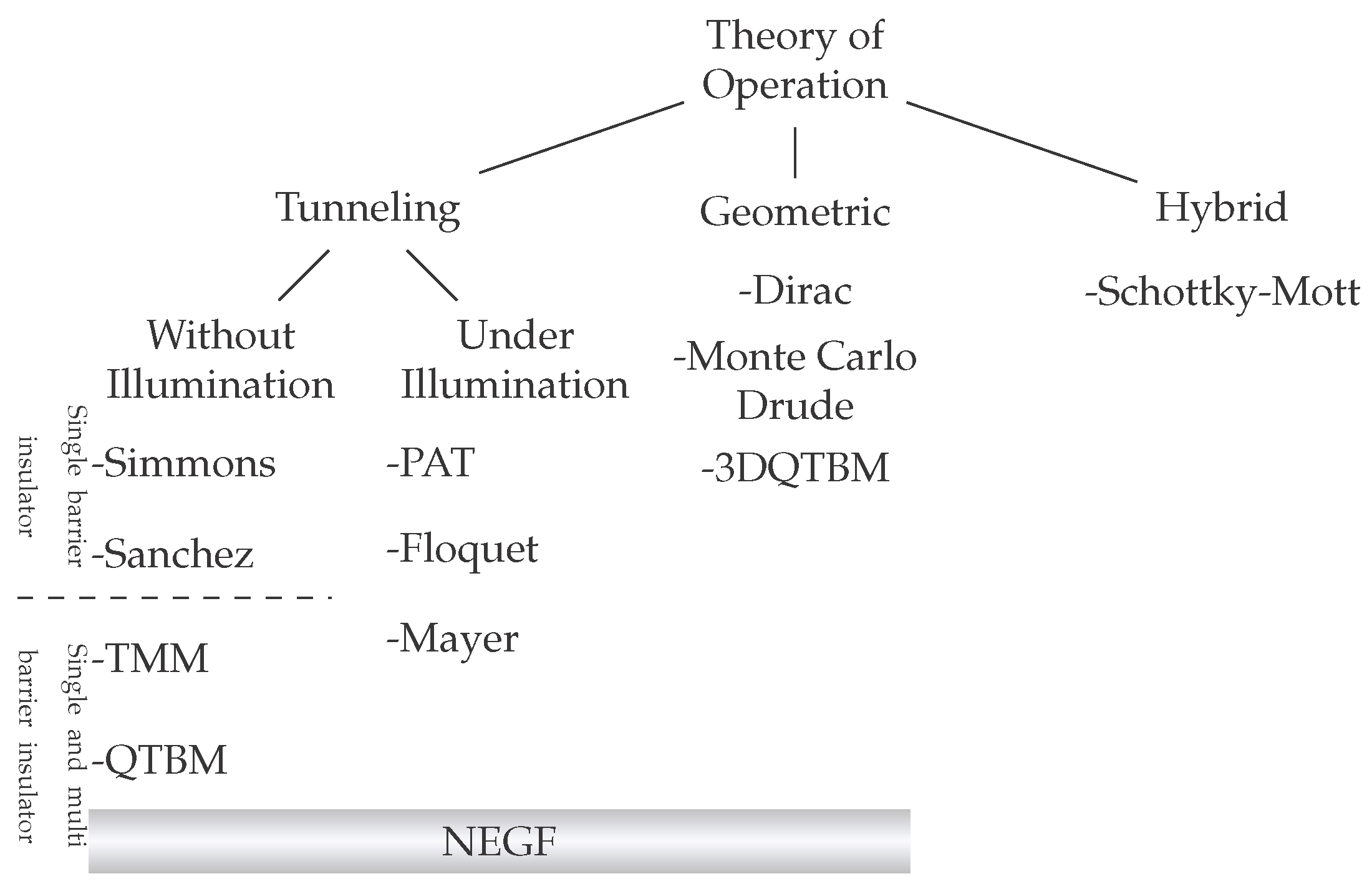
4. Theory of Operation
4.1. Tunneling
4.1.1. Without Illumination
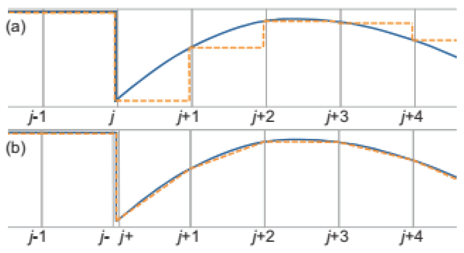
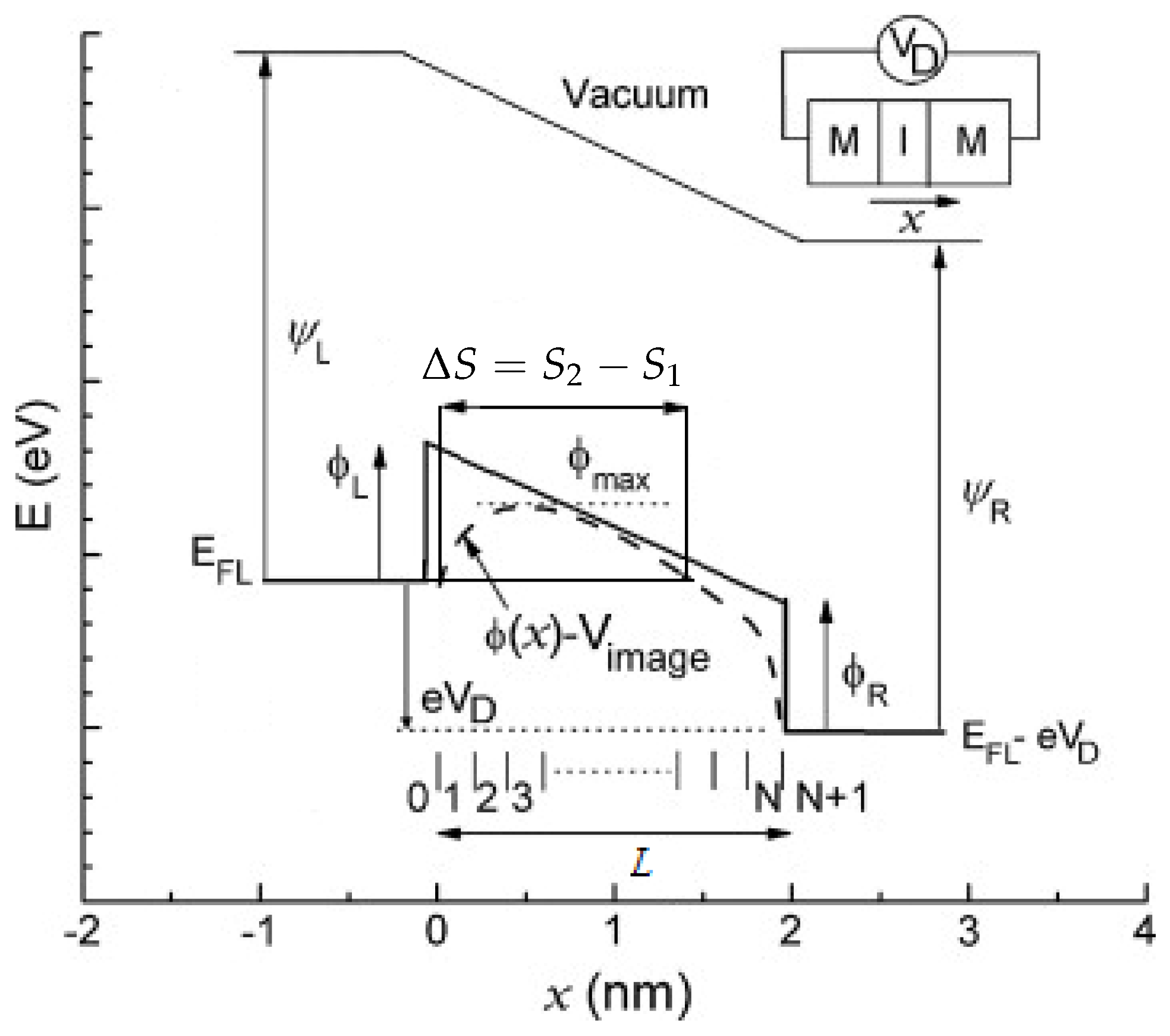
- The modeled structure is a one-dimensional structure such that the modeled diode metal insulator interface infinitely extends and that the potential value changes only in one direction normal to the interface.
- The Schrödinger wave equation time is approximated using Bastard’s assumption [54] in which case all the rapid changes of the wave function with respect to time are neglected, and the wave function becomes as shown in (5). This simplification allows one to treat the wave function as a time-independent parameter.
- The simplified wave function, which is now only space-dependent, is further divided into two components, according to Euler’s formulas. As shown in (6) for the j-th cell. and can be determined through the boundary conditions of the wave function, and is a complex function whose value can be determined from [53] (6).
4.1.2. Under Illumination
4.2. Geometric Devices
4.3. Hybrid Diodes
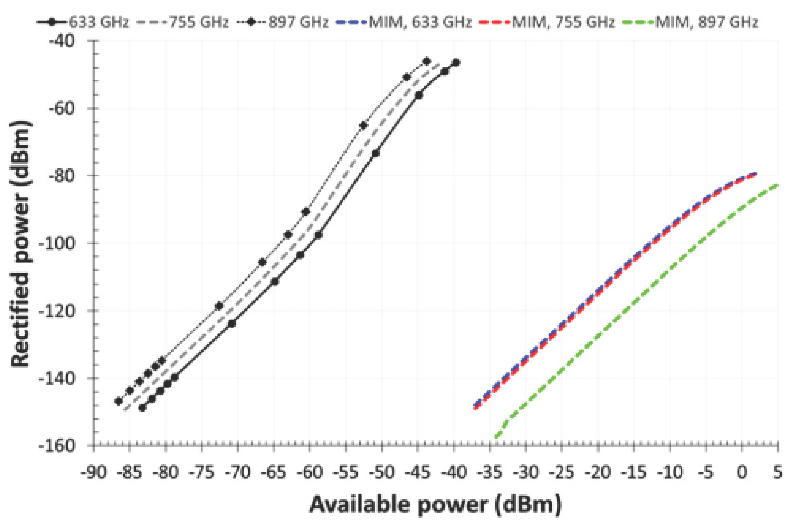
5. Power Level
5.1. Signal Amplitude
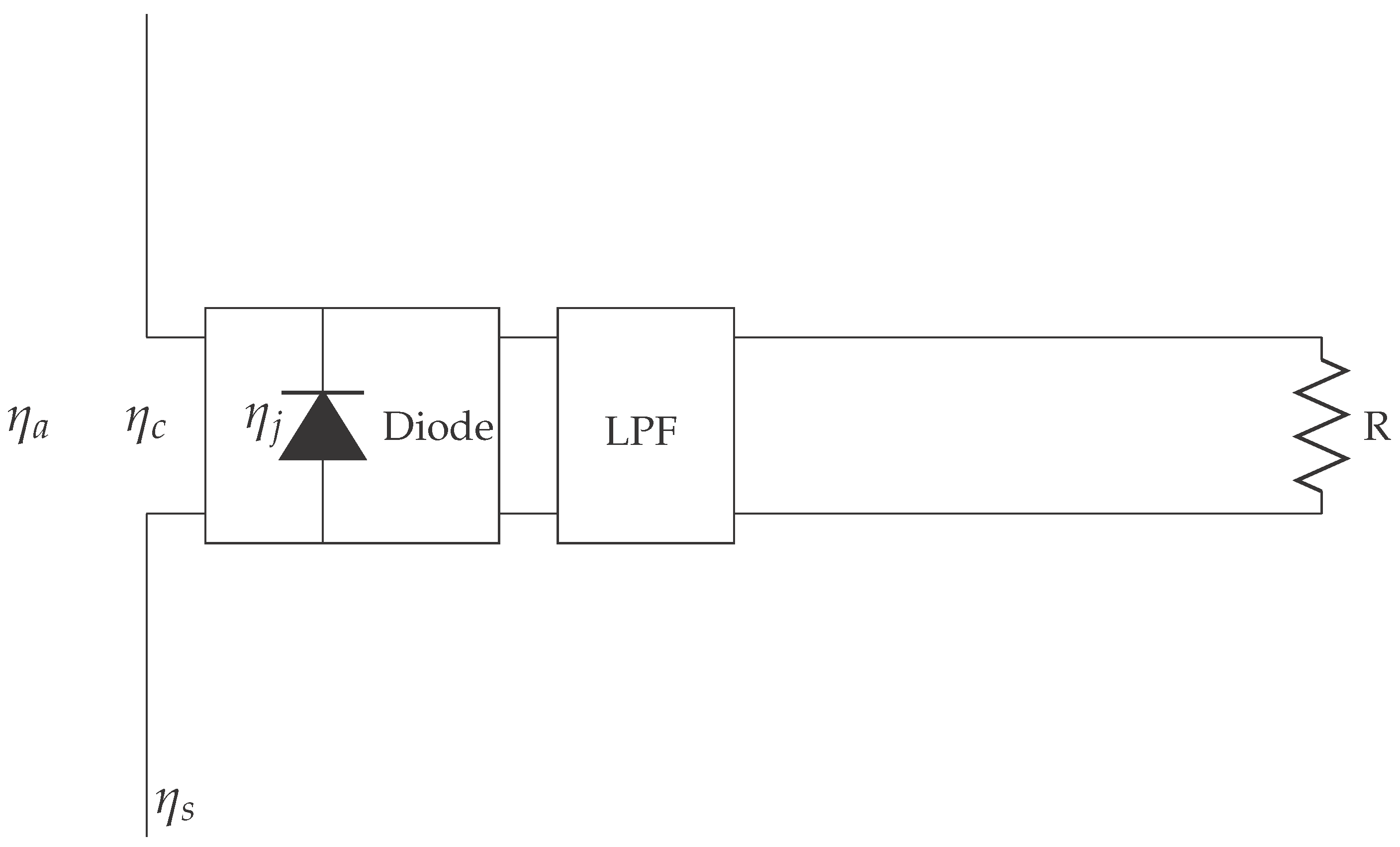
- Rectifiers: where it is of a major importance to express a good level of nonlinearity within the working range to increase the rectification efficiency for the harvested energy. In order to quantitatively characterize the diodes as efficient rectifiers, Donchev et al. [19] reinforced what has been set by [50,85,86] as the criteria that a diode should satisfy to be considered a rectifier. The rectifier figures of merit are asymmetry , nonlinearity and responsivity . They can be calculated using (21)–(23), respectively. In these equations, the current is represented as a function of voltage ; forward and reverse current values for the same voltage absolute value are and , respectively. The minimum figures of merit values required are shown next to the respective equations. Having said that, it should be noted that these devices are, after all, nonlinear where it is better to be approached subjectively. This means that these ruling figures are just for guidance, and each device design would have its own characteristics.
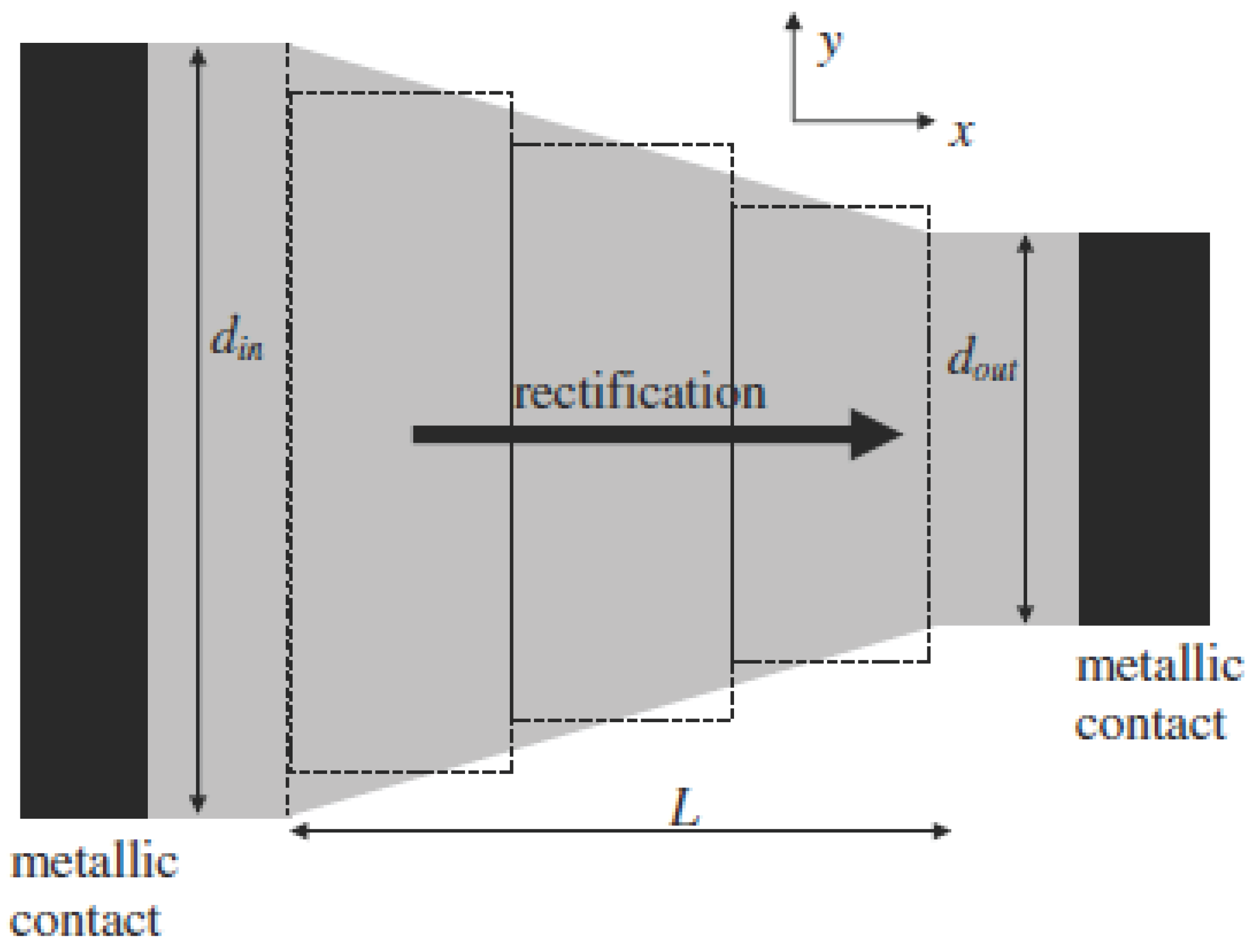
5.2. Received Wave Bandwidth
5.2.1. Impact from the Incident Wave
5.2.2. Impact from the Rectifier Device
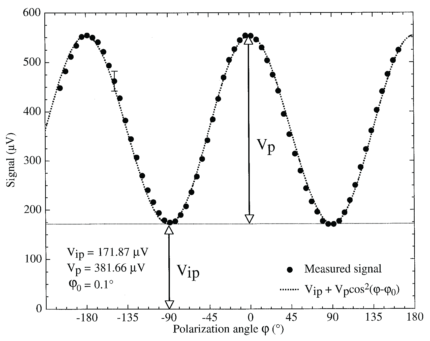
5.3. Polarization
6. Thermal Effect
6.1. Thermionic Effect
6.2. Seebeck Effect
6.3. Other Thermal Effects
7. Fabrication Aspects
7.1. Current Lithographic Techniques
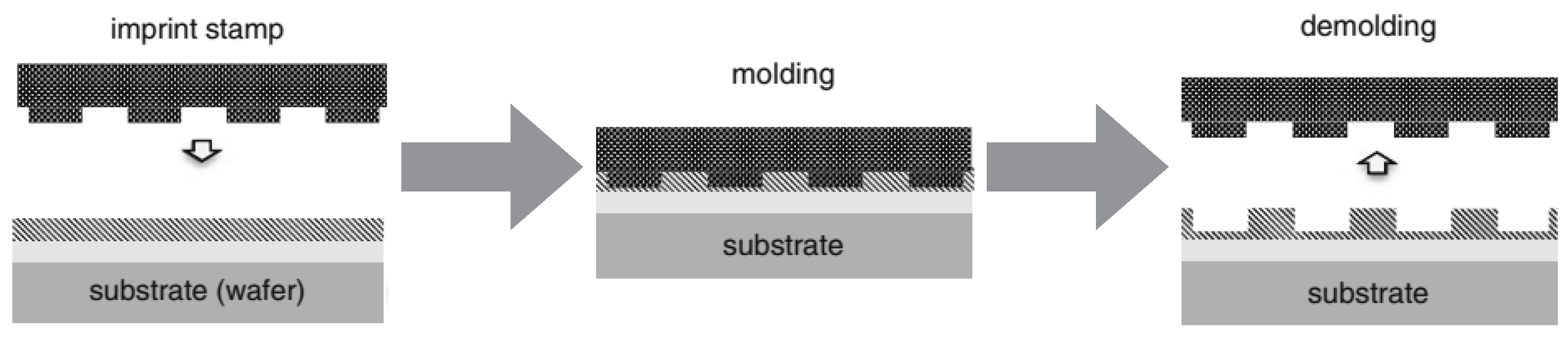
7.2. Nano Imprint Lithography
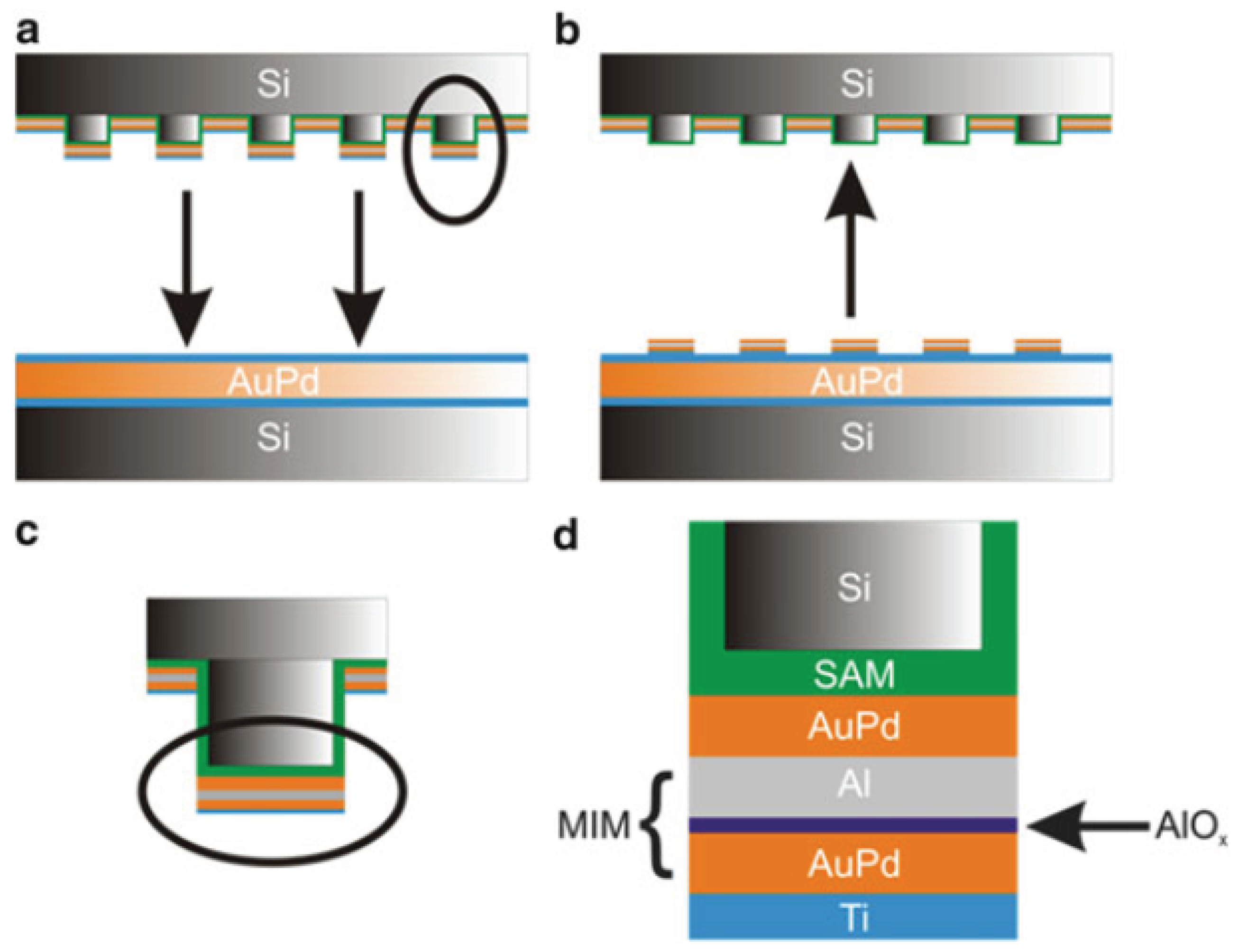
7.3. Mechanical Nano Imprint Lithography
7.4. Roll to Roll Manufacturing
7.5. Nano Transfer Print
8. Conclusions
Author Contributions
Conflicts of Interest
References
- Landis, F.; Schenker, O.; Tovar Reaños, M.; Vonnahme, C.; Zitzelsberger, S. An Overview on Current Climate Policies in the European Union and its Member States; ENTRACTE Project Report; ENTRACTE: Washington, DC, USA, 2013. [Google Scholar]
- WWF. How Low? Achieving Optimal Carbon Savings from the UK’s Existing Housing Stock; WWF: Grand, Switzerland, 2008. [Google Scholar]
- Corkish, R.; Green, M.; Puzzer, T. Solar energy collection by antennas. Sol. Energy 2002, 73, 395–401. [Google Scholar] [CrossRef]
- Brown, W.C. Optimization of the Efficiency and Other Properties of the Rectenna Element. In Proceedings of the IEEE-MTT-S International Microwave Symposium, Cherry Hill, NJ, USA, 14–16 June 1976; pp. 142–144. [Google Scholar]
- Berland, B. Photovoltaic Technologies Beyond the Horizon: Optical Rectenna Solar Cell, Final Report, 1 August 2001–30 September 2002; Technical Report; National Renewable Energy Lab.: Golden, CO, USA, 2003.
- Edmond Becquerel. Available online: https://en.wikipedia.org/w/index.php?title=Edmond_Becquerel&oldid=791838776 (accessed on 7 August 2017).
- Anonymous April 25, 1954: Bell Labs Demonstrates the First Practical Silicon Solar Cell. APS Phys. 2009, 18.
- Li, Y. Synthesis, Characterization, and Photovoltaic Applications of Mesoscopic Phthalocyanine Structures. Ph.D. Thesis, Electrical Engineering and Computer Science Department, South Dakota State University, Brookings, SD, USA, 2011. [Google Scholar]
- Shockley, W.; Queisser, H.J. Detailed balance limit of efficiency of p-n junction solar cells. J. Appl. Phys. 1961, 32, 510–519. [Google Scholar] [CrossRef]
- Sohrabi, F.; Nikniazi, A.; Movla, H. Optimization of Third Generation Nanostructured Silicon- Based Solar Cells. In Solar Cells—Research and Application Perspectives; Morales-Acevedo, A., Ed.; InTech: Rijeka, Croatia, 2013; Chapter 01. [Google Scholar]
- Kazmerski, L.; Gwinner, D.; Hicks, A. Best research cell efficiencies. Natl. Renew. Energy Lab. 2010, 2. [Google Scholar]
- King, R.; Law, D.; Edmondson, K.; Fetzer, C.; Kinsey, G.; Yoon, H.; Sherif, R.; Karam, N. 40% efficient metamorphic GaInP/GaInAs/Ge multijunction solar cells. Appl. Phys. Lett. 2007, 90, 183516. [Google Scholar] [CrossRef]
- Michael, G.; Alan, G. A Manufacturing Cost Analysis Relevant to Single- and Dual-Junction Photovoltaic Cells Fabricated with III-Vs and III-Vs Grown on Czochralski Silicon; Report; NREL: Washington, DC, USA, 2013.
- Yang, Y.; You, J. Make perovskite solar cells stable. Nature 2017, 544, 155–156. [Google Scholar] [CrossRef] [PubMed]
- Brown, W.C. The Microwave Powered Helicopter. J. Microw. Power 1966, 1, 1–20. [Google Scholar] [CrossRef]
- Moddel, G.; Grover, S. Rectenna Solar Cells; Moddel, G., Grover, S., Eds.; Springer: New York, NY, USA, 2013; 399p. [Google Scholar]
- Koert, P.; Cha, J.; Machina, M. 35 and 94 GHz rectifying antenna systems. In SPS 91-Power from Space; Société des Electriciens et des Electroniciens: Paris, France, 1991; pp. 541–547. [Google Scholar]
- Chiou, H.K.; Chen, I.S. High-Efficiency Dual-Band On-Chip Rectenna for 35-and 94-GHz Wireless Power Transmission in 0.13-m CMOS Technology. IEEE Trans. Microw. Theory Tech. 2010, 58, 3598–3606. [Google Scholar] [CrossRef]
- Donchev, E.; Pang, J.S.; Gammon, P.M.; Centeno, A.; Xie, F.; Petrov, P.K.; Breeze, J.D.; Ryan, M.P.; Riley, D.J.; Alford, N.M. The rectenna device: From theory to practice (a review). MRS Energy Sustain. 2014, 1. [Google Scholar] [CrossRef]
- Moddel, G. Will rectenna solar cells be practical? In Rectenna Solar Cells; Springer: Berlin, Germany, 2013; pp. 3–24. [Google Scholar]
- Konopsky, V.N.; Alieva, E.V. Long-range plasmons in lossy metal films on photonic crystal surfaces. Opt. Lett. 2009, 34, 479–481. [Google Scholar] [CrossRef] [PubMed]
- Optical Rectenna. Available online: https://en.wikipedia.org/w/index.php?title=Optical_rectenna&oldid=791785571 (accessed on 11 August 2017).
- Iluz, Z.; Boag, A. Dual-Vivaldi wideband nanoantenna with high radiation efficiency over the infrared frequency band. Opt. Lett. 2011, 36, 2773–2775. [Google Scholar] [CrossRef] [PubMed]
- Sabaawi, A.M.; Tsimenidis, C.C.; Sharif, B.S. Overview of nanoantennas for solar rectennas. In Rectenna Solar Cells; Springer: Berlin, Germany, 2013; pp. 231–256. [Google Scholar]
- Masotti, D.; Costanzo, A.; Rusticelli, S.; Tartarini, G.; Aldrigo, M. Infrared nano-rectennas exploiting on-demand laser sources. In Proceedings of the 2014 IEEE RFID Technology and Applications Conference (RFID-TA), Tampere, Finland, 8–9 September 2014; pp. 17–20. [Google Scholar]
- Grover, S.; Moddel, G. Optical frequency rectification. In Rectenna Solar Cells; Springer: Berlin, Germany, 2013; pp. 25–46. [Google Scholar]
- Russer, J.A.; Jirauschek, C.; Szakmany, G.P.; Schmidt, M.; Orlov, A.O.; Bernstein, G.H.; Porod, W.; Lugli, P.; Russer, P. High-Speed Antenna-Coupled Terahertz Thermocouple Detectors and Mixers. IEEE Trans. Microw. Theory Tech. 2015, 63, 4236–4246. [Google Scholar] [CrossRef]
- Fumeaux, C.; Herrmann, W.; Kneubühl, F.K.; Rothuizen, H. Nanometer thin-film Ni–NiO–Ni diodes for detection and mixing of 30 THz radiation. Infrared Phys. Technol. 1998, 39, 123–183. [Google Scholar] [CrossRef]
- Masotti, D.; Costanzo, A.; Aldrigo, M.; Dragoman, M. Graphene-based nano-rectennain the far infrared frequency band. In Proceedings of the 2014 44th European Microwave Conference, Rome, Italy, 6–9 October 2014. [Google Scholar]
- Dragoman, M.; Aldrigo, M.; Dinescu, A.; Dragoman, D.; Costanzo, A. Towards a terahertz direct receiver based on graphene up to 10 THz. J. Appl. Phys. 2014, 115. [Google Scholar] [CrossRef]
- Vakil, A.; Bajwa, H. Energy harvesting using Graphene based antenna for UV spectrum. In Proceedings of the 2014 IEEE Long Island Systems, Applications and Technology Conference (LISAT), Farmingdale, NY, USA, 2 May 2014; pp. 1–4. [Google Scholar]
- Byrnes, S.J.; Blanchard, R.; Capasso, F. Harvesting renewable energy from Earth’s mid-infrared emissions. Proc. Natl. Acad. Sci. USA 2014, 111, 3927–3932. [Google Scholar] [CrossRef] [PubMed]
- Kopp, G.; Lean, J.L. A new, lower value of total solar irradiance: Evidence and climate significance. Geophys. Res. Lett. 2011, 38. [Google Scholar] [CrossRef]
- Mashaal, H.; Gordon, J.M. Solar and thermal aperture antenna coherence performance limits. In Rectenna Solar Cells; Springer: Berlin, Germany, 2013; pp. 69–86. [Google Scholar]
- Thermionic Emission. Available online: https://en.wikipedia.org/w/index.php?title=Thermionic_emission&oldid=789623260 (accessed on 14 August 2017).
- Mayer, A.; Chung, M.; Weiss, B.; Miskovsky, N.; Cutler, P. Three-dimensional analysis of the rectifying properties of geometrically asymmetric metal-vacuum-metal junctions treated as an oscillating barrier. Phys. Rev. B 2008, 78, 205404. [Google Scholar] [CrossRef]
- Conley, J.F., Jr.; Alimardani, N. Impact of Electrode Roughness on Metal-Insulator-Metal (MIM) Diodes and Step Tunneling in Nanolaminate Tunnel Barrier Metal-Insulator-Insulator-Metal (MIIM) Diodes. In Rectenna Solar Cells; Springer: Berlin, Germany, 2013; pp. 111–134. [Google Scholar]
- HyperPhysics. Wien’s Displacement Law. 2006. Available online: http://hyperphysics.phy-astr.gsu.edu/hbase/wien.html (accessed on 14 August 2017).
- Tucker, J.R.; Feldman, M.J. Quantum detection at millimeter wavelengths. Rev. Modern Phys. 1985, 57, 1055. [Google Scholar] [CrossRef]
- Habbal, F.; Danchi, W.C.; Tinkham, M. Photon-assisted tunneling at 246 and 604 GHz in small-area superconducting tunnel junctions. Appl. Phys. Lett. 1983, 42, 296–298. [Google Scholar] [CrossRef]
- O’Regan, T.; Chin, M.; Tan, C.; Birdwell, A. Modeling, Fabrication, and Electrical Testing of Metal-Insulator-Metal Diode; Technical Report; Army Research Lab Adelphi Md Sensors and Electron Devices Directorate: Adelphi, MD, USA, 2011. [Google Scholar]
- Hathaikarn, M. Electrical Properties of Niobium Based Oxides-Ceramics and Single Crystal Fibers Grown by the Laser-Heated Pedestal Growth (LHPG) Technique. Ph.D. Thesis, The Graduate School Intercollege Graduate Program in Materials, The Pennsylvania State University, Centre County, PA, USA, 2003; p. 319. [Google Scholar]
- Polyanskiy, M.N. Available online: https://refractiveindex.info (accessed on 30 August 2017).
- Simmons, J.G. Generalized formula for the electric tunnel effect between similar electrodes separated by a thin insulating film. J. Appl. Phys. 1963, 34, 1793–1803. [Google Scholar] [CrossRef]
- Sanchez, A.; Davis, C., Jr.; Liu, K.; Javan, A. The MOM tunneling diode: Theoretical estimate of its performance at microwave and infrared frequencies. J. Appl. Phys. 1978, 49, 5270–5277. [Google Scholar] [CrossRef]
- Heiblum, M.; Wang, S.; Whinnery, J.; Gustafson, T. Characteristics of integrated MOM junctions at dc and at optical frequencies. IEEE J. Quantum Electron. 1978, 14, 159–169. [Google Scholar] [CrossRef]
- Grover, S.; Moddel, G. Engineering the current–voltage characteristics of metal–insulator–metal diodes using double-insulator tunnel barriers. Solid-State Electron. 2012, 67, 94–99. [Google Scholar] [CrossRef]
- Smythe, W.R. Static and Dynamic Electricity; McGraw-Hill Book Company, Inc.: New York, NY, USA, 1950. [Google Scholar]
- Miller, S.C., Jr.; Good, R., Jr. A WKB-type approximation to the Schrödinger equation. Phys. Rev. 1953, 91, 174. [Google Scholar] [CrossRef]
- Chin, M.L.; Periasamy, P.; O’Regan, T.P.; Amani, M.; Tan, C.; O’Hayre, R.P.; Berry, J.J.; Osgood, R.M., III; Parilla, P.A.; Ginley, D.S. Planar metal–insulator–metal diodes based on the Nb/Nb2O5/X material system. J. Vac. Sci. Technol. B Nanotechnol. Microelectron. Mater. Process. Meas. Phenom. 2013, 31. [Google Scholar] [CrossRef]
- Koppinen, P. Bias and Temperature Dependence Analysis of the Tunneling Current of Normal Metal-Insulator-Normal Metal Tunnel Junctions. Master’s Thesis, Departmment of Physics, University of Jyväskylä, Jyväskylä, Finland, 2003. [Google Scholar]
- Transfer-Matrix Method (Optics). Available online: https://en.wikipedia.org/w/index.php?title=Transfermatrix_method_(optics)&oldid=792683168 (accessed on 17 August 2017).
- Jonsson, B.; Eng, S.T. Solving the Schrodinger equation in arbitrary quantum-well potential profiles using the transfer matrix method. IEEE J. Quantum Electron. 1990, 26, 2025–2035. [Google Scholar] [CrossRef]
- Bastard, G. Superlattice band structure in the envelope-function approximation. Phys. Rev. B 1981, 24, 5693. [Google Scholar] [CrossRef]
- Jirauschek, C. Accuracy of transfer matrix approaches for solving the effective mass Schrödinger equation. IEEE J. Quantum Electron. 2009, 45, 1059–1067. [Google Scholar] [CrossRef]
- Hashem, I.E.; Rafat, N.H.; Soliman, E.A. Theoretical study of metal-insulator-metal tunneling diode figures of merit. IEEE J. Quantum Electron. 2013, 49, 72–79. [Google Scholar] [CrossRef]
- Burt, M. Fundamentals of envelope function theory for electronic states and photonic modes in nanostructures. J. Phys. Condens. Matter 1999, 11, 53. [Google Scholar] [CrossRef]
- Lent, C.S.; Kirkner, D.J. The quantum transmitting boundary method. J. Appl. Phys. 1990, 67, 6353–6359. [Google Scholar] [CrossRef]
- Filipovic, L.; Stanojevic, Z.; Baumgartner, O.; Kosina, H. 3D modeling of direct band-to-band tunneling in nanowire TFETs. Energy 2014, 1, 1–5. [Google Scholar]
- Paulsson, M. Non equilibrium green’s functions for dummies: Introduction to the one particle NEGF equations. arXiv, 2002; arXiv:cond-mat/0210519. [Google Scholar]
- Perturbation Theory (Quantum Mechanics). Available online: https://en.wikipedia.org/w/index.php?title=Perturbation_theory_(quantum_mechanics)&oldid=793439215 (accessed on 19 August 2017).
- Grover, S.; Moddel, G. Metal single-insulator and multi-insulator diodes for rectenna solar cells. In Rectenna Solar Cells; Springer: Berlin, Germany, 2013; pp. 89–109. [Google Scholar]
- Datta, S.; Anantram, M. Steady-state transport in mesoscopic systems illuminated by alternating fields. Phys. Rev. B 1992, 45, 13761. [Google Scholar] [CrossRef]
- Zhu, Z.; Joshi, S.; Grover, S.; Moddel, G. Geometric diodes for optical rectennas. In Rectenna Solar Cells; Springer: Berlin, Germany, 2013; pp. 209–227. [Google Scholar]
- Tien, P.; Gordon, J. Multiphoton process observed in the interaction of microwave fields with the tunneling between superconductor films. Phys. Rev. 1963, 129, 647. [Google Scholar] [CrossRef]
- Joshi, S.; Moddel, G. Efficiency limits of rectenna solar cells: Theory of broadband photon-assisted tunneling. Appl. Phys. Lett. 2013, 102, 083901. [Google Scholar] [CrossRef]
- Floquet Theory. Available online: https://en.wikipedia.org/w/index.php?title=Floquet_theory&oldid=790708503 (accessed on 21 August 2017).
- Grifoni, M.; Hänggi, P. Driven quantum tunneling. Phys. Rep. 1998, 304, 229–354. [Google Scholar] [CrossRef]
- Truscott, W. Wave functions in the presence of a time-dependent field: Exact solutions and their application to tunneling. Phys. Rev. Lett. 1993, 70, 1900. [Google Scholar] [CrossRef] [PubMed]
- Büttiker, M.; Landauer, R. Traversal time for tunneling. Phys. Rev. Lett. 1982, 49, 1739. [Google Scholar] [CrossRef]
- Liu, H. Time-dependent approach to double-barrier quantum well oscillators. Appl. Phys. Lett. 1988, 52, 453–455. [Google Scholar] [CrossRef]
- Zhu, Z.J. Graphene Geometric Diodes for Optical Rectennas. Ph.D. Thesis, University of Colorado at Boulder, Boulder, CO, USA, 2014. [Google Scholar]
- Han, M.Y.; Özyilmaz, B.; Zhang, Y.; Kim, P. Energy band-gap engineering of graphene nanoribbons. Phys. Rev. Lett. 2007, 98, 206805. [Google Scholar] [CrossRef] [PubMed]
- Dragoman, D.; Dragoman, M. Geometrically induced rectification in two-dimensional ballistic nanodevices. J. Phys. D Appl. Phys. 2013, 46, 055306. [Google Scholar] [CrossRef]
- Dirac Equation. Available online: https://en.wikipedia.org/w/index.php?title=Dirac_equation&oldid=796044311 (accessed on 21 August 2017).
- Dragoman, M.; Dinescu, A.; Dragoman, D. On-wafer graphene diodes for high-frequency applications. In Proceedings of the European IEEE Solid-State Device Research Conference (ESSDERC), Bucharest, Romania, 16–20 September 2013; pp. 322–325. [Google Scholar]
- Stellingwerff, S.A. Solar Energy Harvesting Using Graphene Rectennas: A Proof-of-Concept Study. Master’s Thesis, University of Twente, Enschede, The Netherlands, 2015. [Google Scholar]
- Tongay, S.; Lemaitre, M.; Miao, X.; Gila, B.; Appleton, B.; Hebard, A. Rectification at graphene-semiconductor interfaces: Zero-Gap semiconductor-based diodes. Phys. Rev. X 2012, 2, 011002. [Google Scholar] [CrossRef]
- Dragoman, M.; Aldrigo, M. Graphene rectenna for efficient energy harvesting at terahertz frequencies. Appl. Phys. Lett. 2016, 109, 113105. [Google Scholar] [CrossRef]
- Torrey, H.; Whitmer, C. Crystal Rectifiers; McGra∖v-Hill: New York, NY, USA, 1948; p. 948. [Google Scholar]
- Gillespie, D.J.; Ellis, D.P. Modeling nonlinear circuits with linearized dynamical models via kernel regression. In Proceedings of the 2013 IEEE Workshop on Applications of Signal Processing to Audio and Acoustics (WASPAA), New Paltz, NY, USA, 20–23 October 2013; pp. 1–4. [Google Scholar]
- Rizzoli, V.; Lipparini, A.; Costanzo, A.; Mastri, F.; Cecchetti, C.; Neri, A.; Masotti, D. State-of-the-art harmonic-balance simulation of forced nonlinear microwave circuits by the piecewise technique. IEEE Trans. Microw. Theory Tech. 1992, 40, 12–28. [Google Scholar] [CrossRef]
- Briones, E.; Briones, J.; Martinez-Anton, J.; Cuadrado, A.; McMurtry, S.; Hehn, M.; Montaigne, F.; Alda, J.; González, J. Seebeck nanoantennas for infrared detection and energy harvesting applications. In Proceedings of the 2015 9th European Conference on Antennas and Propagation (EuCAP), Lisbon, Portugal, 12–17 April 2015; pp. 1–4. [Google Scholar]
- Russer, J.A.; Jirauschek, C.; Szakmany, G.P.; Schmidt, M.; Orlov, A.O.; Bernstein, G.H.; Porod, W.; Lugli, P.; Russer, P. A nanostructured long-wave infrared range thermocouple detector. IEEE Trans. Terahertz Sci. Technol. 2015, 5, 335–343. [Google Scholar] [CrossRef]
- Periasamy, P.; Guthrey, H.L.; Abdulagatov, A.I.; Ndione, P.F.; Berry, J.J.; Ginley, D.S.; George, S.M.; Parilla, P.A.; O’Hayre, R.P. Metal–insulator–metal diodes: Role of the insulator layer on the rectification performance. Adv. Mater. 2013, 25, 1301–1308. [Google Scholar] [CrossRef] [PubMed]
- Periasamy, P.; Berry, J.J.; Dameron, A.A.; Bergeson, J.D.; Ginley, D.S.; O’Hayre, R.P.; Parilla, P.A. Fabrication and characterization of MIM diodes based on Nb/Nb2O5 via a rapid screening technique. Adv. Mater. 2011, 23, 3080–3085. [Google Scholar] [CrossRef] [PubMed]
- Mitrovic, I.Z.; Weerakkody, A.D.; Sedghi, N.; Hall, S.; Ralph, J.F.; Wrench, J.S.; Chalker, P.R.; Luo, Z.; Beeby, S. (Invited) Tunnel-Barrier Rectifiers for Optical Nantennas. ECS Trans. 2016, 72, 287–299. [Google Scholar] [CrossRef]
- Divitt, S.; Novotny, L. Spatial coherence of sunlight and its implications for light management in photovoltaics. Optica 2015, 2, 95–103. [Google Scholar] [CrossRef]
- Thermophotovoltaic. Available online: https://en.wikipedia.org/w/index.php?title=Thermophotovoltaic&oldid=793300523 (accessed on 23 August 2017).
- Lenert, A.; Bierman, D.M.; Nam, Y.; Chan, W.R.; Celanović, I.; Soljačić, M.; Wang, E.N. A nanophotonic solar thermophotovoltaic device. Nat. Nanotechnol. 2014, 9, 126–130. [Google Scholar] [CrossRef] [PubMed]
- Harder, N.P.; Würfel, P. Theoretical limits of thermophotovoltaic solar energy conversion. Semicond. Sci. Technol. 2003, 18, S151. [Google Scholar] [CrossRef]
- DeMeo, D.F.; Licht, A.S.; Shemelya, C.M.; Downs, C.M.; Vandervelde, T.E. Thermophotovoltaics: An alternative to and potential partner with rectenna energy harvesters. In Rectenna Solar Cells; Springer: Berlin, Germany, 2013; pp. 371–390. [Google Scholar]
- DiMatteo, R.; Greiff, P.; Seltzer, D.; Meulenberg, D.; Brown, E.; Carlen, E.; Kaiser, K.; Finberg, S.; Nguyen, H.; Azarkevich, J.; et al. Micron-gap Thermo Photo Voltaics (MTPV). AIP Conf. Proc. 2004, 738, 42–51. [Google Scholar]
- Carozzi, T.; Woan, G. A generalized measurement equation and van Cittert-Zernike theorem for wide-field radio astronomical interferometry. Mon. Not. R. Astron. Soc. 2009, 395, 1558–1568. [Google Scholar] [CrossRef]
- Zhu, Z.; Joshi, S.; Grover, S.; Moddel, G. Graphene geometric diodes for terahertz rectennas. J. Phys. D Appl. Phys. 2013, 46, 185101. [Google Scholar] [CrossRef]
- Bareiß, M.; Krenz, P.M.; Szakmany, G.P.; Tiwari, B.N.; Kalblein, D.; Orlov, A.O.; Bernstein, G.H.; Scarpa, G.; Fabel, B.; Zschieschang, U.; et al. Rectennas revisited. IEEE Trans. Nanotechnol. 2013, 12, 1144–1150. [Google Scholar]
- Simmons, J.G. Potential barriers and emission-limited current flow between closely spaced parallel metal electrodes. J. Appl. Phys. 1964, 35, 2472–2481. [Google Scholar] [CrossRef]
- Goldsmid, H.J. The Seebeck and Peltier effects. In The Physics of Thermoelectric Energy Conversion; 2053-2571; Morgan & Claypool Publishers: Williston, VT, USA, 2017; pp. 1-1–1-3. [Google Scholar]
- Das, V.D.; Soundararajan, N. Size and temperature effects on the Seebeck coefficient of thin bismuth films. Phys. Rev. B 1987, 35, 5990. [Google Scholar] [CrossRef]
- Li, G.; Han, D.; Yang, F.; Wang, Z.; Pi, Y.; Wang, W.; Xu, S. Linearly enhanced response of thermopower in cascaded array of dual-stripe single-metal thermocouples. Appl. Phys. Lett. 2017, 110, 203505. [Google Scholar] [CrossRef]
- Huhn, A.K.; Spickermann, G.; Ihring, A.; Schinkel, U.; Meyer, H.G.; Haring Bolívar, P. Uncooled antenna-coupled terahertz detectors with 22 μs response time based on BiSb/Sb thermocouples. Appl. Phys. Lett. 2013, 102, 121102. [Google Scholar] [CrossRef]
- Szakmany, G.P.; Orlov, A.O.; Bernstein, G.H.; Porod, W.; Bareiss, M.; Lugli, P.; Russer, J.A.; Jirauschek, C.; Russer, P.; Ivrlac, M.T.; et al. Nano-antenna arrays for the infrared regime. In Proceedings of the 18th International ITG Workshop on Smart Antennas (WSA), VDE, Erlangen, Germany, 12–13 March 2014; pp. 1–8. [Google Scholar]
- Cuadrado, A.; Alda, J.; González, F.J. Distributed bolometric effect in optical antennas and resonant structures. J. Nanophotonics 2012, 6. [Google Scholar] [CrossRef]
- Yang, W.; Zhou, W.; Ma, Z.; Berggren, J.; Hammar, M. Flexible solar cells based on stacked crystalline semiconductor nanomembranes on plastic substrates. In Proceedings of the 2010 Conference on Lasers and Electro-Optics (CLEO) and Quantum Electronics and Laser Science Conference (QELS), San Jose, CA, USA, 16–21 May 2010; p. CML2. [Google Scholar]
- Bjorkholm, J.E. EUV lithography—The successor to optical lithography. Intel Technol. J. 1998, 3, 98. [Google Scholar]
- Robinson, T.; Yi, D.; Brinkley, D.; Roessler, K.; White, R.; Bozak, R.; Archuletta, M.; Lee, D. Clean and repair of EUV photomasks. Proc. SPIE 2011, 8166. [Google Scholar] [CrossRef]
- Slafer, W.D. Techniques for Roll-to-Roll Manufacturing of Flexible Rectenna Solar Cells. In Rectenna Solar Cells; Springer: Berlin, Germany, 2013; pp. 337–369. [Google Scholar]
- Slafer, W.D. Tools and Methods for Producing Nanoantenna Electronic Devices. U.S. Patent 9,589,797, 7 March 2017. [Google Scholar]
- Bareiß, M.; Kälblein, D.; Krenz, P.M.; Zschieschang, U.; Klauk, H.; Scarpa, G.; Fabel, B.; Porod, W.; Lugli, P. Large-Area Fabrication of Antennas and Nanodiodes. In Rectenna Solar Cells; Springer: Berlin, Germany, 2013; pp. 297–311. [Google Scholar]
- Weiler, B.; Nagel, R.; Albes, T.; Haeberle, T.; Gagliardi, A.; Lugli, P. Electrical and morphological characterization of transfer-printed Au/Ti/TiO x/p+-Si nano-and microstructures with plasma-grown titanium oxide layers. J. Appl. Phys. 2016, 119, 145106. [Google Scholar] [CrossRef]
- Nagel, R.D.; Haeberle, T.; Schmidt, M.; Lugli, P.; Scarpa, G. Large Area Nano-transfer Printing of Sub-50-nm Metal Nanostructures Using Low-cost Semi-flexible Hybrid Templates. Nanoscale Res. Lett. 2016, 11, 143. [Google Scholar] [CrossRef] [PubMed]


© 2017 by the authors. Licensee MDPI, Basel, Switzerland. This article is an open access article distributed under the terms and conditions of the Creative Commons Attribution (CC BY) license (http://creativecommons.org/licenses/by/4.0/).
Share and Cite
Shanawani, M.; Masotti, D.; Costanzo, A. THz Rectennas and Their Design Rules. Electronics 2017, 6, 99. https://doi.org/10.3390/electronics6040099
Shanawani M, Masotti D, Costanzo A. THz Rectennas and Their Design Rules. Electronics. 2017; 6(4):99. https://doi.org/10.3390/electronics6040099
Chicago/Turabian StyleShanawani, Mazen, Diego Masotti, and Alessandra Costanzo. 2017. "THz Rectennas and Their Design Rules" Electronics 6, no. 4: 99. https://doi.org/10.3390/electronics6040099
APA StyleShanawani, M., Masotti, D., & Costanzo, A. (2017). THz Rectennas and Their Design Rules. Electronics, 6(4), 99. https://doi.org/10.3390/electronics6040099