Article

Online Optimal Switching Frequency Selection for Grid-Connected Voltage Source Inverters

1
Department of Electrical Engineering, Faculty of Engineering, Jordan University of Science and Technology, Irbid 22110, Jordan
2
Department of Electrical Power Engineering, Hijjawi Faculty for Engineering Technology, Yarmouk University, Irbid 21163, Jordan
*
Author to whom correspondence should be addressed.
Electronics 2017, 6(4), 110; https://doi.org/10.3390/electronics6040110
Submission received: 27 October 2017 / Revised: 2 December 2017 / Accepted: 11 December 2017 / Published: 15 December 2017
(This article belongs to the Special Issue Applications of Power Electronics)

Abstract

:
Enhancing the performance of the voltage source inverters (VSIs) without changing the hardware structure has recently acquired an increased amount of interest. In this study, an optimization algorithm, enhancing the quality of the output power and the efficiency of three-phase grid connected VSIs is proposed. Towards that end, the proposed algorithm varies the switching frequency (fsw) to maintain the best balance between switching losses of the insulated-gate-bipolar-transistor (IGBT) power module as well as the output power quality under all loading conditions, including the ambient temperature effect. Since there is a contradiction with these two measures in relation to the switching frequency, the theory of multi-objective optimization is employed. The proposed algorithm is executed on the platform of Altera® DE2-115 field-programmable-gate-array (FPGA) in which the optimal value of the switching frequency is determined online without the need for heavy offline calculations and/or lookup tables. With adopting the proposed algorithm, there is an improvement in the VSI efficiency without degrading the output power quality. Therefore, the proposed algorithm enhances the lifetime of the IGBT power module because of reduced variations in the module’s junction temperature. An experimental prototype is built, and experimental tests are conducted for the verification of the viability of the proposed algorithm.

1. Introduction

Renewable energy resources play a major role in the current world’s energy generation. To interconnect renewable energy resources, grid connected three-phase VSIs are widely utilized [1]. However, the increased number of connections between the VSIs and the grid should never degrade the power quality, particularly at the point of common coupling (PCC), while the total harmonic distortion (THD) should never go beyond a specific limit to prevent harmonics related problems. It is possible to reduce the THD with the switching frequency (fsw) being increased. However, when the fsw is increased, the switching losses are likewise increased and, therefore, this can result in a reduction in the inverter’s efficiency as well. Consequently, fsw is typically, but not optimally, chosen as a trade-off between the output power quality and the efficiency at a specific loading condition. Since the operating conditions of the VSI are continuously varying, the variable switching frequency (VSF) enables the inverter switching losses to be decreased in regions where the harmonic content is insignificant, and, in the same sense, the harmonic content can be reduced in the regions where the inverter losses are highly insignificant.
The performance of the three-phase grid connected VSIs is highly dependent on the selected fsw. Therefore, literature has proposed numerous algorithms of the VSF to enhance the inverter’s efficiency [2,3], inverter’s transient response [4], and the acoustic noise of induction motor [5]. Switching frequency is varied either within the fundamental period [6,7,8,9], or based on the operating conditions [10,11,12], such that the switching losses or the THD are minimized. In [6], the proposed algorithm is formulated based on the current-ripple analysis of the three-phase inverters in a time-domain. The idea was geared toward the reduction of fsw, while maintaining the peak current ripple under a certain limit; consequently, there is a reduction in the average fsw, and thus a reduction in switching losses. Application of the above algorithm can be found in [7,8] as well. In [9], the switching frequency trajectory was derived using calculus of variations and based on the current ripples analysis relative to the single-phase inverters in time-domain, in order to reduce the switching losses while meeting certain THD requirements. This method suffers from computational complexity and requires heavy offline calculations. In [10], the efficiency of single-phase inverter is incrementally enhanced, while satisfying standard THD; the result of the algorithm was an increase in the efficiency of the inverter in comparison with the conventional sinusoidal pulse-width modulation (SPWM) as well as the space-vector pulse-width modulation (SVPWM). In any case, the aim of the aforementioned methods was to enhance the efficiency of the inverter, while ensuring that the THD is continuously positioned to the highest allowable limit. An offline technique was proposed by the authors of [11] for the minimization of the losses of VSIs based on multi-objective optimization, where the proposed algorithm was used to control synchronous motors. Meanwhile, the target is characterized based on the weighted combination of the peak-to-peak ripple of electromagnetic torque and switching losses, in a way that a fair balance is achieved. In [12], an optimization process was applied on the electric and hybrid vehicle motor drive, in which fsw was varied with different modulation indices or input voltages. Concurrent switching losses minimization and dead-time compensation study was presented in [13] under various power levels and different power factors. Compared with discrete pulse width modulation techniques, switching losses were reduced by 15%.
The switching losses were reduced at high current-levels in [14] by proposing new SVPWM strategies in which the number of switch commutations of the quasi-Z-source inverter is reduced. In [15], a lower number of commutations is achieved by the proposed optimization. The variable switching frequency reduces about 19% of the switching losses compared with constant switching frequency for similar output current quality. Analytical variable switching frequency is presented in [16] according to the modulation index and a predefined current ripple band. The switching frequency varies within the fundamental cycle (sub-fundamental) to reduce the switching losses of two level inverter traction drive system. In [17], the switching loss is analyzed under different discontinuous SVPWM techniques for balanced two-phase load fed by a three-leg inverter. The algorithm tried to balance the switching losses of each phase-leg at lower current ripple. In [18], 3D-SVPWM of four-leg VSI was presented to reduce the switching losses of the proposed shunt compensator by 33%. The efficiency of a grid-tied full bridge inverter is improved in [19] using the variable switching frequency scheme. The authors minimize the switching losses at predefined THD using a bipolar modulation scheme. Variable switching frequency was used in [20] to reduce switching losses and electromagnetic interference (EMI) noise of a common voltage oriented SPWM rectifier considering the restrictions on voltage ripple at the direct current (DC) link.
The THD and the maximum torque ripple of the permanent magnet synchronous machine are optimized in [21]. For this target, the authors presented a finite control set model based on a predictive control scheme. A new behavioral model for losses in power semiconductors was proposed in [22] where the impacts of gate resistance and gate voltage are considered. A summary of the several behavioral models existing in literature and industry was listed.
The major contribution this paper puts in place is the proposition of an efficient and practically sound VSF algorithm whereby there is an online variation of fsw at various loading conditions, including the ambient temperature effect. The intensive calculations that are typically required with the exiting fsw variation-laws are avoided in the proposed algorithm. Moreover, the benefits of the proposed algorithm include the improvement of the inverters’ switching devices and packaging reliability by reducing the variations in the junction temperature, which has a direct effect on the lifetime of the inverter. The attractiveness of this algorithm lies in its simplicity, in which the online computation of the optimal switching frequency can be easily done. Most of the algorithms that have been introduced in the literature suffer from computational complexity that makes them lack practical sound. The advantages of this new proposed algorithms can be summarized in four main points: (1) easy to be implemented using micro-controllers; and (2) the proposed procedure can be generalized for any power converter that includes multi-level inverters regardless of the control mode and the used technology of the power device. However, the proposed mathematical derivations are discussed on an IGBT power module of Infineon® FP50R06KE3 (Neubiberg, Germany). The same procedures are valid for different technologies that have different power loss analysis. (3) The proposed procedure does not require offline computations and lookup tables; and, (4) since the temperature is considered in the proposed algorithm, the algorithm can reduce the thermal stress on the inverter during high ambient temperature by reducing the switching frequency. Conversely, if the energy loss parameters are not directly given from the manufacturer datasheets, the parameters can be experimentally characterized.
The remaining parts of this study are organized as follows. Short summary of the architecture and the control mode of operations of VSIs are presented in Section 2. Section 3 presents the estimation of power losses. Section 4 presents the thermal modeling of the IGBT power module. Section 5 presents the time-domain current ripple analysis. Section 6 presents the proposed variable switching algorithm. Section 7 presents a discussion of the experimental validation. Finally, Section 8 concludes the paper.

2. Voltage Source Inverters

VSIs are crucial components in the alternating current (AC) microgrids and modern power systems. To ensure power system reliability, integrating distribution generators (DGs) with existing power systems has some technical and practical constraints. One of these main limitations is power system stability. Voltage stability becomes more important if the microgrid is off-grid (i.e., isolated microgrid) or if connected with a relatively weak power system. The controllability of the VSIs and the DGs adds effective and supportive actions that can improve the performance of the power systems and microgrids in steady state and transient modes of operation [23].
VSIs can be categorized into three main modes of operation and control schemes. The first one is usually named as a grid-forming power converter in which the VSI is working as a conventional AC source. The voltage and the frequency are controlled and stabilized; however, the output current is load dependent. The uninterruptible power supply (UPS) is an appropriate example of grid-forming VSI. The UPS delivers certain voltage and frequency, where the input of the UPS is also considered as a DC, regardless of being from isolated batteries or converted from an online AC power supply.
The second category is known as grid-feeding power converters. Under this mode of operation, the voltage control is not targeted in the control scheme of the VSI. Moreover, the VSI is working as a current source to supply the desired real and reactive powers. Feeding an energized power system adds more restrictions to the VSI and synchronizing the voltage at PCC is crucially important to track the desired real and reactive power set points. In the previous two modes of operation, either the voltage or the current is controlled. For power system stability, it is occasionally important to control both the output voltage and current. This category is known as grid-supporting power converters and can be classified into two modes: (1) besides supplying the demanded active and reactive powers, it must contribute to stabilizing the voltage and/or the frequency of the grid-connected systems; and (2) the supplied active and reactive powers are subjected to the output voltage magnitude. The voltage magnitude and frequency have higher priority in the second mode than the first mode, and, hence, they can be implemented either in islanded or grid connected microgrids [23].
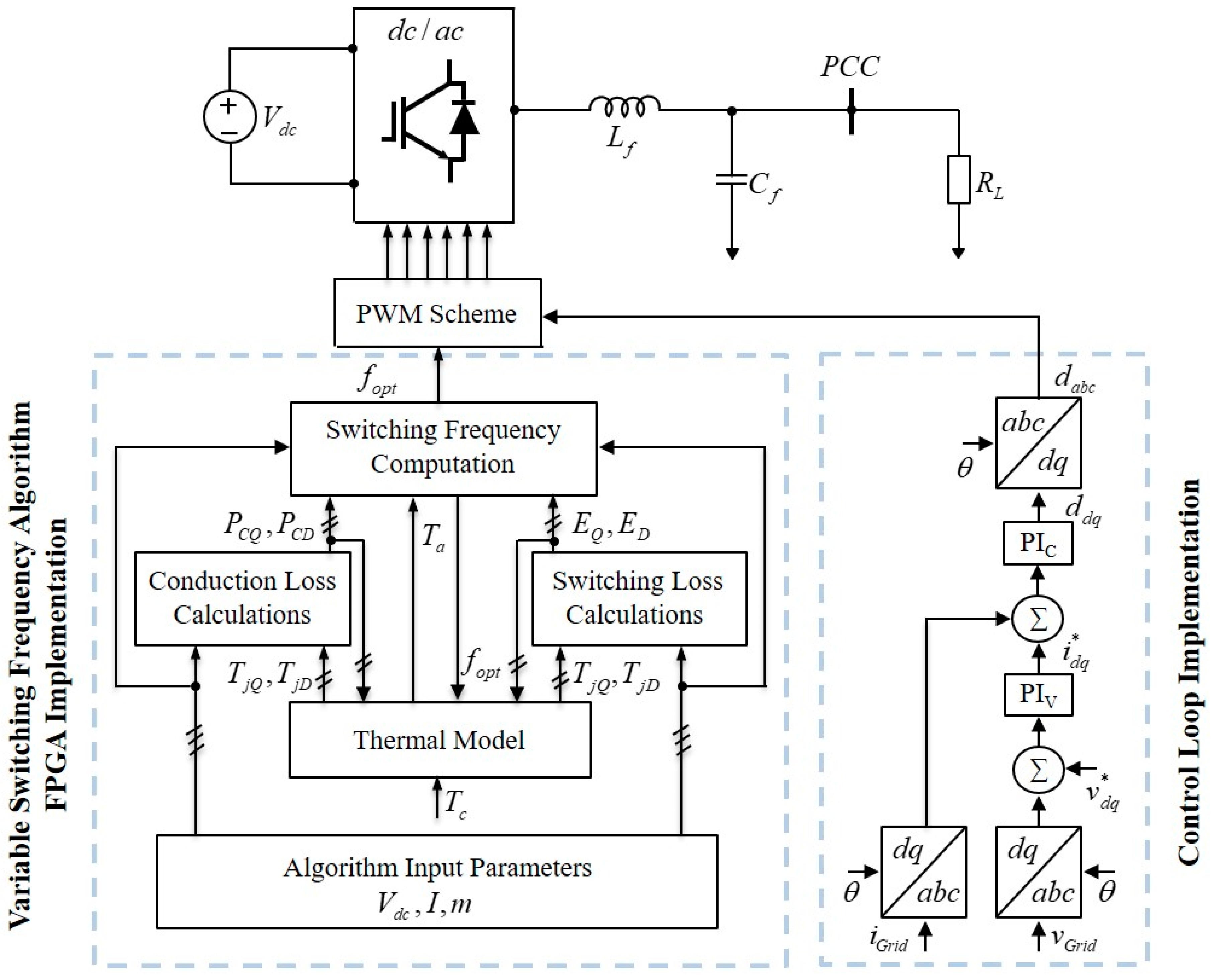
The proposed algorithm is not limited to one topology or control mode from the aforementioned architectures. However, for the sake of discussion and clarity, the grid-forming scheme is taken as an example in this paper. 
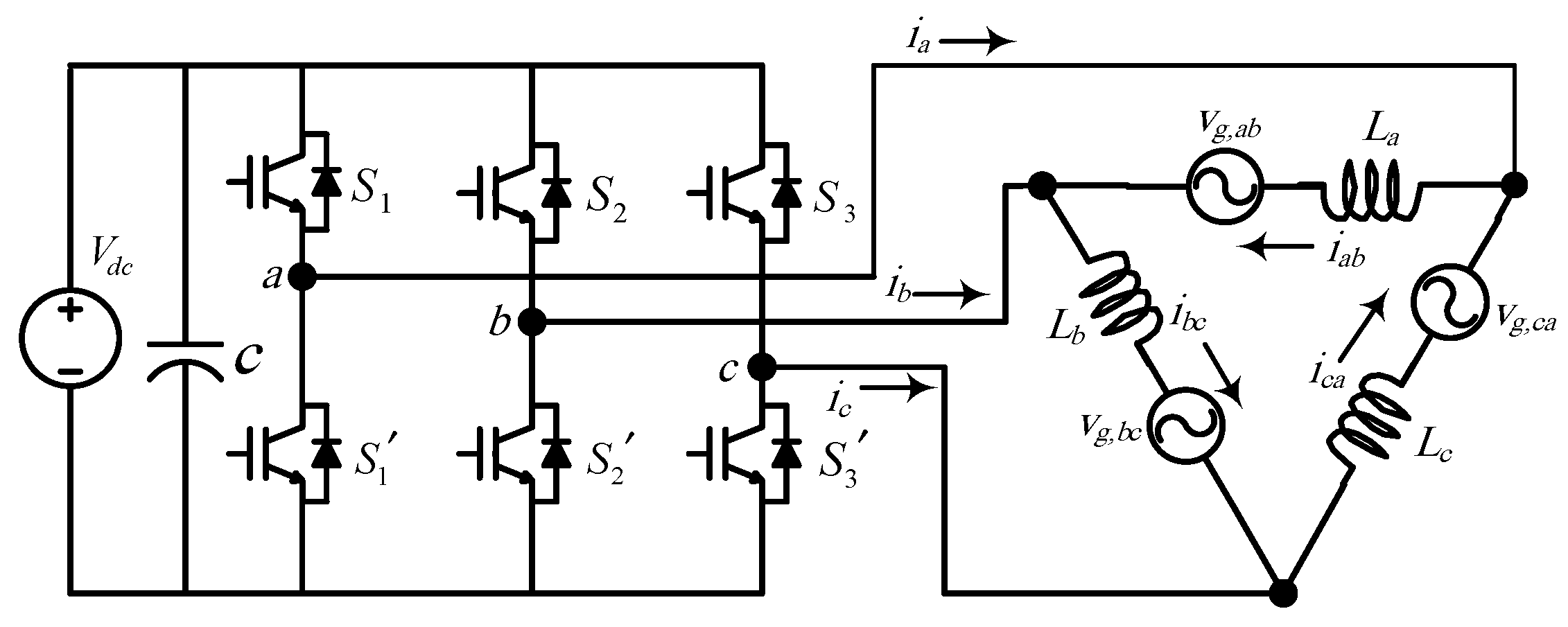
Figure 1 shows the grid-forming scheme associated with the proposed algorithm, as executed in the FPGA, which will be discussed in detail throughout the paper. To this end, any control scheme ends by generating the power reference to the pulse width modulator. The second and the important side for the modulator is generating the carrier signal and the switching frequency that are related to the proposed work. The inputs of the VSF algorithm are the loading measurements and the measured temperature.

3. Estimation of Power Losses in IGBT Power Modules

Basically, the occurrence of power losses in the inverters must be appropriately dissipated to prevent system malfunction because of overheating. The design of the cooling systems, which take responsibility for the dissipation of power losses should be optimized to prevent system failure due to insufficient design or higher costs due to overestimation. The power losses rely on the utilized modulation scheme, loading conditions and the used semiconductor switch. The behavioral model alongside loss parameters taken from the device datasheet has been adopted in this paper due to its simplicity as in [24]. Moreover, in [25,26], the adopted behavioral model provides a good estimate of the actual losses as can be deduced from their comparative analysis.
Furthermore, the antiparallel diode and IGBT encounter power losses, which include driving losses and blocking losses. These losses tend to be insignificant and can be ignored [27]; the diode turn-on losses can be ignored as well [28]. Therefore, significant power losses are usually caused by: (i) the conduction losses [26,29], (ii) the switching losses (IGBT turn on and off losses), (iii) and the diode turn-off losses (the reverse recovery losses). A typical inverter module datasheet is comprised of valuable information regarding switching and conduction losses of its specific IGBT and diode. The datasheet information will be utilized for the estimation of the significant power losses that occur in the inverter, which will be further discussed and derived in detail in the subsections that follow.

3.1. Conduction Losses

The on-state voltage of IGBT (VCE) varies with the collector current as depicted from the device voltage–current (V–I) curves at different junction temperatures (Tj) as shown in Figure 2. Due to this, it is possible to find the IGBT’s on-state voltage as a function of the collector current. Moreover, the IGBT’s on-state voltage relies on the on-state resistance (RCE), including the threshold voltage of the IGBT (VCE0). In Figure 3, RCE is the reciprocal of the slope connecting points 1 and 2 of the linearized V–I curve while VCE0 is the extrapolation of this curve to the voltage-axis. Meanwhile, the on-state resistance and the threshold voltage are temperature dependent, and, hence, this dependency should be considered. This can be achieved by interpolating RCE and VCE0 for a given junction temperature as in Equations (1) and (2) and Figure 4:
R C E ( T j ) = 5.82 × 10 7 T j 2 3.07 × 10 5 T j + 2.38 × 10 2 ,
V C E 0 ( T j ) = 9.10 × 10 6 T j 2 + 22.76 × 10 5 T j + 71.54 × 10 2 .
As a result, an approximation of the IGBT on-state voltage can be given as
V C E ( t ) = V C E 0 + R C E i c ( t ) ,
where i c ( t ) = i p k sin ( ω t ) is the phase-current that flows through the entire IGBT while conducting, i p k ( t ) is the output phase current peak value and ω is the angular frequency in rad/s.
To estimate the average conduction losses of the IGBT for one fundamental phase–current period (PCQ), the average losses in each switching period (Tsw) are lumped together, and then divided by the total number of the switching pulses as
P C Q = 1 N n 1 T s w ( n 1 ) T s w n T s w i c ( t ) V C E ( t ) d t ,
where N is considered as the total sum of pulses for each fundamental period and n is the switching pulse index.
In a case whereby fsw is highly relative to the fundamental frequency, which is the typical case for SPWM inverter, it is possible to assume that the collector current is constant during every Tsw, that is,
i c ( ( n 1 ) T s w ) i c ( n T s w ) .
The IGBT is conducting for D n T s w at the nth switching cycle, where D n is the duty cycle of the voltage pulses. Therefore, Equation (4) can be rewritten as
P C Q = 1 N n 1 T s w ( n 1 ) T s w ( n 1 + D n ) T s w i c ( t ) V C E ( t ) d t .
Taking Equations (3) and (5) into account, and evaluating the integral in Equation (6) yields
P C Q = 1 N n 1 T s w i c ( n T s w ) [ V C E 0 + R C E i c ( n T s w ) ] D n T s w .
For the summation given in Equation (7), integration can be used to approximate it considering the assumption of fsw is much higher than the fundamental frequency, and this assumption will be used throughout this study. Subsequently, the current flows through the IGBT at half period when its antiparallel diode is not conducting, and the integration is evaluated over half of the fundamental period ( T ) as in Equation (8):
P C Q 1 T 0 T / 2 i c ( t ) [ V C E 0 + R C E   i c ( t ) ] D ( t ) d t .
For SPWM modulation, the duty cycle as a function of time can be written as in Equation (9) [24]:
D ( t ) = 1 + m sin ( ω t + θ ) 2 ,
where θ is considered as the angle difference between the output phase current and output phase voltage in radian and m is the modulation index. Then, an evaluation of the integral yields:
P C Q = V C E 0   i p k 2 π + R C E i p k 2 8 + ( V C E 0 i p k 8 + R C E i p k 2 3 π ) m   cos ( θ ) .
The same procedure used to compute the IGBT conduction losses will be used to compute the conduction losses of the antiparallel diode as well. A linear approximation of the V–I characteristics of the diode can be given as
V f ( t ) = R f   i f ( t ) + V f 0 ,
where V f 0 is the threshold voltage of the diode and R f is the forward resistance of the diode. The dependency of V f 0 and R f on the junction temperature is expressed in Figure 5 and Equations (12) and (13):
R f ( T j ) = 4.16 × 10 8 T j 2 + 5.27 × 10 6 T j + 2.14 × 10 2 ,
V f 0 ( T j ) = 9.22 × 10 6 T j 2 39.76 × 10 5 T j + 86.91 × 10 2 .
The diode is conducting for ( 1 D n ) T s w at the nth switching cycle. Taking this into consideration and following the same adopted procedure in deriving the conduction losses in the IGBT, the diode conduction losses can be written as in Equation (14):
P C D = V f 0   i p k 2 π + R f i p k 2 8 ( V f 0 i p k 8 + R f i p k 2 3 π ) m   cos ( θ ) .

3.2. Switching Losses

The turn-on and off energy losses for every Tsw are provided in the device datasheet. Those are losses that rely substantially on the collector current ( i c ), the IGBT’s junction temperature ( T j Q ), DC-link voltage ( V d c ), and turn-on ( R g , o n ) and turn-off ( R g , o f f ) gate resistances. For all the previous dependencies to be considered, 3D-curve fitting techniques are used for energy losses to be expressed based on the parameters above. With the use of the surface fitting, the turn-on and the turn-off energy losses ( E o n and E o f f ) are expressed in terms of i c and T j Q , as shown in Figure 6 and Equations (15) and (16). After that, the derived equations must be scaled to include the effect of a specific R g , o n , R g , o f f and V d c as in Equations (17) and (18):
E o n ( i c , T j ) = 30.34 × 10 3 i c + 75.79 × 10 6 i c 2 + 1.2 × 10 4 i c T j ,
E o f f ( i c , T j ) = 46.92 × 10 3 i c 3.939 × 10 4 i c 2 + 6 × 10 5 i c T j ,
E o n = V d c V d c , t e s t E o n ( R g , o n ) E o n ( R g , o n , t e s t ) E o n ( i c , T j Q ) ,
E o f f = V d c V d c , t e s t E o f f ( R g , o f f ) E o f f ( R g , o f f , t e s t ) E o f f ( i c , T j Q )   .
The notation ‘test’ represents the value that is utilized in the measurements of the energy losses test. Based on Equations (17) and (18), the average losses due to switching for every fundamental period ( P s w Q ) are given as in Equation (19):
P s w Q = 1 N T n ( E o n + E o f f ) .
In Equation (19), E o n and E o f f are functions of the collector current ( i c ( t ) = i p k sin ( ω t ) ). Based on estimation, it is assumed that the switching power losses are sinusoidal, while Equations (17) and (18) define the sine function peak of E o n and E o f f , respectively, at the peak evaluation of the collector current. An approximation of the summation in Equation (19) can be given by the integration as in Equation (20):
P s w Q = 1 T [ ( E o n + E o f f ) f s w ] 0 T / 2 sin ( ω t ) d t = E o n + E o f f π f s w .

3.3. Reverse Recovery Losses

Following the same procedure in Section 3.2 but for the diode, Figure 7 shows the reverse recovery energy losses as functions of i f and T j and Equation (21) is the corresponding 3D-curve fitted equation:
E r e c ( i f , T j ) = 20.64 × 10 3 i f 4.827 × 10 4 i f 2 + 7 × 10 5 i f T j .
As a result, the formulations for the reverse recovery losses are expressed as:
E r e c = V d c V d c , t e s t E r e c ( R g , o n ) E r e c ( R g , o n , t e s t ) E r e c ( i f , T j )   ,
P s w D = E r e c π f s w .
The total IGBT module power losses can be finally formulated as in Equation (24):
P T = 6 ( P C Q + P C D + P s w Q + P s w D ) .

4. Thermal Modeling of the IGBT Power Module

Power losses that occur in a semiconductor switch are the main cause of rise of its junction temperature; therefore, a thermal model that estimates the junction temperature from the power losses has to be constructed. Thermal models can be steady-state models such as thermal resistance networks in which only the steady-state temperatures can be estimated, or dynamic models such as the well-known Foster and Cauer models that can estimate the transient behavior of the temperature when it changes from one steady-state point to another [31]. For gird-tied inverters, the time interval between two consecutive active-power set-points is much larger than the time constant of the thermal model in general. Since the aim of this study is to develop an algorithm that changes the switching frequency with the change in the steady-state operating conditions (mainly the active-power) as will be described later, thermal transients can be ignored. Hence, a steady-state thermal model is adopted in this study. In steady-state operating conditions, a specific IGBT conducts for a half-cycle, whereas its anti-parallel diode conducts for the other half, which causes the junction temperature to increase during the half-cycle of conduction and decrease during the other one; this causes a junction temperature ripple that the steady-state thermal model cannot estimate. However, for 50–60 Hz operation, the junction temperature ripple is much smaller than the average value of the junction temperature; therefore, a steady-state thermal model can be used. To account for the rise of the instantaneous junction temperature above its average value, the maximum junction temperature that corresponds to the maximum power dissipation is set to a value lower than the maximum operating junction temperature defined in the datasheet of the semiconductor device; this practice is a norm when it comes to the design of cooling systems of semiconductors.
Using the analogy between the electrical and thermal systems, it becomes possible to construct a thermal network whereby each resistor represents the thermal resistance regarding a particular material or path, while each current source represents a source of power loss. Moreover, the temperature difference across a particular material is represented by the voltage difference across the resistor [32].
The thermal resistance of a material in °C/W is defined as its resistance to heat flow across a temperature gradient. In the datasheet of the IGBT modules, the thermal resistances (Rx) of the major heat flow paths are provided, the notation ‘x’ can be {j,C,S,A} to denote the junction, case, sink and ambient, respectively. In addition, the zero-order thermal resistance network [26] of the IGBT module shown in Figure 8, is adopted in this study. This thermal model matches the fast-computational time associated with the proposed online variable switching frequency algorithms. The thermal resistance of the heat sink is denoted as ( R S A ). Based on Figure 8, the following relations can be deduced:
T s = 6 ( P Q + P D ) R S A + T a ,
T c = 6 ( P Q + P D ) R C S + T s ,
T j Q = P Q   R j C Q + T c ,
T j D = P l o s s , D   R j C D + T c ,
where T s is the heat sink temperature, T a is the ambient temperature, T c is the case (or base-plates), T j Q is the IGBT’s junction temperature, and T j D is the diode’s junction temperature. All the temperatures are in °C.

5. Time Domain Current Ripple Analysis

Figure 9 shows the circuit diagram of the grid connected inverter, which includes an inductor ( L ) to represent the grid-inductance in series with a sinusoidal voltage source ( v g ) for the grid to be represented. This representation is valid for any inverter that supplies motor loads and/or grids [33].
Before proceeding with the current-ripple analysis based on time domain, the following assumptions are made:
  • The input voltage is ripple-free.
  • fsw is relatively higher compared to the fundamental frequency.
  • The modulating signals during each Tsw remain constant.
  • The impact of dead-time is neglected.
From the circuit diagram of Figure 9, the voltage between phases a and b can be written as
v a b = v g , a b + L d i a b d t ,
where v a b is the inverter’s output line-line voltage, i a b is the phase-current, and v g , a b is the line-line grid voltage.
As mentioned earlier, the load current consists of the ripple component and the fundamental-frequency component. Therefore, i a b can be written as
i a b = i ¯ a b + i ^ a b ,
where i ¯ a b is the load current fundamental component and i ^ a b is the load current ripple component. Substituting Equation (30) in Equation (29), yields Equation (31), and then the load current ripple component can be expressed as in Equation (32):
v a b = v g , a b + L ( d i ¯ a b d t + i ^ a b d t ) ,
i ^ a b = v a b v g , a b L d t .
The term d i ¯ a b / d t doesn’t appear in Equation (32) because of the assumption that the fundamental component is constant within Tsw. The inductor resistance can be neglected, and since fsw is much greater compared to the fundamental frequency, the current ripple component is placed under the assumption of rising and falling in a linear manner around the fundamental value. Using linear approximation, each segment of the current ripple is given as
i ^ a b = t 2 t 1 L ( v t 2 v t 1 ) ,
where i ^ a b is the current ripple segment over the interval of time ( t 2 t 1 ) , v t 1 is the voltage at time t 1 and v t 2 is the voltage at time t 2 .
The ripple component and the output line-line voltage of the load current at Tsw are shown in Figure 10. The ripple of the load current can be given as
i ^ a b = t t 0 L v g , a b ;   for   t 0 t t 1 ,
i ^ a b = T 0 L v g , a b + t t 1 L ( V d c v g , a b ) ;   for   t 1 t t 3 ,
i ^ a b = t t 4 L v g , a b + T 1 + T 2 L ( V d c v g , a b ) T 0 L v g , a b ;   for   t 3 t t 4 .
The ripple current mean square value over Tsw (i.e., I ^ a b 2 ) can be expressed as
I ^ a b 2 = 2 f s w t 0 t 0 + t 4 i ^ a b 2 d t = 2 V d c 2 f s w L 2 { 0 T 0 t 2 d t + 0 T 3 t 2 d t + 0 T 1 + T 2 [ T 0 + ( V d c v g , a b 1 ) t ] 2 d t } ,
I ^ a b 2 = 2 V d c 2 f s w L 2 [ T 0 3 3 + T 0 2 ( T 1 + T 2 ) ( V d c v g , a b 1 ) T 0 ( T 1 + T 2 ) 2 + ( V d c v g , a b 1 ) 2 ( T 1 + T 2 ) 3 3 + T 3 3 3 ] .
The time intervals T 0 , T 1 , T 2 and T 3 can be related to T s w as
T 0 = ( 1 4 1 4 f 1 ( t ) ) T s w ,
T 1 = ( f 1 ( t ) f 1 ( t ) 4 ) T s w ,
T 2 = ( f 3 ( t ) f 2 ( t ) 4 ) T s w ,
T 3 = ( 1 4 + 1 4 f 1 ( t ) ) T s w ,
f 1 ( t ) = m sin ( ω t ) ;   f 2 ( t ) = m sin ( ω t + 2 π 3 ) ;   f 3 ( t ) = m sin ( ω t + 4 π 3 ) .
Substituting Equation (43) in Equations (40), (41), and (42) yields
I ^ a b 2 = ( V d c L f s w ) 2 m 2 64 sin 2 ( 2 π f t + π 6 ) × [ 1 3 m sin ( 2 π f t + π 6 ) + 3 4 m 2 ] .
To find the current ripple root mean square (rms) value over a fundamental period ( I ^ h , r m s ), Equation (44) is integrated over the fundamental period as in Equation (45):
I ^ h , r m s = 1 π π / 6 5 π / 6 I ^ a b 2   d ω t .
It should be noted that the integration was conducted over the period [ π / 6 , 5 π / 6 ] and the symmetry justifies integration over a half period. Substituting Equation (44) in Equation (45) gives
I ^ h , r m s = m V d c 16 L f s w 2 16 3 3 π m + 3 2 m 2 .
If it is a Y-connected load, Equation (46) yields
I ^ h , r m s = m V d c 16 3 L f s w 2 16 3 3 π m + 3 2 m 2 .
The THD in the inductor current T H D i is given as
T H D i = I ^ h , r m s I ¯ a b , r m s ,
where I ¯ a b , r m s is the fundamental current’s rms value.

6. The Proposed VSF Algorithm

Generally, the manufacturers of grid-tied inverters specify the PWM switching frequency fsw as a design value with respect to the rated operating conditions. Increasing fsw reduces the rms value of the current ripple and therefore the total demand distortion TDD is reduced as well. However, the value of fsw is limited by the heat dissipation capability of the semiconductor power switches and their associated cooling system. When the operating point of the inverter is below the rated conditions, the cooling system appears to be oversized since it is possible to increase the switching frequency and hence enhance the quality of the output current. Using the aforementioned premise, each operating condition can be considered as a design problem; however, the switching frequency is the only degree of freedom that is available in the problem design. Therefore, an algorithm that is able to improve the output power quality of the grid-tied inverter without changing the physical structure of the system is significant from an industrial point of view [34].
Increasing fsw will increase the power losses and hence reduce the efficiency. However, the output power quality is improved. Since increasing or decreasing fsw will improve one feature of the system and degrade the other, this means that a conflict between two desired objectives is met, which is a typical multi-objective optimization problem. In such problems, there is no unique optimal solution but rather a set (maybe infinite) of optimal solutions. The selection of one solution among the set of solutions is a degree of freedom left to the preference of the designer [35,36].
To obtain an optimal solution with a reduced computational complexity that is strictly required for an algorithm that can determine the optimal fsw online (i.e., without heavy offline calculations that are stored in lookup tables), a weighted-sum objective function is defined as follows:
M i n             Ψ ( f s w ) = ( 1 w )   × T D D   ( f s w ) + w ×   P s w ( f s w ) ,
where Ψ is the optimization cost function to be minimized. fsw is bounded by the upper and the lower permissible bounds, fsw,l and fsw,u, respectively. w [ 0 1 ] is the trade-off factor. To this end, since each individual goal has distinct value, it is advisable to normalize both objectives in order to avoid misleading solutions as
Ψ n = w P s w , t o t a l P s w , t o t a l i d e a l P s w , t o t a l n a d i r P s w , t o t a l i d e a l + ( 1 w ) T D D T D D i d e a l T D D n a d i r T D D i d e a l ,
where Ψ n is the normalized cost function, T D D i d e a l is the TDD at f s w , u , T D D n a d i r is the TDD at f s w , l , P s w , t o t a l i d e a l is the least expected switching losses, and P s w , t o t a l n a d i r is the highest acceptable switching losses.
Furthermore, the optimal value of fsw ( f s w o p t ) can be found by equating the first order derivative of Equation (50) to zero, that is:
d Ψ n d f s w = w 1 f s w , u f s w , l ( 1 w ) f s w , u f s w , l f s w , u f s w , l 1 f s w 2 = 0 .
Rearranging Equation (51) yields
f s w o p t = 1 w w f s w , l × f s w , u .
As the operation and the loading conditions are varying, there is a change in the energy losses. Therefore, f s w , u changes. In other words, for every new condition that emerges, a new optimization problem is solved. The maximum allowable switching frequency ( f s w , u ) can be expressed based on switching energy losses given in Equation (53). However, f s w , l is restricted by the highest allowable T D D , which is assumed to be 5%. The minimum allowable switching frequency can be expressed as in Equation (54):
f s w , u = π   P s w , t o t a l n a d i r 6 ( o n + E o f f + E r e c ) ,
f s w , l = ( m V d c 16 3 L 2 16 3 3 π m + 3 2 m 2 1 I L , r m s r a t e d ) 1 0.05 .
Making use of Equations (53) and (54), (52) can be rewritten as
f s w o p t = 1 0.05 ( m V d c 16 3 L 2 16 3 3 π m + 3 2 m 2 1 I L , r m s r a t e d )   × π   P s w , t o t a l n a d i r 6   ( o n + E o f f + E r e c ) × 1 w w .
The highest permissible losses are limited by the highest allowable TJQ and TJD. This value has to be evaluated for each new ambient temperature. Based on the thermal layout in Figure 8, the highest permissible total losses for each diode ( P D max ) at a given ambient temperature can be given as in Equation (56) and the highest permissible losses for each IGBT ( P Q max ) can be related to Equation (56) as shown in Equation (57):
P D max = T j D , max T a R J C D + 6   ( R C S + R S A + R j C D R j C Q ( R C S + R S A ) ) ,
P Q max = R j C D R j C Q P D max .
From Equations (56) and (57), the highest permissible losses ( P s w , t o t a l n a d i r ) can be evaluated with a consideration of just the switching loss aspect as follows:
P s w , t o t a l n a d i r = 6   ( P D max   ( 1 + R j C D R j C Q ) P C D P C Q ) .
Figure 1 shows the implementation of the proposed algorithm in the FPGA platform. The operating conditions including the modulation index, the DC-link voltage, and grid current, and the power factor are used to estimate the conductions losses utilizing Equations (10) and (14) and the energy switching losses evaluating Equations (17), (18) and (22). From the power and energy losses’ estimates, the optimal switching frequency is computed from Equation (55). Since the junction temperatures and power losses are mutually dependent, an iterative solution must be used as in Figure 11. It should be mentioned that the effect of the ambient temperature is taken into consideration as feedback from the case temperature, since the IGBT power module includes a thermistor that can be measured as in Figure 1.

7. The Experimental Results

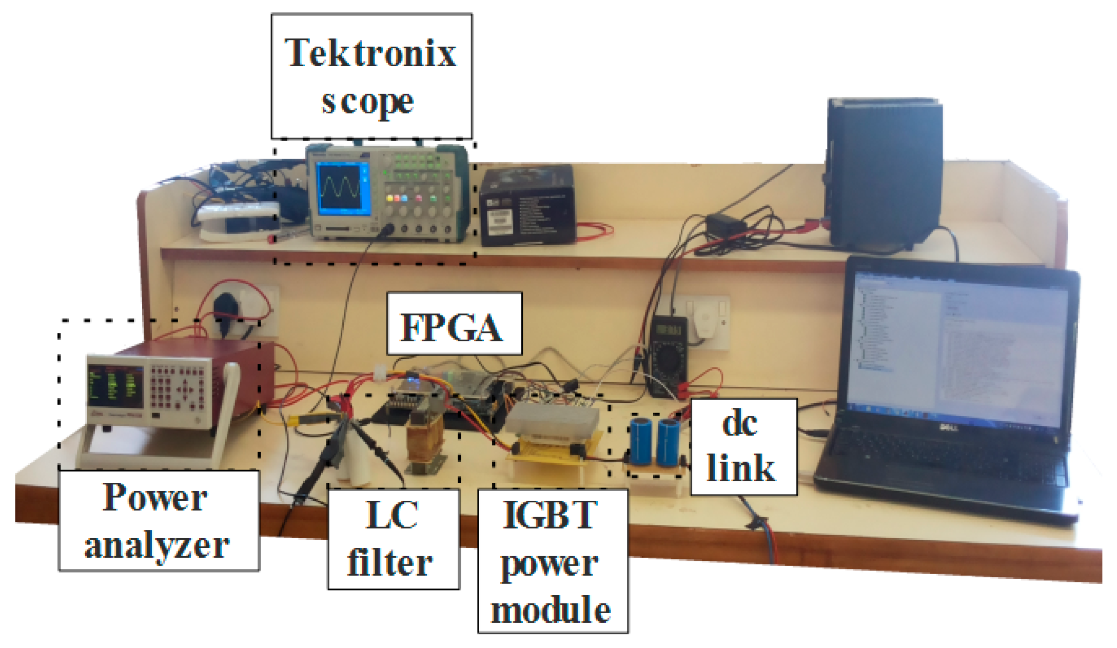
Validating the significance of this proposed algorithm requires the setup of an experiment as in Figure 12. The experimental tests were performed on three-phase IGBT power module (Part Number: FP50R06KE3) cascaded with passive low pass inductor and capacitor (LC) filter output and supplying a Y-connected resistive load. Table 1 illustrates the system parameters and Table 2 depicts the optimal switching frequency at different loading conditions alongside total switching losses, TDD, and case temperature assuming a weighting factor of 0.6. As is evident, the proposed algorithm varies fsw to obtain the best balance between the TDD and the switching losses based on inverter’s loading conditions including the ambient temperature. When this system is at heavy loads, switching losses are high; therefore, the algorithm reduces fsw, while keeping the TDD below the 5% limit (IEEE standard 519-2014). However, at light loads, the switching losses becomes low; hence, the algorithm increases the switching frequency for the output current quality to be enhanced.
The measurement of the TDD was carried out by measuring the total harmonic distortion of the output current ( T H D i ) at certain loading conditions using the harmonic analysis functionality provided by a Tektronix oscilloscope (Model Number: TPS2024B). According to IEEE-519 TDD is defined as “the total root-sum-square harmonic current distortion, in percent of the maximum demand load current”. The calculated TDD is obtained from T H D i , the rms value of load current ( i r m s ) and the rms value of the rated current ( i r m s r a t e d ) as in Equation (59)
T D D = T H D i i r m s i r m s r a t e d .
The measurement of the switching losses is initiated by measuring the steady-state case temperature at each operating condition by which the total power losses can be estimated. To extract the switching losses component, the experiment is performed again with fixed switching frequency while keeping other operating conditions unchanged, and, as a result, the conduction losses are unchanged as well. Since the switching losses are almost linearly related to the switching frequency, the switching losses can be deduced.
The following steps describe the experimental procedure in which switching losses are extracted:
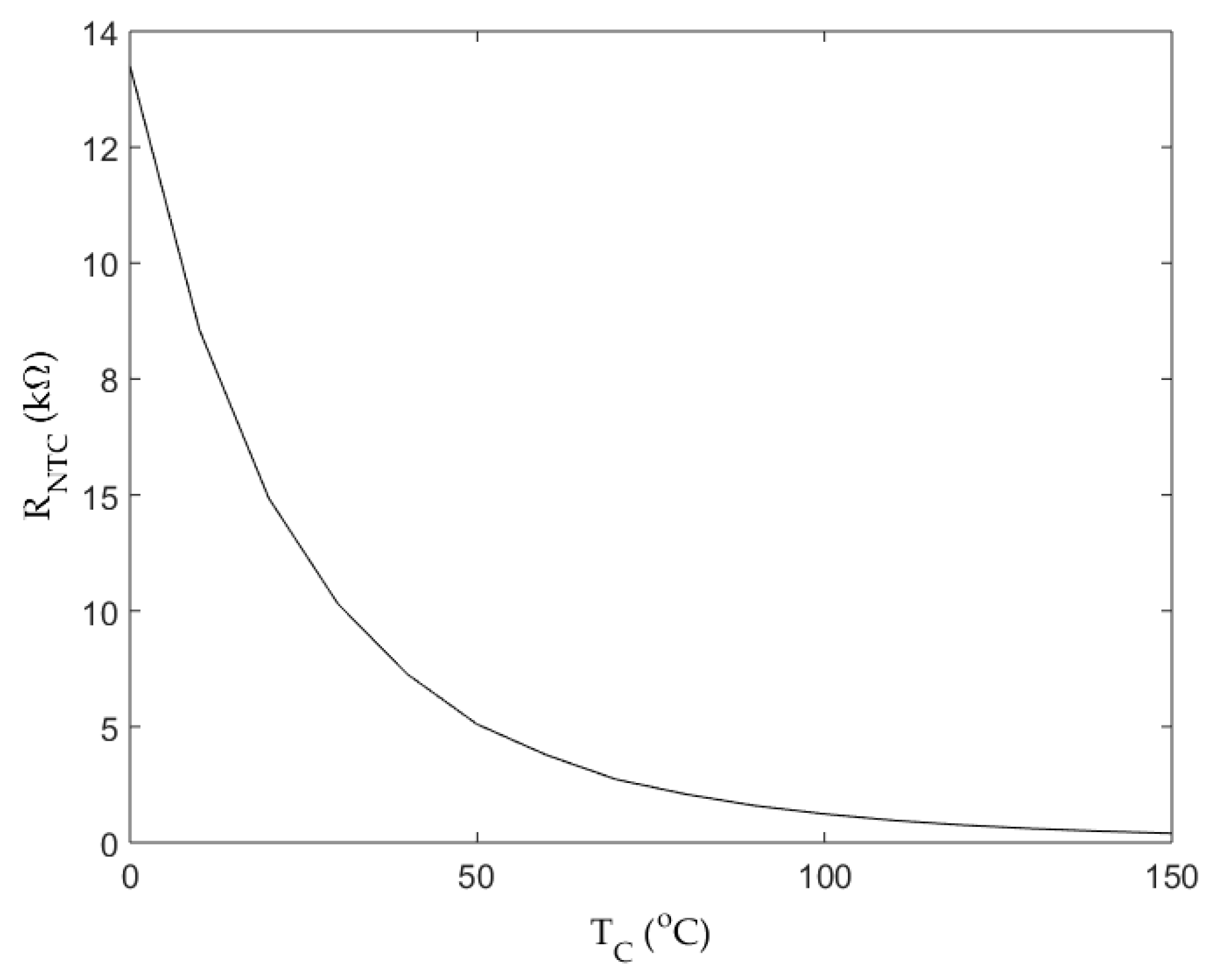
(1)
Measure the case (base plate) temperature by the solid state temperature sensors (negative temperature coefficient (NTC) thermistor) RNTC. The temperature characteristic of this thermistor is shown in Figure 13 and Equation (60):
T c = 26.48 R N T C 2 + 346.9 R N T C + 211.4 R N T C 2 + 5.345 R N T C + 0.9036 .
(2)
From the measured case temperature and based on re-arranging of Equations (24)–(28), the total power losses is determined by Equation (61)
P T = T c T a R S A + R C S .
(3)
Under the same loading conditions, the switching frequency is varied, case temperature is measured, and losses are calculated.
(4)
Based on the calculated power losses, the following set of Equations (62)–(65) can be computed:
P T ( f s w 1 ) = P C Q + P C D + E o n + E o f f + E r e c π f s w 1 ,
P T ( f s w 2 ) = P C Q + P C D + E o n + E o f f + E r e c π f s w 2 ,
P T ( f s w 2 ) P T ( f s w 2 ) = E o n + E o f f + E r e c π ( f s w 2 f s w 1 ) ,
P T = P T ( f s w 2 ) P T ( f s w 2 ) f s w 2 f s w 1 f s w 1 ,
where f s w 1 is the switching frequency of interest and f s w 2 is the second switching frequency.
Validating how effective the proposed algorithm requires the experimental system to be tested with a fixed fsw while constantly keeping the TDD at 2.5%. fsw is selected as 25 kHz, which is approximately the middle point relative to the variable frequency range, with the system being tested under the same load conditions. Table 3 summarizes the performance of the inverter. Comparing the results from Table 3 and Table 4, there is a reduction of the switching power losses at full load by about 51.6% using the proposed VSF algorithm, while the TDD is below the 5% limit. The decrease in the switching losses with the use of the proposed VSF algorithm is justified by the fact that the weight of 0.6 automatically leads the algorithm to favor the reduction of the switching power losses. 
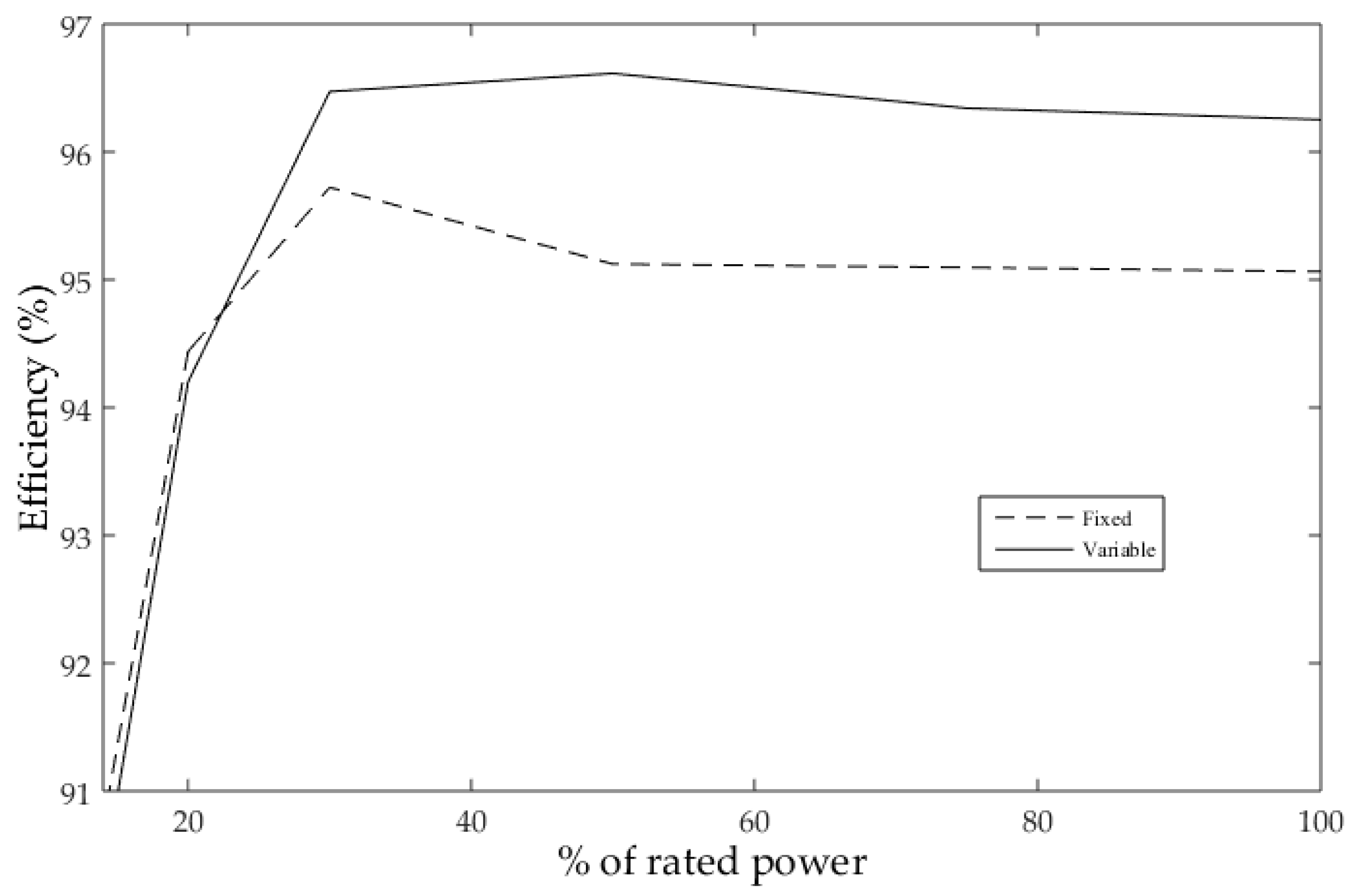
Figure 14 gives the measured efficiency curves, which is for the whole inverter system alongside the fixed and VSF algorithms. It is obvious that the inverter efficiency is enhanced for a large array of load conditions. Table 4 indicates a comparison between the calculated and experimental results. It can be shown that the power losses and TDD models are highly accurate.
To further highlight the significance of the proposed algorithm, the California Energy Commission (CEC) efficiency of the inverter is measured under the fixed and VSF algorithms, the CEC efficiency is 97.3% using the proposed VSF algorithm, and 96.39% with the fixed fsw. Therefore, it can be deduced from comparing the efficiencies of both algorithms that fsw can be increased without degrading the efficiency of the inverter.
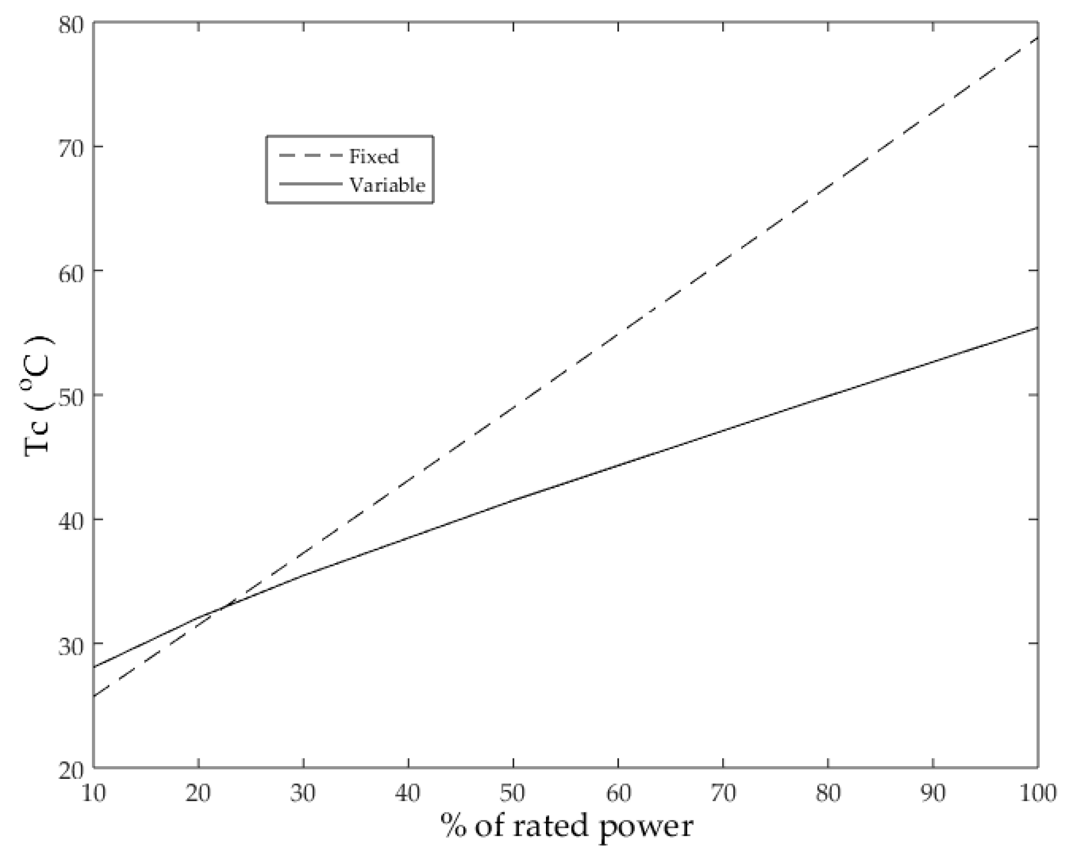
An interesting property related to the proposed VSF algorithm is the fact that the junction temperature variation under different load conditions tends to be lower than that one under fixed fsw. As can be shown in Figure 15, the case temperature rate of change with the VSF algorithm is less than that of the fixed fsw. This property holds even if more weight is given to the TDD. In other words, regardless of the selected weighting factor, the temperature profile when using the proposed algorithm will always have a slope that is under the one when using the fixed switching frequency. The importance of this property comes from the fact that the lifetime of the inverter is inversely proportional to the junction temperature difference [37,38,39].

8. Conclusions

This study achieves the development of an online adaptive switching algorithm. In this algorithm, fsw tends to be varied online according to the loading conditions and the ambient temperature. Depending on the models developed in Section 2 and Section 3, fsw was expressed based on the operating conditions, and an optimization issue was created using the multi-objective optimization theory. It was shown that the algorithm increases over all the inverter’s efficiency from 96.39% to 97.3% at full load without degrading the output power quality. The inverter’s lifetime can be increased because of the limited case temperature rate of change as well. The implementation of the developed algorithm is straightforward and the optimization can be performed online without complex computations, by which the intensive offline calculations and lookup tables are totally avoided.

Acknowledgments

Besides the open access fees, this research was supported by the deanship of research at Jordan University of Science and Technology (Grant number: 20150010).

Author Contributions

S.A. and H.J.A. designed the research idea and the experimental setup. I.A.S. and A.K. updated the literature review and improved the quality of presentation. I.A.S. and A.K. reviewed the estimation of power loses equations in IGBT power module. I.A.S. and H.J.A. analyzed the results. A.K. and S.A. did the graphical work. All authors participated in providing answers to all comments from reviewers. All authors read and approved the final manuscript.

Conflicts of Interest

The authors declare no conflict of interest.

References

  1. Chen, M.-H. Use of Three-Level Power Converters in Wind-Driven Permanent-Magnet Synchronous Generators with Unbalanced Loads. Electronics 2015, 4, 339–358. [Google Scholar] [CrossRef]
  2. Al-Hoor, W.; Abu-Qahouq, J.A.; Huang, L.; Mikhael, W.B.; Batarseh, I. Adaptive Digital Controller and Design Considerations for a Variable Switching Frequency Voltage Regulator. IEEE Trans. Power Electron. 2009, 24, 2589–2602. [Google Scholar] [CrossRef]
  3. He, X.F.; Zhang, Z.; Cai, Y.Y.; Liu, Y.F. A variable switching frequency hybrid control for ZVS dual active bridge converters to achieve high efficiency in wide load range. In Proceedings of the 29th Annual IEEE Applied Power Electronics Conference and Exposition (APEC), Fort Worth, TX, USA, 16–20 March 2014; pp. 1095–1099. [Google Scholar]
  4. Arikatla, V.; Qahouq, J.A.A. Dynamic digital variable switching frequency control scheme for power converters. In Proceedings of the 26th Annual IEEE Applied Power Electronics Conference and Exposition (APEC), Fort Worth, TX, USA, 6–10 March 2011; pp. 253–257. [Google Scholar]
  5. Kumar, A.C.B.; Narayanan, G. Variable switching frequency PWM technique for induction motor drive to spread acoustic noise spectrum with reduced current ripple. IEEE Trans. Ind. Appl. 2014, 52, 1–6. [Google Scholar] [CrossRef]
  6. Jiang, D.; Wang, F. Variable Switching Frequency PWM for Three-Phase Converters Based on Current Ripple Prediction. IEEE Trans. Power Electron. 2013, 28, 4951–4961. [Google Scholar] [CrossRef]
  7. Yang, F.; Taylor, A.R.; Bai, H.; Cheng, B.; Khan, A.A.; Lee, Y.J.; Nie, Z. Application of variable switching frequency PWM control with power loss prediction in surfaced-mounted permanent magnet synchronous motor. In Proceedings of the Transportation Electrification Asia-Pacific (ITEC Asia-Pacific), Beijing, China, 31 August–3 September 2014; pp. 1–4. [Google Scholar]
  8. Yang, F.; Taylor, A.R.; Bai, H.; Cheng, B.; Khan, A.A. Using d–q Transformation to Vary the Switching Frequency for Interior Permanent Magnet Synchronous Motor Drive Systems. IEEE Trans. Transp. Electrif. 2015, 1, 277–286. [Google Scholar] [CrossRef]
  9. Mao, X.; Ayyanar, R.; Krishnamurthy, H.K. Optimal Variable Switching Frequency Scheme for Reducing Switching Loss in Single-Phase Inverters Based on Time-Domain Ripple Analysis. IEEE Trans. Power Electron. 2009, 24, 991–1001. [Google Scholar]
  10. Cao, B.; Chang, L. A variable switching frequency algorithm to improve the total efficiency of single-phase grid-connected inverters. In Proceedings of the 28th Annual IEEE Applied Power Electronics Conference and Exposition (APEC), Long Beach, CA, USA, 17–21 March 2013; pp. 2310–2315. [Google Scholar]
  11. Andersson, A.; Thiringer, T. Inverter losses minimization using variable switching frequency based on multi-objective optimization. In Proceedings of the International Conference on Electrical Machines (ICEM), Berlin, Germany, 2–5 September 2014; pp. 789–795. [Google Scholar]
  12. Cao, W.; Wang, F.; Jiang, D. Variable switching frequency PWM strategy for inverter switching loss and system noise reduction in electric/hybrid vehicle motor drives. In Proceedings of the Applied Power Electronics Conference and Exposition (APEC), Long Beach, CA, USA, 17–21 March 2013; pp. 773–780. [Google Scholar]
  13. Anuchin, A.; Gulyaeva, M.; Briz, F.; Gulyaev, I. Modeling of AC voltage source inverter with dead-time and voltage drop compensation for DPWM with switching losses minimization. In Proceedings of the International Conference on Modern Power Systems (MPS), Cluj-Napoca, Romania, 6–9 June 2017; pp. 1–6. [Google Scholar]
  14. Abdelhakim, A.; Davari, P.; Blaabjerg, F.; Mattavelli, P. Switching Loss Reduction in the Three-Phase Quasi-Z-Source Inverters Utilizing Modified Space Vector Modulation Strategies. IEEE Trans. Power Electron. 2017. [Google Scholar] [CrossRef]
  15. Oñederra, O.; Kortabarria, I.; de Alegría, I.M.; Andreu, J.; Gárate, J.I. Three-Phase VSI Optimal Switching Loss Reduction Using Variable Switching Frequency. IEEE Trans. Power Electron. 2017, 32, 6570–6576. [Google Scholar] [CrossRef]
  16. Bhattacharya, S.; Sharma, S.K.; Mascarella, D.; Joós, G. Subfundamental Cycle Switching Frequency Variation for Switching Losses Reduction of a Two-Level Inverter Traction Drive. IEEE Trans. Transp. Electrif. 2017, 3, 646–655. [Google Scholar] [CrossRef]
  17. Charumit, C.; Kinnares, V. Discontinuous SVPWM Techniques of Three-Leg VSI-Fed Balanced Two-Phase Loads for Reduced Switching Losses and Current Ripple. IEEE Trans. Power Electron. 2015, 30, 2191–2204. [Google Scholar] [CrossRef]
  18. Golwala, H.; Chudamani, R. New Three-Dimensional Space Vector-Based Switching Signal Generation Technique Without Null Vectors and With Reduced Switching Losses for a Grid-Connected Four-Leg Inverter. IEEE Trans. Power Electron. 2016, 31, 1026–1035. [Google Scholar] [CrossRef]
  19. Xia, Y.; Roy, J.; Ayyanar, R. Optimal variable switching frequency scheme for grid connected full bridge inverters with bipolar modulation scheme. In Proceedings of the IEEE Energy Conversion Congress and Exposition (ECCE), Cincinnati, OH, USA, 1–5 October 2017; pp. 4260–4266. [Google Scholar]
  20. Li, Q.; Jiang, D. Variable Switching Frequency PWM Strategy of Two-Level Rectifier for DC-link Voltage Ripple Control. IEEE Trans. Power Electron. 2017. [Google Scholar] [CrossRef]
  21. Ramirez, F.; Pacas, M. Finite Control Set Model Based Predictive Control of a PMSM with Variable Switching Frequency and Torque Ripple Optimization. In Proceedings of the PCIM Europe International Exhibition and Conference for Power Electronics, Intelligent Motion, Renewable Energy and Energy Management, Nuremberg, Germany, 10–12 May 2016; pp. 1–8. [Google Scholar]
  22. Pai, P.; Reiter, T.; Maerz, M. A New Behavioral Model for Accurate Loss Calculations in Power Semiconductors. In Proceedings of the PCIM Europe International Exhibition and Conference for Power Electronics, Intelligent Motion, Renewable Energy and Energy Management, Nuremberg, Germany, 10–12 May 2016; pp. 1–9. [Google Scholar]
  23. Rocabert, J.; Luna, A.; Blaabjerg, F.; Rodríguez, P. Control of Power Converters in AC Microgrids. IEEE Trans. Power Electron. 2012, 27, 4734–4749. [Google Scholar] [CrossRef]
  24. You, K.; Rahman, M.F. Analytical Model of Conduction and Switching Losses of Matrix-Z-Source Converter. J. Power Electron. 2009, 9, 275–287. [Google Scholar]
  25. Reichl, J.; Lai, J.S.; Hefner, A.; Ortiz-Rodriguez, J.; Duong, T. Design Optimization of Hybrid-Switch Soft-Switching Inverters using Multi-Scale Electro-Thermal Simulation. IEEE Trans. Power Electron. 2017, 32, 503–514. [Google Scholar] [CrossRef]
  26. Bazzi, A.M.; Krein, P.T.; Kimball, J.W.; Kepley, K. IGBT and Diode Loss Estimation under Hysteresis Switching. IEEE Trans. Power Electron. 2012, 27, 1044–1048. [Google Scholar] [CrossRef]
  27. Bierhoff, Q.M.H.; Fuchs, F.W. Semiconductor losses in voltage source and current source IGBT converters based on analytical derivation. In Proceedings of the 35th IEEE Annual Power Electronics Specialists Conference, Aachen, Germany, 20–25 June 2004; pp. 2836–2842. [Google Scholar]
  28. Blaabjerg, F.; Pedersen, J.K.; Sigurjonsson, S.; Elkjaer, A. An extended model of power losses in hard-switched IGBT-inverters. In Proceedings of the 31st IAS Annual Meeting, San Diego, CA, USA, 6–10 October 1996; pp. 1454–1463. [Google Scholar]
  29. Kharitonov, S.A.; Petrov, M.A.; Korobkov, D.V.; Maslov, M.A.; Zhoraev, T.Y. A principle of calculation dynamic and static power losses with hard-switching IGBT. In Proceedings of the 6th Annual International Siberian Workshop and Tutorials on, Altai, Russia, 1–5 July 2005; pp. 147–149. [Google Scholar]
  30. Infineon. EconoPIMTM 2 600V three phase PIM IGBT module with Trench/Field stop IGBT3, Emitter Controlled 3 diode and NTC. FP50R06KE3 datasheet ver 2.0. April 2013. [Google Scholar]
  31. Albarbar, A.; Batunlu, C. Thermal Analysis of Power Electronic Devices Used in Renewable Energy Systems; Springer: New York, NY, USA, 2017. [Google Scholar]
  32. Kojima, T.; Yamada, Y.; Nishibe, Y.; Torii, K. Novel RC Compact Thermal Model of HV Inverter Module for Electro-Thermal Coupling Simulation. In Proceedings of the 4th Power Conversion Conference, Nagoya, Japan, 2–5 April 2007; pp. 1025–1029. [Google Scholar]
  33. Grandi, G.; Loncarski, J.; Dordevic, O. Analysis and Comparison of Peak-to-Peak Current Ripple in Two-Level and Multilevel PWM Inverters. IEEE Trans. Ind. Electron. 2015, 62, 2721–2730. [Google Scholar] [CrossRef]
  34. Jamal, H.; Albatran, S.; Smadi, I. Variable switching frequency algorithm for optimal tradeoff between switching losses and total demand distortion in grid-tied three-phase voltage-source inverters. In Proceedings of the IEEE Energy Conversion Congress and Exposition (ECCE), Milwaukee, WI, USA, 18–22 September 2016. [Google Scholar]
  35. Deb, K. Multiobjective Optimization Using Evolutionary Algorithms; Wiley: New York, NY, USA, 2001. [Google Scholar]
  36. Hillermeier, C. Nonlinear Multiobjective Optimization; Birkhauser Verlag: Basel, Switzerland, 2001. [Google Scholar]
  37. Durand, C.; Klingler, M.; Coutellier, D.; Naceur, H. Power Cycling Reliability of Power Module: A Survey. IEEE Trans. Device and Mater. Reliab. 2016, 16, 80–97. [Google Scholar] [CrossRef]
  38. Diaz Reigosa, P.; Wang, H.; Yang, Y.; Blaabjerg, F. Prediction of Bond Wire Fatigue of IGBTs in a PV Inverter under a Long-Term Operation. IEEE Trans. Power Electron. 2016, 31, 7171–7182. [Google Scholar] [CrossRef]
  39. Choi, U.M.; Joergensen, S.; Blaabjerg, F. Advanced Accelerated Power Cycling Test for Reliability Investigation of Power Device Modules. IEEE Trans. Power Electron. 2016, 31, 8371–8386. [Google Scholar] [CrossRef]
Figure 1. Grid-feeding VSI associated with the proposed VSF algorithm. PWM: pulse width modulation.
Electronics 06 00110 g001
Figure 2. Infineon IGBT V–I curves for power module (Part number: FP50R06KE3) under different junction temperatures [30].
Electronics 06 00110 g002
Figure 3. Linearization of V–I curves for IGBT.
Electronics 06 00110 g003
Figure 4. Interpolation of RCE and VCE0 for different junction temperatures.
Electronics 06 00110 g004
Figure 5. Interpolation of V f 0 and R f for different junction temperatures.
Electronics 06 00110 g005
Figure 6. Interpolation of E o n and E o f f for different collector currents and junction temperatures.
Electronics 06 00110 g006
Figure 7. Interpolation of E r e c for different diode currents and junction temperatures.
Electronics 06 00110 g007
Figure 8. The IGBT power module’s thermal resistance network.
Electronics 06 00110 g008
Figure 9. Δ-load connected to VSI.
Electronics 06 00110 g009
Figure 10. Load current ripple and output line-line voltage during a switching period.
Electronics 06 00110 g010
Figure 11. Flowchart of the iterative calculation of junction temperature.
Electronics 06 00110 g011
Figure 12. Experimental test-bed.
Electronics 06 00110 g012
Figure 13. Infineon temperature characteristic of the NTC thermistor [30].
Electronics 06 00110 g013
Figure 14. Measured efficiency curves.
Electronics 06 00110 g014
Figure 15. Calculated output case temperature variation with fixed and the proposed VSF PWM.
Electronics 06 00110 g015
Table 1. The three-phase system parameters.
ParametersValues
Ambient temperature ( T a )20 °C
Filter inductance ( L )1.7 mH
Modulation index ( m )1
Filter capacitance ( C )10 μF
Input dc voltage ( V d c )200 V
Rated output current ( I L , r a t e d )5 A
Heat sink thermal resistance ( R S A )1.5 °C/W
Table 2. Algorithm response to load variation.
% of Rated Powerfsw (kHz)Psw,total (W)TDD %Tc (°C)
1037.54.631.6928.08
2026.56.532.3932.08
3021.77.982.9235.47
5016.910.263.7641.51
7513.812.514.5848.53
10013.014.374.8955.41
Table 3. Inverter performance fsw = 25 KHz.
% of Rated PowerPsw,total (W)Tc (°C)
103.1025.73
206.1431.49
309.1837.28
5015.1748.97
7522.5363.76
100 29.7378.76
Table 4. Comparison between the experimental and calculated results.
% of Rated Powerfsw (kHz)Psw,total (W)TDD %
Cal.Meas.Cal.Meas.
1037.54.635.311.691.83
2026.66.536.972.392.28
3021.77.988.332.923.15
5016.910.2611.423.763.92

