Article

Characteristics of Anisotropic Conducting Polymers Suggest Feasibility of Test Fixtures up to 110 GHz

Institute of Microwaves and Photonics, Friedrich-Alexander-University Erlangen-Nuremberg, 91058 Erlangen, Germany
*
Author to whom correspondence should be addressed.
Electronics 2017, 6(4), 109; https://doi.org/10.3390/electronics6040109
Submission received: 21 September 2017 / Revised: 24 November 2017 / Accepted: 4 December 2017 / Published: 14 December 2017

Abstract

:
Applications and volume of integrated circuits operating at frequencies up to 100 GHz are steadily increasing. This establishes serious challenges, especially for temporarily contacting such products during manufacturing tests with appropriate signal integrity. At present, existing test socket concepts have reached their applicability limit. The most promising candidates to meet the requirements of future microwave device interfacing are thin, anisotropic conducting polymers. This paper reports a survey covering measurement methodology for signal integrity properties of conducting polymers, model parameter extraction, measurement results from various materials, reliability issues, and a prototype application.

1. Introduction

Integrated circuits (ICs) for microwave applications, like any other ICs, have to be tested prior to assembly on printed circuit boards (PCBs). This requires temporary interconnects to test equipment. Common test contact technologies like e.g., rigid contacts or spring loaded pins [1,2], as employed for fixturing other classes of ICs, cannot be used in the two-digit GHz-range anymore due to prohibitive parasitics. For such frequencies, a short interconnect length is the key requirement. To this end, thin anisotropic conducting polymers (ACPs) are the most promising candidates [3]. In this work, characteristics of ACPs with respect to signal integrity when applied in test fixtures for microwave ICs are analyzed.
The paper is organized as follows: Section 2 briefly explains ACP structure and functionality. Characterization methodologies for measuring electrical properties are introduced in Section 3. Extraction of material parameters appropriate for use with field solvers is presented in the next Section 4, the results of which are verified in Section 5. In Section 6, the effects of ACPs on crosstalk are investigated. Section 7 discusses reliability issues of ACPs, crucial for test fixture applications. Finally, the measurement results of a test adapter utilizing ACP as a temporary contact are presented in Section 8. The overall feasibility of ACP-based test fixtures for applications up to 110 GHz is assessed in the conclusion.

2. Structure and Functionality

ACPs are thin composite materials, that establish mutually isolated electrical contacts between components by carrying currents only in the direction perpendicular to the contact plane (Figure 1). This property is achieved by small filaments aligned in the contact direction and embedded in a polymer matrix [4]. According to the technology used by the individual manufacturer, these filaments consist of e.g., silver-plated nickel spheres stapled to chains (Figure 1) [5] or gold-plated pins (Figure 2) [4]. By mechanical compression, the filaments break through the embedding silicon matrix and penetrate a possible oxide layer on the object to be contacted (Figure 1). The major advantages coming along with this technology are the compensation of surface unevenness (e.g., PCBs) and the expendability of fine position adjustments in test adapters. Furthermore, the signal path through these thin materials is much shorter than the wavelength even of 100 GHz signals, which makes them particularly suitable for microwave applications.

3. Characterization Methodologies

3.1. Planar Transmission Line Contacts

An obvious method for characterizing conductive polymer contacts is suggested by a typical application [6]: The ACP specimen is inserted between two identical PCBs carrying transmission lines with one end connected to measurement equipment and the other just open. To this end, one PCB is placed upside down onto the other, such that the open ends of the transmission lines are slightly overlapping. Measurements are taken first without an ACP specimen inserted and then with the specimen between the overlapping contact region (Figure 3).
From the difference of the obtained results, ACP characteristics can be derived. If a vector network analyzer is used for measurement, it can be calibrated to the coaxial end launch connectors on the PCBs or to reference planes in the planar transmission lines using calibration structures manufactured onto the same PCBs. However, the latter method tends to deliver a reduced quality of calibration as compared to coaxial standards.
A comprehensive approach for judging contact structures is reflectometry, yielding the impedance profile of a signal path. Figure 4 shows impedance profiles of the described measurement assembly without and with an ACP specimen inserted.
Compared to the black dashed line of the empty measurement in Figure 4, the insertion of an ACP specimen leads to a capacitive drop between 0.2 and 0.3 ns in the impedance profile. This is mainly caused by the geometry change in the overlap region of the measurement assembly due to the additional polymer thickness of 60 µm [6]. Microstrip lines can be utilized as well as coplanar waveguides in this methodology.

3.2. Modified Coaxial Assemblies

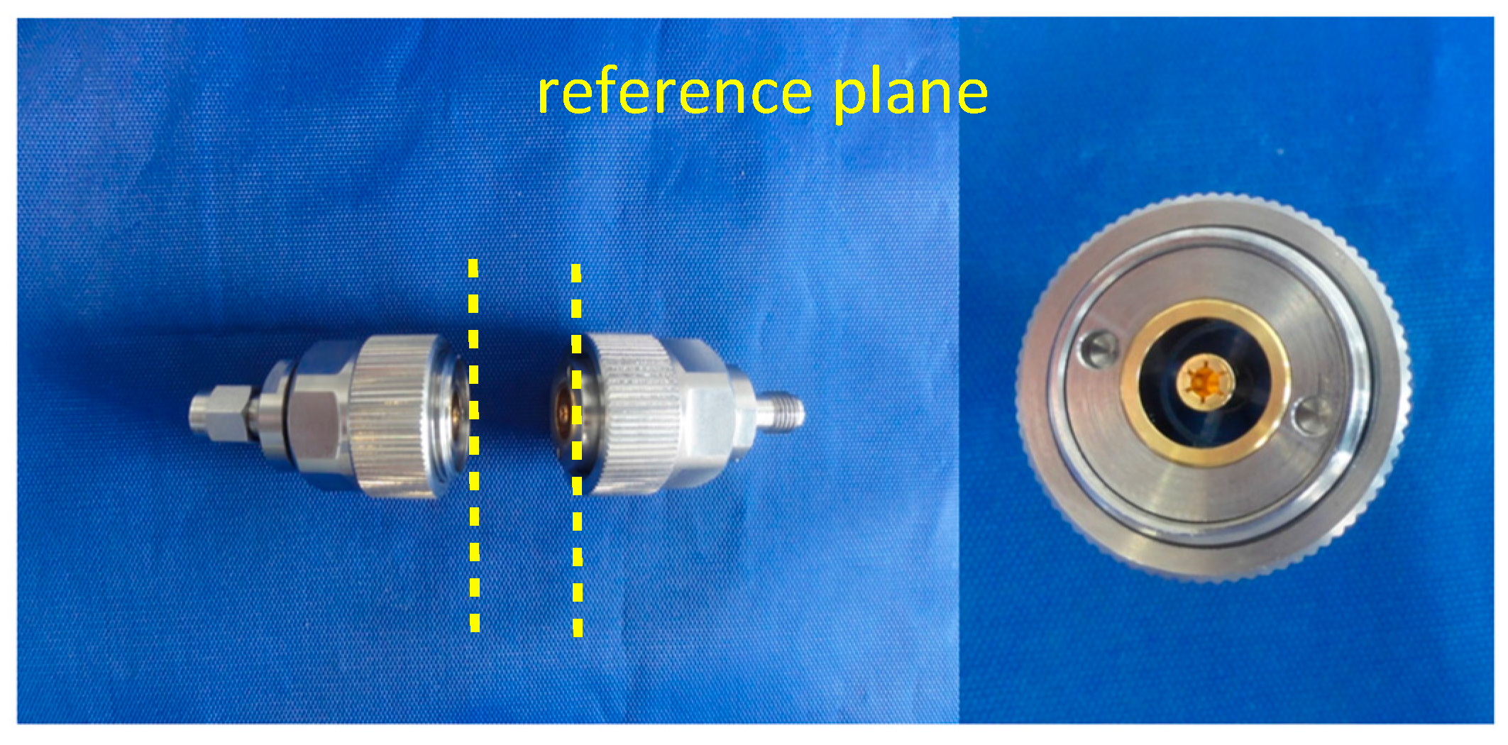
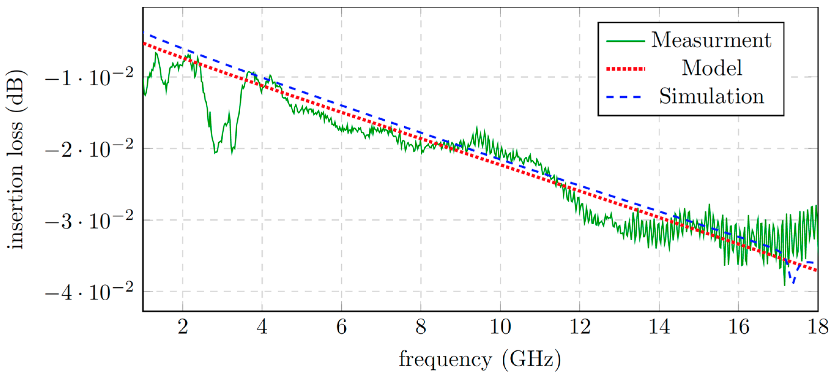
To combine the benefits of measuring the ACP directly between VNA calibration reference planes and the accuracy of coaxial calibration, a less obvious method can be employed: To this end, the ACP specimen is inserted between the faces of two sexless coaxial connectors (e.g., APC-7 series), which before were connected to their related coaxial calibration standards shown in Figure 5. Thus, the specimen is measured directly between these coaxial reference planes with the signal path consisting only of the ACP, its length being the thickness of the specimen. A typical measurement result is shown in Figure 15 of Section 5, the insertion loss of an ACP being 0.04 dB at 18 GHz.
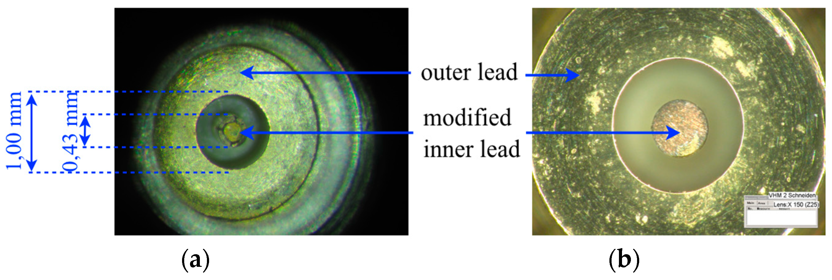
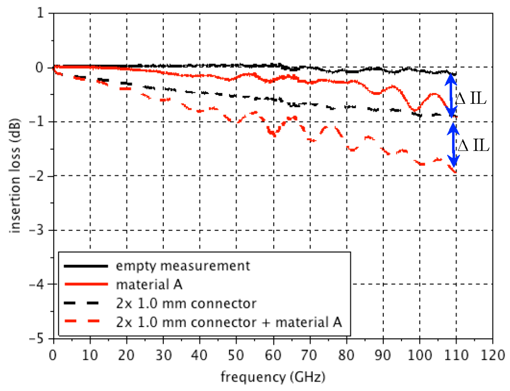
As already described in [6], commercially available sexless coaxial connectors operate only up to 18 GHz. For this reason, pin/socket through standards of a 1.0 mm coaxial calibration kit were used in [6] to achieve high precision results up to 110 GHz with the same measurement principle. Since the pin of the male standard would puncture the ACP, the inner lead together with the pin was cut flush with the outer lead (Figure 6, right). Moreover, the spring fingers of the female standard were filled in order to increase the contact area, thereby ensuring contact for a sufficient number of filaments in the ACP and reducing DC resistance (Figure 6a). Thus, a pair of sexless 1.0 mm connectors is established. Prior to actual measurement, the VNA is calibrated using unmodified pin/socket through standards. After calibration, the unmodified through standards are replaced by the modified sexless pair. This procedure is valid, because the modified connectors are made from calibration standards and therefore are geometrically and electrically identical. Figure 7 shows insertion loss responses measured with such assemblies.
Insertion loss of the modified without ACP inserted (solid black line) fluctuates around 0 dB due to the fact that the reference planes and properties of the modified pair are closely identical to the unmodified through standards. Consequently, the response with ACP inserted (continuous red line) represents the insertion loss solely of the ACP, which is about 1 dB at 110 GHz. For verification purposes, calibration was also performed to the reference planes on the remote interfaces of the two through standards. Thus, the black dashed line shows the insertion loss of the pair of through standards. By inserting an ACP between the standards, this insertion loss is increased by the additional loss of the specimen. Hence, the difference of the red dashed line and the black dashed line again is the insertion loss of the ACP, with a value of about 1 dB, which is consistent to the previous result [6].
Using the same approach, 2.4 mm connectors were also modified in a similar way in order to determine the insertion loss of different ACP materials up to 40 GHz. Only with this type of connector was it possible to measure materials with lower filament density due to the larger area of the inner connector. As displayed in Figure 8, the ACP specimens reveal tremendous performance differences in terms of insertion loss. Moreover, there was a large number of ACPs, whose frequency range is considerably restricted. The related results are not shown here.

4. Extracting Apparent Material Parameters from Measured Data

In order not to characterize the ACP just by the impedance profile or insertion loss of an individual sample, material parameters for use with 3D filed solvers were extracted. As ACPs are composite materials of dielectric matrix and conductive filaments, such figures are not actually physical but “apparent” parameters [7]. These apparent material parameters were obtained according to the methodology described in Section 3.2, using an assembly of two sexless APC7-type connectors where the elastomer is inserted in between. Figure 9 shows a longitudinal cross section through the assembly and its geometrical dimensions, where t describes the thickness of the material under test (MUT).
As per TOSM (through, between all ports, open, short, match at each port) calibration, the reference planes are thus set to the outer surfaces of the ACP specimen, and the assembly can be described by the S-Parameter cascade model in Figure 10.
The transmission line properties γx and ZL,x can be extracted from the measured S-parameters according to
Z L , x = Z 0 ( 1 + S 11 ) 2 S 21 2 ( 1 S 11 ) 2 S 21 2
γ x = 1 l ln ( S 21 1 r S 11 )
where l is the length of the transmission line, and r is the reflection coefficient at the step from the reference impedance (50 Ω) to the line impedance ZL,x.
Due to the pressure that is imposed on the polymer by the inner and outer leads of the APC7-connectors, the polymer itself turns into a short section of a coaxial transmission line. Thus, for the following analysis, the electric and magnetic field distributions may be assumed to be very similar to those of an actual coaxial transmission line:
  • The longitudinal current in the two leads is associated with a transversal magnetic field in an angular direction.
  • The voltage between the leads is related to a transversal radial electric field.
  • The longitudinal current leads to ohmic losses inside regions of finite conductivity.
  • Dielectric losses occur because of the material’s dielectric loss tangent.
Since the metal particles inside the elastomer’s regions not exposed to pressure will influence the fields in a slightly different way than usual homogeneous dielectric material, the following additional field effects have to be involved:
  • The radial electric field will cause a transversal current density J = σE inside the conducting particles, which in turn is related to ohmic losses.
  • The angular magnetic fields will induce current densities inside the metal particles that are also related to ohmic losses.
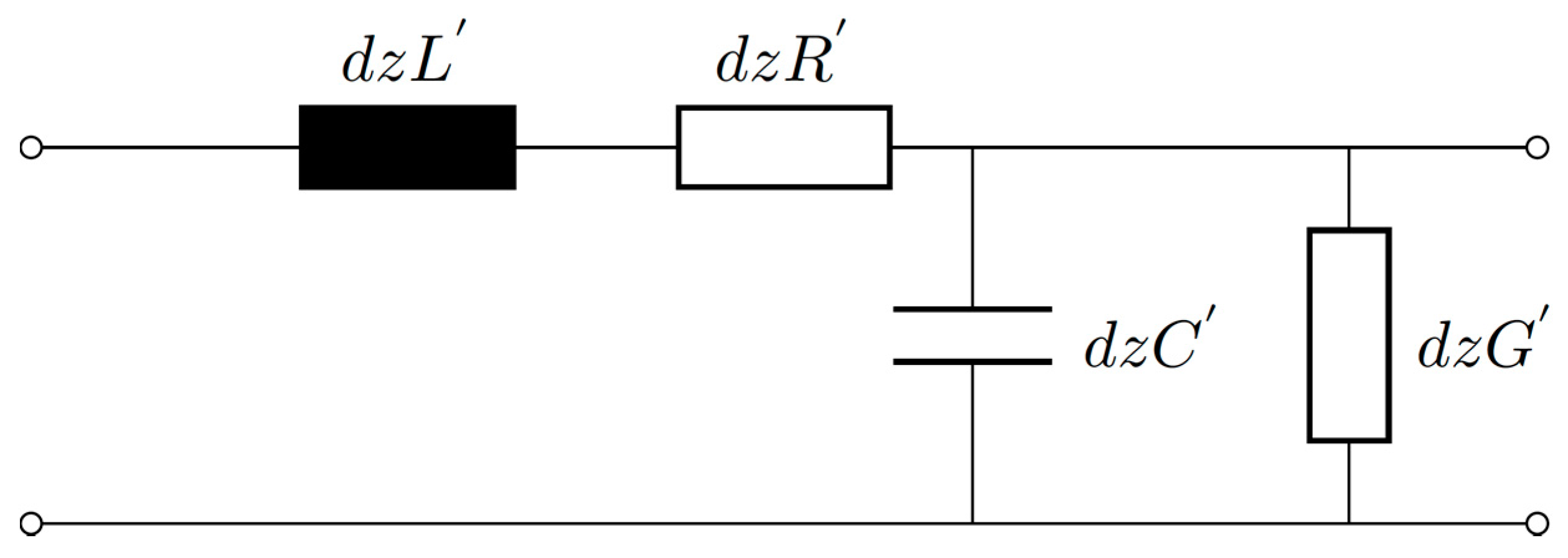
Since the volume of metal particles inside the examined material occupies only a small part of the total volume, the mentioned effects will have little impact on the extracted parameters compared to other uncertainties along the measurement. Following a perturbation approach, the fields will be assumed not to change dramatically due to the additional effects. Hence, the coaxial waveguide formed by the elastomer may also be described by the transmission line model, where a section of infinitesimally small length dz is modeled by the equivalent circuit network shown in Figure 11.
The propagation coefficient γ and characteristic impedance ZL of this line are
γ = ( R + j ω L ) ( G + j ω C )
Z L = R + j ω L G + j ω C
As the four per-unit-length parameters are not sufficient to accurately describe the six effects listed above, it becomes obvious that the extracted values of material properties must be understood as apparent parameters, combining several effects into one. However, the deviation from the pure material properties is considered to stay within an acceptable margin and the final application of the extracted parameters in 3D field simulation software is still justified. As described in [8] from Equations (3) and (4), we can obtain the per-unit-length parameters of the transmission line as follows:
R = { γ x Z x }
L = { γ x Z x } / ω
G = { γ x / Z x }
C = { γ x / Z x } / ω
Since G′ = jωC′ tanδapp, the loss tangent tanδapp can be directly extracted from
tan δ a p p = { γ x / Z x } { γ x / Z x }
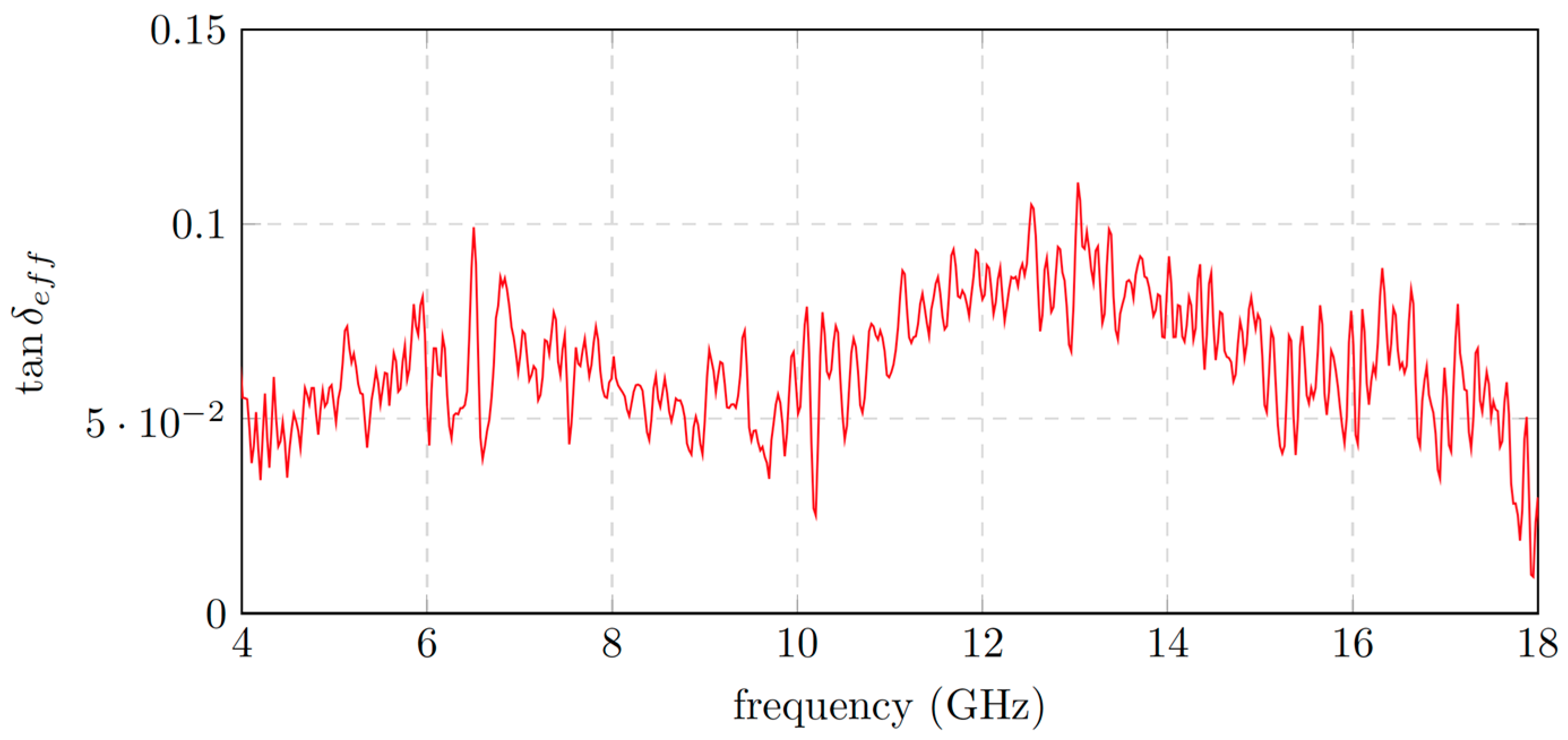
Figure 12 shows the measured response of the extracted apparent tanδ of a 0.2 mm ACP with a thickness of t = 60 µm. From this response, the root-mean-square (RMS) value is taken to obtain a constant material parameter.
By comparing the measured values to the theoretical formulations describing the per-unit-length parameters in coaxial transmission lines [9] and taking into account the effect of inner inductance [10],
L i = R ω
L = L e + L i
L e = μ 2 π ln ( D d )
C = 2 π ε ln ( D / d )
G = ω C tan δ
R = 1 σ ( 1 A o + 1 A i )
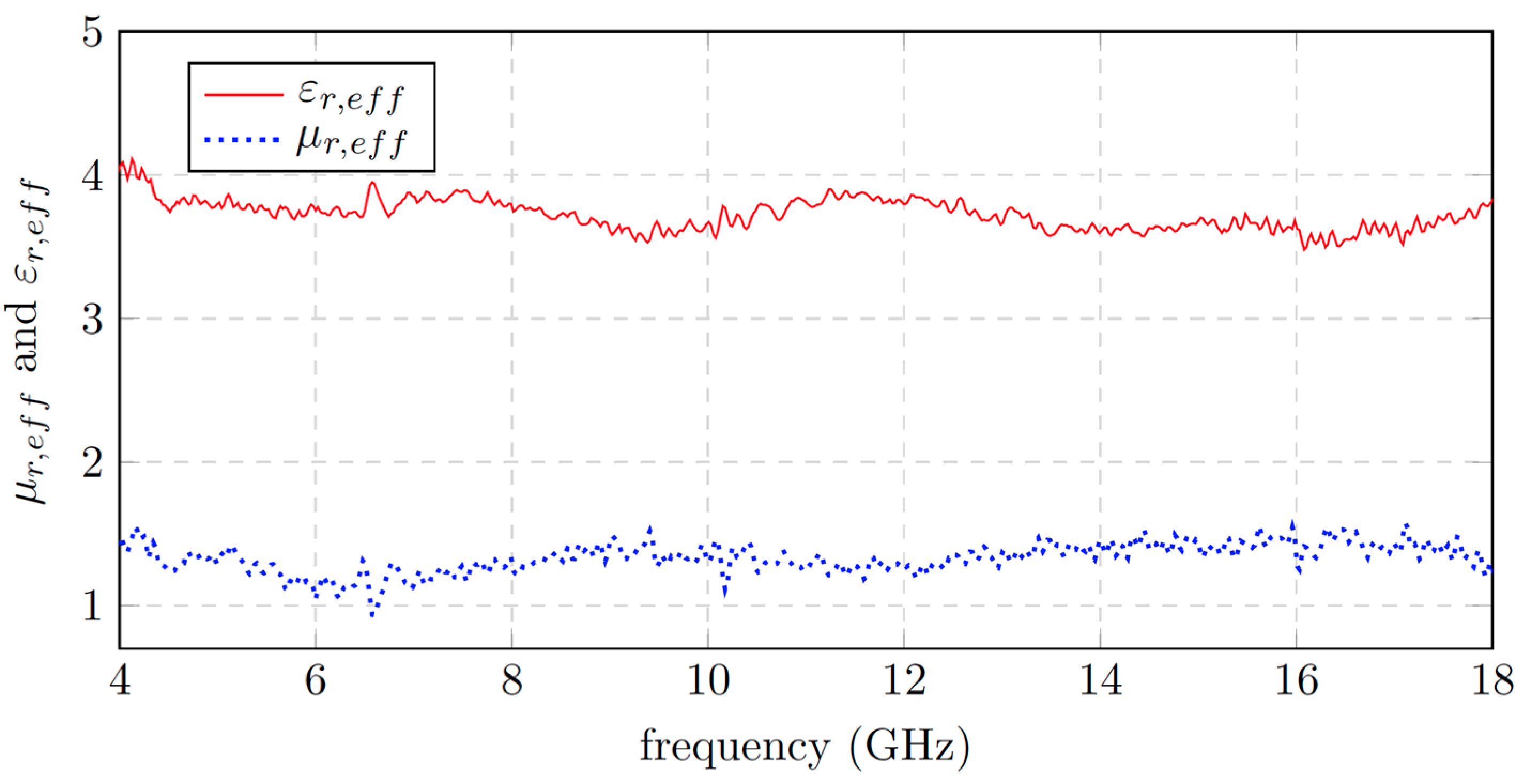
one can solve these equations for µr and εr, which actually yields the desired apparent figures. Measured data are visualized in Figure 13 for the elastomer sample described above. The relatively constant response of both parameters justifies averaging by taking the RMS values.
Evaluating R′ according to Equations (5) and (15) reveals a very low conductivity in the order of 101 S/m to 103 S/m. On the one hand, it is sufficiently high to neglect displacement currents; on the other hand, the finite lead thickness must be taken into account when calculating the skin-depth for the current densities leading to equivalent skin-depths δ′. An analytical approximation based on the plane skin effect assumes the current density’s magnitude to decline in an exponential manner inside conducting matter. At the same time, the total current must stay the same among the whole lead surface over different frequencies. Consequently, the equivalent skin-depth can be formulated as
δ = δ 0 ( 1 e a / δ 0 )
where δ0 is the plane skin depth and a represents the lead thickness. Using δ′ and the assembly’s geometry data, the formulation for the per-unit-length resistance R′ is found according to Equation (15) with
A o = π ( R + δ 0 ) 2 π R 2
A i = π r 2 π ( r δ i ) 2
where δ0′ and δi′ are the equivalent skin depths, and R and r are the radii of the outer and inner lead, respectively.
In order to find the correct conductivity, all other apparent material parameters are first estimated as described. With these, the value for the apparent conductivity is found by minimizing the deviation of the calculated from measured response.

5. Verification

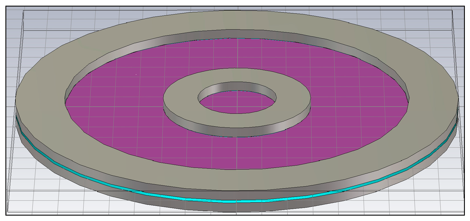
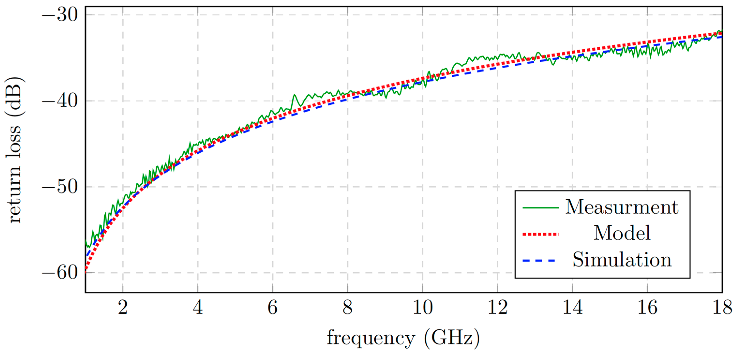
For the examined ACP, the described procedure delivers the following material parameters εr,app = 3.72, µr,app = 1.33, tanδapp = 0.066, and σl,app = 548 S/m. These parameters allow for the simulation of the assembly with the 3D FEM field solver Microwave-Studio by CST. A waveguide port was used for excitation of a short section of coaxial wavegeuide in the frequency domain. The ASP was inserted between the two faces of the guides, as shown in Figure 14. In particular, the compressed areas between the leads were modeled as lossy metal with the aforementioned parameter σl,app = 548 S/m, and the non-compressed areas were modeled as dielctric. Figure 15 and Figure 16 show the comparison between the measured, modeled, and simulated assemblies in very good agreement.

6. Effects of ACPs on Crosstalk

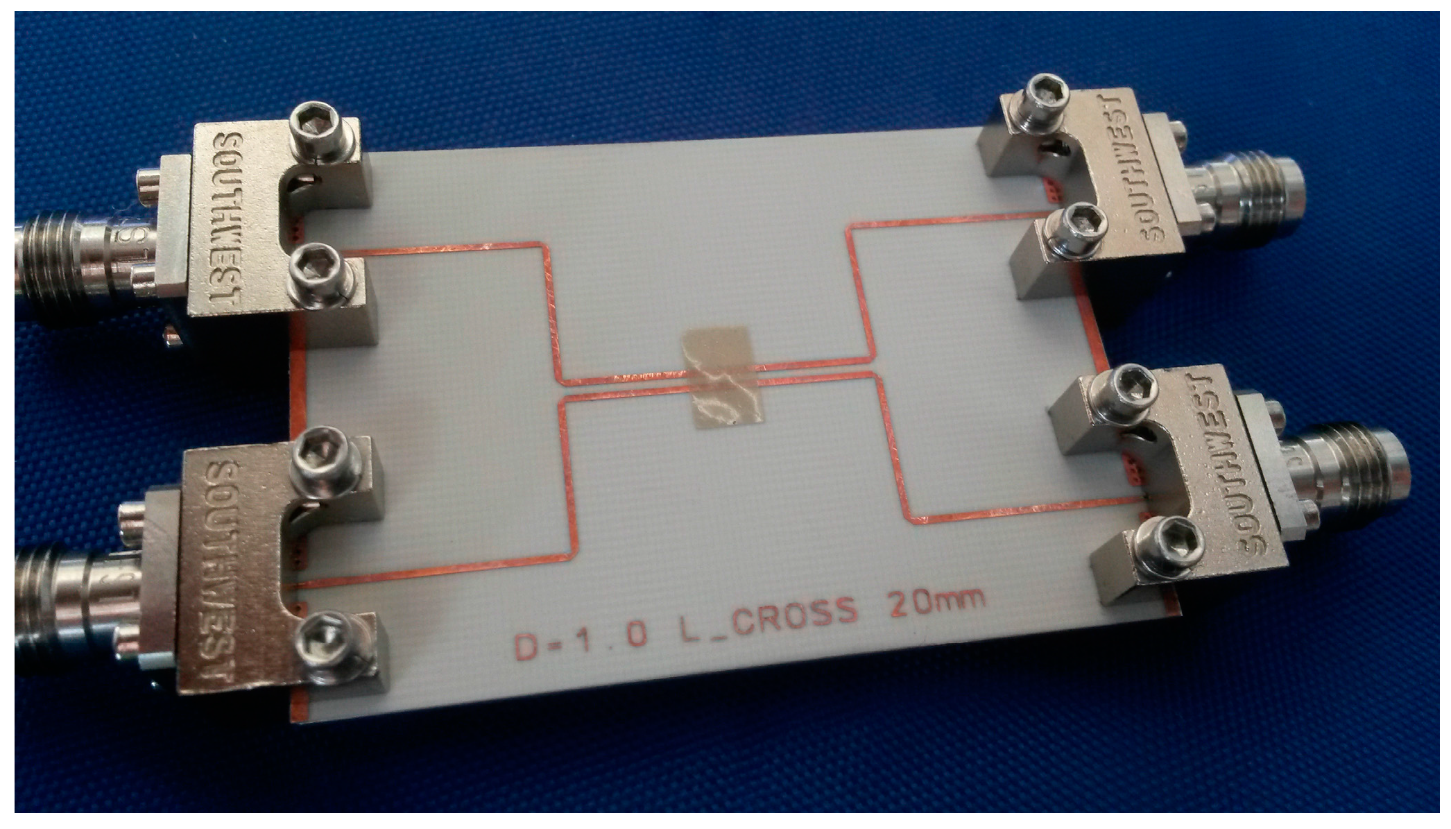
Due to the the vertical arrangement of the embedded contact filaments in an ACP and their low mutual distance, it would be justified to assume a strong capacitive coupling between adjacent signal paths in a horizontal direction, especially as there are always floating filaments in between the regions with filaments establishing contact. As a consequence, these conducting polymers would lead to unwanted additional crosstalk effects when inserting them e.g., between a small pitch ball grid array (BGA) package of an integrated circuit and the related PCB contact pads on a test fixture. To investigate such parasitic capacitive coupling, several types of measurement assemblies were designed to quantify both far end and near end crosstalk effects (FEXT, NEXT) of ACP inserted between transmission lines resp. contact pads. The first type of assembly is displayed in Figure 17 and consists of two coupled microstrip lines connected to end launch connectors. Different coupling factors were accomplished by implementing the coupled line structures with different gap widths. The generator output of a vector network analyzer (VNA) is fed into one of the end launch connectors, while the output on all other connectors is measured by the VNA receivers. Thus, besides insertion loss of the operated transmission line (aggressor), FEXT and NEXT to the other line (victim) are observed. Crosstalk is going to happen almost entirely between those sections of the microstrip lines that run closely parallel to each other, as the feeding sections depart perpendicularly to the coupled sections. Feed lines, bends, and coupled lines are all impedance-matched. The objective is to acquire information on how a conducting polymer placed above the coupled lines alters the amount of the two crosstalk types FEXT and NEXT.
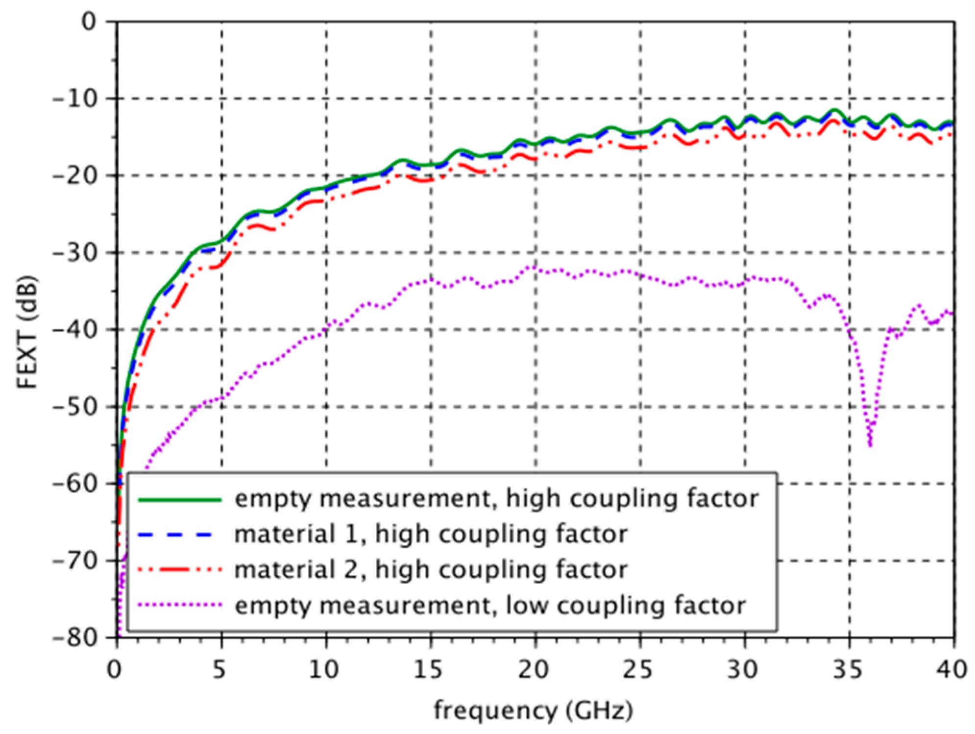
Figure 18 and Figure 19 show FEXT and NEXT, respectively, measured on strongly coupled transmission lines without an ACP specimen (solid green) and with two different ACP specimens (dashed blue and dash-dotted red, respectively) in comparison to weakly coupled lines without an ACP specimen (dotted violet).
In contrast to the intuitive assumption, conducting polymer placed above the strongly coupled coupled transmission lines slightly increases only NEXT for frequencies up to 10 GHz, whereas it is reduced for higher frequencies, as is FEXT for the entire frequency range. One possible explanation is that the field concentrates mostly below the microstrip lines in the dielectric and hence the space between and above the lines, where the ACP is located, is not sufficiently penetrated by the EM field. Therefore, the second type of assemblies (Figure 20) consists of two identical PCBs with four contact pads, as used for BGA packages, closely parallel to the edges of the PCBs. The inner two of these pads are connected to the ends of the signal traces of two microstrip lines, while the outer two pads establish contact with the ground planes on the back sides of the PCBs, thus forming a ground–signal–signal–ground (GSSG) contact pattern. All microstrip lines are connected to end launch connectors at their other ends. As described in Section 3.1, in this “planar transmission line contact methodology”, one PCB is placed upside down onto the other such that the open ends of the transmission lines are slightly overlapping. Microstrip line geometry was modified in the overlap region in order to maintain impedance matching when both PCBs are brought to contact. Measurements were taken without and with an ACP specimen inserted between the overlap region. As a result, the inserted specimen is completely penetrated by the EM field and could lead to considerable crosstalk effects.
Figure 21 and Figure 22 show FEXT and NEXT measured on the same contact pad grid with a pitch of 0.8 mm without an ACP specimen (“empty”, solid green) and with three different ACP specimens (dashed blue, dash-dotted red, and dotted violet). In comparison to the empty measurement, all investigated materials cause no appreciable effects, neither on FEXT nor on NEXT. However, the coupling between the feed lines could be large compared to the crosstalk effects at the overlap region, thus concealing crosstalk in the overlap region. Therefore, further efforts were undertaken to determine the effects of conducting polymers between BGA pads.
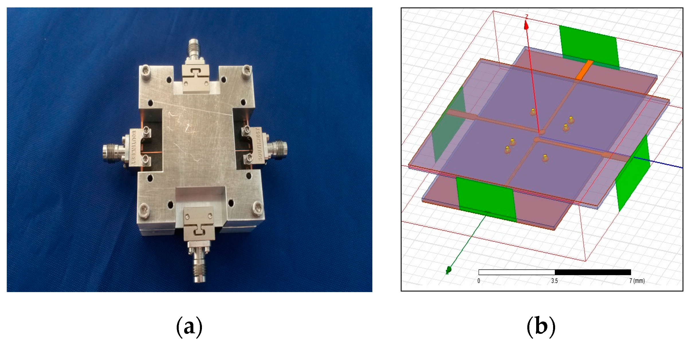
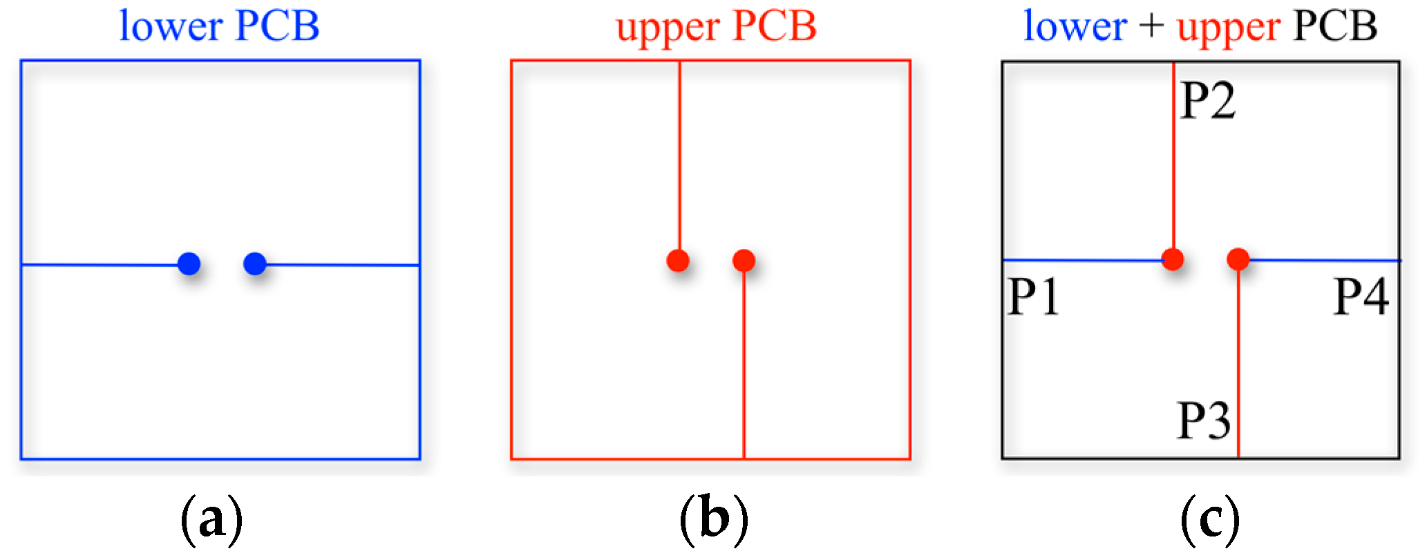
To create a situation closely comparable to future application in test fixtures and to exclude the coupling influence of adjacent feed lines, the concept of a third assembly is displayed in Figure 23. This planar BGA contact pad set-up comprises two different PCBs, whose common interface exclusively consists of the BGA pads of the upper and lower PCBs (Figure 24). The feed lines are arranged such that no appreciable additional crosstalk can occur, i.e., perpendicular to each other. Worth mentioning is the fact that FEXT and NEXT become identical with this measurement assembly, as crosstalk is going to occur in a point-shaped region only. Thus, a signal input to Port 1 creates the same crosstalk on Port 3 and Port 4. In either case, the measurement result is the crosstalk between two pairs of adjacent BGA pads, connected by an ACP.
Again, measurements were taken without and with ACP specimens inserted between the BGA contact pads.
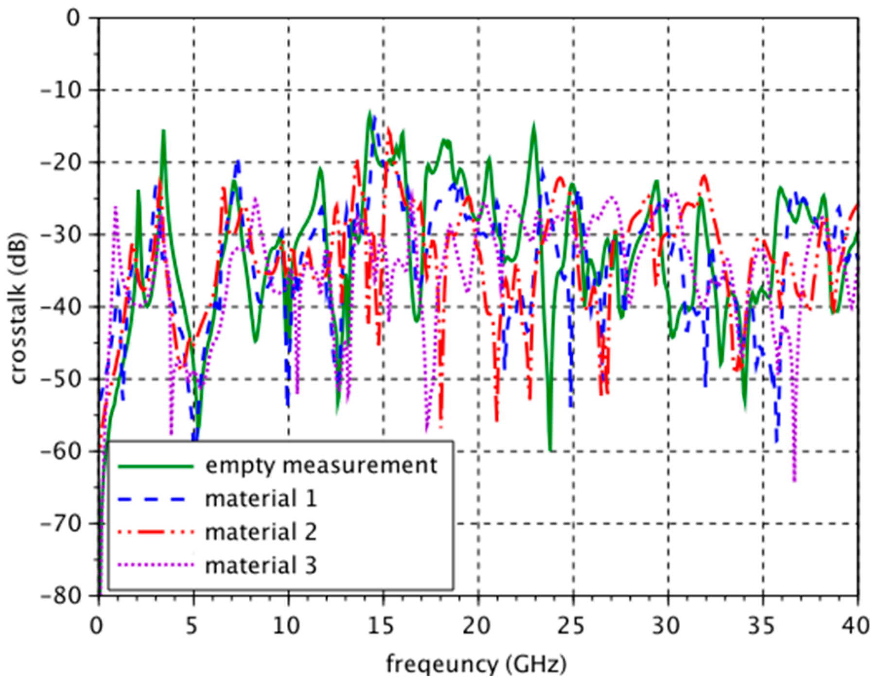
The red continuous line of Figure 25 represents the empty measurement. Based on a comparison to that, the insertion of all types of investigated anisotropic conducting polymer does not result in any additional appreciable crosstalk. Contrary to the initial, intuitive assumption mentioned at the beginning of this section, the investigated materials do not increase crosstalk effects between lines or BGA pads. Therefore, the application of thin anisotropic conducting polymers as temporary microwave interconnects in test fixtures is not limited because of additional crosstalk. This observation is also in accordance with the relatively high apparent loss tangent of the ACP inferred by the considerations in Section 4, which causes sufficient attenuation in the transversal direction.

7. Reliability

Besides the electrical performance of ACPs—which was demonstrated to be very promising in the previous sections—high reliability is a requirement for application in test fixtures. For high reliability in application, correct mechanical handling, with an emphasis on the influence of contact force, is crucial.
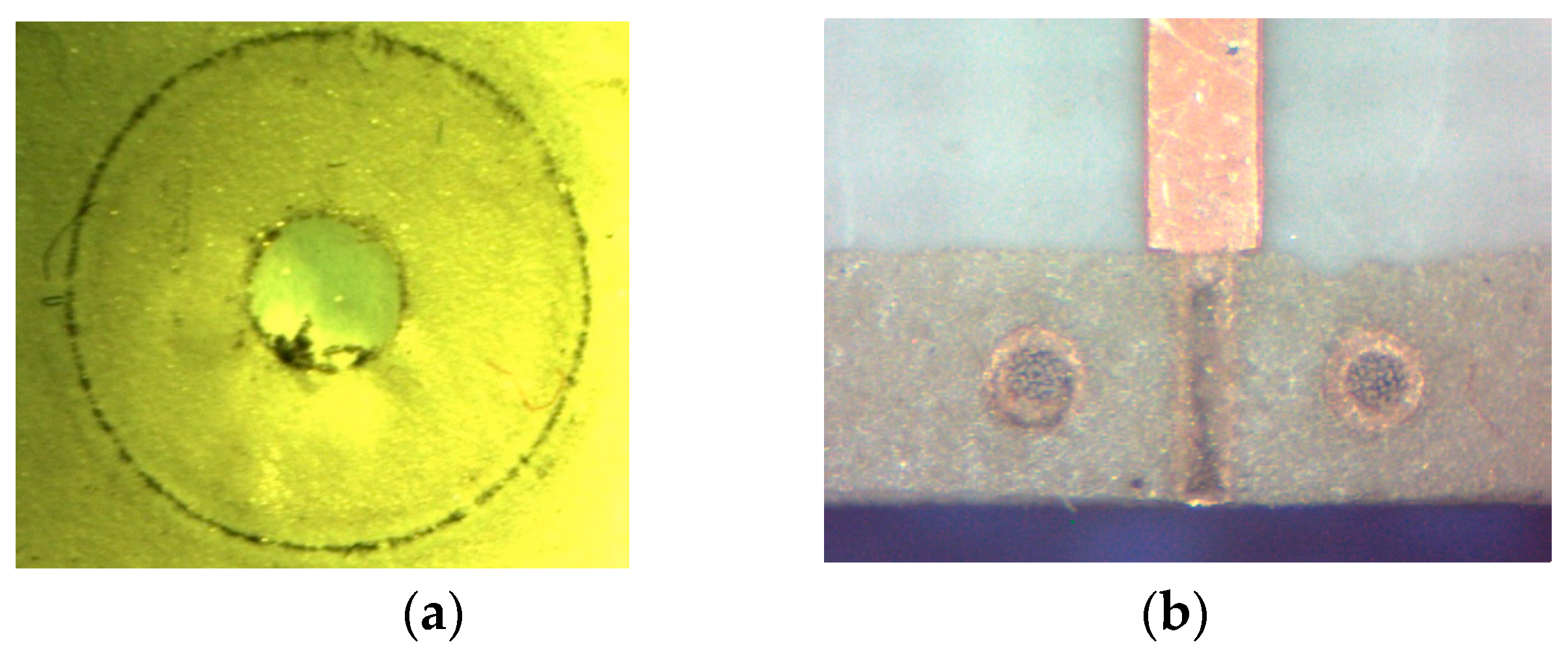
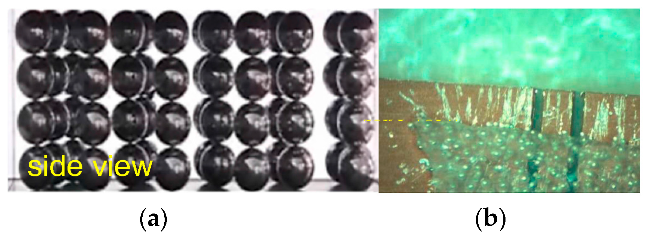
One cause of defect is illustrated in Figure 26. On the left, the side view of a virgin ACP with pins as conducting elements is shown, whereas on the right, the same specimen is depicted after a single contact cycle at increased contact force, which led to irreversible damage. In contrast, conducting polymers with spheres turned out to be much more durable under increased contact forces. However, in these materials, the filaments tend to agglomerate under increased contact forces after high cycle counts. This phenomenon is depicted on the left side of Figure 27. The outer black circle originates from agglomerated spheres after 105 contact cycles between the outer conductors of sexless coaxial connectors. The part of the inner conductor is even ruptured for the same reason. However, these agglomerations did not lead to any influence with regard to the electrical parameters. The right side of Figure 27, for example, shows the microstrip-to-microstrip assembly from Section 3 revealing spheres agglomerated after 300 contact cycles under a contact force 10 times higher than suggested by the vendor. Despite the obvious structural deterioration, the signal propagation parameters did not exhibit any deviation from those of the un-deteriorated conducting polymer. Generally, the measured insertion loss of this material turned out to be quite insensitive to different contact forces. To avoid such agglomerations, it is necessary to calculate the contact force from the recommended force per area figure, multiplying by the actual contact footprint area only instead of the entire ACP area. Another challenge consists in printed circuit boards that are largely uneven. Intending to ensure a reliable contact, PCBs are often pressed too hard onto the test fixture, causing deterioration discussed above. It is therefore important to define a limit for the unevenness of printed circuit boards.
8. Application in Test Fixtures

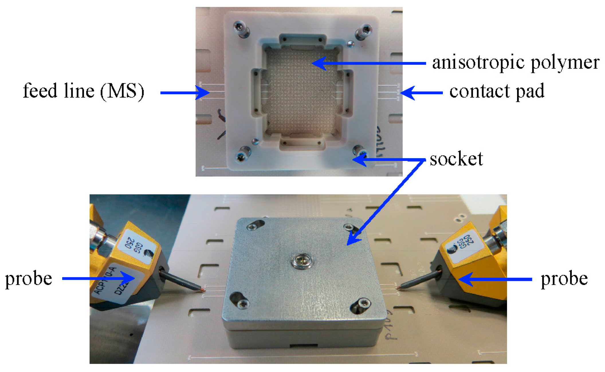
As already described in [6], a simple method for temporarily contacting ICs for microwave applications is to use a PCB with the IC footprint, to connect both by interposing an ACP and to fix all by an appropriate mechanical assembly. Figure 28 shows the transition from a PCB to the device under test (DUT) with a BGA grid via an ACP. Using a chip consisting only of a through line in an inner layer as the DUT, the performance of the ACP in test fixture application can be comprehensively evaluated. The signal path is as follows: coaxial jack—probe—pad—microstrip line (feed line)—BGA—ACP—dummy chip with via—ACP—BGA—microstrip line—pad—probe—coaxial jack [6].
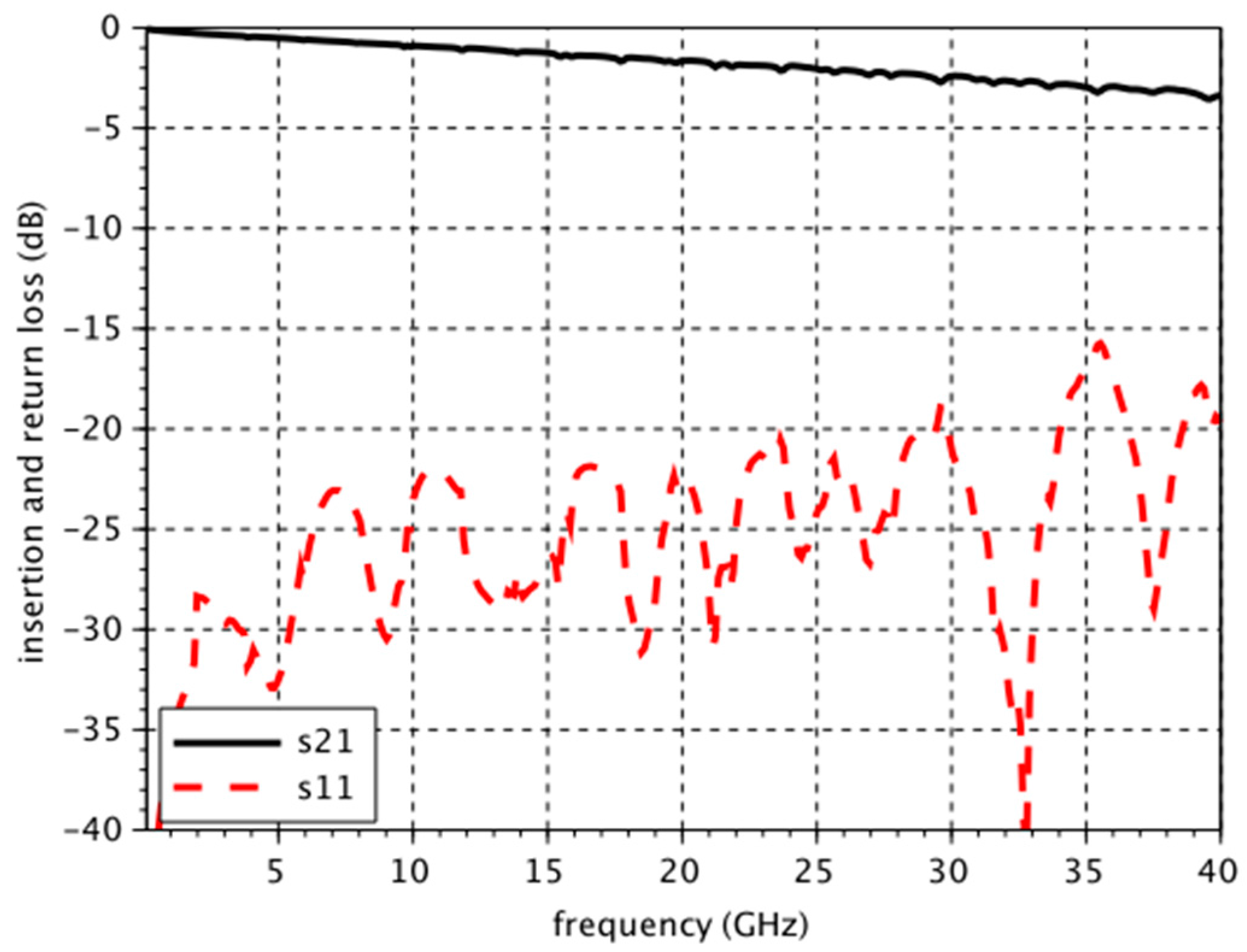
Despite the fact that Figure 29 represents an end-to-end measurement, where the reference planes were located at the coaxial part of the GSG-probes and a certain mismatch was present at the transition to the DUT, very promising measurement results were achieved. Up to 40 GHz, the return loss was below −20 dB except for a small peak at 35 GHz, and insertion loss steadily climbed to only about 3.5 dB at 40 GHz.

9. Conclusions

In this paper, newly developed measurements methodologies for quantifying the electrical performance of ACPs are presented, and their applications are described. The measured ACPs showed tremendous differences in terms of insertion loss. High-end ACPs suggest that test fixtures up to 110 GHz are feasible, as already postulated in the headline. In addition, the developed measurement methods are even capable of determining apparent material parameters of these very thin composite materials, which enables straightforward modeling and use in field solvers, which has been verified in an exemplary case. Despite initial intuitive assumptions, specific measurements show that ACPs do not cause additional crosstalk. Reliability tests showed that, as long as ACPs are treated carefully regarding contact force, microwave applications are feasible, especially when temporary contacting is needed, as the signal integrity results here suggest. These detailed results were confirmed by the promising overall performance of a prototype test fixture.

Acknowledgments

The authors would especially like to thank Christian Riedel at Rohde & Schwarz, Teisnach, Germany, for valuable discussion and precise measurements as well as for the sophisticated modification of the 1.0 mm calibration standard. The reported results were obtained in the course of the project INTERAPID (AZ-1057-12), funded by the BFS (Bavarian Research Foundation).

Author Contributions

All authors contributed to the paper K. Helmreich, G. Gold and M Sippel contributed to the Characterization Methodologies, Effect of ACPs on crosstalk, Application in Test Fixtures and Reliability. K. Lomakin dealed with chapter 4 and 5: Extracting Apparent Material Parameters from Measured Data and Verification.

Conflicts of Interest

The authors declare no conflict of interest.

References

  1. Faller, H.L. RF Wireless and High Speed Digital Test Issues and Your Contactor Supplier. Johnstech International Corporation. Available online: http://www.johnstech.com/tech-support/technical-papers.php (accessed on 12 December 2017).
  2. Tunaboylu, B. Electrical Characterization of Test SocketsWith Novel Contactors. IEEE Trans. Device Mater. Reliab. 2014, 14, 580–582. [Google Scholar] [CrossRef]
  3. Weiss, R.; McMorrow, S. Feasability of 40 to 50 Gbps NRZ Interconnect Design for Terabit Backplanes. In Proceedings of the 19th DesignCon East Week, Worcester, MA, USA, 19–21 September 2005. [Google Scholar]
  4. Jin, S.; Sherwood, R.C.; Mottine, J.J.; Tiefel, T.H.; Opila, R.L. New, Z-direction anisotropically conductive composites. J. Appl. Phys. 1988, 64, 6008. [Google Scholar] [CrossRef]
  5. Weiss, R.; Barnum, D. High Speed Connections: It Takes BallWires® to Connect to 40 GHz and Beyond. Available online: http://test.paricon-tech.com/Documents/Documents-folder:PARIPOSER:OVERVIEW/ (accessed on 12 December 2017).
  6. Sippel, M.; Gold, G.; Helmreich, K. Signal Propagation Properties of Anisotropic Conducting Polymers up to 110 GHz and their Applicability in Test Fixtures. In Proceedings of the 20th IEE Workshop on Signal and Power Integrity, Turin, Italy, 8–11 May 2016. [Google Scholar]
  7. Gold, G.; Helmreich, K. Measuring Design-DK and True Permittivity of PCB Materials up to 20 GHz. In Proceedings of the 9th German Microwave Conference (GeMiC2015), Nuremberg, Germany, 16–18 March 2015; pp. 154–157. [Google Scholar]
  8. Eisenstadt, W.R.; Eo, Y. S-parameter-based IC interconnect transmission line characterization. IEEE Trans. Compon. Hybrids Manuf. Technol. 1992, 15, 483–490. [Google Scholar] [CrossRef]
  9. Pozar, D. Microwave Engineering; Wiley: Hoboken, NJ, USA, 2012. [Google Scholar]
  10. Heinrich, W. Quasi-TEM description of MMIC coplanar lines including conductor-loss effects. Trans. Microw. Theory Tech. 1993, 41, 45–52. [Google Scholar] [CrossRef]
Figure 1. Anisotropic conducting polymer (ACP) with BallWire® technology (Adapted with permission from [5], Paricon Technologies Inc., 2017) (a) silver-plated nickel spheres stapled to chains (b) penetration of the oxide layer.
Electronics 06 00109 g001
Figure 2. Photograph of an ACP with ZebraStripesTM technology.
Electronics 06 00109 g002
Figure 3. Planar transmission line contacts connected with ACP (Adapted with permission from [6], IEEE, 2017).
Electronics 06 00109 g003
Figure 4. Impedance profiles of planar transmission line contacts (Adapted with permission from [6], IEEE, 2017).
Electronics 06 00109 g004
Figure 5. Sexless coaxial connectors (e.g., APC-7 series) with planes highlighted by dashed yellow lines.
Electronics 06 00109 g005
Figure 6. Modified 1.0 mm calibration kit (through) to measure ACP properties up to 110 GHz, (a) modified 1.0 mm male standard (b) modified 1.0 mm female standard [6].
Electronics 06 00109 g006
Figure 7. Insertion loss of an ACP measured with different reference planes (Reproduced with permission from [6], IEEE, 2017).
Electronics 06 00109 g007
Figure 8. Insertion loss of different ACPs. (Reproduced with permission from [6], IEEE, 2017)
Electronics 06 00109 g008
Figure 9. Longitudinal cross section of the measurement assembly.
Electronics 06 00109 g009
Figure 10. Schematic representation of the assembly.
Electronics 06 00109 g010
Figure 11. Equivalent network of a TEM-Waveguide.
Electronics 06 00109 g011
Figure 12. Extracted apparent tanδ of a 0.2 mm pitch ACP, t = 60 µm.
Electronics 06 00109 g012
Figure 13. Extracted apparent relative permeability and permittivity of a 0.2 mm pitch ACP, t = 60 µm.
Electronics 06 00109 g013
Figure 14. Design of the coaxial waveguide in CST.
Electronics 06 00109 g014
Figure 15. Insertion loss: Measurement vs. Model vs. Simulation.
Electronics 06 00109 g015
Figure 16. Return loss: Measurement vs. Model vs. Simulation.
Electronics 06 00109 g016
Figure 17. Coupled microstrip line assembly with an ACP specimen on top.
Electronics 06 00109 g017
Figure 18. FEXT of coupled microstrip lines without and with two different ACP specimens in comparison to weakly coupled lines without an ACP specimen.
Electronics 06 00109 g018
Figure 19. NEXT of coupled microstrip lines without and with two different ACP specimens in comparison to weakly coupled lines without an ACP specimen.
Electronics 06 00109 g019
Figure 20. (a) Planar transmission line contact assembly with parallel microstrip lines; (b) ACP between the overlap region for complete field penetration.
Electronics 06 00109 g020
Figure 21. FEXT measured with the planar transmission line contact assembly of Figure 19 without an ACP specimen inserted and with three different ACP specimens.
Electronics 06 00109 g021
Figure 22. NEXT measured with planar transmission line contact assembly of Figure 19 without an ACP specimen inserted and with three different ACP specimens.
Electronics 06 00109 g022
Figure 23. (a) Planar BGA contact pad assembly with orthogonal feed lines; (b) ACP between BGA pads in the overlap region.
Electronics 06 00109 g023
Figure 24. Concept of planar BGA contact pad assembly from Figure 23. (a) lower PCB (b) upper PCB (c) lower+upper PCB
Electronics 06 00109 g024
Figure 25. Crosstalk measured with planar BGA contact pad assembly of Figure 23 without an ACP specimen inserted and with three different ACP specimens.
Electronics 06 00109 g025
Figure 26. (a) ACP with embedded pins: virgin state (b) after one contact cycle under increased contact force.
Electronics 06 00109 g026
Figure 27. ACP with embedded spheres. (a) agglomerated after >100 contact cycles between sexless connectors (b) microstrip-to-microstrip transition.
Electronics 06 00109 g027
Figure 28. PCB to chip transition with test socket and ACP as temporary microwave interconnect (Adapted with permission from [6], IEEE, 2017).
Electronics 06 00109 g028
Figure 29. Return and insertion loss in dB measured end to end (Reproduced with permission from [6], IEEE, 2017).
Electronics 06 00109 g029