
Recent Advances in Electronic and Optoelectronic Devices Based on Two-Dimensional Transition Metal Dichalcogenides


Abstract
:1. Introduction
2. Field Effect Transistors
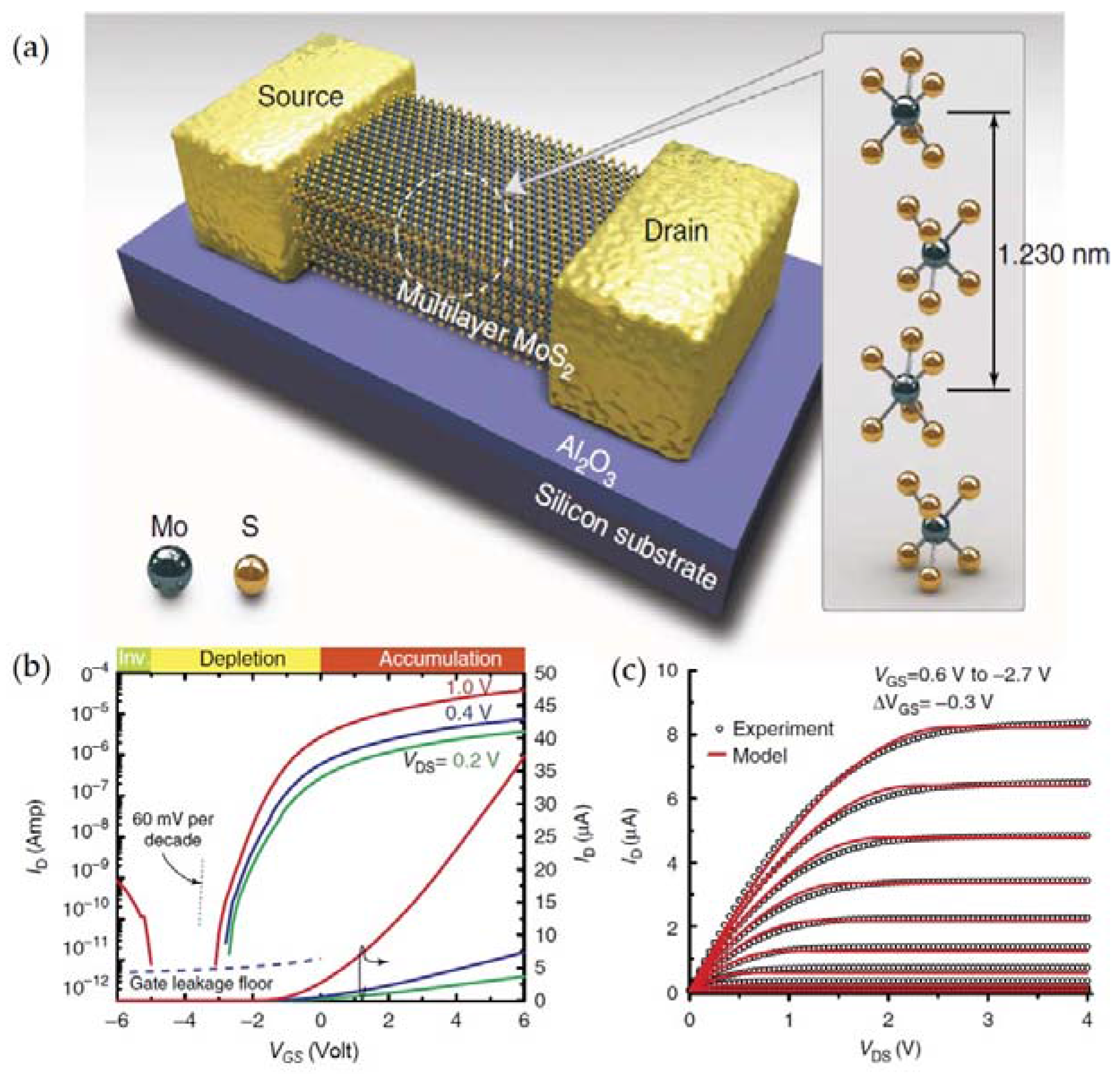
2.1. Transistors with Multilayered TMDCs
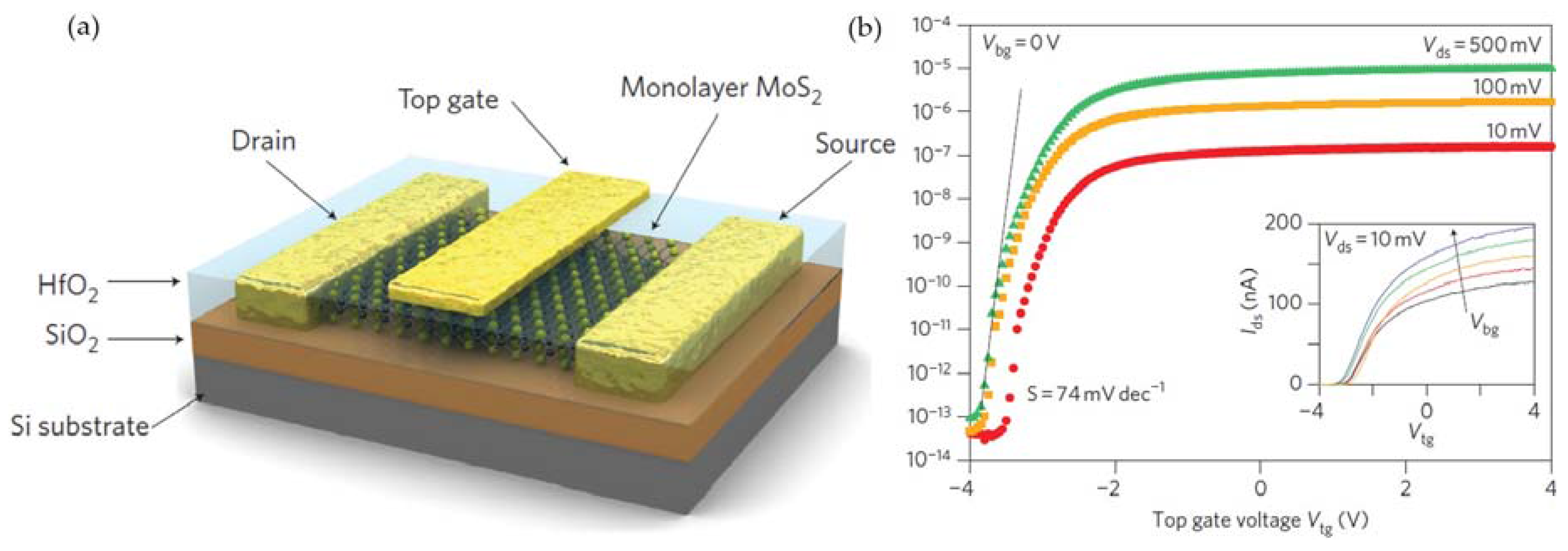
2.2. Transistors with Monolayer TMDCs
2.3. Ambipolar Transistors with TMDCs
2.4. Transistors with Vertical Hetero-Structures
3. Optoelectronic Devices
3.1. Solar Cells
3.2. Light-Emitting Diodes
3.3. Photodetectors
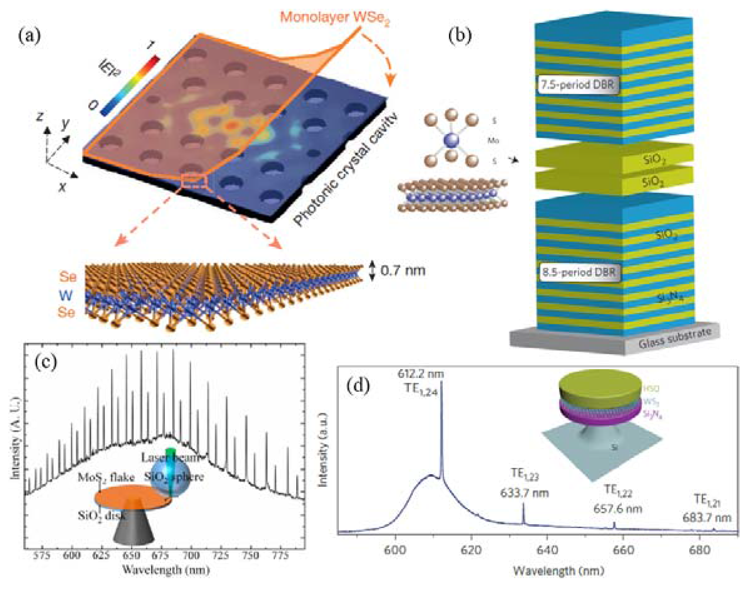
3.4. Lasers
4. Integrated Circuits
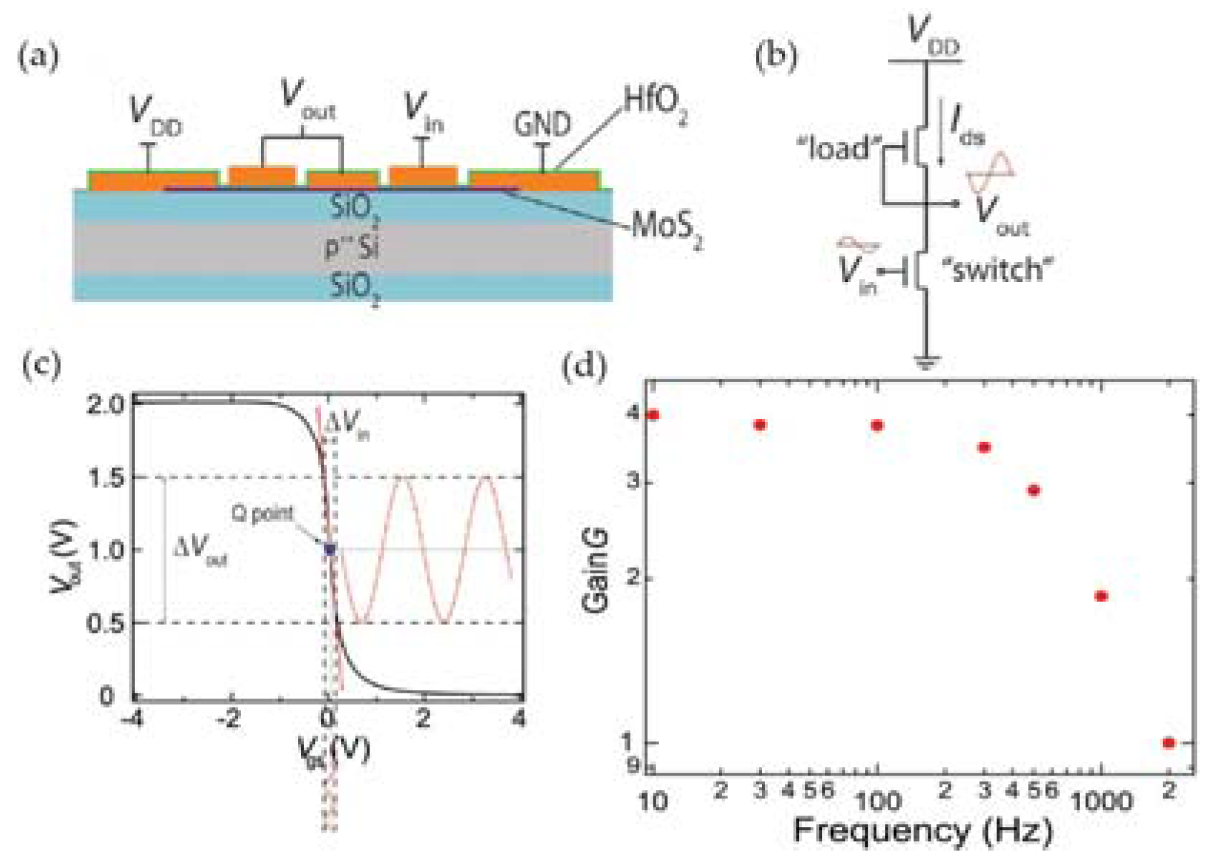
4.1. Amplifiers and Inverters
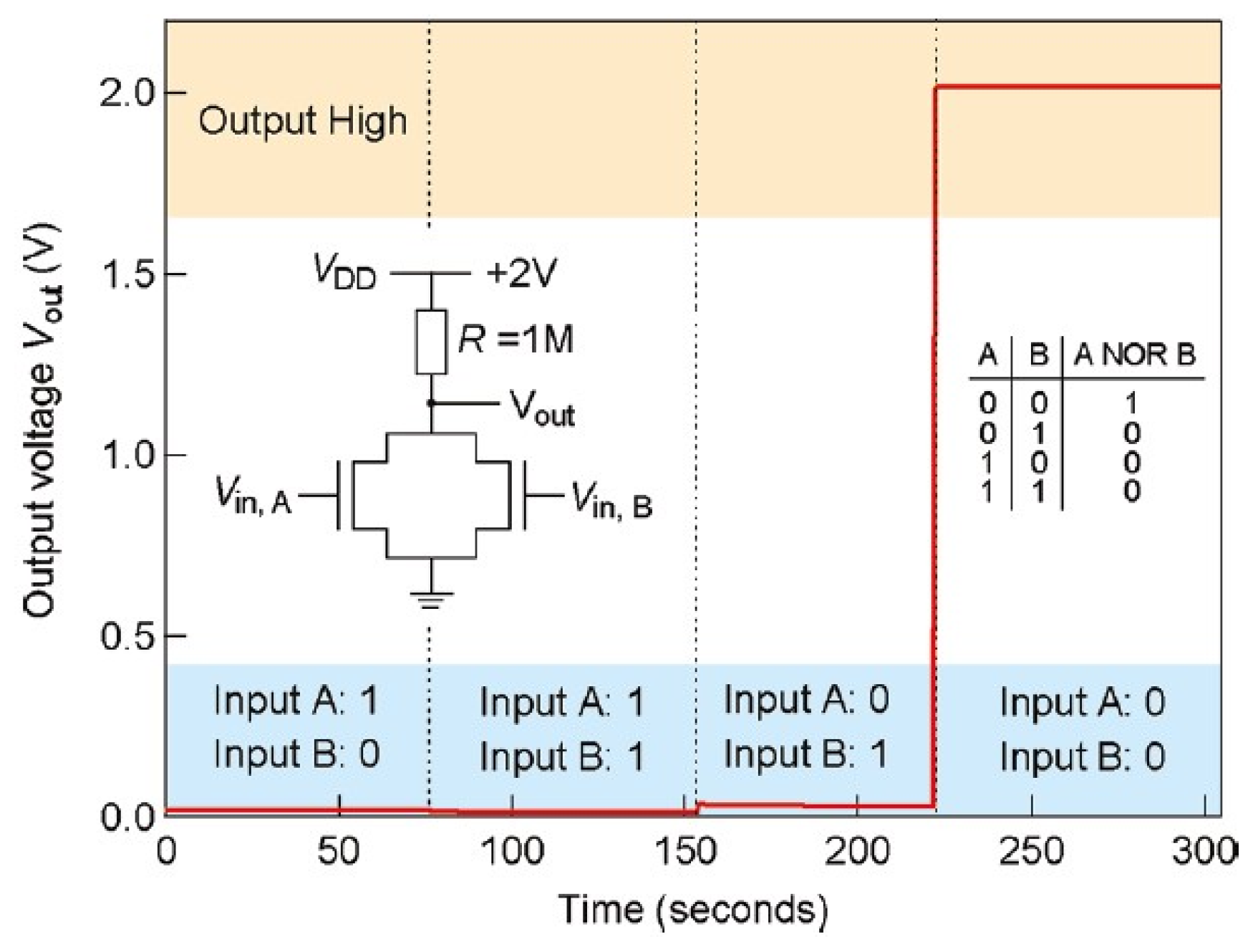
4.2. Logic Circuits
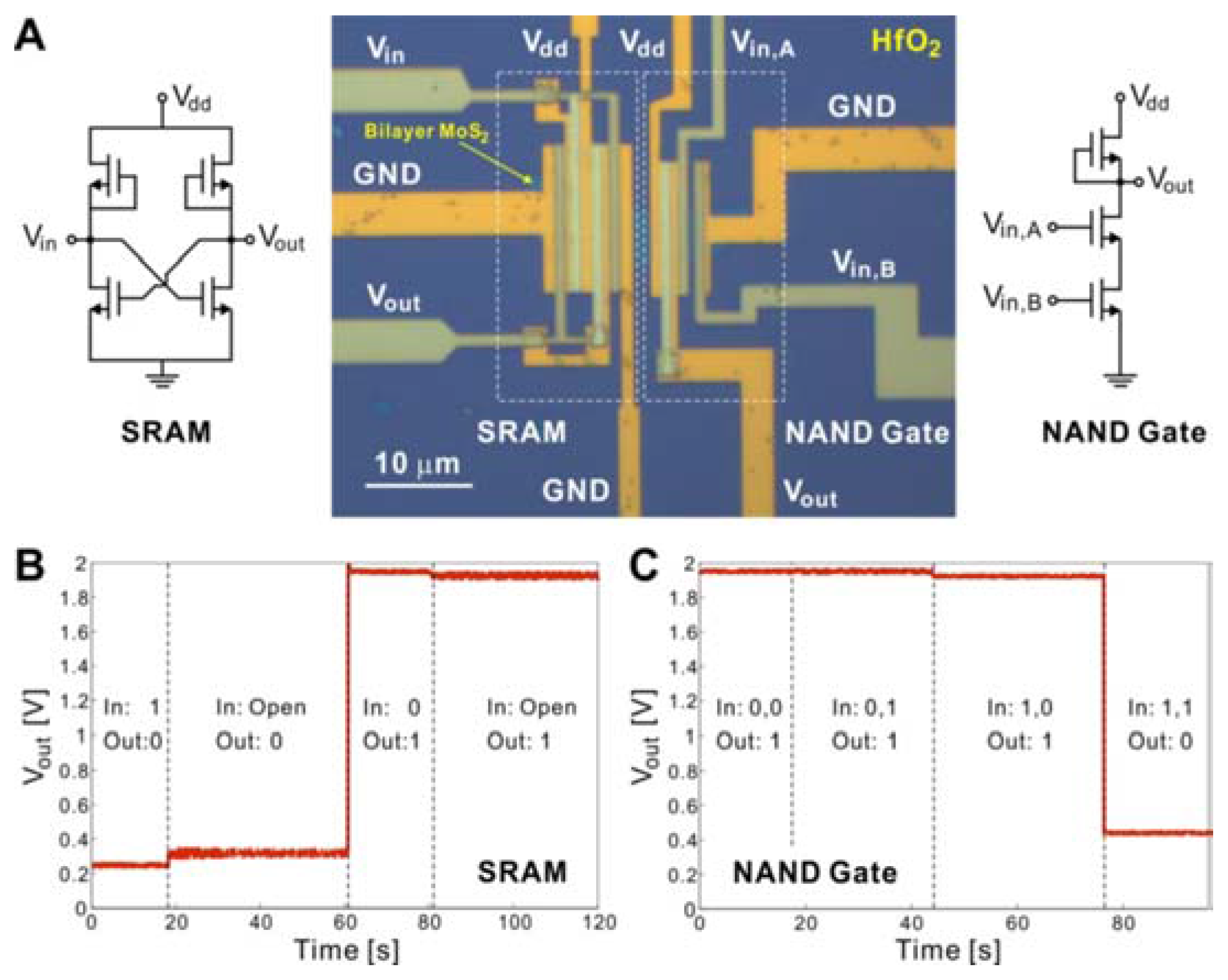
4.3. Memory Devices
5. Summary
Acknowledgments
Author Contributions
Conflicts of Interest
References
- Lundstrom, M. Applied physics. Moore’s law forever? Science 2003, 299, 210–211. [Google Scholar] [CrossRef] [PubMed]
- Theis, T.N.; Solomon, P.M. It’s time to reinvent the transistor! Science 2010, 327, 1600–1601. [Google Scholar] [CrossRef] [PubMed]
- Morton, J.J.; McCamey, D.R.; Eriksson, M.A.; Lyon, S.A. Embracing the quantum limit in silicon computing. Nature 2011, 479, 345–353. [Google Scholar] [CrossRef] [PubMed]
- Ferain, I.; Colinge, C.A.; Colinge, J.P. Multigate transistors as the future of classical metal-oxide-semiconductor field-effect transistors. Nature 2011, 479, 310–316. [Google Scholar] [CrossRef] [PubMed]
- Ionescu, A.M.; Riel, H. Tunnel field-effect transistors as energy-efficient electronic switches. Nature 2011, 479, 329–337. [Google Scholar] [CrossRef] [PubMed]
- Lee, C.H.; Qin, S.; Savaikar, M.A.; Wang, J.; Hao, B.; Zhang, D.; Banyai, D.; Jaszczak, J.A.; Clark, K.W.; Idrobo, J.C.; et al. Room-Temperature Tunneling Behavior of Boron Nitride Nanotubes Functionalized with Gold Quantum Dots. Adv. Mater. 2013, 25, 4544–4548. [Google Scholar] [CrossRef] [PubMed]
- Hao, B.; Asthana, A.; Hazaveh, P.K.; Bergstrom, P.L.; Banyai, D.; Savaikar, M.A.; Jaszczak, J.A.; Yap, Y.K. New Flexible Channels for Room Temperature Tunneling Field Effect Transistors. Sci. Rep. 2016, 6. [Google Scholar] [CrossRef] [PubMed]
- Parashar, V.; Durand, C.P.; Hao, B.; Amorim, R.G.; Pandey, R.; Tiwari, B.; Zhang, D.; Liu, Y.; Li, A.P.; Yap, Y.K. Switching Behaviors of Graphene-Boron Nitride Nanotube Heterojunctions. Sci. Rep. 2015, 5, 12238. [Google Scholar] [CrossRef] [PubMed]
- Shim, J.; Park, H.-Y.; Kang, D.-H.; Kim, J.-O.; Jo, S.-H.; Park, Y.; Park, J.-H. Electronic and Optoelectronic Devices based on Two-Dimensional Materials: From Fabrication to Application. Adv. Electron. Mater. 2017, 3, 1600364. [Google Scholar] [CrossRef]
- Ye, M.; Winslow, D.; Zhang, D.; Pandey, R.; Yap, Y. Recent Advancement on the Optical Properties of Two-Dimensional Molybdenum Disulfide (MoS2) Thin Films. Photonics 2015, 2, 288–307. [Google Scholar] [CrossRef]
- Tongay, S.; Zhou, J.; Ataca, C.; Lo, K.; Matthews, T.S.; Li, J.; Grossman, J.C.; Wu, J. Thermally driven crossover from indirect toward direct bandgap in 2D semiconductors: MoSe2 versus MoS2. Nano Lett. 2012, 12, 5576–5580. [Google Scholar] [CrossRef] [PubMed]
- Zhang, Y.; Chang, T.R.; Zhou, B.; Cui, Y.T.; Yan, H.; Liu, Z.; Schmitt, F.; Lee, J.; Moore, R.; Chen, Y.; et al. Direct observation of the transition from indirect to direct bandgap in atomically thin epitaxial MoSe2. Nat. Nanotechnol. 2014, 9, 111–115. [Google Scholar] [CrossRef] [PubMed]
- Goldberg, A.M.; Beal, A.R.; Lévy, F.A.; Davis, E.A. The low-energy absorption edge in 2H-MoS2 and 2H-MoSe2. Philos. Mag. 1975, 32, 367–378. [Google Scholar] [CrossRef]
- Coehoorn, R.; Haas, C.; Dijkstra, J.; Flipse, C.J.; de Groot, R.A.; Wold, A. Electronic structure of MoSe2, MoS2, and WSe2. I. Band-structure calculations and photoelectron spectroscopy. Phys. Rev. B Condens. Matter 1987, 35, 6195–6202. [Google Scholar] [CrossRef] [PubMed]
- Ma, Y.; Dai, Y.; Guo, M.; Niu, C.; Lu, J.; Huang, B. Electronic and magnetic properties of perfect, vacancy-doped, and nonmetal adsorbed MoSe2, MoTe2 and WS2 monolayers. Phys. Chem. Chem. Phys. 2011, 13, 15546–15553. [Google Scholar] [CrossRef] [PubMed]
- Ruppert, C.; Aslan, O.B.; Heinz, T.F. Optical properties and band gap of single- and few-layer MoTe2 crystals. Nano Lett. 2014, 14, 6231–6236. [Google Scholar] [CrossRef] [PubMed]
- Grant, A.J.; Griffiths, T.M.; Pitt, G.D.; Yoffe, A.D. The electrical properties and the magnitude of the indirect gap in the semiconducting transition metal dichalcogenide layer crystals. J. Phys. C Solid State Phys. 1975, 8, L17–L23. [Google Scholar] [CrossRef]
- Hind, S.P.; Lee, P.M. KKR calculations of the energy bands in NbSe2, MoS2 and alpha MoTe2. J. Phys. C Solid State Phys. 1980, 13, 349–357. [Google Scholar] [CrossRef]
- Ding, Y.; Wang, Y.; Ni, J.; Shi, L.; Shi, S.; Tang, W. First principles study of structural, vibrational and electronic properties of graphene-like MX2 (M = Mo, Nb, W, Ta; X = S, Se, Te) monolayers. Phys. B Condens. Matter 2011, 406, 2254–2260. [Google Scholar] [CrossRef]
- Jo, S.; Ubrig, N.; Berger, H.; Kuzmenko, A.B.; Morpurgo, A.F. Mono- and bilayer WS2 light-emitting transistors. Nano Lett. 2014, 14, 2019–2025. [Google Scholar] [CrossRef] [PubMed]
- Kam, K.K.; Parklnclon, B.A. Detailed Photocurrent Spectroscopy of the Semiconducting Grouping VI Transition Metal Dichalcogenides. J. Phys. Chem. 1982, 86, 463–467. [Google Scholar] [CrossRef]
- Zhao, W.; Ghorannevis, Z.; Chu, L.; Toh, M.; Kloc, C.; Tan, P.-H.; Eda, G. Evolution of Electronic Structure in Atomically Thin sheets of WS2 and WSe2. ACS Nano 2013, 7, 791–797. [Google Scholar] [CrossRef] [PubMed]
- Dawson, W.G.; Bullett, D.W. Electronic-Structure and Crystallography of MoTe2 and Wte2. J. Phys. C Solid State Phys. 1987, 20, 6159–6174. [Google Scholar] [CrossRef]
- Tongay, S.; Sahin, H.; Ko, C.; Luce, A.; Fan, W.; Liu, K.; Zhou, J.; Huang, Y.S.; Ho, C.H.; Yan, J.; et al. Monolayer behaviour in bulk ReS2 due to electronic and vibrational decoupling. Nat. Commun. 2014, 5, 3252. [Google Scholar] [CrossRef] [PubMed]
- Friemelt, K.; Kulikova, L.; Kulyuk, L.; Siminel, A.; Arushanov, E.; Kloc, C.; Bucher, E. Optical and photoelectrical properties of ReS2 single crystals. J. Appl. Phys. 1996, 79, 9268–9272. [Google Scholar] [CrossRef]
- Wolverson, D.; Crampin, S.; Kazemi, A.S.; Ilie, A.; Bending, S.J. Raman Spectra of Monolayer, Few-Layer, and Bulk ReSe2: An Anisotropic Layered Semiconductor. ACS Nano 2014, 8, 11154–11164. [Google Scholar] [CrossRef] [PubMed]
- Yang, S.; Tongay, S.; Li, Y.; Yue, Q.; Xia, J.B.; Li, S.S.; Li, J.; Wei, S.H. Layer-dependent electrical and optoelectronic responses of ReSe2 nanosheet transistors. Nanoscale 2014, 6, 7226–7231. [Google Scholar] [CrossRef] [PubMed]
- Yang, S.; Wang, C.; Sahin, H.; Chen, H.; Li, Y.; Li, S.S.; Suslu, A.; Peeters, F.M.; Liu, Q.; Li, J.; et al. Tuning the optical, magnetic, and electrical properties of ReSe2 by nanoscale strain engineering. Nano Lett. 2015, 15, 1660–1666. [Google Scholar] [CrossRef] [PubMed]
- Zhao, H.; Wu, J.B.; Zhong, H.X.; Guo, Q.S.; Wang, X.M.; Xia, F.N.; Yang, L.; Tan, P.H.; Wang, H. Interlayer interactions in anisotropic atomically thin rhenium diselenide. Nano Res. 2015, 8, 3651–3661. [Google Scholar] [CrossRef]
- Marzik, J.V.; Kershaw, R.; Dwight, K.; Wold, A. Photoelectronic properties of ReS2 and ReSe2 single crystals. J. Solid State Chem. 1984, 51, 170–175. [Google Scholar] [CrossRef]
- Ridley, B.K. The electron-phonon interaction in quasi-two-dimensional semiconductor quantum-well structures. J. Phys. C Solid State Phys. 1982, 15, 5899–5917. [Google Scholar] [CrossRef]
- Chen, J.H.; Jang, C.; Xiao, S.; Ishigami, M.; Fuhrer, M.S. Intrinsic and extrinsic performance limits of graphene devices on SiO2. Nat. Nanotechnol. 2008, 3, 206–209. [Google Scholar] [CrossRef] [PubMed]
- Fivaz, R.; Mooser, E. Mobility of Charge Carriers in Semiconducting Layer Structures. Phys. Rev. 1967, 163, 743–755. [Google Scholar] [CrossRef]
- Ando, T.; Fowler, A.B.; Stern, F. Electronic properties of two-dimensional systems. Rev. Mod. Phys. 1982, 54, 437–672. [Google Scholar] [CrossRef]
- Hwang, E.H.; Adam, S.; Sarma, S.D. Carrier transport in two-dimensional graphene layers. Phys. Rev. Lett. 2007, 98, 186806. [Google Scholar] [CrossRef] [PubMed]
- Hess, K.; Vogl, P. Remote polar phonon scattering in silicon inversion layers. Solid State Commun. 1979, 30, 797–799. [Google Scholar] [CrossRef]
- Nomura, K.; MacDonald, A.H. Quantum transport of massless Dirac fermions. Phys. Rev. Lett. 2007, 98, 076602. [Google Scholar] [CrossRef] [PubMed]
- Adam, S.; Hwang, E.H.; Sarma, S.D. Scattering mechanisms and Boltzmann transport in graphene. Phys. E Low-Dimens. Syst. Nanostruct. 2008, 40, 1022–1025. [Google Scholar] [CrossRef]
- Paul, T.; Ghatak, S.; Ghosh, A. Percolative switching in transition metal dichalcogenide field-effect transistors at room temperature. Nanotechnology 2016, 27, 125706. [Google Scholar] [CrossRef] [PubMed]
- Podzorov, V.; Gershenson, M.E.; Kloc, C.; Zeis, R.; Bucher, E. High-mobility field-effect transistors based on transition metal dichalcogenides. Appl. Phys. Lett. 2004, 84, 3301–3303. [Google Scholar] [CrossRef]
- Novoselov, K.S.; Jiang, D.; Schedin, F.; Booth, T.J.; Khotkevich, V.V.; Morozov, S.V.; Geim, A.K. Two-dimensional atomic crystals. Proc. Natl. Acad. Sci. USA 2005, 102, 10451–10453. [Google Scholar] [CrossRef] [PubMed]
- Ayari, A.; Cobas, E.; Ogundadegbe, O.; Fuhrer, M.S. Realization and electrical characterization of ultrathin crystals of layered transition-metal dichalcogenides. J. Appl. Phys. 2007, 101, 014507. [Google Scholar] [CrossRef]
- Lee, K.; Kim, H.Y.; Lotya, M.; Coleman, J.N.; Kim, G.T.; Duesberg, G.S. Electrical characteristics of molybdenum disulfide flakes produced by liquid exfoliation. Adv. Mater. 2011, 23, 4178–4182. [Google Scholar] [CrossRef] [PubMed]
- Zhu, W.J.; Perebeinos, V.; Freitag, M.; Avouris, P. Carrier scattering, mobilities, and electrostatic potential in monolayer, bilayer, and trilayer graphene. Phys. Rev. B 2009, 80, 235402. [Google Scholar] [CrossRef]
- Lee, Y.H.; Zhang, X.Q.; Zhang, W.; Chang, M.T.; Lin, C.T.; Chang, K.D.; Yu, Y.C.; Wang, J.T.; Chang, C.S.; Li, L.J.; et al. Synthesis of large-area MoS2 atomic layers with chemical vapor deposition. Adv. Mater. 2012, 24, 2320–2325. [Google Scholar] [CrossRef] [PubMed]
- Kim, S.; Konar, A.; Hwang, W.S.; Lee, J.H.; Lee, J.; Yang, J.; Jung, C.; Kim, H.; Yoo, J.B.; Choi, J.Y.; et al. High-mobility and low-power thin-film transistors based on multilayer MoS2 crystals. Nat. Commun. 2012, 3, 1011. [Google Scholar] [CrossRef] [PubMed]
- Qiu, H.; Pan, L.J.; Yao, Z.N.; Li, J.J.; Shi, Y.; Wang, X.R. Electrical characterization of back-gated bi-layer MoS2 field-effect transistors and the effect of ambient on their performances. Appl. Phys. Lett. 2012, 100, 123104. [Google Scholar]
- Liu, H.; Ye, P.D. MoS2 Dual-Gate MOSFET With Atomic-Layer-Deposited Al2O3 as Top-Gate Dielectric. IEEE Electron. Device Lett. 2012, 33, 546–548. [Google Scholar] [CrossRef]
- Das, S.; Chen, H.Y.; Penumatcha, A.V.; Appenzeller, J. High performance multilayer MoS2 transistors with scandium contacts. Nano Lett. 2013, 13, 100–105. [Google Scholar] [CrossRef] [PubMed]
- Wu, W.; De, D.; Chang, S.C.; Wang, Y.; Peng, H.; Bao, J.; Pei, S.-S. High mobility and high on/off ratio field-effect transistors based on chemical vapor deposited single-crystal MoS2 grains. Appl. Phys. Lett. 2013, 102, 142106. [Google Scholar] [CrossRef]
- Pradhan, N.R.; Rhodes, D.; Zhang, Q.; Talapatra, S.; Terrones, M.; Ajayan, P.M.; Balicas, L. Intrinsic carrier mobility of multi-layered MoS2 field-effect transistors on SiO2. Appl. Phys. Lett. 2013, 102, 123105. [Google Scholar] [CrossRef]
- Bao, W.Z.; Cai, X.H.; Kim, D.; Sridhara, K.; Fuhrer, M.S. High mobility ambipolar MoS2 field-effect transistors: Substrate and dielectric effects. Appl. Phys. Lett. 2013, 102, 042104. [Google Scholar] [CrossRef]
- Desai, S.B.; Madhvapathy, S.R.; Sachid, A.B.; Llinas, J.P.; Wang, Q.; Ahn, G.H.; Pitner, G.; Kim, M.J.; Bokor, J.; Hu, C.; Wong, H.S.P.; Javey, A. MoS2 transistors with 1-nanometer gate lengths. Science 2016, 354, 99–102. [Google Scholar] [CrossRef] [PubMed]
- Larentis, S.; Fallahazad, B.; Tutuc, E. Field-effect transistors and intrinsic mobility in ultra-thin MoSe2 layers. Appl. Phys. Lett. 2012, 101, 223104. [Google Scholar] [CrossRef]
- Chamlagain, B.; Li, Q.; Ghimire, N.J.; Chuang, H.J.; Perera, M.M.; Tu, H.; Xu, Y.; Pan, M.; Xiao, D.; Yan, J.; Mandrus, D.; Zhou, Z. Mobility improvement and temperature dependence in MoSe2 field-effect transistors on parylene-C substrate. ACS Nano 2014, 8, 5079–5088. [Google Scholar] [CrossRef] [PubMed]
- Pradhan, N.R.; Rhodes, D.; Xin, Y.; Memaran, S.; Bhaskaran, L.; Siddiq, M.; Hill, S.; Ajayan, P.M.; Balicas, L. Ambipolar molybdenum diselenide field-effect transistors: Field-effect and Hall mobilities. ACS Nano 2014, 8, 7923–7929. [Google Scholar] [CrossRef] [PubMed]
- Jung, C.; Kim, S.M.; Moon, H.; Han, G.; Kwon, J.; Hong, Y.K.; Omkaram, I.; Yoon, Y.; Kim, S.; Park, J. Highly Crystalline CVD-grown Multilayer MoSe2 Thin Film Transistor for Fast Photodetector. Sci. Rep. 2015, 5, 15313. [Google Scholar] [CrossRef] [PubMed]
- Lin, Y.F.; Xu, Y.; Wang, S.T.; Li, S.L.; Yamamoto, M.; Aparecido-Ferreira, A.; Li, W.; Sun, H.; Nakaharai, S.; Jian, W.B.; Ueno, K.; Tsukagoshi, K. Ambipolar MoTe2 transistors and their applications in logic circuits. Adv. Mater. 2014, 26, 3263–3269. [Google Scholar] [CrossRef] [PubMed]
- Pradhan, N.R.; Rhodes, D.; Feng, S.; Xin, Y.; Memaran, S.; Moon, B.H.; Terrones, H.; Terrones, M.; Balicas, L. Field-Effect Transistors Based on Few-Layered alpha-MoTe2. ACS Nano 2014, 8, 5911–5920. [Google Scholar] [CrossRef] [PubMed]
- Lezama, I.G.; Ubaldini, A.; Longobardi, M.; Giannini, E.; Renner, C.; Kuzmenko, A.B.; Morpurgo, A.F. Surface transport and band gap structure of exfoliated 2H-MoTe2 crystals. 2D Mater. 2014, 1, 021002. [Google Scholar] [CrossRef]
- Fathipour, S.; Ma, N.; Hwang, W.S.; Protasenko, V.; Vishwanath, S.; Xing, H.G.; Xu, H.; Jena, D.; Appenzeller, J.; Seabaugh, A. Exfoliated multilayer MoTe2 field-effect transistors. Appl. Phys. Lett. 2014, 105, 192101. [Google Scholar] [CrossRef]
- Xu, H.L.; Fathipour, S.; Kinder, E.W.; Seabaugh, A.C.; Fullerton-Shirey, S.K. Reconfigurable Ion Gating of 2H-MoTe2 Field-Effect Transistors Using Poly(ethylene oxide)-CsClO4 Solid Polymer Electrolyte. ACS Nano 2015, 9, 4900–4910. [Google Scholar] [CrossRef] [PubMed]
- Yin, L.; Zhan, X.Y.; Xu, K.; Wang, F.; Wang, Z.X.; Huang, Y.; Wang, Q.S.; Jiang, C.; He, J. Ultrahigh sensitive MoTe2 phototransistors driven by carrier tunneling. Appl. Phys. Lett. 2016, 108, 043503. [Google Scholar] [CrossRef]
- Octon, T.J.; Nagareddy, V.K.; Russo, S.; Craciun, M.F.; Wright, C.D. Fast High-Responsivity Few-Layer MoTe2 Photodetectors. Adv. Opt. Mater. 2016, 4, 1750–1754. [Google Scholar] [CrossRef]
- Sik Hwang, W.; Remskar, M.; Yan, R.; Protasenko, V.; Tahy, K.; Doo Chae, S.; Zhao, P.; Konar, A.; Xing, H.; Seabaugh, A.; et al. Transistors with chemically synthesized layered semiconductor WS2 exhibiting 105 room temperature modulation and ambipolar behavior. Appl. Phys. Lett. 2012, 101, 013107. [Google Scholar] [CrossRef]
- Braga, D.; Gutierrez Lezama, I.; Berger, H.; Morpurgo, A.F. Quantitative determination of the band gap of WS2 with ambipolar ionic liquid-gated transistors. Nano Lett. 2012, 12, 5218–5223. [Google Scholar] [CrossRef] [PubMed]
- Liu, X.; Hu, J.; Yue, C.; Della Fera, N.; Ling, Y.; Mao, Z.; Wei, J. High performance field-effect transistor based on multilayer tungsten disulfide. ACS Nano 2014, 8, 10396–10402. [Google Scholar] [CrossRef] [PubMed]
- Kumar, J.; Kuroda, M.A.; Bellus, M.Z.; Han, S.J.; Chiu, H.Y. Full-range electrical characteristics of WS2 transistors. Appl. Phys. Lett. 2015, 106, 123508. [Google Scholar] [CrossRef]
- Chuang, H.J.; Tan, X.; Ghimire, N.J.; Perera, M.M.; Chamlagain, B.; Cheng, M.M.; Yan, J.; Mandrus, D.; Tomanek, D.; Zhou, Z. High mobility WSe2 p- and n-type field-effect transistors contacted by highly doped graphene for low-resistance contacts. Nano Lett. 2014, 14, 3594–3601. [Google Scholar] [CrossRef] [PubMed]
- Zhou, H.; Wang, C.; Shaw, J.C.; Cheng, R.; Chen, Y.; Huang, X.; Liu, Y.; Weiss, N.O.; Lin, Z.; Huang, Y.; et al. Large area growth and electrical properties of p-type WSe2 atomic layers. Nano Lett. 2015, 15, 709–713. [Google Scholar] [CrossRef] [PubMed]
- Pradhan, N.R.; Rhodes, D.; Memaran, S.; Poumirol, J.M.; Smirnov, D.; Talapatra, S.; Feng, S.; Perea-Lopez, N.; Elias, A.L.; Terrones, M.; et al. Hall and field-effect mobilities in few layered p-WSe(2) field-effect transistors. Sci. Rep. 2015, 5, 8979. [Google Scholar] [CrossRef] [PubMed]
- Campbell, P.M.; Tarasov, A.; Joiner, C.A.; Tsai, M.Y.; Pavlidis, G.; Graham, S.; Ready, W.J.; Vogel, E.M. Field-effect transistors based on wafer-scale, highly uniform few-layer p-type WSe2. Nanoscale 2016, 8, 2268–2276. [Google Scholar] [CrossRef] [PubMed]
- Liu, B.; Ma, Y.; Zhang, A.; Chen, L.; Abbas, A.N.; Liu, Y.; Shen, C.; Wan, H.; Zhou, C. High-Performance WSe2 Field-Effect Transistors via Controlled Formation of In-Plane Heterojunctions. ACS Nano 2016, 10, 5153–5160. [Google Scholar] [CrossRef] [PubMed]
- Corbet, C.M.; McClellan, C.; Rai, A.; Sonde, S.S.; Tutuc, E.; Banerjee, S.K. Field effect transistors with current saturation and voltage gain in ultrathin ReS2. ACS Nano 2015, 9, 363–370. [Google Scholar] [CrossRef] [PubMed]
- Zhang, E.; Jin, Y.; Yuan, X.; Wang, W.; Zhang, C.; Tang, L.; Liu, S.; Zhou, P.; Hu, W.; Xiu, F. ReS2-Based Field-Effect Transistors and Photodetectors. Adv. Funct. Mater. 2015, 25, 4076–4082. [Google Scholar] [CrossRef]
- Liu, E.; Fu, Y.; Wang, Y.; Feng, Y.; Liu, H.; Wan, X.; Zhou, W.; Wang, B.; Shao, L.; Ho, C.H.; et al. Integrated digital inverters based on two-dimensional anisotropic ReS2 field-effect transistors. Nat. Commun. 2015, 6, 6991. [Google Scholar] [CrossRef] [PubMed]
- Xu, K.; Deng, H.X.; Wang, Z.; Huang, Y.; Wang, F.; Li, S.S.; Luo, J.W.; He, J. Sulfur vacancy activated field effect transistors based on ReS2 nanosheets. Nanoscale 2015, 7, 15757–15762. [Google Scholar] [CrossRef] [PubMed]
- Shim, J.; Oh, A.; Kang, D.H.; Oh, S.; Jang, S.K.; Jeon, J.; Jeon, M.H.; Kim, M.; Choi, C.; Lee, J.; et al. High-Performance 2D Rhenium Disulfide (ReS2) Transistors and Photodetectors by Oxygen Plasma Treatment. Adv. Mater. 2016, 28, 6985–6992. [Google Scholar] [CrossRef] [PubMed]
- Keyshar, K.; Gong, Y.; Ye, G.; Brunetto, G.; Zhou, W.; Cole, D.P.; Hackenberg, K.; He, Y.; Machado, L.; Kabbani, M.; et al. Chemical Vapor Deposition of Monolayer Rhenium Disulfide (ReS2). Adv. Mater. 2015, 27, 4640–4648. [Google Scholar] [CrossRef] [PubMed]
- Corbet, C.M.; Sonde, S.S.; Tutuc, E.; Banerjee, S.K. Improved contact resistance in ReSe2 thin film field-effect transistors. Appl. Phys. Lett. 2016, 108, 162104. [Google Scholar] [CrossRef]
- Hafeez, M.; Gan, L.; Li, H.; Ma, Y.; Zhai, T. Chemical Vapor Deposition Synthesis of Ultrathin Hexagonal ReSe2 Flakes for Anisotropic Raman Property and Optoelectronic Application. Adv. Mater. 2016, 28, 8296–8301. [Google Scholar] [CrossRef] [PubMed]
- Radisavljevic, B.; Radenovic, A.; Brivio, J.; Giacometti, V.; Kis, A. Single-layer MoS2 transistors. Nat. Nanotechnol. 2011, 6, 147–150. [Google Scholar] [CrossRef] [PubMed]
- Ghatak, S.; Pal, A.N.; Ghosh, A. Nature of Electronic States in Atomically Thin MoS2 Field-Effect Transistors. ACS Nano 2011, 5, 7707–7712. [Google Scholar] [CrossRef] [PubMed]
- Van der Zande, A.M.; Huang, P.Y.; Chenet, D.A.; Berkelbach, T.C.; You, Y.; Lee, G.H.; Heinz, T.F.; Reichman, D.R.; Muller, D.A.; Hone, J.C. Grains and grain boundaries in highly crystalline monolayer molybdenum disulphide. Nat. Mater. 2013, 12, 554–561. [Google Scholar] [CrossRef] [PubMed]
- Yazyev, O.V.; Louie, S.G. Electronic transport in polycrystalline graphene. Nat. Mater. 2010, 9, 806–809. [Google Scholar] [CrossRef] [PubMed]
- Hwang, S.W.; Remskar, M.; Yan, R.; Kosel, T.; Park, J.K.; Cho, B.J.; Haensch, W.; Xing, H.; Seabaugh, A.; Jena, D. Comparative study of chemically synthesized and exfoliated multilayer MoS2 field-effect transistors. Appl. Phys. Lett. 2013, 102, 043116. [Google Scholar] [CrossRef]
- Walia, S.; Balendhran, S.; Wang, Y.C.; Ab Kadir, R.; Zoolfakar, A.S.; Atkin, P.; Ou, J.Z.; Sriram, S.; Kalantar-zadeh, K.; Bhaskaran, M. Characterization of metal contacts for two-dimensional MoS2 nanoflakes. Appl. Phys. Lett. 2013, 103, 232105. [Google Scholar] [CrossRef]
- Strait, J.H.; Nene, P.; Rana, F. High intrinsic mobility and ultrafast carrier dynamics in multilayer metal-dichalcogenideMoS2. Phys. Rev. B 2014, 90, 245402. [Google Scholar] [CrossRef]
- Das, S.; Appenzeller, J. Where does the current flow in two-dimensional layered systems? Nano Lett. 2013, 13, 3396–3402. [Google Scholar] [CrossRef] [PubMed]
- Cheng, R.; Jiang, S.; Chen, Y.; Liu, Y.; Weiss, N.; Cheng, H.C.; Wu, H.; Huang, Y.; Duan, X. Few-layer molybdenum disulfide transistors and circuits for high-speed flexible electronics. Nat. Commun. 2014, 5, 5143. [Google Scholar] [CrossRef] [PubMed]
- Wang, H.; Yu, L.; Lee, Y.H.; Fang, W.; Hsu, A.; Herring, P.; Chin, M.; Dubey, M.; Li, L.J.; Kong, J.; et al. Large-scale 2D electronics based on single-layer MoS2 grown by chemical vapor deposition. IEDM Tech. Dig. 2012, 4.6.1–4.6.4. [Google Scholar] [CrossRef]
- Das, S.R.; Kwon, J.; Prakash, A.; Delker, C.J.; Das, S.; Janes, D.B. Low-frequency noise in MoSe2 field effect transistors. Appl. Phys. Lett. 2015, 106, 083507. [Google Scholar] [CrossRef]
- Kwon, H.-J.; Kang, H.; Jang, J.; Kim, S.; Grigoropoulos, C.P. Analysis of flicker noise in two-dimensional multilayer MoS2 transistors. Appl. Phys. Lett. 2014, 104, 083110. [Google Scholar] [CrossRef]
- Na, J.; Joo, M.K.; Shin, M.; Huh, J.; Kim, J.S.; Piao, M.; Jin, J.E.; Jang, H.K.; Choi, H.J.; Shim, J.H.; et al. Low-frequency noise in multilayer MoS2 field-effect transistors: the effect of high-k passivation. Nanoscale 2014, 6, 433–441. [Google Scholar] [CrossRef] [PubMed]
- Liu, L.; Kumar, S.B.; Ouyang, Y.; Guo, J. Performance Limits of Monolayer Transition Metal Dichalcogenide Transistors. IEEE Trans. Electron. Devices 2011, 58, 3042–3047. [Google Scholar] [CrossRef]
- Yoon, Y.; Ganapathi, K.; Salahuddin, S. How good can monolayer MoS2 transistors be? Nano Lett. 2011, 11, 3768–3773. [Google Scholar] [CrossRef] [PubMed]
- Radisavljevic, B.; Whitwick, M.B.; Kis, A. Integrated Circuits and Logic Operations Based on Single-Layer MoS2. ACS Nano 2011, 5, 9934–9938. [Google Scholar] [CrossRef] [PubMed]
- Zhan, Y.; Liu, Z.; Najmaei, S.; Ajayan, P.M.; Lou, J. Large-area vapor-phase growth and characterization of MoS2 atomic layers on a SiO2 substrate. Small 2012, 8, 966–971. [Google Scholar] [CrossRef] [PubMed]
- Late, D.J.; Liu, B.; Matte, H.S.; Dravid, V.P.; Rao, C.N. Hysteresis in single-layer MoS2 field effect transistors. ACS Nano 2012, 6, 5635–5641. [Google Scholar] [CrossRef] [PubMed]
- Lin, M.-W.; Liu, L.Z.; Lan, Q.; Tan, X.B.; Dhindsa, K.S.; Zeng, P.; Naik, V.M.; Cheng, M.M.C.; Zhou, Z.X. Mobility enhancement and highly efficient gating of monolayer MoS2transistors with polymer electrolyte. J. Phys. D Appl. Phys. 2012, 45, 345102. [Google Scholar] [CrossRef]
- Lee, H.S.; Min, S.W.; Park, M.K.; Lee, Y.T.; Jeon, P.J.; Kim, J.H.; Ryu, S.; Im, S. MoS2 nanosheets for top-gate nonvolatile memory transistor channel. Small 2012, 8, 3111–3115. [Google Scholar] [CrossRef] [PubMed]
- Radisavljevic, B.; Whitwick, M.B.; Kis, A. Small-signal amplifier based on single-layer MoS2. Appl. Phys. Lett. 2012, 101, 043103. [Google Scholar] [CrossRef]
- Lembke, D.; Kis, A. Breakdown of high-performance monolayer MoS2 transistors. ACS Nano 2012, 6, 10070–10075. [Google Scholar] [CrossRef] [PubMed]
- Baugher, B.W.; Churchill, H.O.; Yang, Y.; Jarillo-Herrero, P. Intrinsic electronic transport properties of high-quality monolayer and bilayer MoS2. Nano Lett. 2013, 13, 4212–4216. [Google Scholar] [CrossRef] [PubMed]
- Park, W.; Baik, J.; Kim, T.Y.; Cho, K.; Hong, W.K.; Shin, H.J.; Lee, T. Photoelectron spectroscopic imaging and device applications of large-area patternable single-layer MoS2 synthesized by chemical vapor deposition. ACS Nano 2014, 8, 4961–4968. [Google Scholar] [CrossRef] [PubMed]
- Sanne, A.; Ghosh, R.; Rai, A.; Movva, H.C.P.; Sharma, A.; Rao, R.; Mathew, L.; Banerjee, S.K. Top-gated chemical vapor deposited MoS2 field-effect transistors on Si3N4 substrates. Appl. Phys. Lett. 2015, 106, 062101. [Google Scholar] [CrossRef]
- Shao, P.-Z.; Zhao, H.M.; Cao, H.W.; Wang, X.F.; Pang, Y.; Li, Y.X.; Deng, N.Q.; Zhang, J.; Zhang, G.Y.; Yang, Y.; et al. Enhancement of carrier mobility in MoS2 field effect transistors by a SiO2 protective layer. Appl. Phys. Lett. 2016, 108, 203105. [Google Scholar] [CrossRef]
- Amani, M.; Chin, M.L.; Birdwell, A.G.; O’Regan, T.P.; Najmaei, S.; Liu, Z.; Ajayan, P.M.; Lou, J.; Dubey, M. Electrical performance of monolayer MoS2 field-effect transistors prepared by chemical vapor deposition. Appl. Phys. Lett. 2013, 102, 193107. [Google Scholar] [CrossRef]
- Lu, X.; Utama, M.I.; Lin, J.; Gong, X.; Zhang, J.; Zhao, Y.; Pantelides, S.T.; Wang, J.; Dong, Z.; Liu, Z.; et al. Large-area synthesis of monolayer and few-layer MoSe2 films on SiO2 substrates. Nano Lett. 2014, 14, 2419–2425. [Google Scholar] [CrossRef] [PubMed]
- Wang, X.; Gong, Y.; Shi, G.; Chow, W.L.; Keyshar, K.; Ye, G.; Vajtai, R.; Lou, J.; Liu, Z.; Ringe, E.; et al. Chemical vapor deposition growth of crystalline monolayer MoSe2. ACS Nano 2014, 8, 5125–5131. [Google Scholar] [CrossRef] [PubMed]
- Chang, Y.H.; Zhang, W.; Zhu, Y.; Han, Y.; Pu, J.; Chang, J.K.; Hsu, W.T.; Huang, J.K.; Hsu, C.L.; Chiu, M.H.; et al. Monolayer MoSe2 grown by chemical vapor deposition for fast photodetection. ACS Nano 2014, 8, 8582–8590. [Google Scholar] [CrossRef] [PubMed]
- Ovchinnikov, D.; Allain, A.; Huang, Y.S.; Dumcenco, D.; Kis, A. Electrical transport properties of single-layer WS2. ACS Nano 2014, 8, 8174–8181. [Google Scholar] [CrossRef] [PubMed]
- Xu, Z.Q.; Zhang, Y.; Lin, S.; Zheng, C.; Zhong, Y.L.; Xia, X.; Li, Z.; Sophia, P.J.; Fuhrer, M.S.; Cheng, Y.B.; et al. Synthesis and Transfer of Large-Area Monolayer WS2 Crystals: Moving Toward the Recyclable Use of Sapphire Substrates. ACS Nano 2015, 9, 6178–6187. [Google Scholar] [CrossRef] [PubMed]
- Hanbicki, A.T.; Currie, M.; Kioseoglou, G.; Friedman, A.L.; Jonker, B.T. Measurement of high exciton binding energy in the monolayer transition-metal dichalcogenides WS2 and WSe2. Solid State Commun. 2015, 203, 16–20. [Google Scholar] [CrossRef]
- Fang, H.; Chuang, S.; Chang, T.C.; Takei, K.; Takahashi, T.; Javey, A. High-performance single layered WSe(2) p-FETs with chemically doped contacts. Nano Lett. 2012, 12, 3788–3792. [Google Scholar] [CrossRef] [PubMed]
- Huang, J.K.; Pu, J.; Hsu, C.L.; Chiu, M.H.; Juang, Z.Y.; Chang, Y.H.; Chang, W.H.; Iwasa, Y.; Takenobu, T.; Li, L.J. Large-Area Synthesis of Highly Crystalline WSe2 Monolayers and Device Applications. ACS Nano 2014, 8, 923–930. [Google Scholar] [CrossRef] [PubMed]
- Allain, A.; Kis, A. Electron and hole mobilities in single-layer WSe2. ACS Nano 2014, 8, 7180–7185. [Google Scholar] [CrossRef] [PubMed]
- Kawamura, T.; Das Sarma, S. Temperature dependence of the low-temperature mobility in ultrapureAlxGa1−xAs/GaAs heterojunctions: Acoustic-phonon scattering. Phys. Rev. B 1990, 42, 3725–3728. [Google Scholar] [CrossRef]
- Hwang, E.H.; Das Sarma, S. Limit to two-dimensional mobility in modulation-doped GaAs quantum structures: How to achieve a mobility of 100 million. Phys. Rev. B 2008, 77, 235437. [Google Scholar] [CrossRef]
- Kaasbjerg, K.; Thygesen, K.S.; Jacobsen, K.W. Phonon-limited mobility in n-type single-layer MoS2 from first principles. Phys. Rev. B 2012, 85, 115317. [Google Scholar] [CrossRef]
- Zhang, W.X.; Huang, Z.S.; Zhang, W.L.; Li, Y.R. Two-dimensional semiconductors with possible high room temperature mobility. Nano Res. 2014, 7, 1731–1737. [Google Scholar] [CrossRef]
- Jena, D.; Konar, A. Enhancement of carrier mobility in semiconductor nanostructures by dielectric engineering. Phys. Rev. Lett. 2007, 98, 136805. [Google Scholar] [CrossRef] [PubMed]
- Chen, F.; Xia, J.; Ferry, D.K.; Tao, N. Dielectric screening enhanced performance in graphene FET. Nano Lett. 2009, 9, 2571–2574. [Google Scholar] [CrossRef] [PubMed]
- Konar, A.; Fang, T.; Jena, D. Effect of high-κgate dielectrics on charge transport in graphene-based field effect transistors. Phys. Rev. B 2010, 82, 115452. [Google Scholar] [CrossRef]
- Newaz, A.K.; Puzyrev, Y.S.; Wang, B.; Pantelides, S.T.; Bolotin, K.I. Probing charge scattering mechanisms in suspended graphene by varying its dielectric environment. Nat. Commun. 2012, 3, 734. [Google Scholar] [CrossRef] [PubMed]
- Radisavljevic, B.; Kis, A. Mobility engineering and a metal-insulator transition in monolayer MoS(2). Nat. Mater. 2013, 12, 815–820. [Google Scholar] [CrossRef] [PubMed]
- Sakaki, H.; Noda, T.; Hirakawa, K.; Tanaka, M.; Matsusue, T. Interface roughness scattering in GaAs/AlAs quantum wells. Appl. Phys. Lett. 1987, 51, 1934–1936. [Google Scholar] [CrossRef]
- Popov, I.; Seifert, G.; Tomanek, D. Designing electrical contacts to MoS2 monolayers: A computational study. Phys. Rev. Lett. 2012, 108, 156802. [Google Scholar] [CrossRef] [PubMed]
- Kang, J.H.; Liu, W.; Sarkar, D.; Jena, D.; Banerjee, K. Computational Study of Metal Contacts to Monolayer Transition-Metal Dichalcogenide Semiconductors. Phys. Rev. X 2014, 4, 031005. [Google Scholar] [CrossRef]
- Wang, Y.; Yang, R.X.; Quhe, R.; Zhong, H.; Cong, L.; Ye, M.; Ni, Z.; Song, Z.; Yang, J.; Shi, J.; et al. Does p-type ohmic contact exist in WSe2-metal interfaces? Nanoscale 2016, 8, 1179–1191. [Google Scholar] [CrossRef] [PubMed]
- Zhong, H.; Quhe, R.; Wang, Y.; Ni, Z.; Ye, M.; Song, Z.; Pan, Y.; Yang, J.; Yang, L.; Lei, M.; et al. Interfacial Properties of Monolayer and Bilayer MoS2 Contacts with Metals: Beyond the Energy Band Calculations. Sci. Rep. 2016, 6, 21786. [Google Scholar] [CrossRef] [PubMed]
- Gong, C.; Huang, C.; Miller, J.; Cheng, L.; Hao, Y.; Cobden, D.; Kim, J.; Ruoff, R.S.; Wallace, R.M.; Cho, K.; et al. Metal contacts on physical vapor deposited monolayer MoS2. ACS Nano 2013, 7, 11350–11357. [Google Scholar] [CrossRef] [PubMed]
- Leong, W.S.; Luo, X.; Li, Y.; Khoo, K.H.; Quek, S.Y.; Thong, J.T. Low resistance metal contacts to MoS2 devices with nickel-etched-graphene electrodes. ACS Nano 2015, 9, 869–877. [Google Scholar] [CrossRef] [PubMed]
- Farmanbar, M.; Brocks, G. Controlling the Schottky barrier at MoS2/metal contacts by inserting a BN monolayer. Phys. Rev. B 2015, 91, 161304. [Google Scholar] [CrossRef]
- Chuang, H.J.; Chamlagain, B.; Koehler, M.; Perera, M.M.; Yan, J.; Mandrus, D.; Tomanek, D.; Zhou, Z. Low-Resistance 2D/2D Ohmic Contacts: A Universal Approach to High-Performance WSe2, MoS2, and MoSe2 Transistors. Nano Lett. 2016, 16, 1896–1902. [Google Scholar] [CrossRef] [PubMed]
- Farmanbar, M.; Brocks, G. Ohmic Contacts to 2D Semiconductors through van der Waals Bonding. Adv. Electron. Mater. 2016, 2, 1500405. [Google Scholar] [CrossRef]
- Chen, J.R.; Odenthal, P.M.; Swartz, A.G.; Floyd, G.C.; Wen, H.; Luo, K.Y.; Kawakami, R.K. Control of Schottky barriers in single layer MoS2 transistors with ferromagnetic contacts. Nano Lett. 2013, 13, 3106–3110. [Google Scholar] [CrossRef] [PubMed]
- Dankert, A.; Langouche, L.; Kamalakar, M.V.; Dash, S.P. High-performance molybdenum disulfide field-effect transistors with spin tunnel contacts. ACS Nano 2014, 8, 476–482. [Google Scholar] [CrossRef] [PubMed]
- Kappera, R.; Voiry, D.; Yalcin, S.E.; Branch, B.; Gupta, G.; Mohite, A.D.; Chhowalla, M. Phase-engineered low-resistance contacts for ultrathin MoS2 transistors. Nat. Mater. 2014, 13, 1128–1134. [Google Scholar] [CrossRef] [PubMed]
- Kappera, R.; Voiry, D.; Yalcin, S.E.; Jen, W.; Acerce, M.; Torrel, S.; Branch, B.; Lei, S.D.; Chen, W.B.; Najmaei, S.; et al. Metallic 1T phase source/drain electrodes for field effect transistors from chemical vapor deposited MoS2. APL Mater. 2014, 2, 092516. [Google Scholar] [CrossRef]
- Cho, S.; Kim, S.; Kim, J.H.; Zhao, J.; Seok, J.; Keum, D.H.; Baik, J.; Choe, D.H.; Chang, K.J.; Suenaga, K.; et al. DEVICE TECHNOLOGY. Phase patterning for ohmic homojunction contact in MoTe2. Science 2015, 349, 625–628. [Google Scholar] [CrossRef] [PubMed]
- Ma, Y.; Liu, B.; Zhang, A.; Chen, L.; Fathi, M.; Shen, C.; Abbas, A.N.; Ge, M.; Mecklenburg, M.; Zhou, C. Reversible Semiconducting-to-Metallic Phase Transition in Chemical Vapor Deposition Grown Monolayer WSe2 and Applications for Devices. ACS Nano 2015, 9, 7383–7391. [Google Scholar] [CrossRef] [PubMed]
- Sangwan, V.K.; Arnold, H.N.; Jariwala, D.; Marks, T.J.; Lauhon, L.J.; Hersam, M.C. Low-frequency electronic noise in single-layer MoS2 transistors. Nano Lett. 2013, 13, 4351–4355. [Google Scholar] [CrossRef] [PubMed]
- Xie, X.; Sarkar, D.; Liu, W.; Kang, J.; Marinov, O.; Deen, M.J.; Banerjee, K. Low-frequency noise in bilayer MoS2 transistor. ACS Nano 2014, 8, 5633–5640. [Google Scholar] [CrossRef] [PubMed]
- Sharma, D.; Amani, M.; Motayed, A.; Shah, P.B.; Birdwell, A.G.; Najmaei, S.; Ajayan, P.M.; Lou, J.; Dubey, M.; Li, Q.; et al. Electrical transport and low-frequency noise in chemical vapor deposited single-layer MoS2 devices. Nanotechnology 2014, 25, 155702. [Google Scholar] [CrossRef] [PubMed]
- Ghatak, S.; Mukherjee, S.; Jain, M.; Sarma, D.D.; Ghosh, A. Microscopic origin of low frequency noise in MoS2 field-effect transistors. APL Mater. 2014, 2, 092515. [Google Scholar] [CrossRef]
- Lin, Y.F.; Xu, Y.; Lin, C.Y.; Suen, Y.W.; Yamamoto, M.; Nakaharai, S.; Ueno, K.; Tsukagoshi, K. Origin of Noise in Layered MoTe(2) Transistors and its Possible Use for Environmental Sensors. Adv. Mater. 2015, 27, 6612–6619. [Google Scholar] [CrossRef] [PubMed]
- Renteria, J.; Samnakay, R.; Rumyantsev, S.L.; Jiang, C.; Goli, P.; Shur, M.S.; Balandin, A.A. Low-frequency 1/f noise in MoS2 transistors: Relative contributions of the channel and contacts. Appl. Phys. Lett. 2014, 104, 153104. [Google Scholar] [CrossRef]
- Zhang, M.; Wu, J.; Zhu, Y.; Dumcenco, D.O.; Hong, J.; Mao, N.; Deng, S.; Chen, Y.; Yang, Y.; Jin, C.; et al. Two-dimensional molybdenum tungsten diselenide alloys: Photoluminescence, Raman scattering, and electrical transport. ACS Nano 2014, 8, 7130–7137. [Google Scholar] [CrossRef] [PubMed]
- Zhang, Y.; Ye, J.; Matsuhashi, Y.; Iwasa, Y. Ambipolar MoS2 thin flake transistors. Nano Lett. 2012, 12, 1136–1140. [Google Scholar] [CrossRef] [PubMed]
- Zhang, Y.J.; Ye, J.T.; Yomogida, Y.; Takenobu, T.; Iwasa, Y. Formation of a stable p-n junction in a liquid-gated MoS2 ambipolar transistor. Nano Lett. 2013, 13, 3023–3028. [Google Scholar] [CrossRef] [PubMed]
- Shi, W.; Ye, J.; Zhang, Y.; Suzuki, R.; Yoshida, M.; Miyazaki, J.; Inoue, N.; Saito, Y.; Iwasa, Y. Superconductivity Series in Transition Metal Dichalcogenides by Ionic Gating. Sci. Rep. 2015, 5, 12534. [Google Scholar] [CrossRef] [PubMed]
- Groenendijk, D.J.; Buscema, M.; Steele, G.A.; Michaelis de Vasconcellos, S.; Bratschitsch, R.; van der Zant, H.S.; Castellanos-Gomez, A. Photovoltaic and photothermoelectric effect in a double-gated WSe2 device. Nano Lett. 2014, 14, 5846–5852. [Google Scholar] [CrossRef] [PubMed]
- Fontana, M.; Deppe, T.; Boyd, A.K.; Rinzan, M.; Liu, A.Y.; Paranjape, M.; Barbara, P. Electron-hole transport and photovoltaic effect in gated MoS2 Schottky junctions. Sci. Rep. 2013, 3, 1634. [Google Scholar] [CrossRef] [PubMed]
- Das, S.; Appenzeller, J. WSe2 field effect transistors with enhanced ambipolar characteristics. Appl. Phys. Lett. 2013, 103, 103501. [Google Scholar] [CrossRef]
- Fang, H.; Tosun, M.; Seol, G.; Chang, T.C.; Takei, K.; Guo, J.; Javey, A. Degenerate n-doping of few-layer transition metal dichalcogenides by potassium. Nano Lett. 2013, 13, 1991–1995. [Google Scholar] [CrossRef] [PubMed]
- Pospischil, A.; Furchi, M.M.; Mueller, T. Solar-energy conversion and light emission in an atomic monolayer p-n diode. Nat. Nanotechnol. 2014, 9, 257–261. [Google Scholar] [CrossRef] [PubMed]
- Baugher, B.W.; Churchill, H.O.; Yang, Y.; Jarillo-Herrero, P. Optoelectronic devices based on electrically tunable p-n diodes in a monolayer dichalcogenide. Nat. Nanotechnol. 2014, 9, 262–267. [Google Scholar] [CrossRef] [PubMed]
- Ross, J.S.; Klement, P.; Jones, A.M.; Ghimire, N.J.; Yan, J.; Mandrus, D.G.; Taniguchi, T.; Watanabe, K.; Kitamura, K.; Yao, W.; et al. Electrically tunable excitonic light-emitting diodes based on monolayer WSe2 p-n junctions. Nat. Nanotechnol. 2014, 9, 268–272. [Google Scholar] [CrossRef] [PubMed]
- Nakaharai, S.; Yamamoto, M.; Ueno, K.; Lin, Y.F.; Li, S.L.; Tsukagoshi, K. Electrostatically Reversible Polarity of Ambipolar alpha-MoTe2 Transistors. ACS Nano 2015, 9, 5976–5983. [Google Scholar] [CrossRef] [PubMed]
- Geim, A.K.; Grigorieva, I.V. Van der Waals heterostructures. Nature 2013, 499, 419–425. [Google Scholar] [CrossRef] [PubMed]
- Novoselov, K.S.; Mishchenko, A.; Carvalho, A.; Castro Neto, A.H. 2D materials and van der Waals heterostructures. Science 2016, 353, aac9439. [Google Scholar] [CrossRef] [PubMed]
- Yang, H.; Heo, J.; Park, S.; Song, H.J.; Seo, D.H.; Byun, K.E.; Kim, P.; Yoo, I.; Chung, H.J.; Kim, K. Graphene barristor, a triode device with a gate-controlled Schottky barrier. Science 2012, 336, 1140–1143. [Google Scholar] [CrossRef] [PubMed]
- Britnell, L.; Gorbachev, R.V.; Jalil, R.; Belle, B.D.; Schedin, F.; Mishchenko, A.; Georgiou, T.; Katsnelson, M.I.; Eaves, L.; Morozov, S.V.; et al. Field-effect tunneling transistor based on vertical graphene heterostructures. Science 2012, 335, 947–950. [Google Scholar] [CrossRef] [PubMed]
- Yu, W.J.; Li, Z.; Zhou, H.; Chen, Y.; Wang, Y.; Huang, Y.; Duan, X. Vertically stacked multi-heterostructures of layered materials for logic transistors and complementary inverters. Nat. Mater. 2013, 12, 246–252. [Google Scholar] [CrossRef] [PubMed]
- Georgiou, T.; Jalil, R.; Belle, B.D.; Britnell, L.; Gorbachev, R.V.; Morozov, S.V.; Kim, Y.J.; Gholinia, A.; Haigh, S.J.; Makarovsky, O.; et al. Vertical field-effect transistor based on graphene-WS2 heterostructures for flexible and transparent electronics. Nat. Nanotechnol. 2013, 8, 100–103. [Google Scholar] [CrossRef] [PubMed]
- Sata, Y.; Moriya, R.; Morikawa, S.; Yabuki, N.; Masubuchi, S.; Machida, T. Electric field modulation of Schottky barrier height in graphene/MoSe2 van der Waals heterointerface. Appl. Phys. Lett. 2015, 107, 023109. [Google Scholar] [CrossRef]
- Choi, Y.; Kang, J.; Jariwala, D.; Kang, M.S.; Marks, T.J.; Hersam, M.C.; Cho, J.H. Low-Voltage Complementary Electronics from Ion-Gel-Gated Vertical Van der Waals Heterostructures. Adv. Mater. 2016, 28, 3742–3748. [Google Scholar] [CrossRef] [PubMed]
- Shih, C.J.; Wang, Q.H.; Son, Y.; Jin, Z.; Blankschtein, D.; Strano, M.S. Tuning On-Off Current Ratio and Field-Effect Mobility in a MoS2-Graphene Heterostructure via Schottky Barrier Modulation. ACS Nano 2014, 8, 5790–5798. [Google Scholar] [CrossRef] [PubMed]
- Kwak, J.Y.; Hwang, J.; Calderon, B.; Alsalman, H.; Munoz, N.; Schutter, B.; Spencer, M.G. Electrical characteristics of multilayer MoS2 FET's with MoS2/graphene heterojunction contacts. Nano Lett. 2014, 14, 4511–4516. [Google Scholar] [CrossRef] [PubMed]
- Moriya, R.; Yamaguchi, T.; Inoue, Y.; Morikawa, S.; Sata, Y.; Masubuchi, S.; Machida, T. Large current modulation in exfoliated-graphene/MoS2/metal vertical heterostructures. Appl. Phys. Lett. 2014, 105, 083119. [Google Scholar] [CrossRef]
- Lin, Y.F.; Li, W.; Li, S.L.; Xu, Y.; Aparecido-Ferreira, A.; Komatsu, K.; Sun, H.; Nakaharai, S.; Tsukagoshi, K. Barrier inhomogeneities at vertically stacked graphene-based heterostructures. Nanoscale 2014, 6, 795–799. [Google Scholar] [CrossRef] [PubMed]
- Qiu, D.; Kim, E.K. Electrically Tunable and Negative Schottky Barriers in Multi-layered Graphene/MoS2 Heterostructured Transistors. Sci. Rep. 2015, 5, 13743. [Google Scholar] [CrossRef] [PubMed]
- Cheng, H.C.; Wang, G.; Li, D.; He, Q.; Yin, A.; Liu, Y.; Wu, H.; Ding, M.; Huang, Y.; Duan, X. van der Waals Heterojunction Devices Based on Organohalide Perovskites and Two-Dimensional Materials. Nano Lett. 2016, 16, 367–373. [Google Scholar] [CrossRef] [PubMed]
- Shim, J.; Kim, H.S.; Shim, Y.S.; Kang, D.H.; Park, H.Y.; Lee, J.; Jeon, J.; Jung, S.J.; Song, Y.J.; Jung, W.S.; et al. Extremely Large Gate Modulation in Vertical Graphene/WSe2 Heterojunction Barristor Based on a Novel Transport Mechanism. Adv. Mater. 2016, 28, 5293–5299. [Google Scholar] [CrossRef] [PubMed]
- Bernardi, M.; Palummo, M.; Grossman, J.C. Extraordinary sunlight absorption and one nanometer thick photovoltaics using two-dimensional monolayer materials. Nano Lett. 2013, 13, 3664–3670. [Google Scholar] [CrossRef] [PubMed]
- Britnell, L.; Ribeiro, R.M.; Eckmann, A.; Jalil, R.; Belle, B.D.; Mishchenko, A.; Kim, Y.J.; Gorbachev, R.V.; Georgiou, T.; Morozov, S.V.; et al. Strong light-matter interactions in heterostructures of atomically thin films. Science 2013, 340, 1311–1314. [Google Scholar] [CrossRef] [PubMed]
- Eda, G.; Maier, S.A. Two-dimensional crystals: Managing light for optoelectronics. ACS Nano 2013, 7, 5660–5665. [Google Scholar] [CrossRef] [PubMed]
- Yu, W.J.; Liu, Y.; Zhou, H.; Yin, A.; Li, Z.; Huang, Y.; Duan, X. Highly efficient gate-tunable photocurrent generation in vertical heterostructures of layered materials. Nat. Nanotechnol. 2013, 8, 952–958. [Google Scholar] [CrossRef] [PubMed]
- Massicotte, M.; Schmidt, P.; Vialla, F.; Schadler, K.G.; Reserbat-Plantey, A.; Watanabe, K.; Taniguchi, T.; Tielrooij, K.J.; Koppens, F.H. Picosecond photoresponse in van der Waals heterostructures. Nat. Nanotechnol. 2016, 11, 42–46. [Google Scholar] [CrossRef] [PubMed]
- Long, M.; Liu, E.; Wang, P.; Gao, A.; Xia, H.; Luo, W.; Wang, B.; Zeng, J.; Fu, Y.; Xu, K.; et al. Broadband Photovoltaic Detectors Based on an Atomically Thin Heterostructure. Nano Lett. 2016, 16, 2254–2259. [Google Scholar] [CrossRef] [PubMed]
- Furchi, M.M.; Pospischil, A.; Libisch, F.; Burgdorfer, J.; Mueller, T. Photovoltaic effect in an electrically tunable van der Waals heterojunction. Nano Lett. 2014, 14, 4785–4791. [Google Scholar] [CrossRef] [PubMed]
- Lee, C.H.; Lee, G.H.; van der Zande, A.M.; Chen, W.; Li, Y.; Han, M.; Cui, X.; Arefe, G.; Nuckolls, C.; Heinz, T.F.; et al. Atomically thin p-n junctions with van der Waals heterointerfaces. Nat. Nanotechnol. 2014, 9, 676–681. [Google Scholar] [CrossRef] [PubMed]
- Cheng, R.; Li, D.; Zhou, H.; Wang, C.; Yin, A.; Jiang, S.; Liu, Y.; Chen, Y.; Huang, Y.; Duan, X. Electroluminescence and photocurrent generation from atomically sharp WSe2/MoS2 heterojunction p-n diodes. Nano Lett. 2014, 14, 5590–5597. [Google Scholar] [CrossRef] [PubMed]
- Deng, Y.X.; Luo, Z.; Conrad, N.J.; Liu, H.; Gong, Y.J.; Najmaei, S.; Ajayan, P.M.; Lou, J.; Xu, X.F.; Ye, P.D. Black Phosphorus-Monolayer MoS2 van der Waals Heterojunction p–n Diode. ACS Nano 2014, 8, 8292–8299. [Google Scholar] [CrossRef] [PubMed]
- Wang, Q.H.; Kalantar-Zadeh, K.; Kis, A.; Coleman, J.N.; Strano, M.S. Electronics and optoelectronics of two-dimensional transition metal dichalcogenides. Nat. Nanotechnol. 2012, 7, 699–712. [Google Scholar] [CrossRef] [PubMed]
- Bertolazzi, S.; Brivio, J.; Kis, A. Stretching and Breaking of Ultrathin MoS2. Acs Nano 2011, 5, 9703–9709. [Google Scholar] [CrossRef] [PubMed]
- Jariwala, D.; Sangwan, V.K.; Lauhon, L.J.; Marks, T.J.; Hersam, M.C. Emerging device applications for semiconducting two-dimensional transition metal dichalcogenides. ACS Nano 2014, 8, 1102–1120. [Google Scholar] [CrossRef] [PubMed]
- Lopez-Sanchez, O.; Alarcon Llado, E.; Koman, V.; Fontcuberta i Morral, A.; Radenovic, A.; Kis, A. Light generation and harvesting in a van der Waals heterostructure. ACS Nano 2014, 8, 3042–3048. [Google Scholar] [CrossRef] [PubMed]
- Esmaeili-Rad, M.R.; Salahuddin, S. High performance molybdenum disulfide amorphous silicon heterojunction photodetector. Sci. Rep. 2013, 3, 2345. [Google Scholar] [CrossRef] [PubMed]
- Gourmelon, E.; Lignier, O.; Hadouda, H.; Couturier, G.; Bernwde, J.C.; Tedd, J.; Pouzet, J.; Salardenne, J. MS2 (M = W, Mo) Photosensitive thin film for solar cells. Sol. Energy Mater. Sol. Cells 1997, 46, 115–121. [Google Scholar] [CrossRef]
- Thomalla, M.; Tributsch, H. Photosensitization of nanostructured TiO2 with WS2 quantum sheets. J. Phys. Chem. B 2006, 110, 12167–12171. [Google Scholar] [CrossRef] [PubMed]
- Shanmugam, M.; Bansal, T.; Durcan, C.A.; Yu, B. Molybdenum disulphide/titanium dioxide nanocomposite-poly 3-hexylthiophene bulk heterojunction solar cell. Appl. Phys. Lett. 2012, 100, 153901. [Google Scholar] [CrossRef]
- Shanmugam, M.; Durcan, C.A.; Yu, B. Layered semiconductor molybdenum disulfide nanomembrane based Schottky-barrier solar cells. Nanoscale 2012, 4, 7399–7405. [Google Scholar] [CrossRef] [PubMed]
- Wi, S.; Kim, H.; Chen, M.; Nam, H.; Guo, L.J.; Meyhofer, E.; Liang, X. Enhancement of photovoltaic response in multilayer MoS2 induced by plasma doping. ACS Nano 2014, 8, 5270–5281. [Google Scholar] [CrossRef] [PubMed]
- Polman, A.; Atwater, H.A. Photonic design principles for ultrahigh-efficiency photovoltaics. Nat. Mater. 2012, 11, 174–177. [Google Scholar] [CrossRef] [PubMed]
- Lin, J.D.; Li, H.; Zhang, H.; Chen, W. Plasmonic enhancement of photocurrent in MoS2 field-effect-transistor. Appl. Phys. Lett. 2013, 102, 203109. [Google Scholar] [CrossRef]
- Lee, H.S.; Min, S.W.; Chang, Y.G.; Park, M.K.; Nam, T.; Kim, H.; Kim, J.H.; Ryu, S.; Im, S. MoS2 nanosheet phototransistors with thickness-modulated optical energy gap. Nano Lett. 2012, 12, 3695–3700. [Google Scholar] [CrossRef] [PubMed]
- Feng, J.; Qian, X.F.; Huang, C.W.; Li, J. Strain-engineered artificial atom as a broad-spectrum solar energy funnel. Nat. Photonics 2012, 6, 865–871. [Google Scholar] [CrossRef]
- Carladous, A.; Coratger, R.; Ajustron, F.; Seine, G.; Péchou, R.; Beauvillain, J. Light emission from spectral analysis of Au/MoS2 nanocontacts stimulated by scanning tunneling microscopy. Phys. Rev. B 2002, 66, 045401. [Google Scholar] [CrossRef]
- Kirmayer, S.; Aharon, E.; Dovgolevsky, E.; Kalina, M.; Frey, G.L. Self-assembled lamellar MoS2, SnS2 and SiO2 semiconducting polymer nanocomposites. Philos. Trans. A Math. Phys. Eng. Sci. 2007, 365, 1489–1508. [Google Scholar] [CrossRef] [PubMed]
- Sundaram, R.S.; Engel, M.; Lombardo, A.; Krupke, R.; Ferrari, A.C.; Avouris, P.; Steiner, M. Electroluminescence in single layer MoS2. Nano Lett. 2013, 13, 1416–1421. [Google Scholar] [CrossRef] [PubMed]
- Zhang, Y.J.; Oka, T.; Suzuki, R.; Ye, J.T.; Iwasa, Y. Electrically Switchable Chiral Light-Emitting Transistor. Science 2014, 344, 725–728. [Google Scholar] [CrossRef] [PubMed]
- Withers, F.; Del Pozo-Zamudio, O.; Mishchenko, A.; Rooney, A.P.; Gholinia, A.; Watanabe, K.; Taniguchi, T.; Haigh, S.J.; Geim, A.K.; Tartakovskii, A.I.; et al. Light-emitting diodes by band-structure engineering in van der Waals heterostructures. Nat. Mater. 2015, 14, 301–306. [Google Scholar] [CrossRef] [PubMed]
- Withers, F.; Del Pozo-Zamudio, O.; Schwarz, S.; Dufferwiel, S.; Walker, P.M.; Godde, T.; Rooney, A.P.; Gholinia, A.; Woods, C.R.; Blake, P.; et al. WSe(2) Light-Emitting Tunneling Transistors with Enhanced Brightness at Room Temperature. Nano Lett. 2015, 15, 8223–8228. [Google Scholar] [CrossRef] [PubMed]
- Muccini, M.; Toffanin, S. Organic Light-Emitting Transistors, in Organic Light-Emitting Transistors; John Wiley & Sons, Inc.: Hoboken, NJ, USA, 2016; pp. 45–85. [Google Scholar]
- Clark, G.; Schaibley, J.R.; Ross, J.; Taniguchi, T.; Watanabe, K.; Hendrickson, J.R.; Mou, S.; Yao, W.; Xu, X. Single Defect Light-Emitting Diode in a van der Waals Heterostructure. Nano Lett. 2016, 16, 3944–3948. [Google Scholar] [CrossRef] [PubMed]
- Wang, H.; Zhang, C.; Chan, W.; Tiwari, S.; Rana, F. Ultrafast response of monolayer molybdenum disulfide photodetectors. Nat. Commun. 2015, 6, 8831. [Google Scholar] [CrossRef] [PubMed]
- Lopez-Sanchez, O.; Lembke, D.; Kayci, M.; Radenovic, A.; Kis, A. Ultrasensitive photodetectors based on monolayer MoS2. Nat. Nanotechnol. 2013, 8, 497–501. [Google Scholar] [CrossRef] [PubMed]
- Zhang, W.; Huang, J.K.; Chen, C.H.; Chang, Y.H.; Cheng, Y.J.; Li, L.J. High-gain phototransistors based on a CVD MoS(2) monolayer. Adv. Mater. 2013, 25, 3456–3461. [Google Scholar] [CrossRef] [PubMed]
- Perea-López, N.; Elías, A.L.; Berkdemir, A.; Castro-Beltran, A.; Gutiérrez, H.R.; Feng, S.; Lv, R.; Hayashi, T.; López-Urías, F.; Ghosh, S.; et al. Photosensor Device Based on Few-Layered WS2Films. Adv. Funct. Mater. 2013, 23, 5511–5517. [Google Scholar] [CrossRef]
- Zhang, W.; Chiu, M.H.; Chen, C.H.; Chen, W.; Li, L.J.; Wee, A.T. Role of metal contacts in high-performance phototransistors based on WSe2 monolayers. ACS Nano 2014, 8, 8653–8661. [Google Scholar] [CrossRef] [PubMed]
- Tsai, D.S.; Liu, K.K.; Lien, D.H.; Tsai, M.L.; Kang, C.F.; Lin, C.A.; Li, L.J.; He, J.H. Few-Layer MoS2 with High Broadband Photogain and Fast Optical Switching for Use in Harsh Environments. ACS Nano 2013, 7, 3905–3911. [Google Scholar] [CrossRef] [PubMed]
- Dung-Sheng, T.; Lien, D.H.; Tsai, M.L.; Su, S.H.; Chen, K.M.; Ke, J.J.; Yu, Y.C.; Li, L.J.; He, J.H. Trilayered MoS2 Metal -Semiconductor-Metal Photodetectors: Photogain and Radiation Resistance. IEEE J. Sel. Top. Quantum. Electron. 2014, 20, 30–35. [Google Scholar] [CrossRef]
- Yamaguchi, H.; Blancon, J.C.; Kappera, R.; Lei, S.; Najmaei, S.; Mangum, B.D.; Gupta, G.; Ajayan, P.M.; Lou, J.; Chhowalla, M.; et al. Spatially resolved photoexcited charge-carrier dynamics in phase-engineered monolayer MoS2. ACS Nano 2015, 9, 840–849. [Google Scholar] [CrossRef] [PubMed]
- Kang, D.-H.; Kim, M.S.; Shim, J.; Jeon, J.; Park, H.Y.; Jung, W.S.; Yu, H.Y.; Pang, C.H.; Lee, S.; Park, J.H. High-Performance Transition Metal Dichalcogenide Photodetectors Enhanced by Self-Assembled Monolayer Doping. Adv. Funct. Mater. 2015, 25, 4219–4227. [Google Scholar] [CrossRef]
- Gan, X.T.; Shiue, R.J.; Gao, Y.D.; Meric, I.; Heinz, T.F.; Shepard, K.; Hone, J.; Assefa, S.; Englund, D. Chip-integrated ultrafast graphene photodetector with high responsivity. Nat. Photonics 2013, 7, 883–887. [Google Scholar] [CrossRef]
- Mittendorff, M.; Winnerl, S.; Kamann, J.; Eroms, J.; Weiss, D.; Schneider, H.; Helm, M. Ultrafast graphene-based broadband THz detector. Appl. Phys. Lett. 2013, 103, 021113. [Google Scholar] [CrossRef]
- Xu, X.; Gabor, N.M.; Alden, J.S.; van der Zande, A.M.; McEuen, P.L. Photo-thermoelectric effect at a graphene interface junction. Nano Lett. 2010, 10, 562–566. [Google Scholar] [CrossRef] [PubMed]
- Zhang, Y.; Li, H.; Wang, L.; Wang, H.; Xie, X.; Zhang, S.L.; Liu, R.; Qiu, Z.J. Photothermoelectric and photovoltaic effects both present in MoS2. Sci. Rep. 2015, 5, 7938. [Google Scholar] [CrossRef] [PubMed]
- Buscema, M.; Barkelid, M.; Zwiller, V.; van der Zant, H.S.; Steele, G.A.; Castellanos-Gomez, A. Large and tunable photothermoelectric effect in single-layer MoS2. Nano Lett. 2013, 13, 358–363. [Google Scholar] [CrossRef] [PubMed]
- Konabe, S.; Yamamoto, T. Valley photothermoelectric effects in transition-metal dichalcogenides. Phys. Rev. B 2014, 90, 075430. [Google Scholar] [CrossRef]
- Choi, W.; Cho, M.Y.; Konar, A.; Lee, J.H.; Cha, G.B.; Hong, S.C.; Kim, S.; Kim, J.; Jena, D.; Joo, J.; et al. High-detectivity multilayer MoS(2) phototransistors with spectral response from ultraviolet to infrared. Adv. Mater. 2012, 24, 5832–5836. [Google Scholar] [CrossRef] [PubMed]
- Kim, H.C.; Kim, H.; Lee, J.U.; Lee, H.B.; Choi, D.H.; Lee, J.H.; Lee, W.H.; Jhang, S.H.; Park, B.H.; Cheong, H.; et al. Engineering Optical and Electronic Properties of WS2 by Varying the Number of Layers. ACS Nano 2015, 9, 6854–6860. [Google Scholar] [CrossRef] [PubMed]
- Jeong, H.; Oh, H.M.; Bang, S.; Jeong, H.J.; An, S.J.; Han, G.H.; Kim, H.; Yun, S.J.; Kim, K.K.; Park, J.C.; et al. Metal-Insulator-Semiconductor Diode Consisting of Two-Dimensional Nanomaterials. Nano Lett. 2016, 16, 1858–1862. [Google Scholar] [CrossRef] [PubMed]
- Yu, S.H.; Lee, Y.; Jang, S.K.; Kang, J.; Jeon, J.; Lee, C.; Lee, J.Y.; Kim, H.; Hwang, E.; Lee, S.; et al. Dye-sensitized MoS2 photodetector with enhanced spectral photoresponse. ACS Nano 2014, 8, 8285–8291. [Google Scholar] [CrossRef] [PubMed]
- Kufer, D.; Nikitskiy, I.; Lasanta, T.; Navickaite, G.; Koppens, F.H.; Konstantatos, G. Hybrid 2D-0D MoS2 -PbS quantum dot photodetectors. Adv. Mater. 2015, 27, 176–180. [Google Scholar] [CrossRef] [PubMed]
- Kang, D.H.; Pae, S.R.; Shim, J.; Yoo, G.; Jeon, J.; Leem, J.W.; Yu, J.S.; Lee, S.; Shin, B.; Park, J.H. An Ultrahigh-Performance Photodetector based on a Perovskite-Transition-Metal-Dichalcogenide Hybrid Structure. Adv. Mater. 2016, 28, 7799–7806. [Google Scholar] [CrossRef] [PubMed]
- Splendiani, A.; Sun, L.; Zhang, Y.; Li, T.; Kim, J.; Chim, C.Y.; Galli, G.; Wang, F. Emerging photoluminescence in monolayer MoS2. Nano Lett. 2010, 10, 1271–1275. [Google Scholar] [CrossRef] [PubMed]
- Eda, G.; Yamaguchi, H.; Voiry, D.; Fujita, T.; Chen, M.; Chhowalla, M. Photoluminescence from chemically exfoliated MoS2. Nano Lett. 2011, 11, 5111–5116. [Google Scholar] [CrossRef] [PubMed]
- Gutierrez, H.R.; Perea-Lopez, N.; Elias, A.L.; Berkdemir, A.; Wang, B.; Lv, R.; Lopez-Urias, F.; Crespi, V.H.; Terrones, H.; Terrones, M. Extraordinary room-temperature photoluminescence in triangular WS2 monolayers. Nano Lett. 2013, 13, 3447–3454. [Google Scholar] [CrossRef] [PubMed]
- Tonndorf, P.; Schmidt, R.; Bottger, P.; Zhang, X.; Borner, J.; Liebig, A.; Albrecht, M.; Kloc, C.; Gordan, O.; Zahn, D.R.T.; et al. Photoluminescence emission and Raman response of monolayer MoS2, MoSe2, and WSe2. Opt. Express 2013, 21, 4908–4916. [Google Scholar] [CrossRef] [PubMed]
- Mak, K.F.; Lee, C.; Hone, J.; Shan, J.; Heinz, T.F. Atomically Thin MoS2: A New Direct-Gap Semiconductor. Phys. Rev. Lett. 2010, 105, 136805. [Google Scholar] [CrossRef] [PubMed]
- Salehzadeh, O.; Tran, N.H.; Liu, X.; Shih, I.; Mi, Z. Exciton kinetics, quantum efficiency, and efficiency droop of monolayer MoS(2) light-emitting devices. Nano Lett. 2014, 14, 4125–4130. [Google Scholar] [CrossRef] [PubMed]
- Salehzadeh, O.; Djavid, M.; Tran, N.H.; Shih, I.; Mi, Z. Optically Pumped Two-Dimensional MoS2 Lasers Operating at Room-Temperature. Nano Lett. 2015, 15, 5302–5306. [Google Scholar] [CrossRef] [PubMed]
- Gan, X.; Gao, Y.; Fai Mak, K.; Yao, X.; Shiue, R.J.; van der Zande, A.; Trusheim, M.E.; Hatami, F.; Heinz, T.F.; Hone, J.; et al. Controlling the spontaneous emission rate of monolayer MoS2 in a photonic crystal nanocavity. Appl. Phys. Lett. 2013, 103, 181119. [Google Scholar] [CrossRef] [PubMed]
- Wu, S.F.; Buckley, S.; Jones, A.M.; Ross, J.S.; Ghimire, N.J.; Yan, J.Q.; Mandrus, D.G.; Yao, W.; Hatami, F.; Vuckovic, J.; et al. Control of two-dimensional excitonic light emission via photonic crystal. 2D Mater. 2014, 1, 011001. [Google Scholar] [CrossRef]
- Schwarz, S.; Dufferwiel, S.; Walker, P.M.; Withers, F.; Trichet, A.A.; Sich, M.; Li, F.; Chekhovich, E.A.; Borisenko, D.N.; Kolesnikov, N.N.; et al. Two-dimensional metal-chalcogenide films in tunable optical microcavities. Nano Lett. 2014, 14, 7003–7008. [Google Scholar] [CrossRef] [PubMed]
- Liu, X.; Galfsky, T.; Sun, Z.; Xia, F.; Lin, E.-C.; Lee, Y.-H.; Kéna-Cohen, S.; Menon, V.M. Strong light–matter coupling in two-dimensional atomic crystals. Nat. Photonics 2014, 9, 30–34. [Google Scholar] [CrossRef]
- Wu, S.; Buckley, S.; Schaibley, J.R.; Feng, L.; Yan, J.; Mandrus, D.G.; Hatami, F.; Yao, W.; Vuckovic, J.; Majumdar, A.; et al. Monolayer semiconductor nanocavity lasers with ultralow thresholds. Nature 2015, 520, 69–72. [Google Scholar] [CrossRef] [PubMed]
- Mak, K.F.; He, K.; Lee, C.; Lee, G.H.; Hone, J.; Heinz, T.F.; Shan, J. Tightly bound trions in monolayer MoS2. Nat. Mater. 2013, 12, 207–211. [Google Scholar] [CrossRef] [PubMed]
- Ye, Z.; Cao, T.; O’Brien, K.; Zhu, H.; Yin, X.; Wang, Y.; Louie, S.G.; Zhang, X. Probing excitonic dark states in single-layer tungsten disulphide. Nature 2014, 513, 214–218. [Google Scholar] [CrossRef] [PubMed]
- He, K.; Kumar, N.; Zhao, L.; Wang, Z.; Mak, K.F.; Zhao, H.; Shan, J. Tightly bound excitons in monolayer WSe(2). Phys. Rev. Lett. 2014, 113, 026803. [Google Scholar] [CrossRef] [PubMed]
- Ye, Y.; Wong, Z.J.; Lu, X.F.; Ni, X.J.; Zhu, H.Y.; Chen, X.H.; Wang, Y.; Zhang, X. Monolayer excitonic laser. Nat. Photonics 2015, 9, 733–737. [Google Scholar] [CrossRef]
- Song, H.S.; Li, S.L.; Gao, L.; Xu, Y.; Ueno, K.; Tang, J.; Cheng, Y.B.; Tsukagoshi, K. High-performance top-gated monolayer SnS2 field-effect transistors and their integrated logic circuits. Nanoscale 2013, 5, 9666–9670. [Google Scholar] [CrossRef] [PubMed]
- Tosun, M.; Chuang, S.; Fang, H.; Sachid, A.B.; Hettick, M.; Lin, Y.; Zeng, Y.; Javey, A. High-gain inverters based on WSe2 complementary field-effect transistors. ACS Nano 2014, 8, 4948–4953. [Google Scholar] [CrossRef] [PubMed]
- Cho, A.J.; Park, K.C.; Kwon, J.Y. A high-performance complementary inverter based on transition metal dichalcogenide field-effect transistors. Nanoscale Res. Lett. 2015, 10, 115. [Google Scholar] [CrossRef] [PubMed]
- Jeon, P.J.; Kim, J.S.; Lim, J.Y.; Cho, Y.; Pezeshki, A.; Lee, H.S.; Yu, S.; Min, S.W.; Im, S. Low Power Consumption Complementary Inverters with n-MoS2 and p-WSe2 Dichalcogenide Nanosheets on Glass for Logic and Light-Emitting Diode Circuits. ACS Appl. Mater. Interfaces 2015, 7, 22333–22340. [Google Scholar] [CrossRef] [PubMed]
- Wang, H.; Yu, L.; Lee, Y.H.; Shi, Y.; Hsu, A.; Chin, M.L.; Li, L.J.; Dubey, M.; Kong, J.; Palacios, T. Integrated circuits based on bilayer MoS(2) transistors. Nano Lett. 2012, 12, 4674–4680. [Google Scholar] [CrossRef] [PubMed]
- Lipatov, A.; Sharma, P.; Gruverman, A.; Sinitskii, A. Optoelectrical Molybdenum Disulfide (MoS2)-Ferroelectric Memories. ACS Nano 2015, 9, 8089–8098. [Google Scholar] [CrossRef] [PubMed]
- Zhang, E.; Wang, W.; Zhang, C.; Jin, Y.; Zhu, G.; Sun, Q.; Zhang, D.W.; Zhou, P.; Xiu, F. Tunable charge-trap memory based on few-layer MoS2. ACS Nano 2015, 9, 612–619. [Google Scholar] [CrossRef] [PubMed]
- Bertolazzi, S.; Krasnozhon, D.; Kis, A. Nonvolatile memory cells based on MoS2/graphene heterostructures. ACS Nano 2013, 7, 3246–3252. [Google Scholar] [CrossRef] [PubMed]
- Choi, M.S.; Lee, G.H.; Yu, Y.J.; Lee, D.Y.; Lee, S.H.; Kim, P.; Hone, J.; Yoo, W.J. Controlled charge trapping by molybdenum disulphide and graphene in ultrathin heterostructured memory devices. Nat. Commun. 2013, 4, 1624. [Google Scholar] [CrossRef] [PubMed]
- Vu, Q.A.; Shin, Y.S.; Kim, Y.R.; Nguyen, V.L.; Kang, W.T.; Kim, H.; Luong, D.H.; Lee, I.M.; Lee, K.; Ko, D.S.; et al. Two-terminal floating-gate memory with van der Waals heterostructures for ultrahigh on/off ratio. Nat. Commun. 2016, 7, 12725. [Google Scholar] [CrossRef] [PubMed]
- Roy, K.; Padmanabhan, M.; Goswami, S.; Sai, T.P.; Ramalingam, G.; Raghavan, S.; Ghosh, A. Graphene-MoS2 hybrid structures for multifunctional photoresponsive memory devices. Nat. Nanotechnol. 2013, 8, 826–830. [Google Scholar] [CrossRef] [PubMed]
- Lee, Y.T.; Lee, J.; Ju, H.; Lim, J.A.; Yi, Y.; Choi, W.K.; Hwang, D.K.; Im, S. Nonvolatile Charge Injection Memory Based on Black Phosphorous 2D Nanosheets for Charge Trapping and Active Channel Layers. Adv. Funct. Mater. 2016, 26, 5701–5707. [Google Scholar] [CrossRef]
- Liu, H.L.; Shen, C.C.; Su, S.H.; Hsu, C.L.; Li, M.Y.; Li, L.J. Optical properties of monolayer transition metal dichalcogenides probed by spectroscopic ellipsometry. Appl. Phys. Lett. 2014, 105, 201905. [Google Scholar] [CrossRef]


| M or X | S | Se | Te |
|---|---|---|---|
| Mo | 1L: ~1.8–1.9 eV (D) Bulk: 1.2 eV (I) [10] | 1L: 1.34 eV (D)(T) [11] 1L: 1.58 eV (D)(E) [12] Bulk: 1.1 eV (I)(E) [13] Bulk: 1.1 eV (I)(T) [14] | 1L: 1.07 eV (D)(T) [15] 1L: 1.1 eV (D)(E) [16] Bulk: 1.0 eV (I)(E) [17] 0.82 eV (I)(T) [18] |
| W | 1L: 1.94 eV (D)(T) [19] 1L: 2.14 eV (D)(E) [20] Bulk: 1.35 eV (I)(E) [21] | 1L: 1.74 eV (D)(T) [19] 1L: 1.65 eV (D)(E) [22] Bulk: 1.1 eV (I)(D) [23] Bulk: 1.2 eV (I)(E) [21] | 1L: 1.14 eV (D)(T) [19] Bulk: 0.7 eV (I)(T) [23] |
| Re | 1L: 1.43 eV (D)(T) [24] 1L: 1.55 eV (D)(E) [24] Bulk: 1.35 eV (D)(T) [24] Bulk: 1.47 eV (D)(E) [25] | 1L: 1.34 eV (I)(T) [26] 1L: 1.239 eV (D)(T) [27] 1L: 1.47 eV (I)(E) [28] 2L: 1.165 eV (D)(T) [27] 2L: 1.32 eV (I)(E) [29] 4L: 1.092 eV (D)(T) [27] Bulk: 1.06 eV (I)(T) [26] Bulk: 1.18 (I)(E) [30] |
| Materials | Configuration (Method) | Mobility (cm2·V−1·s−1) | On/Off Ratio | Subthreshold Swing (mV·dec−1) | Temperature (K) | Reference |
|---|---|---|---|---|---|---|
| MoS2 | Back-gated | 3 | 300 | [41] | ||
| Back-gated | 40 | 105 | 1000 | 300 | [42] | |
| Back-gated (CVD) | 2 × 10⁻² | 104 | 300 | [45] | ||
| Back-gated | 100 | 106 | 80 | 300 | [46] | |
| Back-gated | 2.4 | 107 | 300 | [47] | ||
| Dual-gated | 517 | 108 | 140 | 300 | [48] | |
| Back-gated | 700 | 300 | [49] | |||
| Back-gated (CVD) | 17 | 4 × 10⁸(bi-) 104(multi-) | 300 | [50] | ||
| Four-terminal Back-gated | 306.5 | 106 | 300 | [51] | ||
| Four-terminal Top-gated | 470(e)/480(h) | 300 | [52] | |||
| ZrO2 & CNT Back-gated | 106 | 3 | [53] | |||
| MoSe2 | Back-gated | 50 | 106 | 300 | [54] | |
| Four-terminal Back-gated on SiO2/parylene-C (CVD) | 50(Si) 160(parylene-C) 500 | 106(e) 103(h) | 295/100 | [55] | ||
| Four-terminal Back-gated (CVD) | 200(e)/150(h) | 106 | 275 | [56] | ||
| Back-gated (CVD) | 10 | 103 | 300 | [57] | ||
| MoTe2 | Back-gated | 0.03(e)/0.3(h) | 2 × 10³ | 300 | [58] | |
| Four-terminal Back-gated | 20(h) | 105 | 140 | 300 | [59] | |
| Ionic Liquid Top-gated | 30(e)/10(h) | 140(e)/125(h) | 300 | [60] | ||
| Back-gated | 6(h) | 105 | 300 | [61] | ||
| Solid Polymer Electrolyte Back-gated | 7(e)/26(h) | 105 | 90 | 300 | [62] | |
| Back-gated | 25.2(e)/1.5(h) | 2.1 × 10⁵(e)/5.7 × 104(h) | 280 | [63] | ||
| Back-gated | 2.04(h) | 300 | [64] | |||
| WS2 | Iodine-transport Back-gated (PVD) | 105 | 300 | [65] | ||
| Ionic Liquid Top-gated | 20(e)/90(h) | 90 | 300 | [66] | ||
| Ionic Liquid Top-gated | 19(e)/12(h) | 106 | 63(e)/67(h) | 300 | [20] | |
| Back-gated | 234 | 108 | 300 | [67] | ||
| Four-terminal Back-gated | 20 | 106 | 70 | 300 | [68] | |
| WSe2 | Four-terminal Top-gated | 500(h) | 300 | [40] | ||
| Ionic Liquid Top-gated | 200(e/h) 330(e)/270(h) | 10 | 170/160/77 | [69] | ||
| Back-gated (CVD) | 350(h) | 108 | 300 | [70] | ||
| Back-gated (CVD) | 650(h) | 106 | 250/140 | 150/300/105 | [71] | |
| Back-gated (CVD) | 10(h) | 104 | 300 | [72] | ||
| Back-gated | 92(h) | ~10 | 300 | [73] | ||
| ReS2 | Dual-gated | 12/26 | 105 | 148 | 300/77 | [74] |
| Dual-gated | 1/5 | 106 | 750 | 300/120 | [75] | |
| Back-gated | 15.4 | 107 | 100 | 300 | [76] | |
| Back-gated | 1.5 | 105 | 300 | [77] | ||
| Back-gated | 11 | 3 × 10⁵ | 300 | [78] | ||
| Back-gated (CVD) | 7.2 × 10⁻² | 103 | 300 | [79] | ||
| ReSe2 | Top-gated | 0.1 | 300 | [27] | ||
| Back-gated | 6.7 | 105 | 1300 | 300 | [80] | |
| Back-gated (CVD) | 1.36 × 10⁻³(h) | 300 | [81] |
| Materials | Configuration (Method) | Mobility (cm2·V−1·s−1) | On/Off Ratio | Subthreshold Swing (mV·dec−1) | Temperature (K) | Reference |
|---|---|---|---|---|---|---|
| MoS2 | Top-gated | 217 | 108 | 74 | 300 | [82] |
| Simulation Top-gated | 350 | 1010 | 60 | 300 | [96] | |
| Back-gated | 12 | 300 | [83] | |||
| Top-gated | 320 | 106 | 300 | [97] | ||
| Back-gated (CVD) | 0.04 | 300 | [98] | |||
| Back-gated | 10 | 106 | 300 | [99] | ||
| Polymer Electrolyte Top-gated | 10 | 106 | 60 | 300 | [100] | |
| Ferro-electric polymer Top-gated | 220 | 105 | 300 | 300 | [101] | |
| Top-gated | 380 | 106 | 500 | 300 | [102] | |
| Top-gated | 1090 | 108 | 178 | 300 | [103] | |
| Back-gated (CVD) | 8 | 107 | 300 | [84] | ||
| Multi-terminal Back-gated | 1000 | 106 | 4 | [104] | ||
| Back-gated (CVD) | 6 | 105 | 300 | [105] | ||
| Top-gated On SiO2/Si3N4 (CVD) | 55(Si3N4) 24(SiO2) | 107(SiO2) | 300 | [106] | ||
| Top-gated (CVD) | 42.3 | 106 | 300 | [107] | ||
| Dual-gated (CVD) | 190 | 108 | 170 | 300 | [108] | |
| MoSe2 | Back-gated (CVD) | 0.02(e)/0.01(h) | 102 | 300 | [109] | |
| Back-gated (CVD) | 50 | 106 | 300 | [110] | ||
| Back-gated (CVD) | 23(e)/17(h) | 105 | 300 | [111] | ||
| WS2 | Ionic Liquid Top-gated | 44(e)/43(h) | 105 | 52(e)/57(h) | 300 | [20] |
| Back-gated | 50/140 | 106 | 300/83 | [112] | ||
| Back-gated (CVD) | 4.1 | 105 | 300 | [113] | ||
| Back-gated | 83/337 | 300/25 | [114] | |||
| WSe2 | Top-gated | 250(h) | 106 | 60 | 300 | [115] |
| Ionic Liquid Top-gated | 90(e)/7(h) | 104(e) 105(h) | 300 | [116] | ||
| Polymer electrolyte Back-gated | 30(e)/180(h) | 300 | [117] | |||
| Back-gated (CVD) | 100(h) | 108 | 300 | [70] |
| Materials and Structure | On/Off Ratio | On-Current Density (A/cm2) | Off-Current Density (A/cm2) | Source–Drain Voltage (V) | Reference |
|---|---|---|---|---|---|
| Gr/MoS2/Ti | 60 (290 K) 104 (150 K) | 60 | 0.5 | 0.1 | [165] |
| hBN/Gr/WS2/Gr/Au | 106 | 200 | 0.001 | 0.2 | [166] |
| Gr/MoS2/Ti/Au | 102 | 150 | <1 | 0.01 | [169] |
| Gr/MoS2/Ti/Au | 103 | 5000 | 12.5 | 7 | [170] |
| Gr/MoS2/Ti/Au | 105 | 5 × 10⁴ | 0.1 | 0.5 | [171] |
| Gr/MoS2/Ti/Au | 3 | 50 | 1.5 | 0.05 | [172] |
| Gr/MoSe2/Ti/Au | 105 | 1000 | 0.05 | 0.5 | [167] |
| Au/Gr/MoS2 | 106 | 1000 | 0.0014 | 0.5 | [173] |
| Gr/WSe2/Provskite/Gr | 106 | <1 | <10−5 | −1 | [174] |
| Gr/MoS2/Au | 104 | 3000 | 0.3 | 0.5 | [168] |
| Gr/WSe2/Au | 104 | 3100 | 0.31 | 0.5 | |
| APTES/Gr/WSe2/Pt | 3 × 10⁴ (300 K) 5 × 10⁷ (180 K) | 11 | 0.001 | 0.1 | [175] |
| Materials and Structure | Type | EL Peak (nm) | EL Efficiency | Reference |
|---|---|---|---|---|
| Au/Cr/MoS2/Cr/Au | Schottky junction | 685 | 0.001% | [202] |
| Ti/WSe2/Ti | p–i–n junction | 740 | 0.06% | [203] |
| Au/Pd/WSe2/Ti/Au | p–n junction | 800 | 0.1% | [157] |
| Au/WSe2/Pt | p–n junction | 752 | 0.2% | [158] |
| Au/WSe2/Au | p–n junction | 750 | 0.1% | [159] |
| Ni/MoS2/WSe2/Au | p–n junction | 800 | 12% | [184] |
| Gr/hBN/MoS2/hBN/Gr | Tunnel junction | 678 | 8.4% | [204] |
| Gr/hBN/WS2/hBN/Gr | 620 | 1.32% | ||
| Gr/hBN/WSe2/hBN/Gr | 738 | 5.4% |
| Materials | P/E Ratio | Endurance (Cycles) | Retention (s) | Operating Voltage(V) | Reference |
|---|---|---|---|---|---|
| MoS2 (with PZT) | 5 × 10³ | 103 | 1 | [101] | |
| 104 | 500 | 104 | 0.1 | [250] | |
| 104 | 120 | 2 × 10³ | 0.05 | [251] | |
| Graphene/MoS2 | 104 | 120 | 2 × 10³ | 0.05 | [252] |
| Graphene/hBN/MoS2 | 105 | 120 | 1.4 × 10³ | 0.05 | [253] |
| 105 | 105 | 104 | 8 | [254] | |
| MoS2/hBN/BP | 50 | 40 | 103 | 0.05 | [113] |
© 2017 by the authors. Licensee MDPI, Basel, Switzerland. This article is an open access article distributed under the terms and conditions of the Creative Commons Attribution (CC BY) license (http://creativecommons.org/licenses/by/4.0/).
Share and Cite
Ye, M.; Zhang, D.; Yap, Y.K. Recent Advances in Electronic and Optoelectronic Devices Based on Two-Dimensional Transition Metal Dichalcogenides. Electronics 2017, 6, 43. https://doi.org/10.3390/electronics6020043
Ye M, Zhang D, Yap YK. Recent Advances in Electronic and Optoelectronic Devices Based on Two-Dimensional Transition Metal Dichalcogenides. Electronics. 2017; 6(2):43. https://doi.org/10.3390/electronics6020043
Chicago/Turabian StyleYe, Mingxiao, Dongyan Zhang, and Yoke Khin Yap. 2017. "Recent Advances in Electronic and Optoelectronic Devices Based on Two-Dimensional Transition Metal Dichalcogenides" Electronics 6, no. 2: 43. https://doi.org/10.3390/electronics6020043
APA StyleYe, M., Zhang, D., & Yap, Y. K. (2017). Recent Advances in Electronic and Optoelectronic Devices Based on Two-Dimensional Transition Metal Dichalcogenides. Electronics, 6(2), 43. https://doi.org/10.3390/electronics6020043