Article

Two Micron Pixel Pitch Active Matrix Spatial Light Modulator Driven by Spin Transfer Switching

1
Science and Technology Research Laboratories, Japan Broadcasting Corporation (NHK), Tokyo 157-8510, Japan
2
Department of Materials Science and Technology Nagaoka University of Technology, Niigata 940-2188, Japan
*
Author to whom correspondence should be addressed.
Electronics 2016, 5(3), 55; https://doi.org/10.3390/electronics5030055
Submission received: 28 June 2016 / Revised: 16 August 2016 / Accepted: 1 September 2016 / Published: 9 September 2016
(This article belongs to the Special Issue Spin Optoelectronics)

Abstract

:
We have developed an active matrix-addressed magneto-optical spatial light modulator driven by spin-transfer switching (spin-SLM) which has a 100 × 100 array pixel layout with a 2 µm pixel pitch. It has pixel-selection-transistors and logic circuits which convert serial data into parallel data to reduce input terminals. We have confirmed successful magnetization switching of each pixel by injecting a pulse current generated from the logic circuit, and its optical display capability by showing digital characters.

Graphical Abstract

1. Introduction

Holography can produce natural three-dimensional images because it reproduces all light information emitted from objects [1,2,3]. Holographic movie images have been realized using a spatial light modulator (SLM) as a display device [4,5,6,7,8]. The viewing-zone angle of holographic images depends on the pixel pitch of the SLM and on the wavelength of the reference light, and increases significantly when the pixel pitch is close to the wavelength, as shown by the equation:
ϕ = 2 sin 1 ( λ /   2 d )
where φ is the viewing-zone angle, d is the pixel pitch of the SLM, and λ is the wavelength of the light [9]. There has been significant research activity aimed at enlarging the viewing-zone angle [8,9], and the development of SLMs with very small pixel pitches has become extremely important for the realization of electronic holographic displays with wide viewing zone angles. We have previously proposed a magneto-optical SLM with submicron pixel sizes that is driven by spin-transfer switching (spin-SLM) [10,11], and have shown a 1-dimensional 1 × 10-pixel spin-SLM with a 1 μm pixel pitch without pixel-selection-transistors (passive matrix addressing) and successful control of each pixel by spin-transfer switching (STS) [12]. We have also fabricated a magnetic hologram with 1 μm pixel pitch using same magnetic materials used in the Spin-SLM (2160 × 3840 array layout) which has no electrodes or pixel-selection-transistors to examine the feasibility of magnetic pixels to display an image, and showed a successful reconstruction of a holographic image with wide viewing zone [12]. It is important to note that an active matrix-driven spin-SLM is necessary for the development of a large-scale 2D spin-SLM. As a transistor current supply capability for the STS is proportional to the transistor dimensions of the active matrix, it decreases with transistor size (narrow pitch). So far, we have developed an active matrix addressed spin-SLM (5 × 10 array layout with 5 µm pixel pitch), which is not a sufficiently small pixel pitch and relatively small scale in order to display an image with wide viewing zone [13,14]. Consequently, it is very important to develop spin-SLM with small pixel pitch and larger pixel format for the realization of electro-holography with a wide viewing zone. In this paper, we describe an active matrix-addressed spin-SLM (2 μm pixel pitch) composed of a 100 × 100-pixel-array with shift registers, which is essential to drive a large number of pixels.

2. Spin-SLM

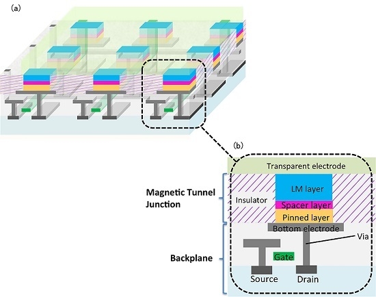
2.1. Structure and Operation of the Spin-SLM

Figure 1 shows a schematic and a cross-sectional illustration of the spin-SLM. Magnetic tunneling junctions (MTJs) include light modulation (LM) layers placed on top of the metal-oxide-semiconductor field-effect transistor (MOSFET). An MTJ is fabricated on the bottom electrode, which is then connected to the MOSFET. The drain and transparent electrodes are connected to the bottom and top surfaces of the MTJ element, respectively.
Figure 2a shows a schematic illustration of a circuit diagram for spin-SLM. We designed a 100 × 100 MOSFET array with 2 μm × 2 μm pixel pitch transistor dimensions. Resistance symbols indicate MTJ devices. We inject current into the MTJs and switch the magnetization of the LM layer by turning on a pixel- and row-selection-transistor. Each row and column driver consisted of ten pairs of 10-bit serial-in parallel-out shift registers. As shown in Figure 2b, input serial data was sequentially shifted by a clock signal, and was converted to output parallel data by a latch signal. Because one shift resistor was able to select ten rows or columns, the number of terminals required decreased by nine-tenths, which is significantly important for expanding pixel format into large scale.
This pulsed driving current was defined by the drain current, and Figure 3 plots the drain current versus voltage characteristics of transistors with 2 or 5 μm pixel pitches. The on-state resistances of these transistors at gate voltages of 3.3 or 1.2 V (as determined from this figure) were 86 Ω (5 μm) and 370 Ω (2 μm), respectively. Because the drain current was proportional to the transistor dimensions, it decreased as the transistor became smaller. Therefore, it was more difficult to drive the 2 μm spin-SLM compared to the 5 μm device.

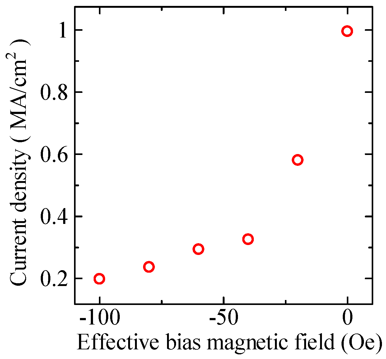
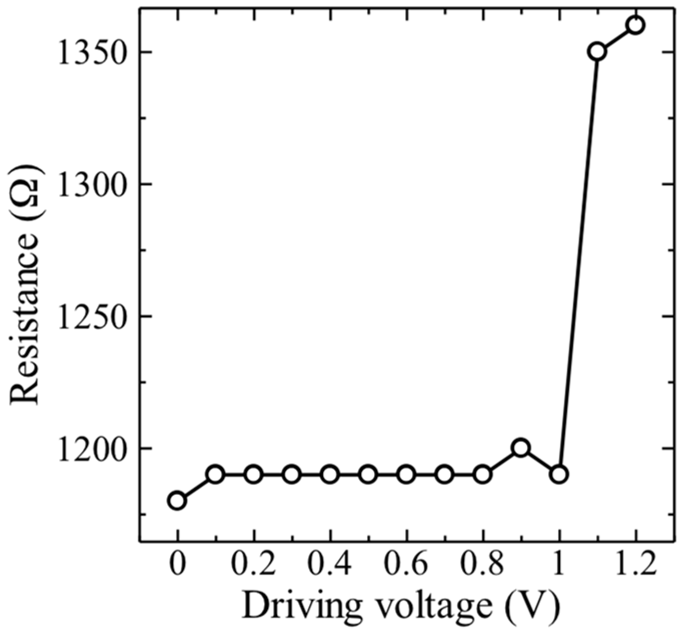
2.2. Magnetic Field-Assisted STS in MTJ Device

We have evaluated how an assisted magnetic field affects the STS current density (Jc) using an MTJ that has no pixel-selection-transistors, as shown in Figure 4. The evaluated MTJ device consisted of a pinned layer, an MgO insulating layer as a tunneling barrier, and an LM layer. The pinned layer uses an amorphous alloy (Tb–Fe–Co) in order to obtain a smooth surface, because the surface roughness strongly affects the properties of a MTJ. The MgO layer is sandwiched between the two Co–Fe layers, which is typical in MTJs [15]. An amorphous Gd–Fe alloy was employed in the LM layer, because this material is known for exhibiting a large magneto-optical (MO) effect. The data in Figure 4 demonstrate that Jc decreased with an increase in the magnetic field. Therefore, this method would be very effective for the spin-SLM with 2 µm pixel pitch, which has limited current supply capability.

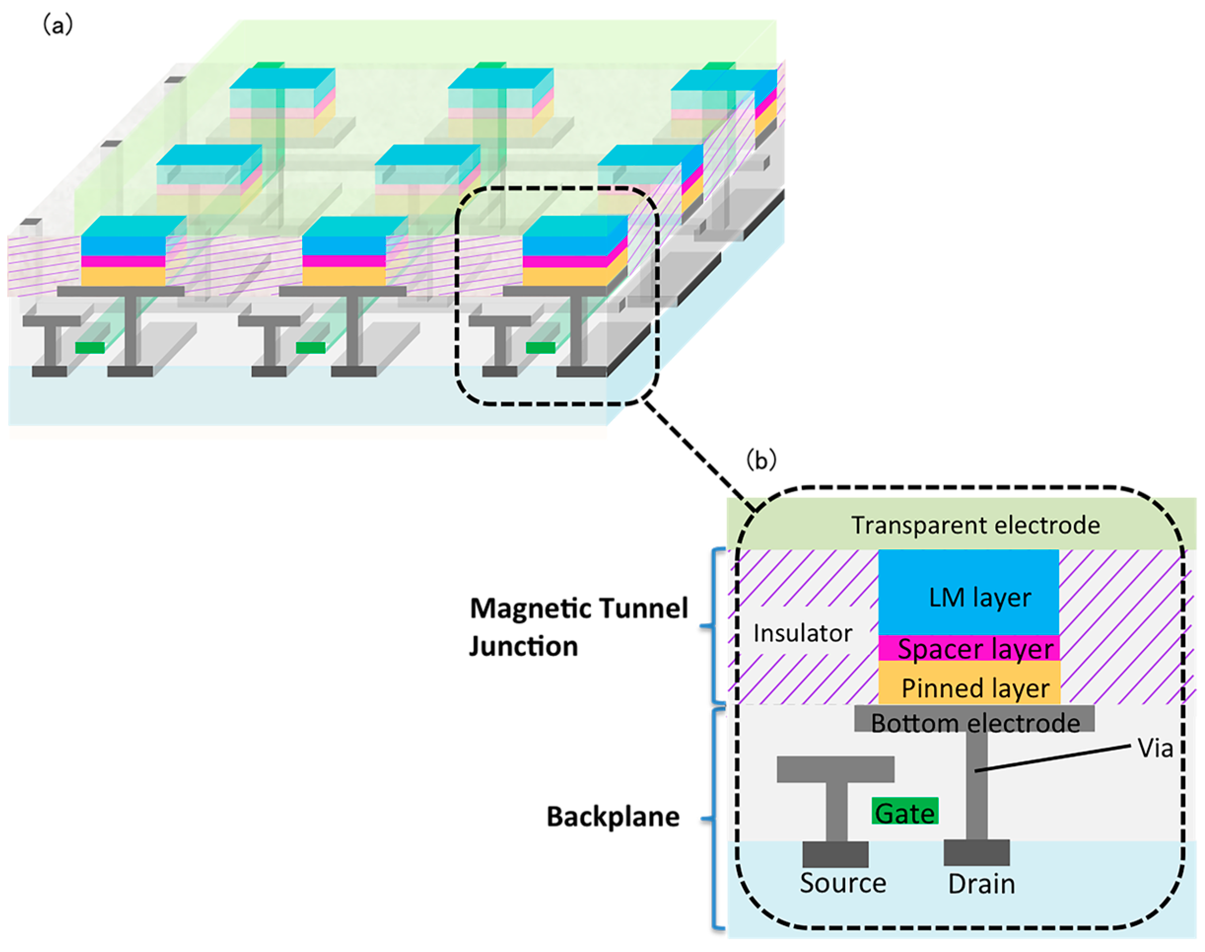
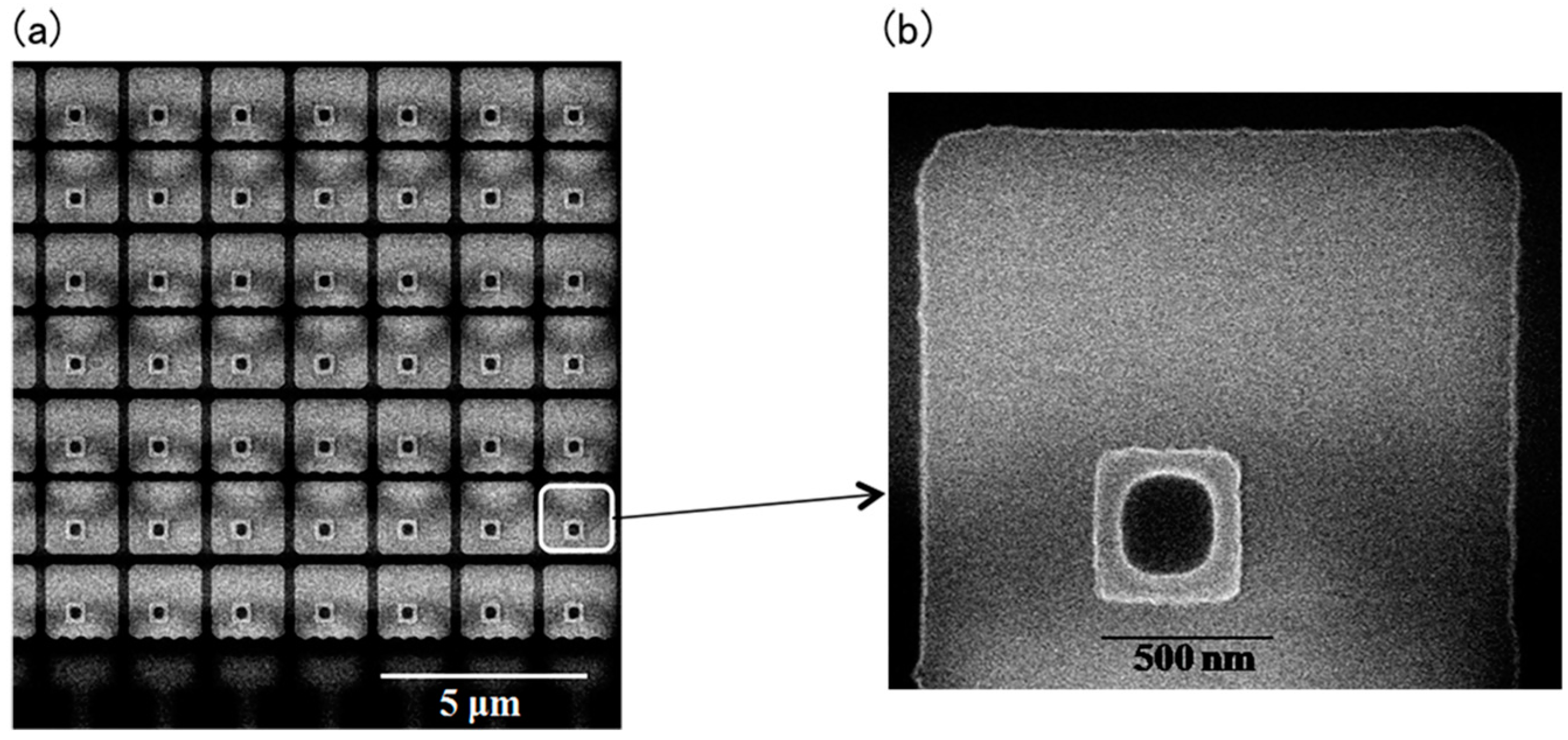
2.3. Fabrication of an Active Matrix Spin-SLM

The MOSFET backplane fabricated in this work comprised a 100 × 100 field-effect transistor (FET) array with a 2 μm pixel pitch. Each drain terminal of the FET was connected to the pinned layer of the MTJ through a copper electrode, each of which was composed of a 100 × 100 electrode array. The MTJ device consisted of a pinned layer of Ru (3 nm)/Tb–Fe–Co (10 nm)/Co–Fe (0.5 nm), a 1 nm MgO insulating layer, and an LM layer of Co–Fe (0.25 nm)/Gd (0.2 nm)/Gd–Fe (9 nm)/Ru (3 nm), which were all deposited using an ion beam sputtering system [13]. Because the 100 × 100 spin-SLM comprises a large number of pixels, it is very important to obtain uniform MTJ properties. Therefore, we chose to use a slightly thicker 1 nm MgO layer so as to obtain a more homogeneous tunneling barrier, rather than a 0.8 nm MgO layer (which was used in a 5 μm pixel pitch spin-SLM). Magnetic pixels were patterned by electron-beam (EB) lithography and etched via an ion milling process, and with an additional insulator deposition and liftoff process. Figure 5a,b present scanning electron microscopy (SEM) images of the bottom electrodes and the EB resist pattern before the ion milling process, respectively. We determined the device size by measuring the EB resist dimensions, as shown in Figure 5b. The size of each MTJ element was 470 nm × 470 nm, and each element was fabricated on a 1.76 μm × 1.76 μm bottom electrode. A transparent electrode structure consisting of indium zinc oxide (135 nm) was then deposited using ion beam sputtering [16,17].

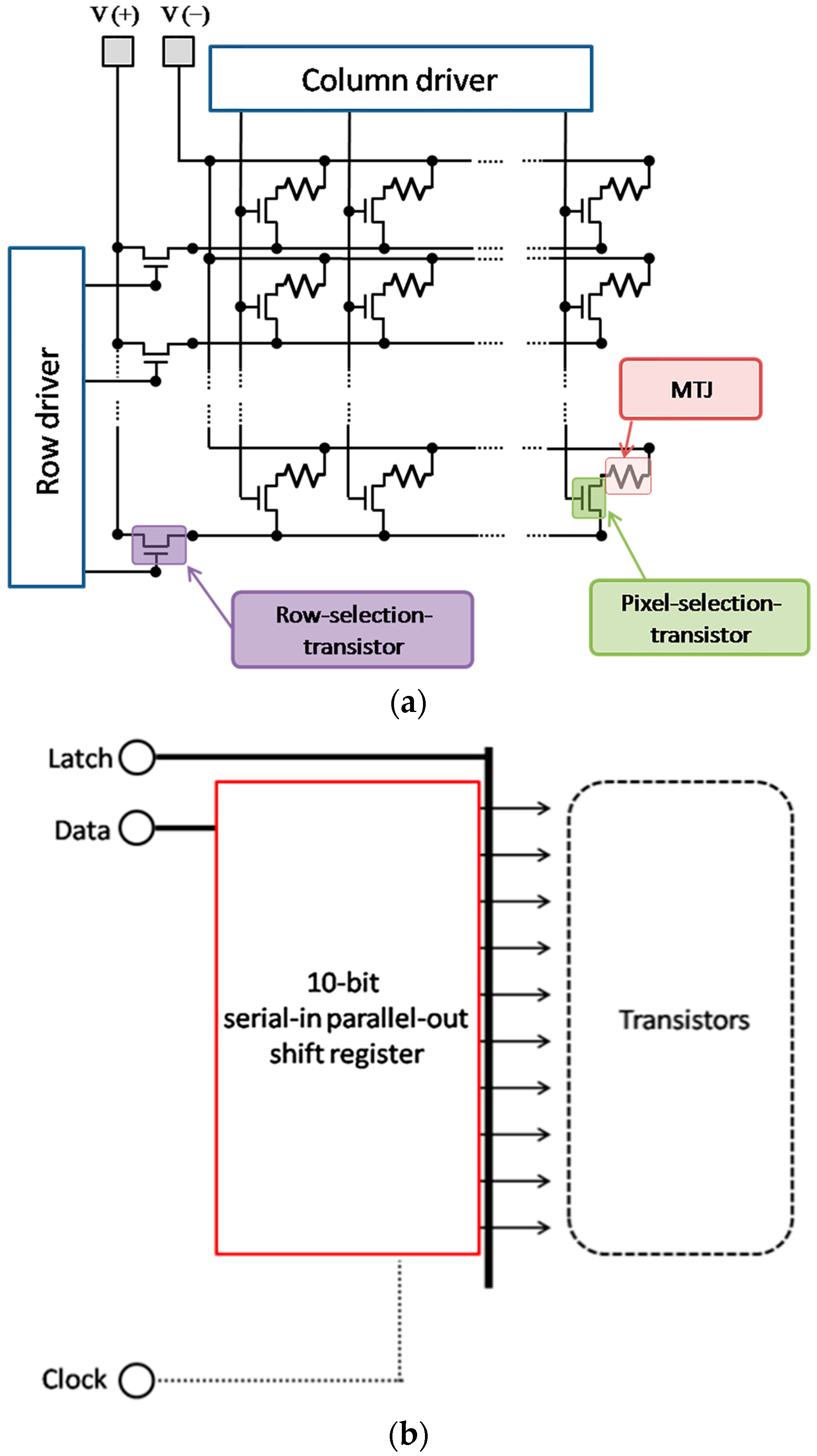
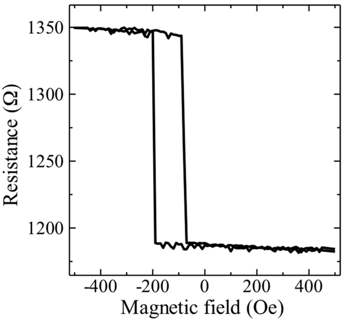
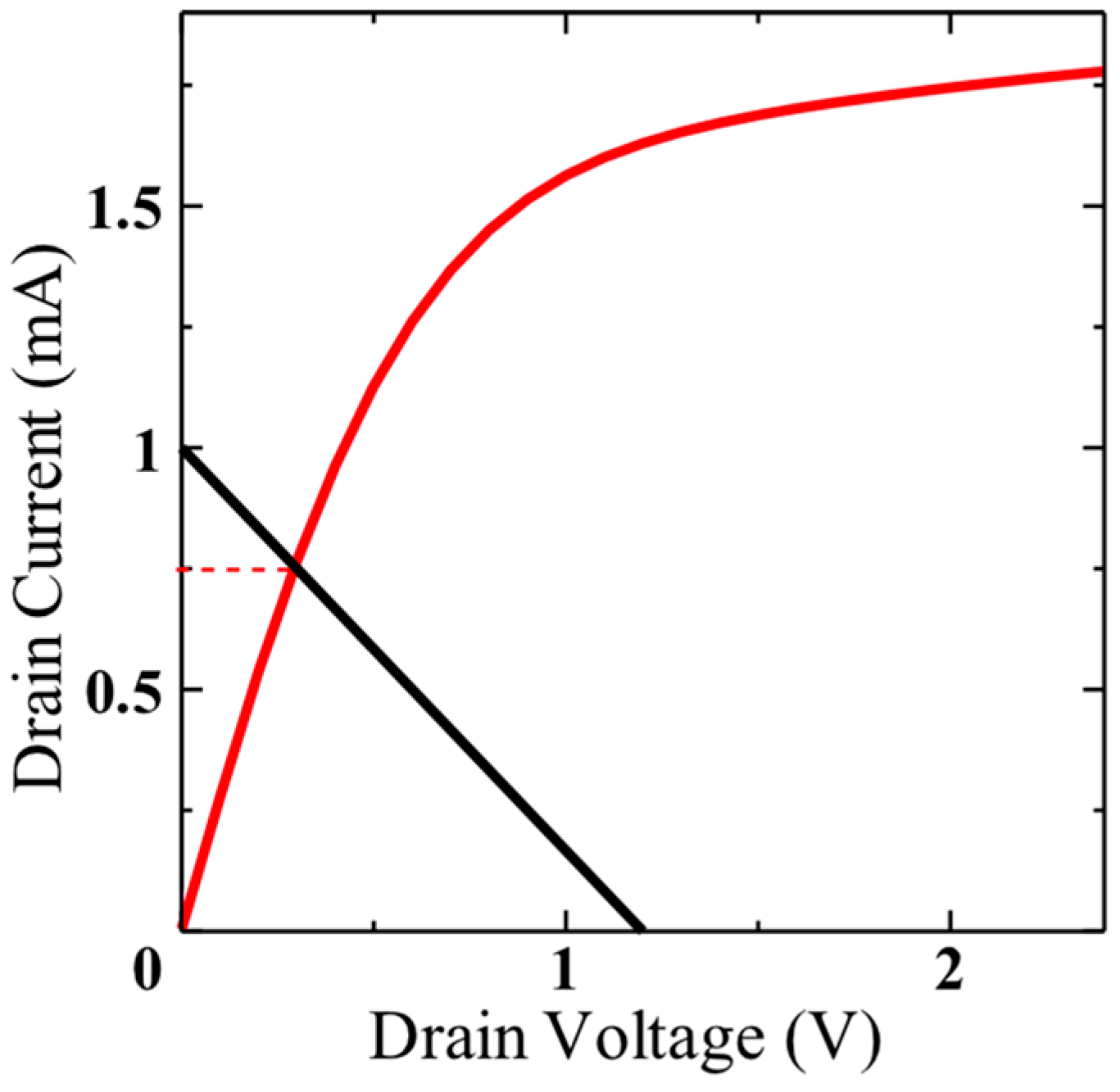
2.4. Electrical Characteristics of the Active Matrix Spin-SLM

The fabricated spin-SLM device was attached to a probe station with electromagnets and a controller driving unit for the shift registers and pixel-selection-transistors. Figure 6 presents the magneto-resistance (MR) loop of an LM layer in this device. The device resistance evidently varied as the magnetic field was swept, a behavior that is typical of an MTJ device. When the magnetization direction of the LM layer and the pinned layer were in parallel (P) and anti-parallel (AP) configurations, the device exhibited low and high resistance levels, respectively. The resistance values of the MTJ (excluding the transistor resistance) in the P and AP state were 1180 and 1350 Ω, respectively. Table 1 compares the dispersion of the resistance in 50 elements selected at random from the two types of spin-SLMs (with 5 μm and 2 μm pixel pitches). Standard deviation of the resistance distribution in the 2 μm pixel pitch device was approximately one-third of that of the 5 μm pixel pitch device. The uniformity of the device resistance is extremely important to drive all the pixels in the SLM, and it leads to uniformity of the injection current, since the backplane transistor only applies a voltage pulse. This reduction of deviation enabled the spin-SLM with larger pixel format to drive unfailingly. We attribute the improvement to fewer defects in the thicker MgO layer, with a speculation of thinner MgO tending to have more defects, resulting in larger resistance distribution. The switching magnetic fields associated with the P-to-AP and AP-to-P states were −200 and −70 Oe, respectively, while the loop center was shifted to −135 Oe in the negative magnetic field direction. We speculate that this shift was due to a magnetic leakage field originating from the pinned layer.
We estimated current supply produced by a pixel-selection-transistor with a MTJ. The drain current that was supplied to each MTJ device by the pixel-selection-transistor is described by Equation (2), which is based on Kirchhoff’s second rule.
I d = V D R + V R
Here Id is the drain current, VD is the drain voltage, R is the MTJ device resistance, and V is the driving voltage. In the case of the present study, R was 1180 Ω and V was 1.2 V. The drain current with the additional resistance of the MTJ was evaluated by determining the intersection point of Equation (2), and the transistor characteristics curve is shown in Figure 3. As displayed in Figure 7, the value of Id was 0.75 mA, which corresponds to 0.33 MA/cm2. In contrast, the required switching current density of the MTJ devices was 1.0 MA/cm2 [13], this being a much greater current density than the transistor could provide. For this reason, we employed magnetic field-assisted STS in conjuction with the 2 μm pixel pitch spin-SLM.
The STS characteristics were evaluated by applying 1 μs duration drain voltage pulses as the driving voltage. Figure 8 plots the resistance as a function of the driving voltage applied to an arbitrarily-selected LM element, with a bias magnetic field of −35 Oe from the loop center in Figure 6 to assist the STS. It can be seen that the resistance jumped from a low value to a high value at the driving voltage of 1.1 V, which corresponds to the magnetization switching of the LM layer from the P to the AP configuration. The magnetization reversal current determined from Figure 7 was 0.70 mA (0.32 MA/cm2). This was consistent with the results shown in Figure 4.

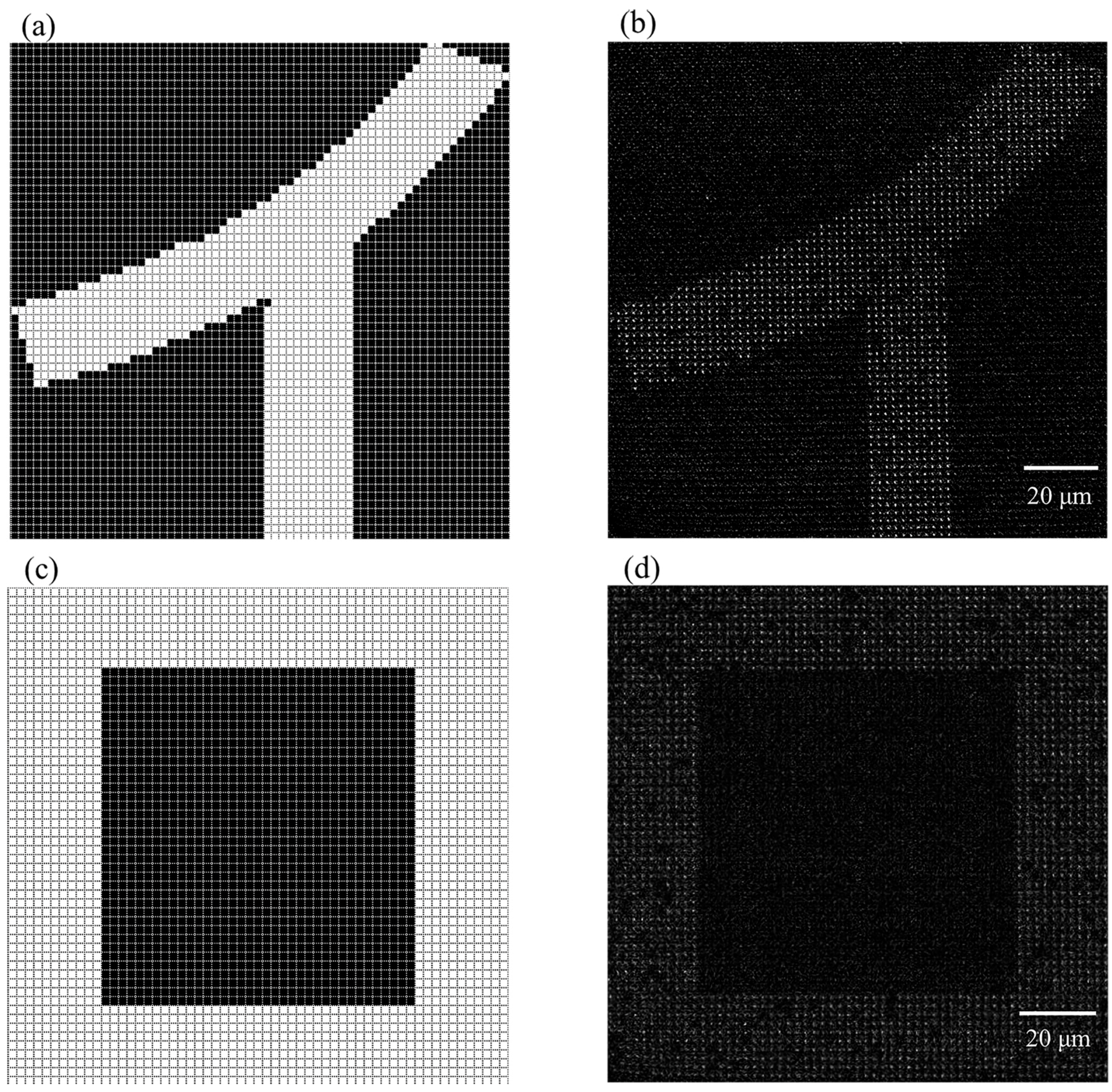
2.5. Magneto-Optical Properties of the Active Matrix Spin-SLM

We applied a magnetic field of 8.0 kOe to switch all of the 100 × 100 LM elements to the P-configuration. The field was subsequently decreased to −170 Oe (effective magnetic field of −35 Oe), and an initial MO was acquired under the conditions listed in Table 2. The wavelength of the light source was 463 nm. Following this, a driving voltage of 1.2 V was applied to the LM elements, corresponding to the white pixels in the bitmap images in Figure 9a or Figure 9c, and micrographs were again acquired. We then performed an image division operation between the MO photographic image taken after voltage application and that taken before voltage application. Figure 9b or Figure 9d shows the resulting division image. The LM elements that corresponded to the white pixels shown in Figure 9a or Figure 9c became brighter as a result of the magnetization switching. We saw some dark elements even after voltage application, which was not switched and was attributed to the pixel defects, which might require larger current or magnetic field. Although we have already demonstrated a reconstructed static image using a magnetic hologram with same magnetic materials used in the spin-SLM [14], the MO image contrast obtained by the MOSFET-driven spin-SLM was low and may not be sufficient for holographic image reconstruction. This is mostly because of the small aperture ratio of 5.5% (lateral size of the MTJ versus size of a pixel). Expanding the LM area requires a larger current to drive, since the STS is determined by current density. In order to obtain a better aperture ratio, we have to decrease switching current by increasing spin injection efficiency with highly spin polarized materials [18] or increasing the current supply capability of the backplane transistor. We are also considering the development of new techniques other than MTJ in which the switching current is independent of the element size. Although our current device may require more improvement, such as larger aperture ratio for realizing a holographic movie, the MOSFET-driven spin-SLM has shown the potential to expand its scale for larger pixel format.

3. Conclusions

We have fabricated an active matrix-driven spin-SLM composed of 100 × 100 pixels with 2 μm pixel pitch, which has logic circuits with shift registers in order to reduce input terminals and drive a large number of pixels. The number of terminals decreased to one-tenth by using ten pairs of 10-bit shift registers. We have successfully controlled the switching of individual pixels using improved LM elements with small resistance distribution, and confirmed the display capability of two-dimensional images. Although we need to enlarge the aperture ratio for better light modulation efficiency, we believe that the spin-SLM with shift resisters has an important role for the realization of large-scale spin-SLM.

Acknowledgments

This work was supported by the National Institute of Information and Communications Technology (NICT) in Japan, (program period: 2009–2016).

Author Contributions

Kenichi Aoshima, Nobuhiko Funabashi, and Takenobu Usui designed the experiments; Shintaro Aso performed the experiments; Daisuke Kato, Kenji Machida, Kiyoshi Kuga, and Hiroshi Kikuchi discussed the topic; Takayuki Ishibashi contributed analysis tools; Hidekazu Kinjo designed and performed the experiments and wrote the paper.

Conflicts of Interest

The authors declare no conflict of interest.

References

  1. Gabor, D. A new microscopic principle. Nature 1948, 161, 777–778. [Google Scholar] [CrossRef] [PubMed]
  2. Leith, E.N.; Upatnieks, J. Reconstructed wavefronts and communication theory. J. Opt. Soc. Am. 1962, 52, 1123–1128. [Google Scholar] [CrossRef]
  3. Senoh, T.; Mishina, T.; Yamamoto, K.; Oi, R.; Kurita, T. Viewing-zone-angle-expanded color electronic holography system using ultra-high-definition liquid crystal displays with undesirable light elimination. J. Disp. Technol. 2011, 7, 382–390. [Google Scholar] [CrossRef]
  4. Psaltis, D.; Paek, E.G.; Venkatesh, S.S. Optical image correlation with a binary spatial light modulator. Opt. Eng. 1984, 23, 698–704. [Google Scholar] [CrossRef]
  5. Mok, F.; Diep, J.; Liu, H.; Psaltis, D. Real-time computer-generated hologram by means of liquid-crystal television spatial light modulator. Opt. Lett. 1986, 11, 748–750. [Google Scholar] [CrossRef] [PubMed]
  6. Hashimoto, N.; Morokawa, S.; Kitamura, K. Real-time holography using the high-resolution LCTV-SLM. Proc. SPIE 1991, 1461. [Google Scholar] [CrossRef]
  7. Sonehara, T.; Miura, H.; Amako, J. Moving 3D-CGH reconstruction using a liquid crystal spatial wavefront modulator. In Proceedings of the 12th International Display Research Conferences, Hiroshima, Japan, 12–14 Octobre 1992; p. 315.
  8. Takaki, Y.; Hayashi, Y. Increased horizontal viewing zone angle of a hologram by resolution redistribution of a spatial light modulator. Appl. Opt. 2008, 47, D6–D11. [Google Scholar] [CrossRef] [PubMed]
  9. Mishina, T.; Okui, M.; Okano, F. Viewing-zone enlargement method for sampled hologram that uses high-order diffraction. Appl. Opt. 2002, 41, 1489–1499. [Google Scholar] [CrossRef] [PubMed]
  10. Aoshima, K.; Funabashi, N.; Machida, K.; Miyamoto, Y.; Kawamura, N.; Kuga, K.; Shimidzu, N.; Sato, F.; Kimura, T.; Otani, Y. Spin transfer switching in current-perpendicular-to-plane spin valve observed by magneto-optical Kerr effect using visible light. Appl. Phys. Lett. 2007, 91. [Google Scholar] [CrossRef]
  11. Aoshima, K.; Funabashi, N.; Machida, K.; Miyamoto, Y.; Kuga, K.; Ishibashi, T.; Shimidzu, N.; Sato, F. Submicron magneto-optical spatial light modulation device for holographic displays driven by spin-polarized electrons. J. Disp. Technol. 2010, 6, 374–380. [Google Scholar] [CrossRef]
  12. Aoshima, K.; Machida, K.; Kato, D.; Mishina, T.; Wada, K.; Cai, Y.; Kinjo, H.; Kuga, K.; Ishibashi, T.; Kikuchi, H.; et al. A magneto-optical spatial light modulator driven by spin transfer switching for 3D holography applications. J. Disp. Technol. 2015, 11, 129–134. [Google Scholar] [CrossRef]
  13. Kinjo, H.; Machida, K.; Matsui, K.; Aoshima, K.; Kato, D.; Kuga, K.; Kikuchi, H.; Shimidzu, N. Low-current-density spin-transfer switching in Gd22Fe78-MgO magnetic tunnel. J. Appl. Phys. 2014, 115. [Google Scholar] [CrossRef]
  14. Aoshima, K. Magneto-optical spatial light modulator driven by Si based MOSFET backplane for holography display. In Proceedings of the 21st International Display Workshops, Niigata, Japan, 3–5 December 2014; pp. 1247–1258.
  15. Yakushiji, K.; Noma, K.; Saruya, T.; Kubota, H.; Fukushima, A.; Nagahama, T.; Yuasa, S.; Ando, K. High magnetoresistance ratio and low resistance–area product in magnetic tunnel junctions with perpendicularly magnetized electrodes. Appl. Phys. Exp. 2010, 3. [Google Scholar] [CrossRef]
  16. Goto, S.; Tang, S.; Aoshima, K.; Machida, K.; Kuga, K.; Kikuchi, H.; Shimidzu, N.; Ishibashi, T. Simulation of magneto-optical properties of GMR structures for SLM. In Proceedings of the 59th Spring Meeting of the Japan Society of Applied Physics, Tokyo, Japan, 15–18 March 2012; pp. 10–100.
  17. Goto, S.; Machida, K.; Aoshima, K.; Kuga, K.; Kikuchi, H.; Shimidzu, N.; Ishibashi, T. Magneto-optical properties of (Pt/Co)/X/IZO (X = Ta, Au, Pt, Ru, and Ag) structures for magneto-optical light modulator. EPJ Web Conf. 2013, 40. [Google Scholar] [CrossRef]
  18. Diao, Z.; Apalkov, D.; Pakala, M.; Ding, Y.; Panchula, A.; Huai, Y. Spin transfer switching and spin polarization in magnetic tunnel junctions with MgO and AlOx barriers. Appl. Phys. Lett. 2005, 87. [Google Scholar] [CrossRef]
Figure 1. (a) Schematic and (b) cross-sectional illustration of the magneto-optical spatial light modulator (SLM) with submicron pixel sizes driven by spin-transfer switching (spin-SLM).
Electronics 05 00055 g001
Figure 2. (a) Schematic illustration of the circuit diagram for the spin-SLM; (b) Schematic illustration of the 10-bit shift register. MTJ: magnetic tunnel junction.
Electronics 05 00055 g002
Figure 3. Pixel transistor characteristics of transistors with dimensions of 5 μm × 5 μm (blue) and 2 μm × 2 μm (red).
Electronics 05 00055 g003
Figure 4. The current density, Jc, in an MTJ device as a function of magnetic field.
Electronics 05 00055 g004
Figure 5. SEM (scanning electron microscopy) images showing (a) a partial view; and (b) a single pixel from in the 2 μm pixel pitch spin-SLM.
Electronics 05 00055 g005
Figure 6. Magneto-resistance characteristics of the LM element in the spin-SLM.
Electronics 05 00055 g006
Figure 7. The transistor characteristics (red) and load line (black) of the 2 µm spin-SLM.
Electronics 05 00055 g007
Figure 8. Spin-transfer switching (STS) characteristics of the LM element in the 2 μm pixel pitch spin-SLM. (bias magnetic field: −35 Oe).
Electronics 05 00055 g008
Figure 9. (a,c) Input images; and (b,d) output images (MO imaging) from the spin-SLM.
Electronics 05 00055 g009
Table 1. Electrical characteristics of the two spin-SLMs.
Pixel Pitch of Spin-SLMs2 μm Pixel Pitch5 μm Pixel Pitch
MgO layer thickness1.0 nm0.8 nm
Average of resistance (arbitrarily selected)1150 Ω640 Ω
Standard deviation of resistance (arbitrarily selected)16.3 Ω47.5 Ω
Table 2. Conditions for the magneto-optical (MO) micrograph.
MagnificationExposure TimeIntegration
2000×0.1 s20 times

