1. Introduction
In recent years, New Space has emerged as a novel paradigm in non-terrestrial communications. In this new scenario, satellites and Unmanned Aerial Vehicles (UAVs) are designed and built in a more time efficient, more flexible, and cheaper way than in traditional space. For this reason, satellite components are included into chips instead of separate pieces of specific hardware. This procedure reduces time to market, boosts the flexibility and reconfiguration and lowers the price. However, it introduces important challenges in the design. In particular, the design and implementation of algorithms, protocols and systems must be developed in a single chip and FPGA becomes very attractive because of its hardware efficiency and power consumption [
1]. The Consultative Committee for Space Data Systems 130.1-G-1 (CCSDS 130.1-G-1) established several protocols and standards for satellite communications [
2]. Among them, the European Cooperation for Space Standardization (ECSS) series were developed for traditional telemetry, command and housekeeping. Although recently the standard ECSS-E-ST-50-01C [
3] has been superseded by ECSS-E-AS-50-21C Rev.1 [
4], which adopts CCSDS 131.0-B [
5], this standard has been very useful and it is still valid for recent developments. Moreover, most of the communications blocks will be valid for the new standard because it has backward compatibility. Thus, the study and implementation of the former standard is very important for new developments. Only slight differences with respect to the previous standard are included such as different length for scrambler and the Low-Density Parity-Check (LDPC) or turbo coding. However, some parts of the earlier standards are still relevant. Concatenated coding schemes that use Reed–Solomon and convolutional encoders are still common in older missions, technology demonstrators, and space platforms with limited resources. These setups value predictable performance, simple implementation, and reliability. Thus, our implementation is still valid and serve as base for future developments. Moreover, since the new standard has backward compatibility, some new missions with limited hardware capabilities still adopt the former standard.
The main changes introduced by the newer standard affect the channel coding stage. Other processing blocks like the Symbol Interleaver, BPSK modulation, framing, and data handling stay mostly the same. Because this design uses a modular architecture, these components do not depend on the coding scheme. They can be reused or adapted when adding new coding techniques like LDPC. This approach keeps the design useful and flexible for future CCSDS- and ECSS-compliant systems.
Nowadays, the space industry has been revamped thanks to the incorporation of novel technologies and applications such as small satellites [
6,
7], Internet of Things (IoT) satellites [
8], Very High Throughput Satellites (VHTS) [
9], flexible payloads [
10] and Artificial Intelligence (AI) [
11]. Recent progress in wireless communications includes work on distributed architectures, beamforming techniques, and intelligent reflecting surfaces [
12,
13]. Although these methods are used in different areas, they show how communication system design continues to develop.
The traditional satellite industry relies on Geostationary Earth Orbit (GEO) satellites. These large satellites have several advantages but also some drawbacks for the current industry, namely, they are very expensive, the production cycle is extremely large, the launching process is more expensive, they need large antennas and transmit powers, the delay is huge for interactive, real-time or voice services, and robustness depends on the redundancy on board. In order to deal with these issues, we turn to Low Earth Orbit (LEO) satellites and other non-GEO elements [
14]. These satellites are much smaller than GEO counterparts; examples include cubesats or even picosats. Since the coverage area is smaller in comparison to GEO, a constellation design is used to provide the service [
15].
It is worth mentioning that most of the technologies introduced above need a sort of software-defined radio element in some of the parts of these satellites to be able to manage flexible payloads or services. In addition, they need to deal with satellite swarms or incorporate AI techniques. Thus, there has been an increasing trend in the implementation of algorithms on FPGA for LEO satellites, thanks to the benefits that the integration of Systems on Chip (SoC) and FPGA technologies have brought into a single embedded device [
16], for example, low power consumption, less hardware usage, and high data transmission speeds with higher bandwidth. We can refer to the Xilinx Zynq
® UltraScale+™ Radio Frequency System-on-Chip (RFSoC) device, which provides an essential advance in the performance of satellite communication systems [
17]. Its main benefits are that it includes Analog to Digital Converters (ADCs) and Digital to Analog Converters (DACs) converters, soft-decision forward error correction (SD-FEC) kernels, high-performance programmable logic, and an ARM
® multiprocessing system.
As indicated earlier, every satellite, independently on their application, must be equipped with the Telemetry, Tracking and Command (TTC) system for transmitting the data from satellite, to send commands to it and to know their position and status (housekeeping). For those purposes, the standard ECSS-E-ST-50-01C was defined [
3]. The research into adaptive channel coding schemes has increased, thus improving the efficiency and security of transceivers. This generated the implementation of 4G/5G communication networks on LEO satellites, which offer higher data rates, better performance, and lower implementation costs [
18]. As a consequence, the launch of LEO satellites is experiencing an exponential increase in recent years [
19], and the forecast is even more optimistic. For example, the SpaceX satellite constellation Starlink is composed of almost seven thousand active satellites, and the incoming Kuiper constellation will be composed of more than three thousand, among others.
To the best knowledge of the authors, few studies have been published on the implementation of the ECSS-E-ST-50-01C standard. For example, in [
20], the authors proposed the design for the Reed–Solomon encoder alone on an FPGA platform. Their design achieved a high data rate of 1.2 Gbps and a coding gain of 4.5 dB. In [
21], the authors developed a generic Software Defined Radio (SDR) implementation of a fully integrated Telemetry and Telecommand unit for CCSDS standard on an embedded dual-core ARM-based platform, which achieved a data rate of 200 Mbps. Despite these achievements, both studies suffer from limited data rates and the need for additional hardware or software.
Recent studies have examined satellite communication systems built on programmable hardware platforms, especially using FPGA -based designs and SDR architectures [
22,
23,
24]. These methods permit flexible, high-performance systems, particularly for channel coding and adaptive transmission schemes [
22,
23]. Most current research focuses on specific parts of the transmission chain, such as convolutional encoding, Viterbi decoding, and other channel coding blocks, rather than offering a complete solution [
23]. In addition, SDR -based methods often depend on software processing, which may not take full advantage of the parallelism and real-time features of modern FPGA hardware [
24]. Still, there is no complete, high-speed FPGA-based implementation of the full CCSDS/ECSS telemetry transmission chain in the literature. The parallel design of the whole system, the interdependence among blocks and the global optimization from the point of view of resources, data rate, and flexibility makes this paper useful for future designs.
In this paper, the goal is not to introduce a new coding standard, but to design and build a high-performance, resource-efficient FPGA architecture for telemetry transmission systems. This design uses a proven coding chain as a reference and focuses on modularity, scalability, and hardware efficiency. As a result, it can serve as a solid foundation for more complex or future communication systems. A new efficient design and implementation of the ECSS-E-ST-50-01C transmitter using Xilinx’s Zynq® UltraScale+™ RFSoC platform is proposed and analyzed. Our method supports high-throughput operation and can reach data rates up to 1.76 Gbps in fully parallel settings. It also improves coding performance and lowers hardware complexity and power use compared to previous approaches.
The use of RFSoC in LEO satellites has generated new areas of research based on integrated systems on a single chip. This way, the weight and size are reduced and, at the same time, we can protect from radiation with stronger and thicker elements because the area is usually smaller than in conventional modeling. Moreover, it allows stronger redundancy, what means more robust systems, because, basically, the whole system can be replicated several times in different chips (or even inside the same chip). A good example is the Madrid Flight on Chip (MFOC) project [
25]. In [
26,
27], by the authors, a different standard CCSDS 131.2-B-1 [
28] for high data rate is implemented on ZCU111 [
29] evaluation board compatible with LEO satellites. This standard is mainly based on turbo coding. Although this standard is in general more complex than the ECSS-E-ST-50-01C, the latter is more commonly used in real missions and it needs to be implemented more efficiently in order to save as much resources as possible for the rest of the system.
Our proposal here differs and stands out from the works previously mentioned [
20,
21] because it acts as a modern and configurable platform. In addition, the modules have been optimized for efficiency in both the data rate and the space. Remember that the implementation in a single chip imposes that everything is implemented in the same chip, which has limited capacity, space and power consumption. The communication part is one of the critical subsystems but, at the same time, it needs to use the minimum amount of resources because the instruments that generate the payload would use most of those resources. At the end of the day, the satellite is built for that. Thus, any optimization in space in the TTC is highly appreciated.
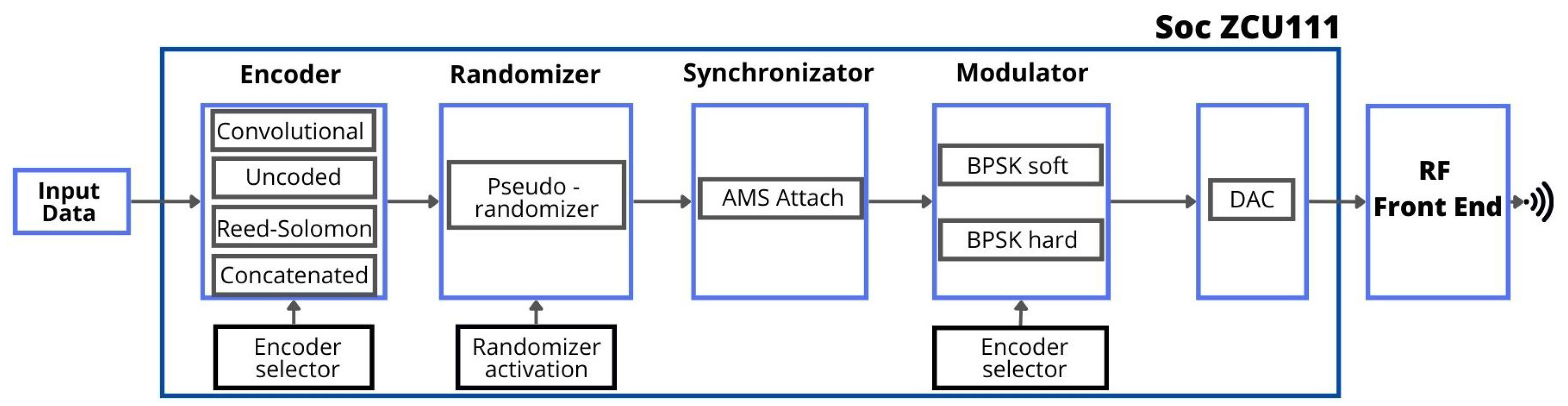
The main feature of our proposal is that it allows data to be transmitted in real-time and to configure the type of encoding on the fly. Thus, the transmitter adapts to the communication channel depending on the existing noise. To carry this out, the following codes were implemented in the FPGA image as the standard indicates: Convolutional, Reed–Solomon, Concatenated, and Uncoded. In addition, other blocks defined in the ECSS standard were also implemented, such as the pseudorandomizer which can be activated or deactivated on the fly. In addition, it can detect a new frame with the frame synchronization code block and has available two Binary phase shift keying (BPSK) modulator types soft and hard decision. The modulation type is defined by the selected encoder. All of this makes it the most flexible and versatile solution for satellite communication.
Moreover, since the blocks implemented are common for several standards, they could be reused and adapted to other systems, which makes this paper even more valuable.
In this context, the main contribution of this work consists of the design and implementation of a complete end-to-end telemetry transmission architecture based on the CCSDS 130.1-G-1 standard, fully implemented on an FPGA platform. In contrast to previous approaches that focus on isolated functional blocks, this work integrates Reed–Solomon encoding, convolutional coding, symbol interleaving, pseudo-randomization, and BPSK modulation into a unified and enhanced hardware architecture. Furthermore, the proposed design achieves high-throughput operation in the Gbps range while continuing productive resource utilization and meeting strict timing constraints on a Xilinx Zynq UltraScale+ RFSoC device. This demonstrates the feasibility of deploying high-performance telemetry transmitters in compact and power-efficient platforms suitable for small satellite and LEO communication systems. Additionally, this paper presents a detailed hardware-level analysis of resources usage, timing performance, and power consumption, providing a practical, reproducible reference design for future FPGA-based satellite communication systems. In summary, the key contributions of this work are:
- -
A complete end-to-end FPGA-based implementation of the CCSDS 130.1-G-1 telemetry transmission chain.
- -
A high-throughput architecture capable of achieving Gbps data rates on RFSoC platforms.
- -
An optimized hardware design with a detailed evaluation of resource utilization, timing performance, and power consumption.
This work does not focus on just one standard version. Instead, it examines hardware architecture, implementation methods, and ways to improve the performance of telemetry channel coding systems on FPGA platforms. While newer standards use advanced coding techniques, it is still important to make classical concatenated schemes more efficient for many space missions and as foundations for future coding systems. The proposed design is applicable to multiple standards and offers insights that apply to both current and future CCSDS-compliant systems.
The rest of this paper is organized as follows: the ECSS-E-ST-50-01C transmitter structure is presented in
Section 2. The FPGA implementation of the telemetry synchronization and coding blocks are explained in
Section 3. The measurement-based analysis and experimental results are included in
Section 4 and the conclusions are in
Section 5.
3. System Design
As explained eralier, the transmitter system has been implemented at the ZCU111 device, which is based on an RFSoC platform. This board has a powerful Processing System (PS) and Processing Logic (PL) with Arm
® Cortex
®-A53 and Arm Cortex-R5 subsystems. It is appropriate for our application because it has a comprehensive RF Analog to Digital signal chain prototyping platform which includes 8 12-bit 4.096 Giga Samples per Second (GSPS) ADCs, 8 14-bit 6.554 GSPS DACs, and 8 SD-FEC [
29].
We developed IP-Blocks [
32] in Very High Speed Integrated Circuit Hardware Description Language (VHDL) to have a cascading interconnected modular system. The intercommunication between the IP-Blocks uses the AXI4-Stream protocol [
33]. This standard is ideal for on-chip communications. It works based on handshake signals that indicate if the input or output data is valid and also if it is ready to receive or transmit the data. Based on this, we set 32 bits as the data width and 110 MHz as the frequency operation of all the IP-Blocks.
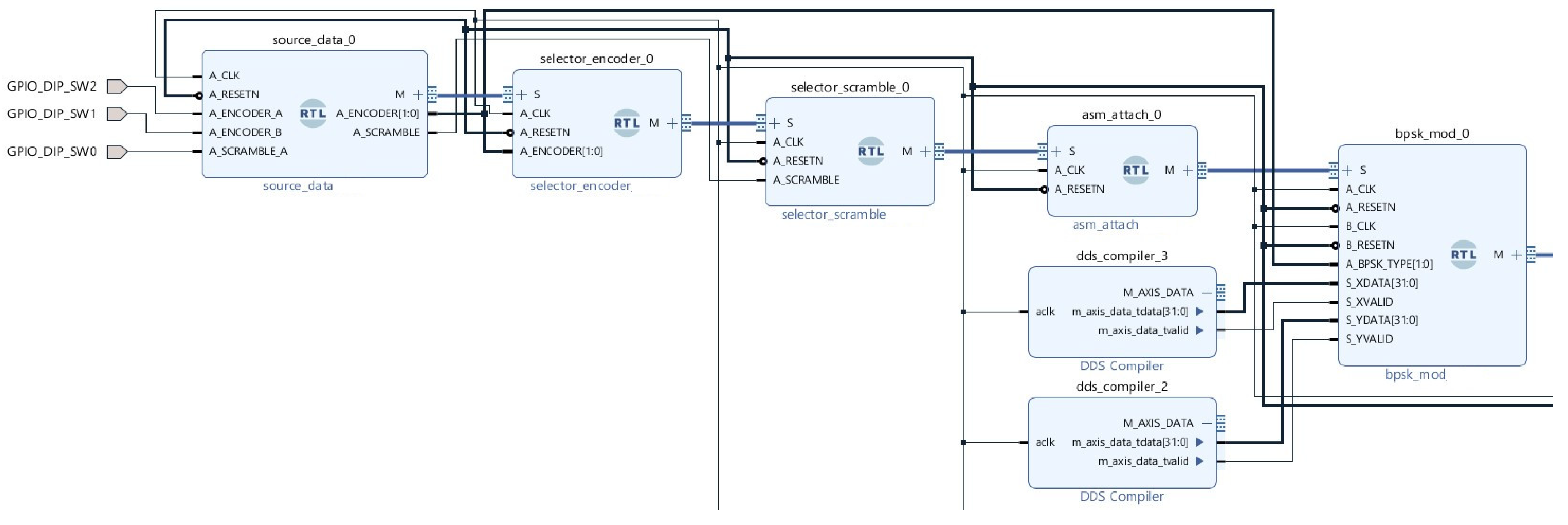
Figure 4 represents the transmitter block design, and how each IP-Block was interconnected following the standard [
3] implementation.
Next, we present a high-level overview of the coding processing tasks to encode, scramble, synchronize, and modulate the transmitter paths established by the CCSDS 130.1-G-1 standard [
30].
3.1. Encoder Selector
The encoder selector block serves as the initial encoding process for the input data.
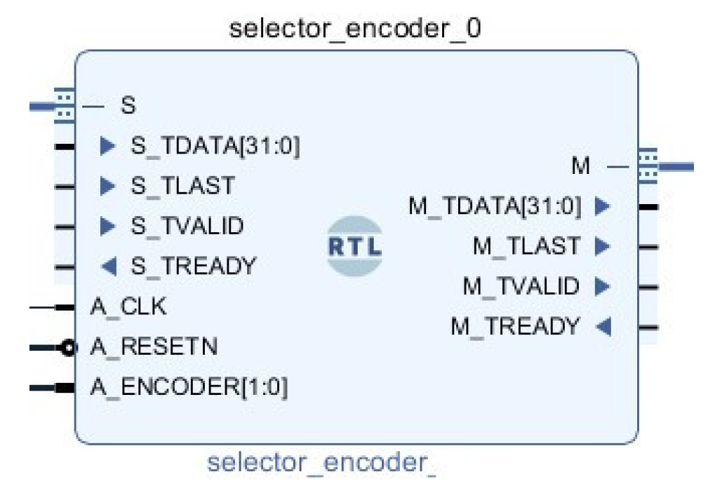
Figure 5 presents the IP encoder selector block, where input and output signals are shown. The main input signals are
A_ENCODER for selecting the desired encoding method. It can be configured in real-time using the switches on the ZCU111 development board or via the packet header. Another important signal is
A_CLK for the clock signal, the
S_DATA for the input data to be encoded. Two more signals are highlighted here,
M_TREADY to alert to the block that all the input signals are ready to use and
S_VALID indicating the input signals are valid. This is specially important in variable length frames processing. Moreover, in multi time processing. Input data follows the sampling time of the user data while the output of the encoder will depend on the selected encoding scheme and the interleaved length. Consequently, one of the important synchronization output signals are the
S_TREADY and
M_TVALID signals to inform to the next block that all the output data are valid and ready to use. Finally, output encoded data is at
M_TDATA.
3.2. Uncoded
As its own name indicates, in this case, no encoding scheme is implemented. This mode is recommended to be used over a channel without noise or with high quality.
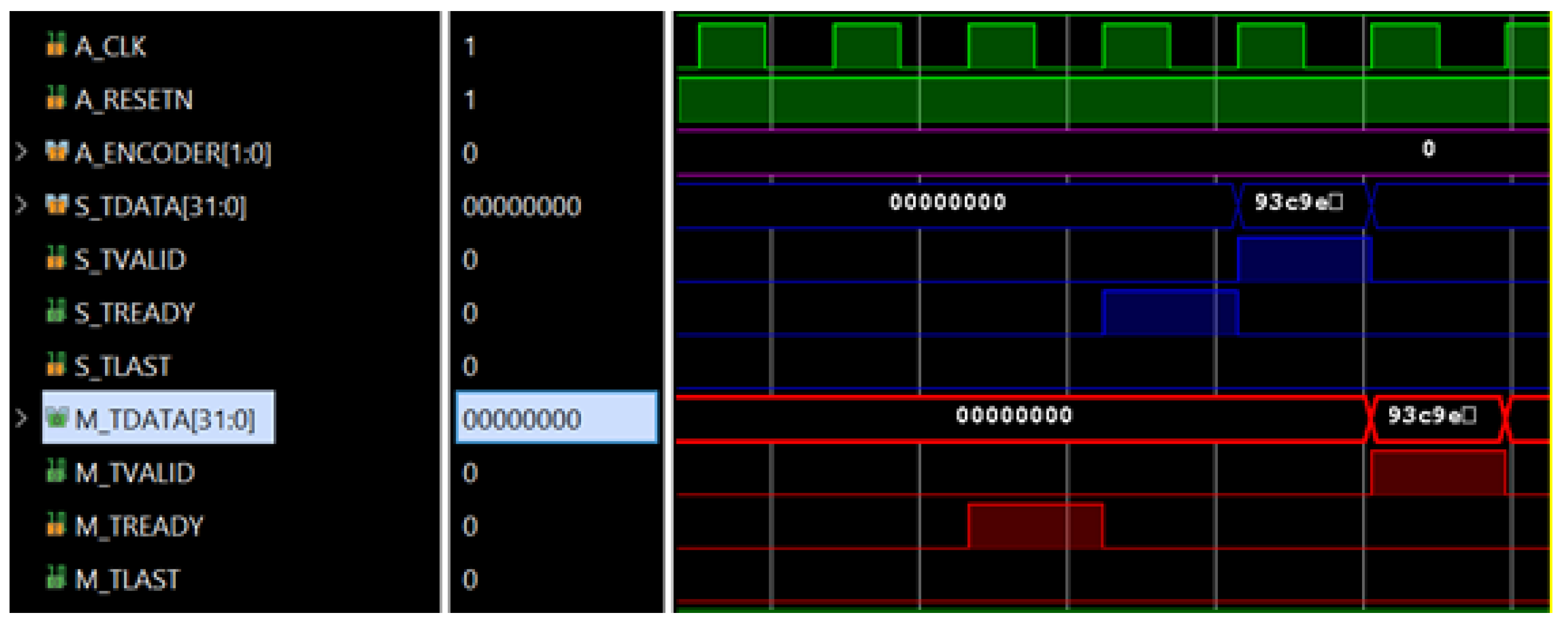
Figure 6 shows the simulation result, the output data is the same input data and it takes one clock cycle to finish the processing.
3.3. Convolutional Encoder
Convolutional codes have been widely implemented over the past decades to improve the reliability of communication channels in which the transmitted signal is corrupted by Additive white Gaussian noise (AWGN). Their effectiveness is largely due to their strong noise-rejection capability [
34].
According to the standard [
3], the convolutional coding scheme is defined by a code rate of
and a constraint length of 7 bits.
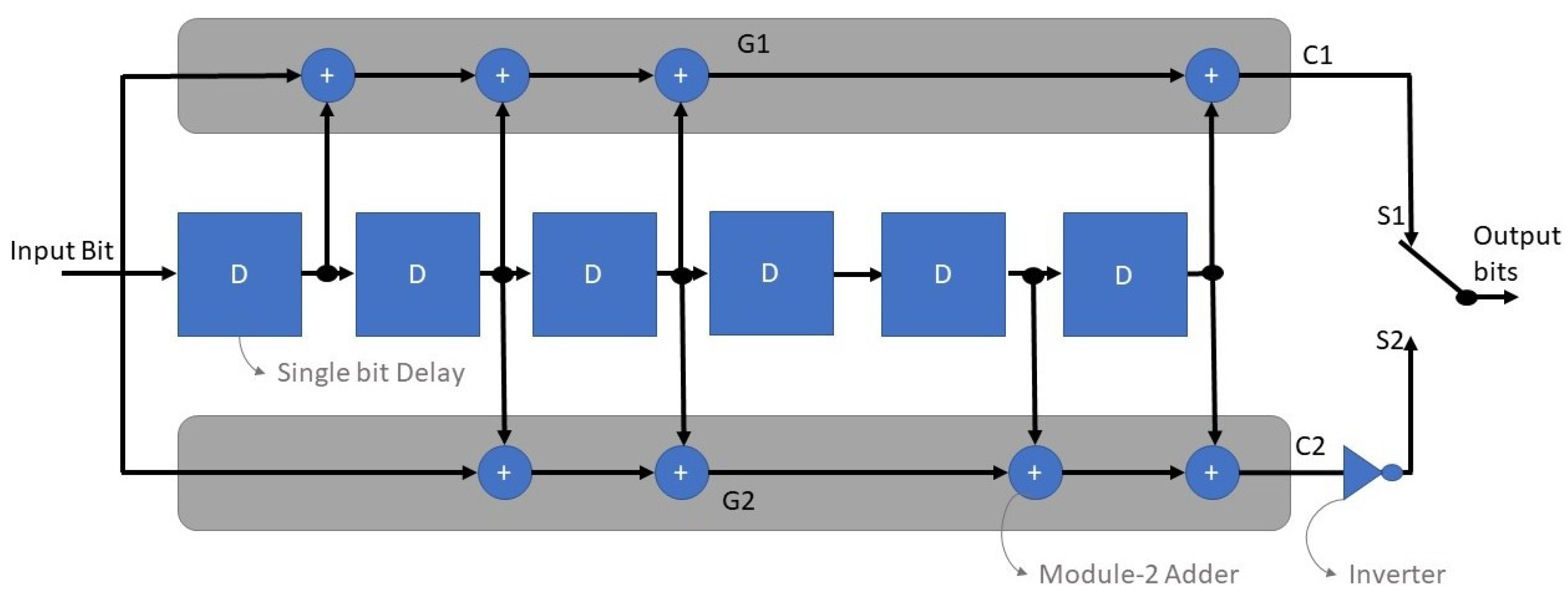
Figure 7 illustrates the block diagram of the convolutional encoder.
The operation of this encoding method is based on a set of delay elements connected to modulo-2 adders according to a predefined connection matrix. The delay elements temporarily store input bits, while the modulo-2 adders combine the stored bits to generate the encoded output bits. The specific structure and interconnections of these components are determined by the connection matrix of the convolutional encoder.
Figure 7 shows all the elements included in the convolutional encoder. The main characteristic is its memory, defined by a constraint length of 7 bits. The maximum free distance is the most important point in selecting the convolutional code parameters for the ECSS standard. After several trials, analysis, and simulations, a maximum free distance of
has been chosen to optimize the global performance.
The convolutional encoder can be described as the connection vector
for the branch and
for the lower one as follows
These two generator polynomials give two output bits for each input bit; thus, the code rate is
. These output bits can be obtained as
Figure 8 shows the detailed structure of the convolutional encoder to help explain the implemented architecture. The design uses a shift register approach for avoiding delays. Each input bit is processed one after another and combined with the internal memory states based on the generator polynomials.
Also, in
Figure 8 it can be seen that the encoder uses a six-stage shift register structure. It combines the current input bit with previous states using
XOR operations to produce the encoded outputs. The tap connections are set according to the used generator polynomials, ensuring the encoder operates as a proper encoder.
Each input bit is utilized to generate two coded bits, and . This results in a rate encoding scheme, where a 32-bit input word is transformed into a 64-bit encoded output. The encoded data is transmitted over the AXI4-Stream interface as two consecutive 32-bit output words. In order to only use a single cycle, they are transmitted in parallel.
The convolutional encoder algorithm was implemented following a systematic design approach. The input data are processed sequentially and encoded using predefined generator polynomials, while the encoder state is updated at each clock cycle. After the encoding stage, the resulting data are arranged appropriately for the subsequent stage of the transmission process.
The input data are encoded in parallel using a 32-bit input data package, implemented through carefully designed for loops. Although the use of loops in VHDL is generally discouraged for certain hardware descriptions, they can be safely and efficiently applied when properly structured, as in this implementation. In this design, the loops iterate through each bit of the input data and perform the corresponding encoding operations. The loop structures follow established hardware design principles, enabling an efficient hardware implementation.
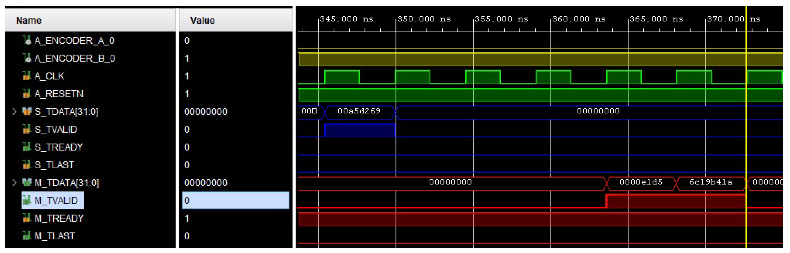
Figure 9 shows the simulation results of the convolutional encoder. The IP-Block receives a 32-bit input packet and produces two 32-bit output packets. The complete encoding process requires three clock cycles.
3.4. Reed–Solomon Encoder
The R-S code is an error-correction technique classified as a nonbinary block code. It protects transmitted data by introducing controlled redundancy into the original information, enabling the detection and correction of errors that appear during transmission. This approach is particularly well suited for satellite communication systems, where adverse environmental conditions such as atmospheric attenuation, interference, and burst noise are common.
The effectiveness of this coding scheme arises from its operation on symbols rather than individual bits, which allows it to efficiently handle burst errors. In addition, its high degree of flexibility enables the adjustment of redundancy levels and error-correction capability according to specific system requirements. Its strong performance in noisy environments helps reduce retransmissions and improves the overall efficiency of bandwidth usage [
35].
The CCSDS 130.1-G-1 standard [
30] recommends two Reed–Solomon codes with a codeword length of
symbols. The code implemented in this work has the following parameters: an information length of
, a minimum distance of
, and the capability to correct up to
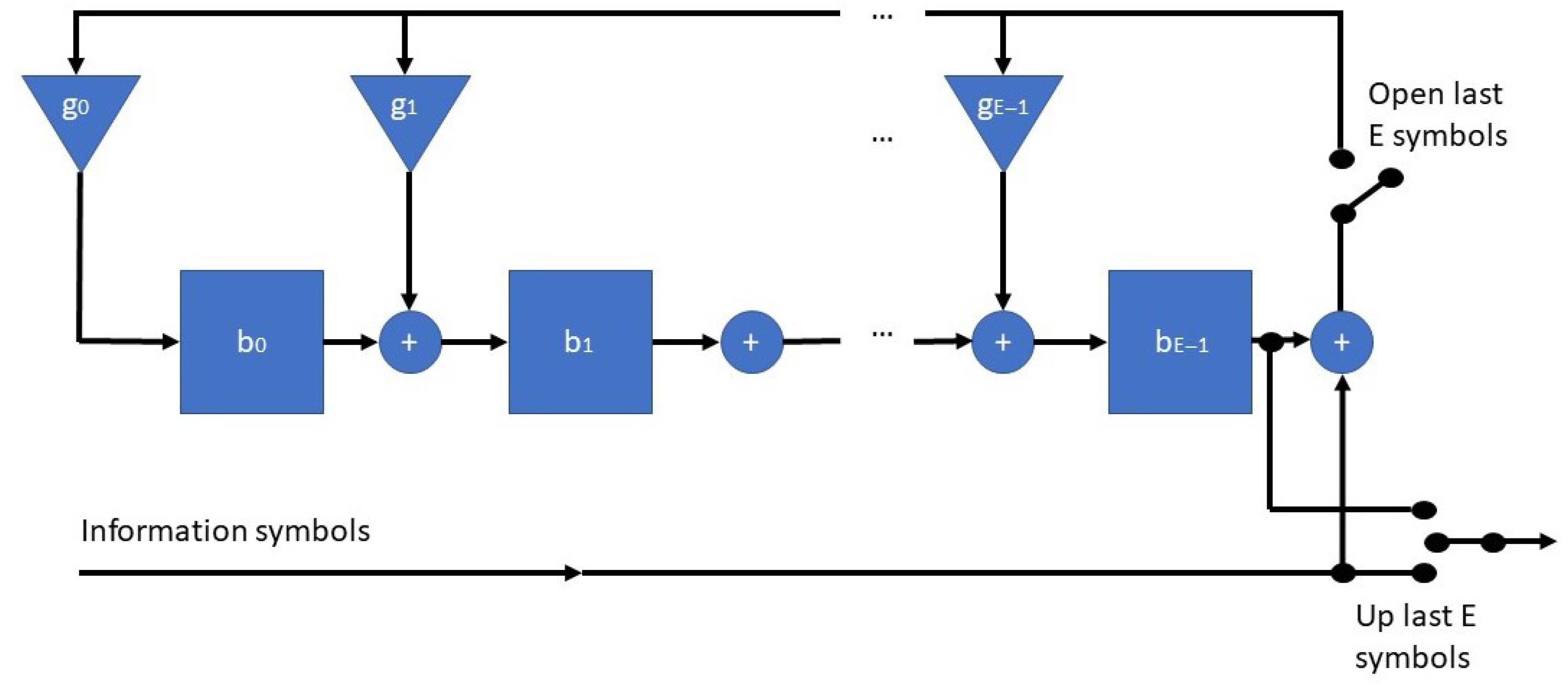
symbol errors. The block diagram of the R-S encoder is presented in
Figure 10. The R-S code has the field generator polynomial over
[
3]
The R-S code has the code generator polynomial over
, where
[
3]
Note:
is a primitive element in
.
While
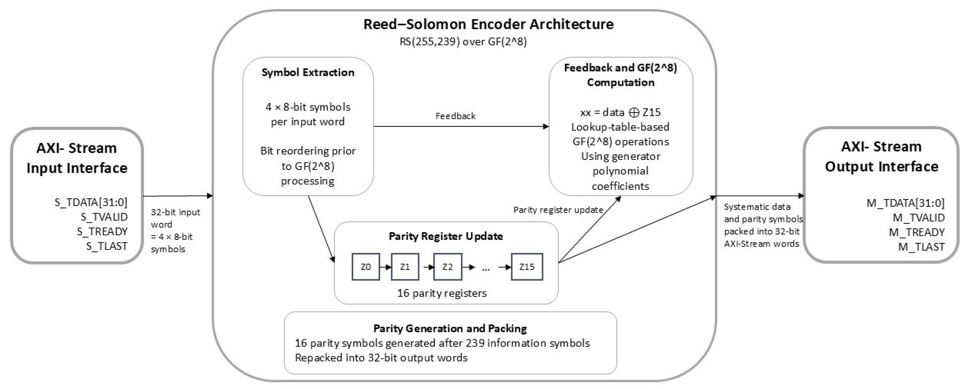
Figure 10 presents the conventional block diagram of a Reed–Solomon encoder, a more detailed view of the implemented hardware architecture is provided in
Figure 11. This representation highlights the internal processing stages and the specific design choices adopted in the FPGA implementation.
Figure 11 shows that the RS encoder operates with 32-bit AXI4-Stream input words. Each word is split into four 8-bit symbols, which are processed sequentially over
. The design employs a 16-stage parity register, corresponding to the 16 parity symbols of the RS(255,239) code. For each input symbol, a feedback value is computed using the current symbol and the last parity register. This value is then used in lookup table-based
operations to update the internal parity registers according to the generator polynomial coefficients. After processing 239 information symbols, the 16 parity symbols are generated and repacked into 32-bit words for transmission through the AXI4-Stream output interface.
The R-S encoder was implemented in VHDL and organized into three main parts: data reception, symbol-level encoding, and data transmission. The encoder works with 8-bit symbols in and uses precomputed lookup tables for Galois field operations and generator polynomial coefficients. By using stored values rather than real-time calculations, this method reduces computational complexity and makes the hardware more efficient. A structured parity register setup allows the system to generate parity symbols in an organized way and keep data moving smoothly.
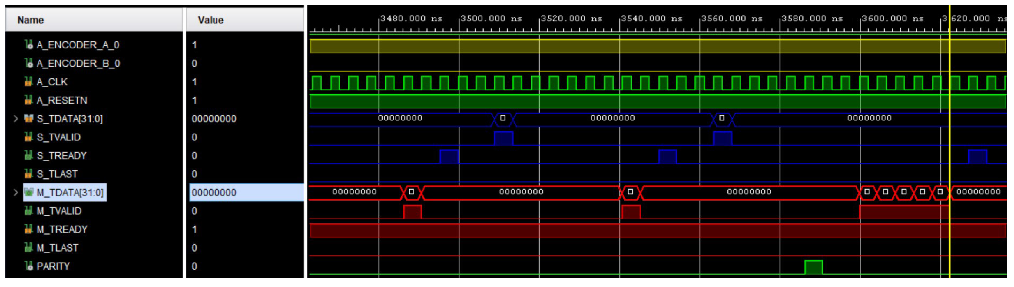
Figure 12 shows the simulation results of the R-S encoder, specifically in the stage where the parity symbols have already been computed. The implemented algorithm introduces a fixed delay of seven clock cycles between the input signal and the output. This delay is caused by the internal processing stages required to compute the parity symbols and prepare the encoded data. Once the parity calculation is completed, the parity symbols are transmitted sequentially, ensuring efficient delivery of the generated codeword.
The design was further optimized through the use of for loops, which enable repetitive operations—such as multiplications and modular additions in the Galois field (GF) —to be implemented in a compact and well-structured manner. This approach reduces hardware complexity and improves execution efficiency, as the loop indices directly control the iteration process and minimize processing overhead at each stage. As a result, the architecture achieves improved performance while maintaining a continuous flow of encoded data with minimal delay.
3.5. Concatenated Codes: Reed–Solomon and Convolutional
When the channel quality decreases to low levels, the concatenated coding architecture, with a R-S outer code and a convolutional inner code, is recommended by [
30], and aligns with [
3] requirements for space telemetry systems. The reason for this recommendation is rooted in the complementary error-correction properties of block and convolutional codes. Space communication channels are typically characterized by, namely, Low Signal-to-Noise Ratio (SNR), AWGN, Doppler shifts, Fading and synchronization losses and burst error events.
A single coding technique is typically inadequate for efficiently mitigating both random and burst errors in these scenarios. The concatenated structure overcomes this limitation by integrating two coding mechanisms that operate at distinct abstraction levels.
The outer code utilized in this study is the R-S code, as recommended in [
30]. With each symbol representing 8 bits, the R-S code is highly effective in correcting burst errors. It enables correct decoding even when up to eight symbols are corrupted, corresponding to as many as 64 consecutive bit errors distributed across symbol boundaries. R-S codes function at the symbol level, making them well suited for mitigating structured or burst-type channel impairments.
The inner encoder is implemented according to [
30]. The convolutional encoder produces two output bits for each input bit, utilizing the generator polynomials specified in the standard, commonly denoted as (171,133) in octal notation.
In contrast to R-S codes, convolutional codes operate at the bit level and are highly effective in correcting random errors introduced by thermal noise or AWGN channels.
However, convolutional codes alone are suboptimal for addressing long burst errors, as error propagation may surpass the decoder’s traceback capability. This limitation necessitates the use of serial concatenation with an outer RS code.
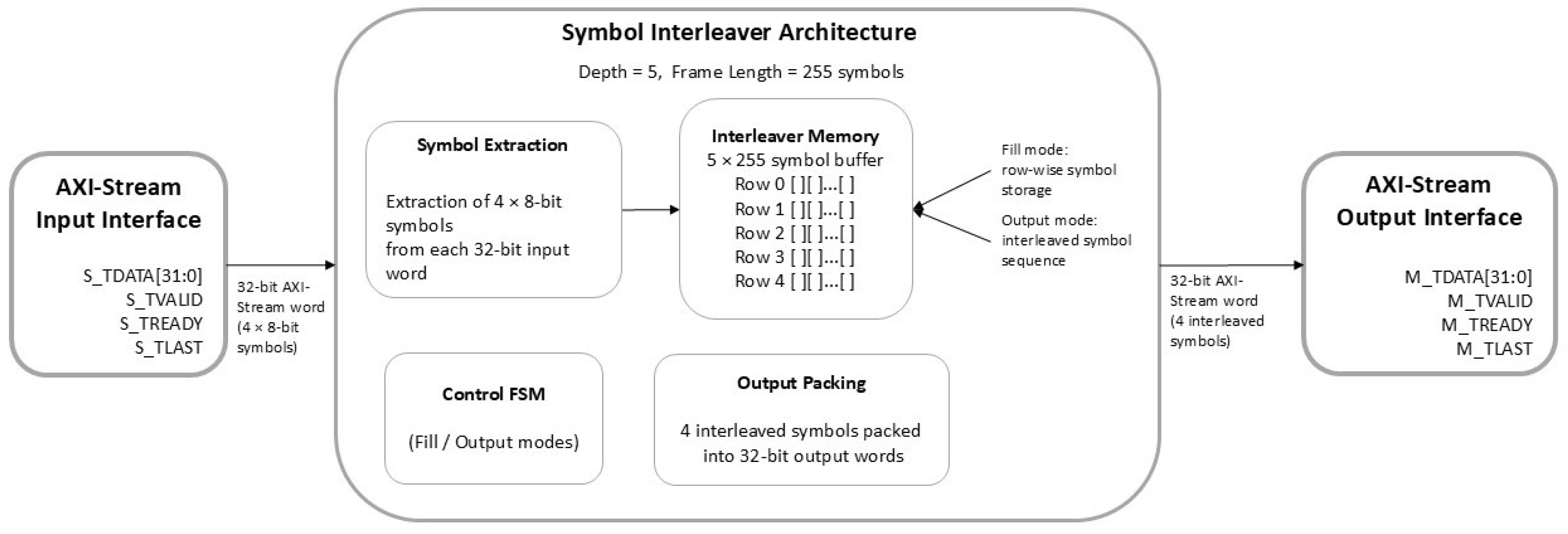
To enhance the effectiveness of the concatenated scheme, a block interleaver with depth is inserted between the R-S and the convolutional encoder.
The implemented interleaver writes RS codewords sequentially, row-wise, into memory and reads them column-wise for transmission. This approach distributes adjacent symbols from a single RS codeword across multiple transmitted segments.
The interleaving process transforms channel-induced burst errors into sparse symbol errors that are distributed across different RS codewords. Consequently, the effective burst length that can be tolerated increases by a factor approximately equal to the interleaving depth.
This architecture is particularly advantageous in environments with both random noise and burst-type impairments. The layered error protection strategy ensures that residual errors following convolutional decoding remain within the correction capability of the Reed–Solomon stage.
For these reasons, the RS–convolutional concatenated scheme is recognized as a classical and well-established solution in space communications.
The overall concatenated architecture implemented in this study is summarized in
Figure 13. The diagram shows how the outer R-S encoder, the Symbol Interleaver, and the convolutional inner encoder are arranged in series for transmission. It also shows the matching decoding steps at the receiver. This setup follows the layered error-control approach recommended by CCSDS 130.1-G-1 for space telemetry links.
As shown in
Figure 13, the proposed transmission chain uses a layered encoding strategy. The R-S encoder protects against burst errors, and the convolutional encoder helps guard against random errors. The Symbol Interleaver is important because it spreads burst errors across several codewords. This makes the combined scheme more effective. On the receiver side, the system applies the reverse operations in the reverse order to correctly recover the transmitted information. This architecture enables a flexible, robust transmission system that adapts to different channel conditions without requiring structural modifications.
3.6. Attached Synchronization Marker (ASM)
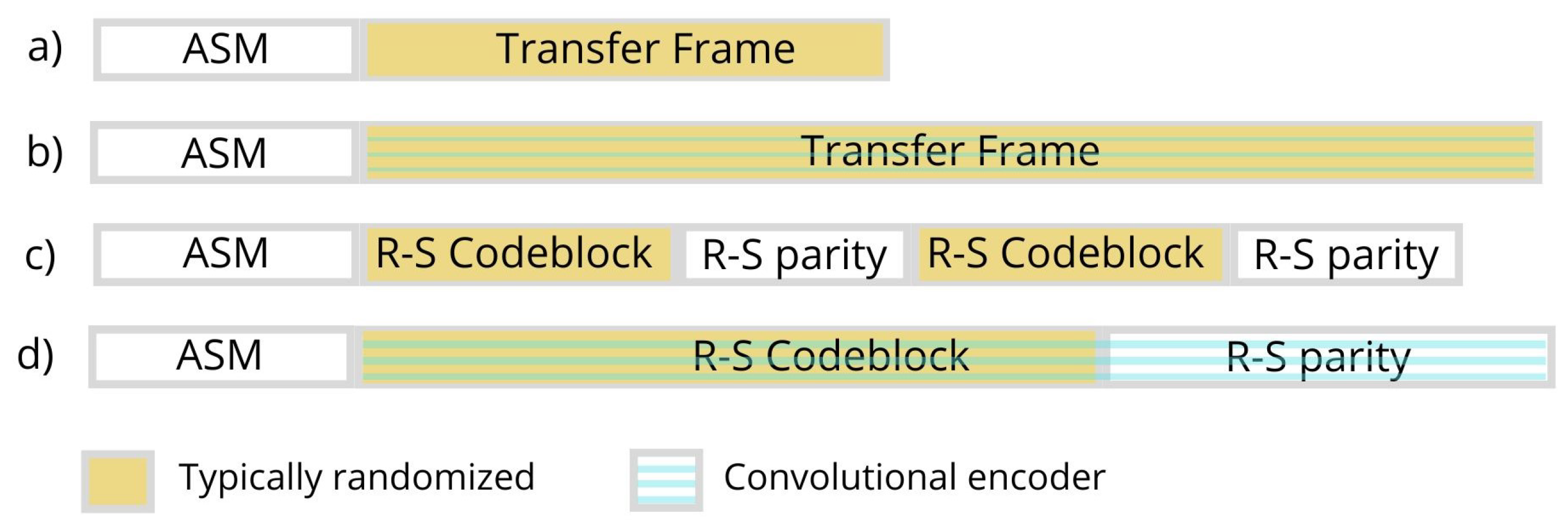
The ASM plays a fundamental role in the telemetry channel-processing chain by enabling the receiver to reliably synchronize frames or channel code blocks. According to [
3,
30], this is achieved by inserting a fixed synchronization marker before each channel code block, thereby forming the Channel Access Data Unit (CADU).
For telemetry data that is not turbo-coded, the ASM consists of a 32-bit (4-octet) synchronization pattern with the hexadecimal value 0x1ACFFC1D.
The marker must be inserted immediately before each code block, without any intervening bits. In this implementation, the ASM is appended directly to the encoder output and transmitted without additional encoding. This preserves the original synchronization pattern and facilitates reliable detection at the receiver using correlation techniques.
The block performs three main functions:
The block determines the end of each code block by monitoring the value of last signal. Once the end of the block is detected, the internal control logic is reset to ensure that the subsequent block also begins with the insertion of the ASM.
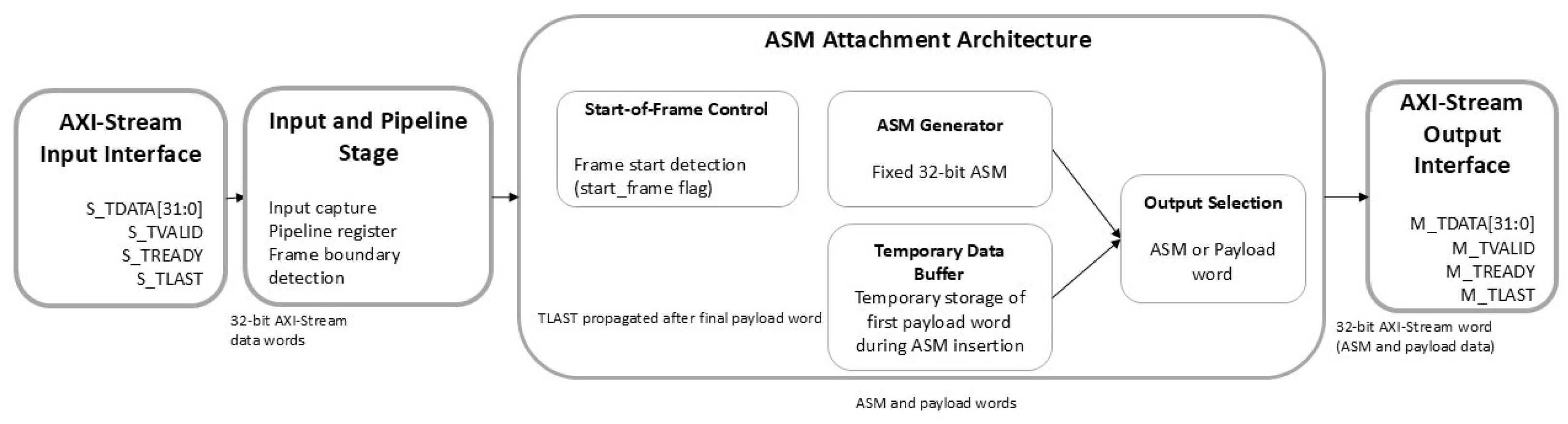
At the start of each code block, the module inserts the fixed ASM constant before transmitting the encoded payload. To achieve this, the first payload word is temporarily stored while the ASM is transmitted. During the following clock cycle, the stored payload word is released and normal data streaming resumes.
Figure 14 shows the hardware architecture of the ASM attachment block, helping to clarify how the framing stage works. The design inserts a synchronization marker at the start of each code block and maintains continuous AXI4-Stream data flow.
Figure 14 shows that the ASM attachment block has an input and pipeline stage, a start-of-frame control unit, an ASM generator, and an output selection stage. The start-of-frame control logic finds the start of each code block and then inserts the synchronization marker. The ASM generator supplies a fixed 32-bit synchronization word. A temporary buffer keeps the inserted ASM and the payload data properly aligned. The output selection stage sends either the ASM or the payload words, ensuring the AXI4-Stream data flow remains continuous.
The payload data remain unchanged, and the ASM is inserted only once per code block. The implementation guarantees the following properties:
A fixed 32-bit synchronization pattern.
Deterministic placement immediately before each code block.
No additional fill bits preceding the ASM.
Preservation of payload integrity.
Compatibility with standard correlator-based ASM detection.
The marker is inserted directly at the encoder output and transmitted without additional encoding. This approach satisfies the synchronization requirements specified in [
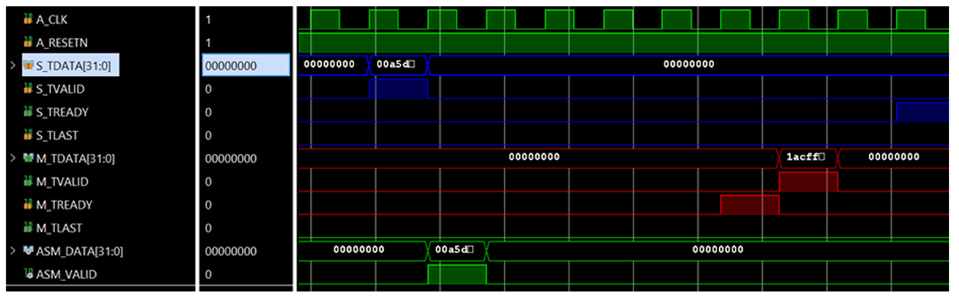
3] for non-turbo-coded telemetry channels while maintaining a simple architecture and predictable timing behavior. The correct operation of the ASM attachment block is validated through simulation, as shown in
Figure 15.
3.7. Pseudo-Randomizer
Reliable bit or symbol synchronization in telemetry systems requires a sufficient number of signal transitions. Highly structured data patterns, such as long sequences of identical bits, can hinder signal acquisition and clock recovery at the receiver. To mitigate this issue, the standards [
3,
30] recommend applying pseudo-randomization to the encoded telemetry stream.
According to [
3], the pseudo-random sequence is generated using the polynomial
This polynomial defines an eight-stage Linear Feedback Shift Register (LFSR) that generates a maximal-length sequence with a period of 255 bits. As specified by the standard, the register is initialized to the all-ones state at the beginning of each transfer frame. The randomized output is obtained by performing a bitwise modulo-2 addition between the input data sequence
and the pseudo-random sequence
This process is reversible and improves the statistical and spectral properties of the transmitted signal.
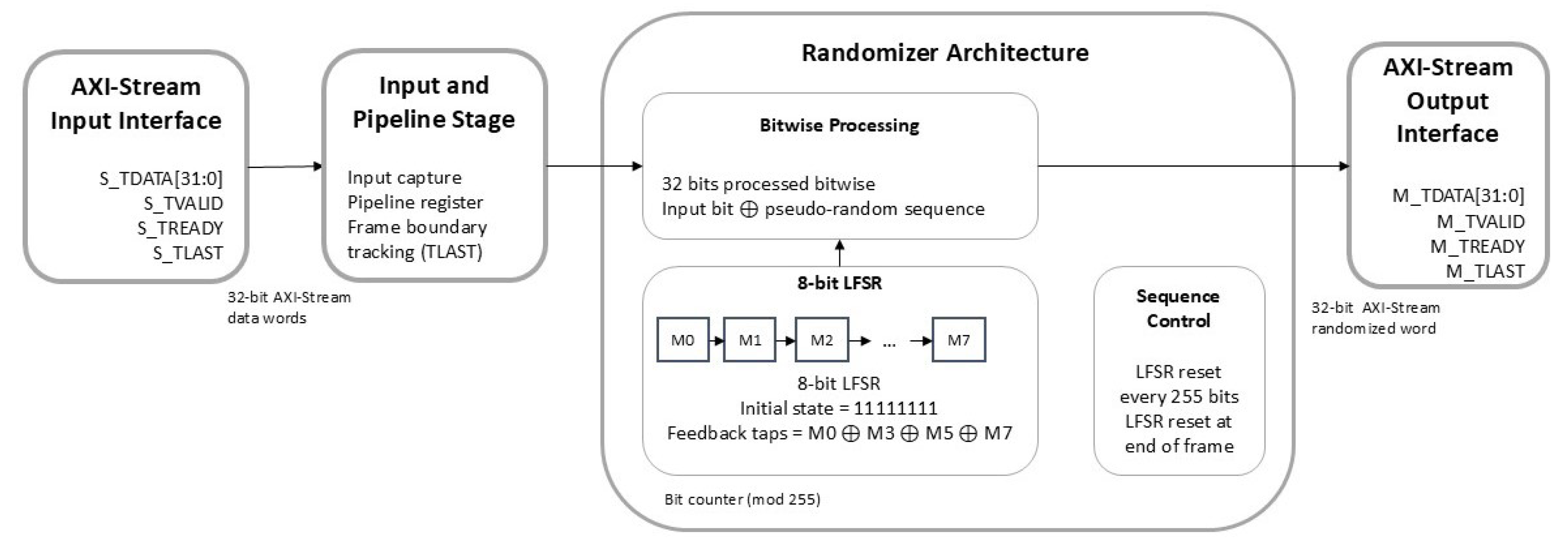
The design implements the standard LFSR structure defined by the specified polynomial. The feedback is derived from the corresponding tap positions, and the register is updated at each clock cycle. Scrambling is performed at the bit level, allowing the pseudo-random sequence to continue seamlessly across word boundaries. To provide a clear view of the hardware implementation,
Figure 16 presents the architecture of the proposed randomizer block.
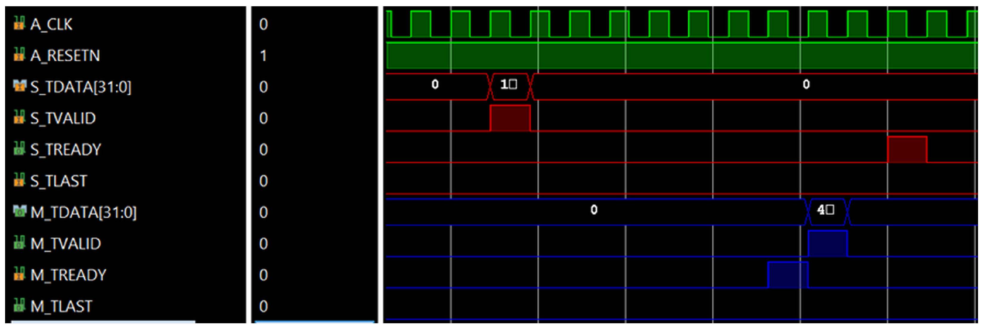
Figure 16 shows that the randomizer architecture includes an input and pipeline stage, a bitwise processing unit, an 8-bit LFSR, and a sequence control block. The bitwise processing unit adds the input data and the pseudo-random sequence from the LFSR using modulo-2 addition. The sequence control logic handles LFSR initialization and periodic resets. It ensures the system follows the specified polynomial and remains synchronized across transmitted frames. This setup enables continuous AXI4-Stream operation and maintains the statistical properties required for reliable telemetry transmission. To validate the correct operation of the implemented randomizer, simulation results are presented in
Figure 17.
3.8. BPSK Modulator
BPSK is a digital modulation technique that sends information by switching the carrier phase between two opposite values, usually 0° and 180°. This approach is widely used in space telemetry because it performs well in noisy channels and is the standard reference for comparing coding performance across many industry standards.
The BPSK modulator was built in VHDL as a symbol mapper using a straightforward 2:1 selection method. The digital carrier waveform is created outside the modulator or supplied by a BPSK, and comes in two forms, namely, In-phase carrier (0° phase) and Inverted carrier (180° phase shift).
From the transmitter’s point of view, the BPSK modulator always works as a binary phase mapper (0° or 180°). The difference between soft and hard operation comes from how the receiver makes decisions and how the decoder uses them. To clarify the internal implementation of the modulation stage,
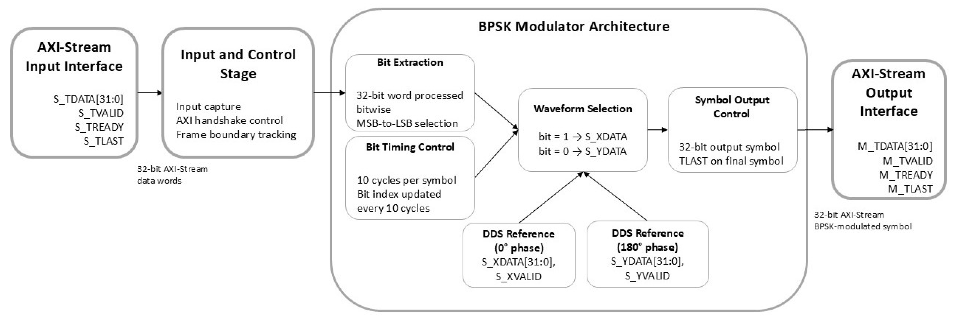
Figure 18 presents the hardware architecture of the BPSK modulator. The design processes each 32-bit AXI4-Stream input word bit by bit and selects one of two externally generated reference waveforms according to the input bit value.
Figure 18 shows that the BPSK modulator has an input and control stage, a bit extraction unit, a timing control block, a waveform selection stage, and an output control unit. The modulator processes each input word one at a time, starting with the most significant bit and extracting one bit at each step. For each bit, the modulator selects one of two externally provided reference waveforms, each representing a BPSK phase state. The chosen waveform remains active for a fixed number of clock cycles to maintain consistent symbol duration. The output control logic handles AXI4-Stream signaling and sends the TLAST signal at the end of each frame.
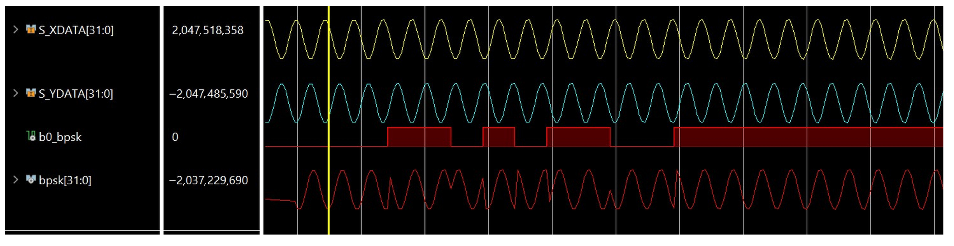
To validate the correct operation of the BPSK modulator, simulation results are presented in
Figure 19.
Figure 19 illustrates the behavior of the BPSK modulator under AXI4-Stream operation. The results show that, for each input bit, the modulator correctly selects one of the two reference waveforms corresponding to the two phase states. The continuity of the output waveform and the correct synchronization with the AXI4-Stream control signals. These results confirm the correct functionality of the implemented modulation scheme.
In digital communication systems, the decoding strategy adopted at the receiver plays a critical role in determining the overall error-correction performance of the channel coding scheme. Two principal approaches are commonly employed: hard-decision decoding and soft-decision decoding. These techniques differ primarily in how the received signal is quantized and how much reliability information about each symbol is preserved for the decoding process.
Hard-decision decoding operates on binary decisions obtained directly from the demodulator. The receiver first maps each received sample to the closest constellation point and converts it into a discrete symbol or bit, typically represented as either 0 or 1. This process effectively discards the amplitude or confidence information contained in the received signal, retaining only the final binary estimate. The decoder then processes this binary sequence using the selected error-correcting code algorithm, such as algebraic decoding for block codes or the Viterbi algorithm for convolutional codes. The principal advantage of hard-decision decoding is its simplicity: it requires less computational complexity, less memory, and simpler hardware implementation. For this reason, it has historically been used in systems with strict power or hardware constraints, as well as in legacy communication standards.
In contrast, soft-decision decoding preserves the reliability information associated with each received symbol. Instead of reducing the demodulator output to a binary value, the receiver provides the decoder with a quantized or continuous reliability metric, often expressed as a likelihood value or a log-likelihood ratio (LLR). These metrics indicate the probability that a received bit corresponds to a logical “0” or “1”. By exploiting this additional information, the decoder can weigh competing hypotheses more effectively when correcting errors. For example, in convolutional coding, the soft-input version of the Viterbi algorithm evaluates path metrics using Euclidean or log-likelihood distances rather than simple Hamming distances. This richer information significantly improves the decoder’s ability to distinguish between noise-induced errors and genuine signal transitions.
The performance difference between the two approaches is well established in information theory and practical communication systems. Soft-decision decoding typically provides a coding gain of approximately 2 dB compared to hard-decision decoding for many channel coding schemes, including convolutional codes and modern iterative codes. This improvement arises because the decoder retains partial information about the reliability of each received symbol rather than discarding it during the initial decision stage. Consequently, soft-decision decoding is particularly beneficial in channels dominated by additive noise, such as those modeled by AWGN, where the received signal amplitudes naturally contain reliability information.
Despite its superior error-correction performance, soft-decision decoding requires higher computational resources and larger memory bandwidth. The decoder must process multi-bit reliability metrics instead of simple binary symbols, which increases arithmetic complexity and data throughput requirements. As a result, system designers must carefully balance performance and implementation cost when selecting a decoding strategy.
In practical applications, the choice between hard and soft decoding depends on the system requirements and the type of channel coding employed. Hard-decision decoding remains common in systems where simplicity, low power consumption, or deterministic latency are critical, and it is often used with algebraic block codes such as Reed–Solomon codes. Conversely, soft-decision decoding is widely adopted in high-performance communication systems, including deep-space communications, modern satellite telemetry, and advanced wireless standards. These systems rely on the additional coding gain provided by soft reliability information to approach the theoretical limits of channel capacity and to maintain reliable communication under severe channel conditions.
In this paper, the two decoding schemes have been implemented and optimized for lowering the energy consumption and the processing time.
Because several processing blocks, such as the interleaver, randomizer, and BPSK modulator, are standardized, this work does not describe their internal structures in detail. These components follow CCSDS/ECSS specifications and are well documented in the literature. As a result, this paper mainly focuses on the system-level FPGA architecture and how it is efficiently integrated, while still giving enough design details for reproducibility.
4. The Measurement-Based Analysis and Experimental Results
To experimentally validate the transmitted waveform generated by the implemented architecture, deterministic test patterns were used as input to the system. The output signal was observed using real measurements and laboratory equipment.
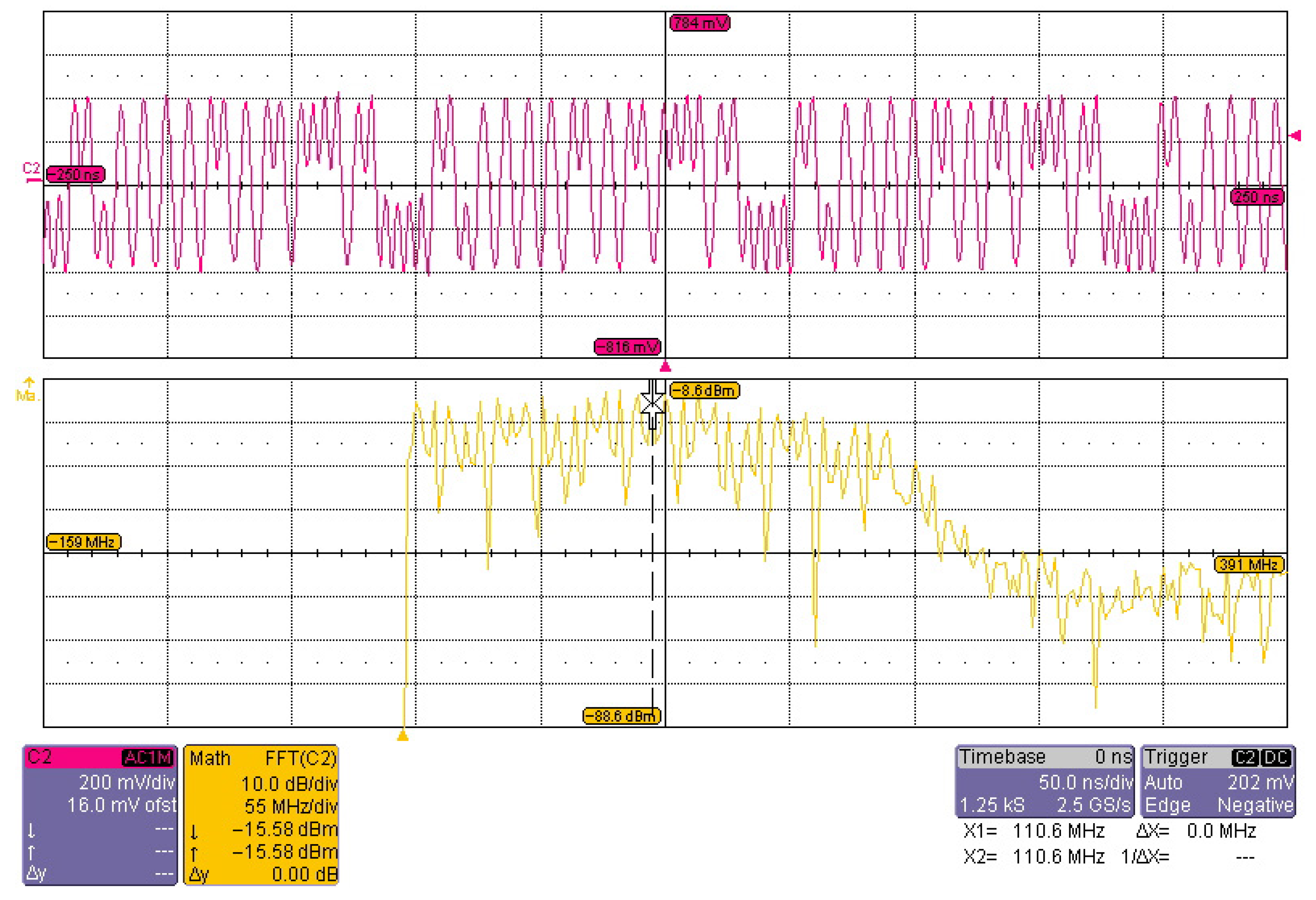
Figure 20 shows the waveform measured in both time and frequency domains using a digital oscilloscope.
In addition to the measurement-based analysis,
Table 1 summarizes the experimental validation method. The evaluation used a real-time hardware setup of the full transmission chain, which included channel coding, interleaving, randomization, and BPSK modulation. Deterministic test patterns served as input data to make the results repeatable and help verify how the system behaves.
Table 1 shows that the validation checks signal integrity, timing behavior, and whether the whole transmission chain works correctly.
Figure 20 shows the measured BPSK signal from the system, allowing us to observe the transmitted waveform in both the time and frequency domains.
The upper trace illustrates the transmitted BPSK signal in the time domain, where phase transitions corresponding to the encoded binary symbols are evident. These phase inversions constitute the modulation mechanism that maps binary data onto the carrier waveform.
The lower trace shows the frequency spectrum of the same signal obtained via Fast Fourier transform (FFT) analysis. The measured spectral distribution demonstrates the expected energy concentration around the carrier frequency, consistent with the theoretical behavior of BPSK modulation.
The proposed architecture was synthesized and implemented in the target FPGA using Vivado design tools. Post-implementation reports evaluated hardware resource utilization and performance margins. In addition to external measurements, internal signals were monitored during implementation to verify correct operation of each processing stage and ensure proper synchronization across the transmission chain.
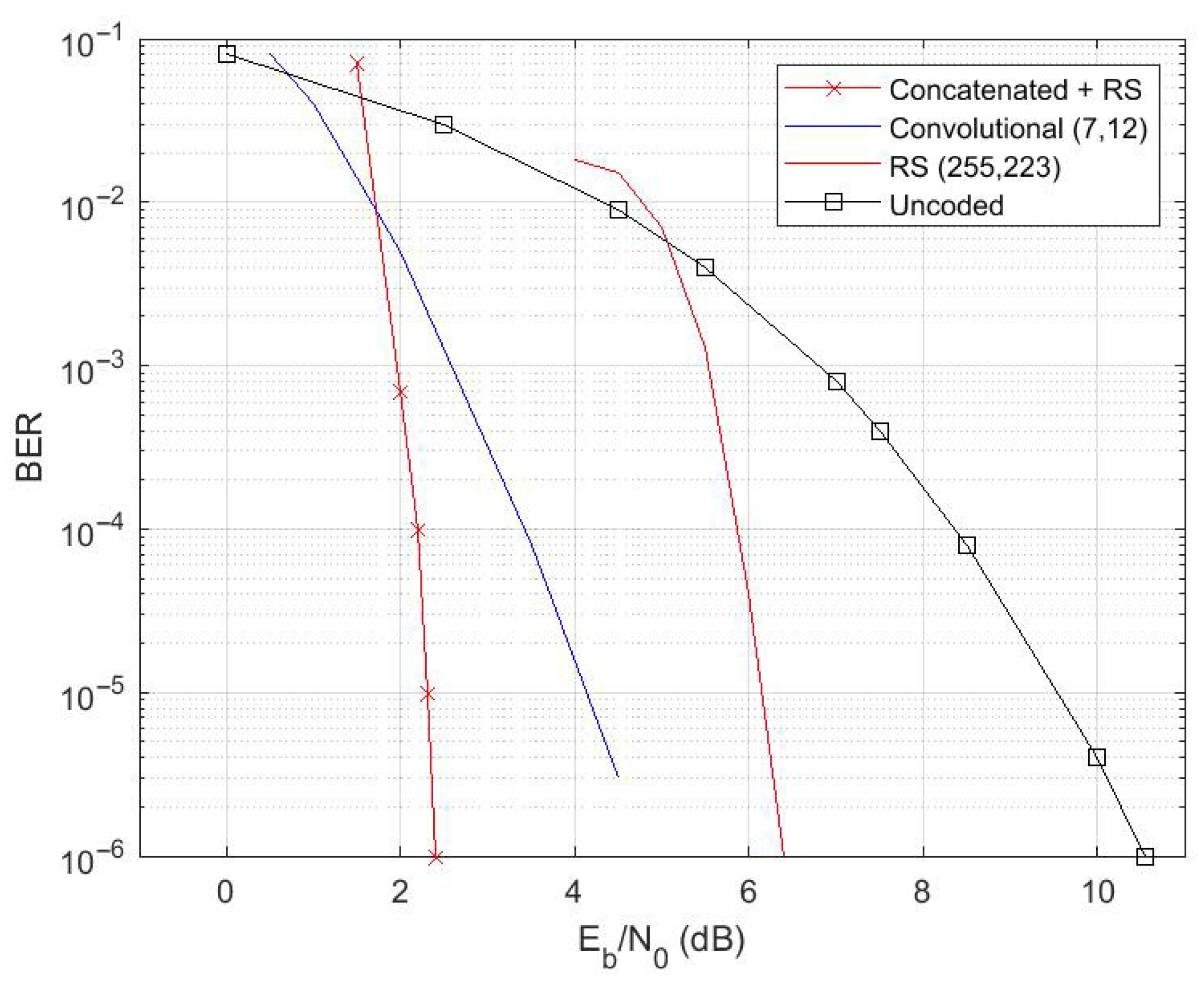
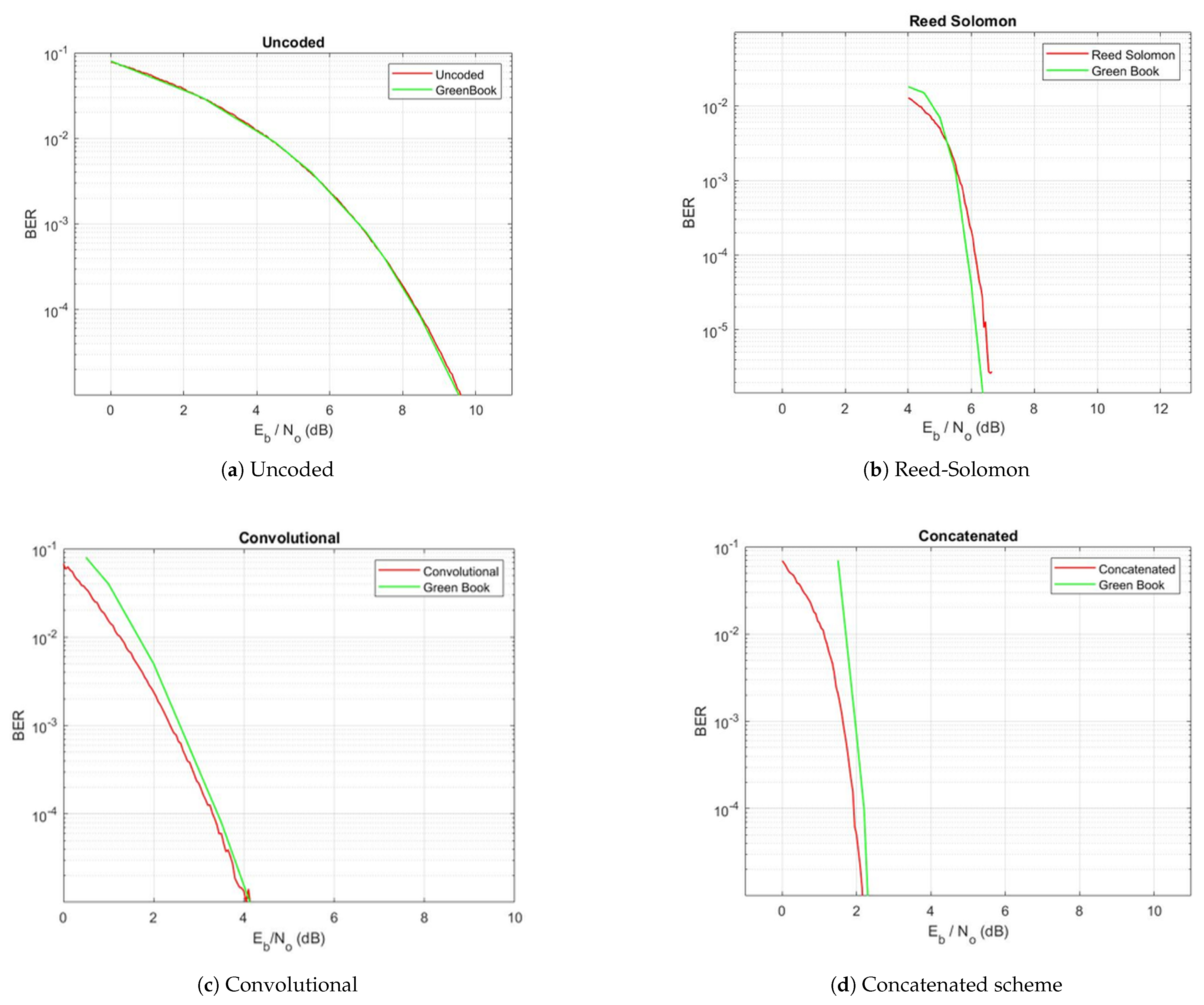
Figure 21 shows how BER changes with
for four setups: uncoded transmission, convolutional coding, Reed–Solomon coding, and the concatenated coding scheme. In every case, the system’s results are very close to the theoretical curves from the CCSDS Green Book. In the uncoded case, the BER curve matches the expected results for BPSK modulation over an AWGN channel. This confirms that the modulation and demodulation stages work correctly. With convolutional coding, there is a clear coding gain, as the BER curve shifts to lower
values. The results from the system closely follow the theoretical reference, showing that the convolutional encoder and decoder are working as intended. Similarly, Reed–Solomon coding shows improved error-correction performance, particularly at moderate signal-to-noise ratios. The alignment between the simulated results and the reference model confirms the correct behavior of the block coding stage. These BER results help confirm how well the coding schemes work under channel conditions. They do not directly measure the system’s maximum possible throughput, which comes from the architecture and is checked through timing analysis.
The concatenated scheme, combining Reed–Solomon and convolutional coding, achieves the best overall performance. A significant coding gain is observed, with a steep reduction in BER at relatively low values. This behavior is consistent with the theoretical expectations for concatenated forward error-correction schemes and validates the correct integration of both coding stages. Overall, the close match between the system’s results and the CCSDS 130.1-G-1 reference curves shows that the whole transmission chain, encoding, interleaving, modulation, and data handling, works as intended.
These results come from controlled simulations that used an AWGN channel and assumed perfect synchronization at the receiver. These conditions help focus on the effects of the coding schemes and check their performance against the theoretical CCSDS 130.1-G-1 reference [
30].
A comparison summary of the supported coding modes is presented in
Table 2. The proposed architecture enables four different configurations: uncoded transmission, convolutional coding, R-S coding, and concatenated coding. The system uses a 32-bit AXI4-Stream interface running at 110 MHz, which gives a raw data rate of 3.52 Gbps for each mode. As a result, the uncoded mode reaches the full transmission rate. The coded modes have lower rates, depending on their code rates. In particular, the implemented R-S encoder follows an
configuration, resulting in an effective code rate of
, and an achievable throughput of
. For the concatenated scheme combining
and a rate
convolutional encoder, the resulting effective code rate is
, corresponding to a net throughput of
.
In addition, the coding gain values included in
Table 2 are estimated based on well-established CCSDS/ECSS performance curves reported in the literature. These values provide a representative indication of the error-correction capability of each scheme without requiring extensive bit error rate simulations, which are outside the scope of this work. All coding modules are already set up in the FPGA fabric, so you can choose the coding scheme you want without needing to reconfigure or re-synthesize the system. Unlike traditional methods that test coding techniques separately, this system uses a single, flexible design that can adjust to different communication needs as they happen. This comparison further demonstrates that the main contribution of the proposed design is not only the implementation of individual coding schemes, but the integration of all supported modes within a single FPGA-based architecture, enabling real-time adaptability with minimal overhead.
The selected configuration represents a practical trade-off between redundancy and throughput, prioritizing high data rates while still providing burst-error-correction capability, which is particularly suitable for high-throughput telemetry applications.
Table 3 summarizes the hardware utilization after place-and-route.
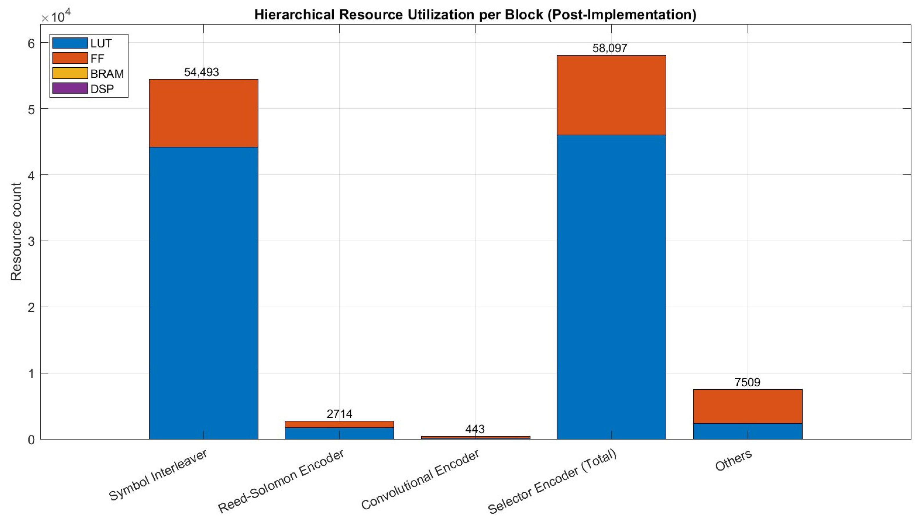
To better understand the architecture’s complexity, we broke down the resources by hierarchy. While
Table 3 and
Figure 22 provide a quantitative overview of FPGA resource utilization, a deeper analysis can identify the main architectural bottlenecks and design trade-offs.
Figure 22 shows that the Symbol Interleaver uses the most LUTs and flip-flops. This result is expected, as interleaving involves significant data reordering and indexing, especially with the large interleaver depth used. These tasks need a lot of combinational logic, making this block the most resource-heavy part of the design.
In contrast, the Reed–Solomon and convolutional encoder blocks exhibit a considerably lower hardware footprint. Their internal operations are more structured and rely on well-defined arithmetic and shift-register-based processes, which result in a more efficient hardware implementation.
Furthermore, the consistently low utilization of BRAM and DSP resources across all processing stages indicates that the proposed architecture depends primarily on logic rather than memory or computation. As a result, the architecture is more scalable, allowing for the integration of additional features such as advanced error detection, adaptive coding, or deeper interleaving without significantly increasing overall resource consumption.
Figure 22 shows that hardware resources are not evenly spread across the processing stages. The interleaving block uses most of the logic. This figure makes it easier to spot where to focus optimization and shows how each coding part affects the total hardware cost. A complete description is shown in
Table 4.
This breakdown shows that most of the design complexity is in the interleaving stage. The other blocks have a much smaller effect on total resource use. Because of this modular setup, it will be easier to optimize and scale the system in the future.
This study also looked at other ways to implement interleavers, such as using memory-based architectures with BRAM and pipelined designs. BRAM-based methods can lower LUT use, but they add memory access delays and need more complicated address control. Pipelined designs can help with timing, but they make the design more complex and use more resources.
Therefore, a logic-based implementation was chosen because it offers high throughput, predictable performance, and is easy to integrate into the data path. Although deeper pipelining or additional buffering could further reduce the combinational path depth and increase the maximum operating frequency, the implemented architecture already meets the timing requirements of the complete system and achieves stable operation at the target clock frequency.
The design was set to run at a clock frequency of 110 MHz. After routing, timing analysis showed that all user-defined timing constraints were met.
The timing summary reports:
The positive setup slack means the design meets the required clock period with a good timing margin. While the hold slack is small, it is still positive, so there are no hold violations.
Using the setup slack, we can estimate the maximum operating frequency as follows:
Effective minimum achievable period:
Estimated maximum frequency:
So, the architecture could theoretically run at about 129 MHz under these conditions. This margin shows the design is timing-safe at the target frequency and has some room for scaling. The proposed architecture is capable of achieving up to 1.76 Gbps under fully parallel operation. This value is derived from the system clock frequency and the 32-bit data path implemented across the FPGA transmission chain. This throughput corresponds to the sustained processing capability of the architecture under continuous data streaming conditions and is supported by the successful timing closure at the target clock frequency. The system operates at a clock frequency of 110 MHz and processes 32 bits per clock cycle, resulting in a raw data throughput of 3.52 Gbps. When the convolutional encoder is enabled, its coding rate of 1/2 doubles the number of transmitted bits, yielding an effective information throughput of up to 1.76 Gbps. A summary of the parameters used in this calculation is provided in
Table 5. As a result, the effective information throughput is:
It is important to note that the reported throughput corresponds to the effective processing rate achieved under continuous, fully parallel streaming operation. The actual net user data rate is determined by the selected transmission mode, the chosen coding scheme, and frame-level overheads, including synchronization markers and, when activated, Reed–Solomon redundancy.
Power consumption figures were obtained from the post-implementation netlist using switching activity data extracted from functional simulation. The activity information was exported in SAIF and imported into the Vivado Power Analyzer. This SAIF-based methodology provides significantly higher accuracy compared to vector-less (probabilistic) estimation techniques.
The proposed architecture consumes approximately 1.77 W of total on-chip power in the uncoded, convolutional, and Reed–Solomon modes. Of this, dynamic power accounts for roughly 0.68 W and static (leakage) power for 1.09 W. Power consumption remains nearly identical across these three configurations because the design keeps all processing blocks in the programmable logic permanently active. The different coding schemes are implemented through multiplexing rather than power gating, resulting in comparable switching activity levels in all cases.
In contrast, the concatenated (convolutional + Reed–Solomon) mode exhibits higher power consumption, with total on-chip power rising to 1.916 W and dynamic power to 0.824 W—representing an increase of approximately 21% in dynamic power relative to the uncoded configuration. This increase is primarily driven by higher signal and logic activity: signal power rises from 0.208 W to 0.315 W, while logic power increases from 0.255 W to 0.304 W. Contributions from BRAM, DSP blocks, and clock management resources remain largely unchanged and do not significantly affect the overall difference.
These results demonstrate that the proposed architecture maintains a nearly constant energy profile across different coding schemes, with the concatenated configuration representing the worst-case power scenario.
Table 6 presents the total, dynamic, and static power consumption for the different coding modes supported by the system.
A detailed breakdown of the dynamic power is presented in
Table 7.
These results demonstrate that the architecture maintains a nearly constant energy profile across the majority of coding configurations, with the concatenated mode representing the worst-case power scenario. Although the Vivado Power Analyzer reports a medium confidence level, the use of simulation-derived SAIF data substantially enhances the reliability of the estimates. Overall, the design exhibits predictable and scalable power behavior, which is highly advantageous for satellite communication systems subject to stringent power and thermal constraints.
5. Conclusions
This work presents the complete FPGA-based design, implementation, and verification of a concatenated channel coding architecture integrating Reed–Solomon encoding, convolutional encoding, symbol interleaving, and pseudo-randomization. The proposed system targets high-reliability digital communication scenarios where deterministic timing, robustness against channel impairments, and efficient hardware utilization are critical requirements. By integrating these complementary coding and signal conditioning techniques into a single hardware architecture, the design demonstrates the practical feasibility of implementing a standards-compliant forward error-correction chain within a compact and scalable FPGA solution.
Post-implementation timing analysis confirms reliable operation at the target clock frequency of 110 MHz with positive setup and hold margins across the design. The measured setup slack provides additional timing headroom, yielding an estimated maximum operating frequency of approximately 130 MHz. These results validate the architectural choices adopted during the design process, particularly the pipeline structure and balanced combinational paths, and demonstrate that stable high-frequency operation can be achieved without relying on aggressive placement constraints or extensive timing optimization techniques.
From a hardware perspective, the implementation exhibits efficient resource utilization relative to the available FPGA capacity. The symbol interleaving stage represents the most resource-demanding component, primarily due to the bit-reordering and frame-structuring operations required to achieve effective burst-error mitigation. In contrast, the Reed–Solomon and convolutional encoders present comparatively modest logic requirements, reflecting the efficiency of their hardware-oriented implementations. Furthermore, the minimal use of BRAM and DSP resources indicates that the architecture is predominantly logic-based and highly modular, which simplifies integration with other signal-processing subsystems.
Analysis of power consumption using SAIF-annotated switching activity reveals a total on-chip power of approximately 1.77 W for the uncoded, convolutional, and R-S modes. This value increases moderately to 1.916 W in the concatenated configuration. The results demonstrate that the architecture maintains a nearly constant energy profile across various coding schemes. The concatenated mode represents the worst-case operating condition because of increased processing activity. These findings confirm the suitability of the proposed design for deployment in energy-constrained embedded and satellite communication systems. Furthermore, the consistent power behavior across configurations highlights the efficiency of the fully integrated architecture without requiring power-gating techniques.
When considering timing performance, resource utilization, and power consumption collectively, the results highlight several key achievements of the proposed architecture:
Deterministic and timing-safe operation at the target system frequency.
Efficient logic utilization with minimal dependence on dedicated FPGA resources.
A modular and scalable architecture suitable for integration into larger communication systems.
Power characteristics compatible with embedded high-reliability communication platforms.
The main contribution of this work lies in the hardware architecture and implementation methodology, rather than in adopting a specific standard version. While the reference implementation uses a classical telemetry coding scheme, these techniques remain relevant across various space communication contexts, notably in systems that require deterministic performance, reduced complexity, and efficient use of hardware resources.
Current standards are built on the foundations established by earlier telemetry coding schemes, extending their functionality while continuing essential structural principles. Within this system, the proposed design remains applicable to both existing and legacy systems and provides a robust, reusable baseline for the development of future telemetry architectures, including those that conform to more recent CCSDS-based standards.
Overall, the implementation demonstrates that classical concatenated forward error-correction schemes can be efficiently realized on modern FPGA platforms while maintaining high performance, architectural clarity, and implementation flexibility. These results reinforce the continued relevance of concatenated coding architectures in contemporary digital communication systems, particularly in applications requiring predictable hardware behavior and robust error-correction capabilities.
While the results are promising, there are some limitations to this work. The implementation only covers the transmitter side of the communication chain, so a full end-to-end system with the receiver is not included. Also, we have not tested performance under realistic channel conditions, such as BER or Frame Error Rate (FER), because our main goal was to focus on hardware architecture design and real-time implementation.
In future work, we plan to extend the proposed system into a complete communication link by adding a receiver chain and channel models. This will let us evaluate performance more fully under real-world conditions. We will also look into using more advanced coding schemes that meet the latest CCSDS standards. This approach will let us directly compare theoretical performance with practical results, which will help confirm the value of the proposed architecture.