Article

A Device-Centric Research of Power Side-Channel in FPGAs
School of Electronics and Information Technology (School of Microelectronics), Sun Yat-sen University, Guangzhou 510006, China
*
Author to whom correspondence should be addressed.
Electronics 2026, 15(8), 1546; https://doi.org/10.3390/electronics15081546
Submission received: 4 March 2026 / Revised: 5 April 2026 / Accepted: 6 April 2026 / Published: 8 April 2026
(This article belongs to the Special Issue Secure and Privacy-Enhanced Data Sharing)

Abstract

As a widely used computing substrate, the side-channel security of FPGAs has attracted considerable attention, yet a systematic understanding of how FPGA device types contribute to exploitable leakage remains limited. This work presents a device-centric evaluation that maps an S-box-like function onto common FPGA primitives, including look-up table (LUT), flip-flop (FF), block RAM (BRAM), and distributed RAM (LUTRAM), and assesses Correlation Power Analysis (CPA) outcomes under the Hamming Weight (HW) and Hamming Distance (HD) power models. The results show pronounced leakage differences across device types: FF- and BRAM-based implementations exhibit substantially stronger leakage than LUT- and LUTRAM-based ones, and they frequently achieve GE = 0 in our configurations, while the HD model is generally more effective than the HW model in the performed CPA evaluations. Notably, FF-, BRAM-, and LUTRAM-based implementations can already be breakable starting from one instance under the HD model in our device-level tests, indicating that exploitable leakage may manifest in real FPGA applications. These device-level observations are further validated on a practical cipher by analyzing two SM4 encryption modules that differ only in the S-box implementation style; the BRAM-based design shows significantly stronger leakage than the LUT-based design, achieving GE = 2.58 versus GE = 78.3 at 10,000 traces. This work highlights the critical role of device selection and implementation style in FPGA side-channel security, and it provides practical insights for designing secure FPGA applications against power side-channel analysis.

1. Introduction

With the rapid advancement of cloud computing and heterogeneous computing, Field-Programmable Gate Arrays (FPGAs) have become an important hardware platform for cloud acceleration and embedded encryption computing due to their high parallelism and reconfigurability [1,2]. The flexible logic reconfiguration of FPGAs improves resource utilization while bringing severe hardware security threats, among which power side-channel attacks have become a research focus in FPGA security for their strong concealment and low implementation threshold [3]. As a method to apply side-channel attacks, power analysis was first proposed by Kocher in 1999 [4]. The more powerful Correlation Power Analysis (CPA) method was proposed in 2004 [5]. Most side-channel studies take cryptographic algorithms as their primary research targets, and FPGA implementations of block ciphers represent a typical class of security-critical applications. Among them, the Advanced Encryption Standard (AES) and the Chinese national standard SM4 are representative examples. AES has been widely adopted in mainstream security protocols and products, whereas SM4 is extensively used in China compliance-oriented systems. Typically, both ciphers operate on 128-bit data blocks, and their encryption rounds follow an iterative structure based on substitution and shifting/permutation operations, which leads to substantial similarities in their FPGA implementations.
Previous research on FPGA power side-channels has yielded achievements in two dimensions. In terms of practical attacks on cryptographic implementations, prior work has demonstrated that ring-oscillator (RO) sensor networks can be used to monitor on-chip power variations and enable simple power analysis (SPA) against RSA modules, recovering private keys even under physical isolation [6]. It has also been shown that carry-chain-based time-to-digital-converter (TDC) voltage sensors support Correlation Power Analysis (CPA) key extraction for AES without direct signal connections, and the attack remains effective even when the sensor is placed far from the target logic [7]. These techniques have further been adapted to cloud FPGA platforms, where CPA extraction of AES-128 keys was demonstrated on the Amazon EC2 F1 architecture, confirming side-channel vulnerability in multi-tenant environments [8]. Beyond on-chip voltage sensing, a recent work introduced a new attack surface by leveraging widely integrated current sensors in ARM-FPGA SoCs, showing that current measurements can be highly sensitive to FPGA activity and enable effective inference of workload and key-related properties [9]. In addition, instruction-level leakage has also been investigated for FPGA-based computing substrates: a work using on-chip TDC sensing demonstrated that opcode classification on soft-core CPUs remains feasible under practical isolation constraints, highlighting that even small compute blocks can contribute observable leakage [10]. Similarly, another work showed that power traces acquired via on-chip sensing can reveal instruction types and layer-level characteristics of neural-network accelerators, posing risks to both runtime confidentiality and model IP [11]. In terms of hardware leakage mechanisms, studies have identified new vulnerability types across multiple Xilinx FPGA families and clarified that leakage intensity can vary with routing and device structures [12]. In addition, it has been validated that malicious tenants can trigger chip-wide voltage fluctuations via power-waster circuits on Intel FPGAs, enabling cross-region fault injection and RSA key theft [13].
However, existing research still lacks a systematic investigation of how cryptographic implementations on different device types contribute to power side-channel leakage. Most prior analyses focus on what information can be inferred from concrete targets such as specific cryptographic algorithms or instructions running on soft-core, rather than on where the exploitable leakage carriers originate from within the FPGA fabric. Although a study [12] has investigated leakage mechanisms from a more principle-oriented perspective, its emphasis is placed on routing effects and leakage behaviors at the level of a limited set of configurable logic blocks, instead of the more frequently used fundamental primitives that FPGA designs are ultimately mapped onto. Given that diverse real-world applications on FPGAs are mainly realized by mapping computations and storage onto such basic resources, a device-centric understanding is essential for identifying the leakage carriers and enabling more targeted protection strategies.
To address this gap, we conduct a comprehensive study of multiple circuit implementations on FPGA fabric, including block RAM (BRAM), flip-flop (FF), look-up table (LUT) and distributed RAM (LUTRAM), together with widely used power models. We characterize and compare the power side-channel leakage associated with different circuit implementations, and evaluate the attack performance achieved by various power models. And we introduce a case study on the SM4 block cipher, providing a validation that the conclusions drawn from the above device-centric analysis directly translate to practical security outcomes for deployed FPGA cryptographic applications. The selection of LUT, FF, BRAM, and LUTRAM is motivated by their representativeness in FPGA implementations of practical algorithms. LUTs and FFs constitute the most commonly used resources in FPGA designs: based on engineering experience, general arithmetic and logic operations (e.g., addition/subtraction, bit-wise operations, shifts, and small width multiplication/division) are typically mapped to LUT-based combinational logic, while the need for state retention and sequential circuit is primarily handled by FFs. For BRAM and LUTRAM, they are the fundamental on-chip memory resources on FPGAs. BRAM is typically used for larger memory requirements, while LUTRAM is often employed for smaller, more flexible memory needs. Together, these four primitives cover the dominant building blocks for computation and storage, enabling a device-level comparison that is directly relevant to real-world applications.
In this work, we show that BRAM, FF, and LUTRAM exhibit potential susceptibility to power side-channel leakage in some configurations, with BRAM and FF presenting markedly stronger leakage, whereas LUT does not show exploitable leakage in our evaluation. In addition, we find that the HD model characterizes FPGA power consumption more accurately than the HW model. We further validate the former observations by comparing two SM4 modules that differ only in the implementation style of the attack point (LUT versus BRAM), where the BRAM-based design is significantly more vulnerable under CPA. This SM4 case study further suggests a practical countermeasure direction: selectively mapping algorithmic sensitive points to FPGA devices that are empirically harder to break, thereby reducing exploitable leakage by design.

2. Methods

Following common practice in this area, we adopt Correlation Power Analysis (CPA) as the primary analysis methodology in this work. Motivated by prior studies on block-cipher attacks and their selection of attack points (i.e., specific algorithmic intermediate variables), we note that the S-box output is consistently chosen as a representative leakage target. Accordingly, we design an S-box-like module as the core test primitive, which maps an 8-bit input to an 8-bit output. By instantiating this module on the FPGA using different device types, we are able to systematically evaluate and compare the power side-channel leakage characteristics associated with each resource. In addition, we analyze a complete SM4 encryption module to further validate the conclusions drawn from the above experiments.

2.1. Power Analysis Procedure

The Correlation Power Analysis exploits statistical correlation between predicted power consumption and actual measured power traces to recover secret information such as keys. For a given algorithm and known plaintext inputs, the key-dependent intermediate values can be derived, and the predicted power consumption can then be computed using Hamming Weight (HW) or Hamming Distance (HD) power models. Let x denote an n-bit intermediate variable during operation, and let HW ( · ) and HD ( · , · ) represent the HW and HD functions:
HW ( x ) = i = 0 n 1 x i ,
HD ( x , y ) = HW ( x y ) = i = 0 n 1 ( x i y i ) ,
where x i { 0 , 1 } is the i-th bit of x, y denotes the previous value of x, and ⊕ denotes bit-wise XOR. For example, let x = 11110000 and y = 00001111 , then HW ( x ) = 4 and HD ( x , y ) = HW ( x y ) = HW ( 11111111 ) = 8 .
During CPA, these predicted values are correlated with the measured traces to distinguish the correct key hypothesis from incorrect ones. We adopt the Pearson correlation coefficient between the predicted leakage vector { h i } i = 1 N and the measured samples { T i ( t ) } i = 1 N :
ρ k ( t ) = i = 1 N h i h ¯ T i ( t ) T ( t ) ¯ i = 1 N h i h ¯ 2 i = 1 N T i ( t ) T ( t ) ¯ 2 ,
where h ¯ and T ( t ) ¯ denote the sample means of { h i } and { T i ( t ) } , respectively [5].
The overall CPA procedure is summarized in Algorithm 1.
Algorithm 1: Correlation Power Analysis (CPA) procedure.
Electronics 15 01546 i001

2.2. Experimental Setup

We build our experimental platform on a Zedboard (Xilinx Zynq-7000, xc7z020clg484), which is logically divided into a power-consumption module and a power sensing module. Given that the distinctions between different Xilinx FPGA families (e.g., UltraScale) primarily lie in the quantity of basic resources rather than their architecture, we infer that our investigations on basic resources are also applicable to other Xilinx FPGA families. The power-consumption module comprises two components: (i) a device-level substitution unit based on the SM4 byte S-box S ( · ) , which is instantiated using different FPGA primitive types (LUT, FF, BRAM, and LUTRAM) to enable controlled leakage characterization, and (ii) a complete SM4 encryption module used as a case study to validate whether the device-level observations translate to a practical cipher implementation.

2.2.1. Power-Consumption Module: Device-Level Test Primitives

Following common practice in power side-channel analysis of block ciphers, where the S-box output is typically selected as the primary attack point, we design the power-consumption unit as an S-box-like function: an 8-bit input is transformed to an 8-bit output. Subsequently, to enable a device-level study of power side-channel leakage on commonly used FPGA resources, we explicitly constrained the implementation to map this unit onto specific FPGA primitives, including LUTs, FFs, BRAMs and LUTRAMs. Each mapped unit is referred to as an instance. For the detailed configuration, eight FFs are grouped into one instance, where the input is substituted through a lookup table and directly connected to the D of the flip-flop, and the expected value is output from the Q at the clock edge; for LUTs, each instance consists of eight LUT6 elements whose inputs are connected to the outputs of flip-flops that only register the input without performing substitution, thereby delivering the signals to the LUTs for substitution and output, while for BRAM and LUTRAM, the inputs serve as addresses to access the stored substituted values, each instance generates an 8-bit output, and the implementation style is explicitly specified to allow the synthesis tool to infer corresponding hardware resources automatically.
We vary the number of instances from one to the maximum feasible value to investigate the power side-channel characteristics of each device type as comprehensively as possible. All operations across different instances occur simultaneously. The floorplan region for all instances is explicitly constrained in the tool and placed around the power sensors, while their exact locations are automatically inferred by the tool without imposing constraints on contiguous placement. Table 1 shows detailed information about the experimental parameters. The actual device usage is verified by the implementation report, and the “Maximum number of devices” considers only the power-consumption unit and is limited by available resources. The power-consumption module operates at a 50 MHz clock frequency.
To emulate the repeated key-dependent substitutions that appear in practical block ciphers while keeping the logic footprint controllable, we drive the substitution function S ( · ) using 128-bit plaintext blocks. For each plaintext P { 0 , 1 } 128 , we partition it into 16 consecutive bytes, P = ( p 0 p 1 p 15 ) with p j { 0 , 1 } 8 . Starting from bits 0 to 7, one byte p j is broadcast to all instantiated substitution units per cycle. Since all instances receive the same input, they produce identical outputs in that cycle. Hence, each plaintext triggers 16 back-to-back evaluations of S ( · ) , which we refer to as 16 rounds. The 128-bit output formed by concatenating the 16 substitution results is stored for verification.

2.2.2. Power-Consumption Module: SM4 Encryption Implementation

To validate whether the device-level leakage observations translate to a practical cryptographic module, we further implement the SM4 block cipher as a case study on the same FPGA platform. In particular, we build two SM4 implementations that share the same architecture and the only difference is the implementation of the S-box, which is mapped either to BRAM or to LUT. This design ensures that any observed difference in CPA performance can be attributed to the underlying device type, thereby validating the conclusions drawn from the device-level experiments.
SM4 is a 128-bit block cipher with a 128-bit key and 32 rounds as shown in Algorithm 2. Let the plaintext be parsed into four 32-bit words ( X 0 , X 1 , X 2 , X 3 ) , where X i { 0 , 1 } 32 , and let RK r denote the 32-bit round key for round r { 0 , , 31 } . The round update is given by
X r + 4 = X r T X r + 1 X r + 2 X r + 3 RK r ,
where ⊕ denotes bit-wise XOR over 32-bit words and T ( · ) is the round transformation. The ciphertext is obtained by reversing the last four words:
( C 0 , C 1 , C 2 , C 3 ) = ( X 35 , X 34 , X 33 , X 32 ) .
The transformation T ( · ) is defined as a composition of a byte-wise substitution and a linear diffusion. Specifically, for a 32-bit word A = ( a 0 a 1 a 2 a 3 ) where a j { 0 , 1 } 8 are the four bytes and denotes concatenation, the nonlinear mapping is
B = τ ( A ) = ( S ( a 0 ) S ( a 1 ) S ( a 2 ) S ( a 3 ) ) ,
where S ( · ) is the SM4 8-bit S-box. The linear mapping is then applied to B:
T ( A ) = L τ ( A ) , L ( B ) = B ( B 2 ) ( B 10 ) ( B 18 ) ( B 24 ) ,
where n denotes a 32-bit left rotation by n bits.
Algorithm 2: SM4 encryption procedure.
Electronics 15 01546 i002

2.2.3. Power-Sensing Module and Platform Configuration

The power-sensing module is implemented as an on-chip TDC-based power sensor. Its operating principle relies on the fact that switching activity in the power-consumption module induces transient supply-voltage fluctuations (e.g., IR drop) on the shared power distribution network [14], which modulate the propagation delay of a dedicated delay chain. The TDC quantifies these delay variations and converts them into a digital code. In each acquisition, the resulting delay code sequence is used as the sample value T i ( t ) in the CPA workflow, serving as a proxy of instantaneous on-chip power consumption [15,16].
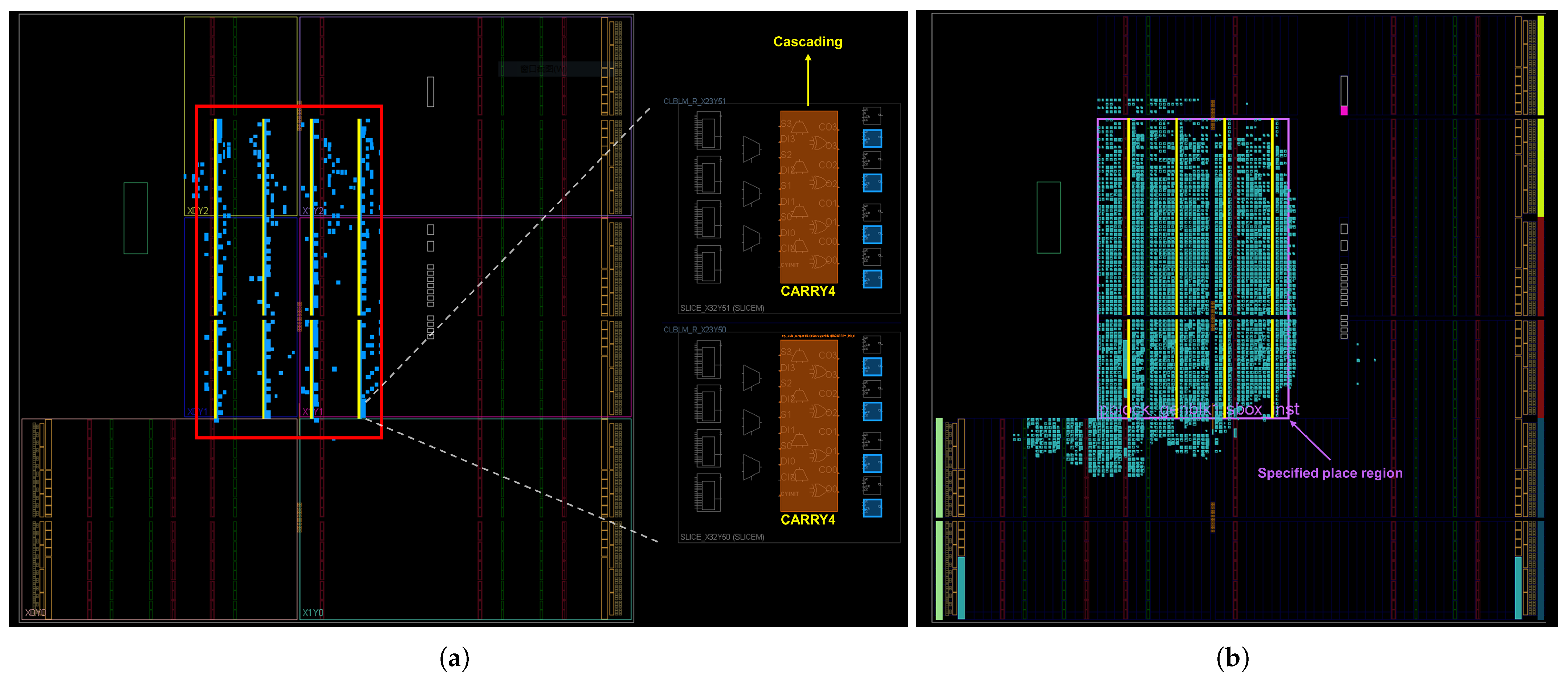
Following prior studies, we implement the TDC sensor by cascading CARRY4 adders to detect propagation delays along the carry chains. Four independent carry chains are adopted in our design, each consisting of 75 stages of CARRY4 units, yielding an effective carry length of 300 bits. We manually specify the position of the first-stage CARRY4 for each carry chain, and the synthesis tool automatically places the subsequent stages contiguously. As illustrated in Figure 1a, the four carry chains are enclosed within the red boxes. The yellow parts denote the CARRY4 primitives, while the blue parts represent registers and other auxiliary logic required for the TDC sensor. An enlarged view depicting the cascaded connection of CARRY4 cells is presented on the right side of the figure. In Figure 1b, the yellow lines indicate the TDC sensor. The magenta rectangle marks the floorplanned region that we constrain for the power-consuming module, such that the instantiated primitives are placed in close proximity to the sensor to enhance the sensitivity. The placement shown corresponds to the FF-based configuration with 1024 instances.
To reduce the burden of subsequent processing, only 96 bits out of the total 300 bits are utilized as the observation window. The starting bit of this window is determined by a pre-experiment involving only the TDC, and this experiment also verifies that 96 bits are sufficient to capture the complete delay fluctuations. The TDC operates at 250 MHz, which is five times the 50 MHz clock frequency of the circuit under test, corresponding to a sampling interval of 4 ns. The two clocks are generated by on-board MMCM IP core without any additional phase shift. The sensor and the target circuit share a synchronous clock, which eliminates potential metastability issues and avoids additional asynchronous handling processes. The activation signal of the circuit under test is triggered simultaneously with the acquisition start signal. Since each operation consumes a consistent amount of time, the termination of circuit operation and the end of data acquisition also occur concurrently. Therefore, the measured traces are inherently aligned.

2.2.4. Evaluation

We evaluate each experimental configuration by its key-recovery effectiveness under CPA. Following Algorithm 1, for each key hypothesis k we compute the correlation coefficient ρ k ( t ) between the predicted leakage and the measured samples, and use the CPA score ρ ( k ) = max t | ρ k ( t ) | . After analyzing 10,000 traces, we report two evaluation metrics in parallel: (i) the CPA score of the correct key, which characterizes how the leakage strength evolves with the number of instantiated devices, and (ii) whether the correct key can be distinguished from all other candidates under a given configuration, quantified by the rank of the correct key among all 256 candidates. Furthermore, to enable a consistent and quantitative comparison across configurations, we adopt guessing entropy (GE) as the primary evaluation metric. For a given CPA run, let rank i ( n ) denote the rank of the correct key byte for the i-th 8-bit subkey ( i = 1 , , 16 ) among all 256 candidates after processing the first n traces, where rank 1 indicates that the correct hypothesis is the most likely. The guessing entropy after n traces is defined as the average logarithmic rank over the 16 subkeys:
GE ( n ) = i = 1 16 log 2 rank i ( n ) ,
where rank i ( n ) { 1 , , 256 } . In this work, each configuration is evaluated using n = 10 , 000 traces. Therefore, the notation is simplified by omitting the argument and writing GE in the remainder of the paper. A smaller GE indicates more effective key recovery, and GE = 0 corresponds to successful recovery of all 16 key bytes at 10,000 traces.
Both experiment types use 10,000 pseudo-random plaintexts, resulting in 10,000 acquired power traces per configuration. Additionally, we keep the pseudo-random seed unchanged across all configurations and repeat each experiment four times, then we take the average of four power traces per configuration to reduce randomness effects and improve robustness. For each configuration, the four repeated experiments are conducted using the same bitstream so the placement and routing are fixed and not altered across repeats. Apart from this averaging, no additional trace pre-processing is applied.

3. Results and Discussion

3.1. Device-Level Test

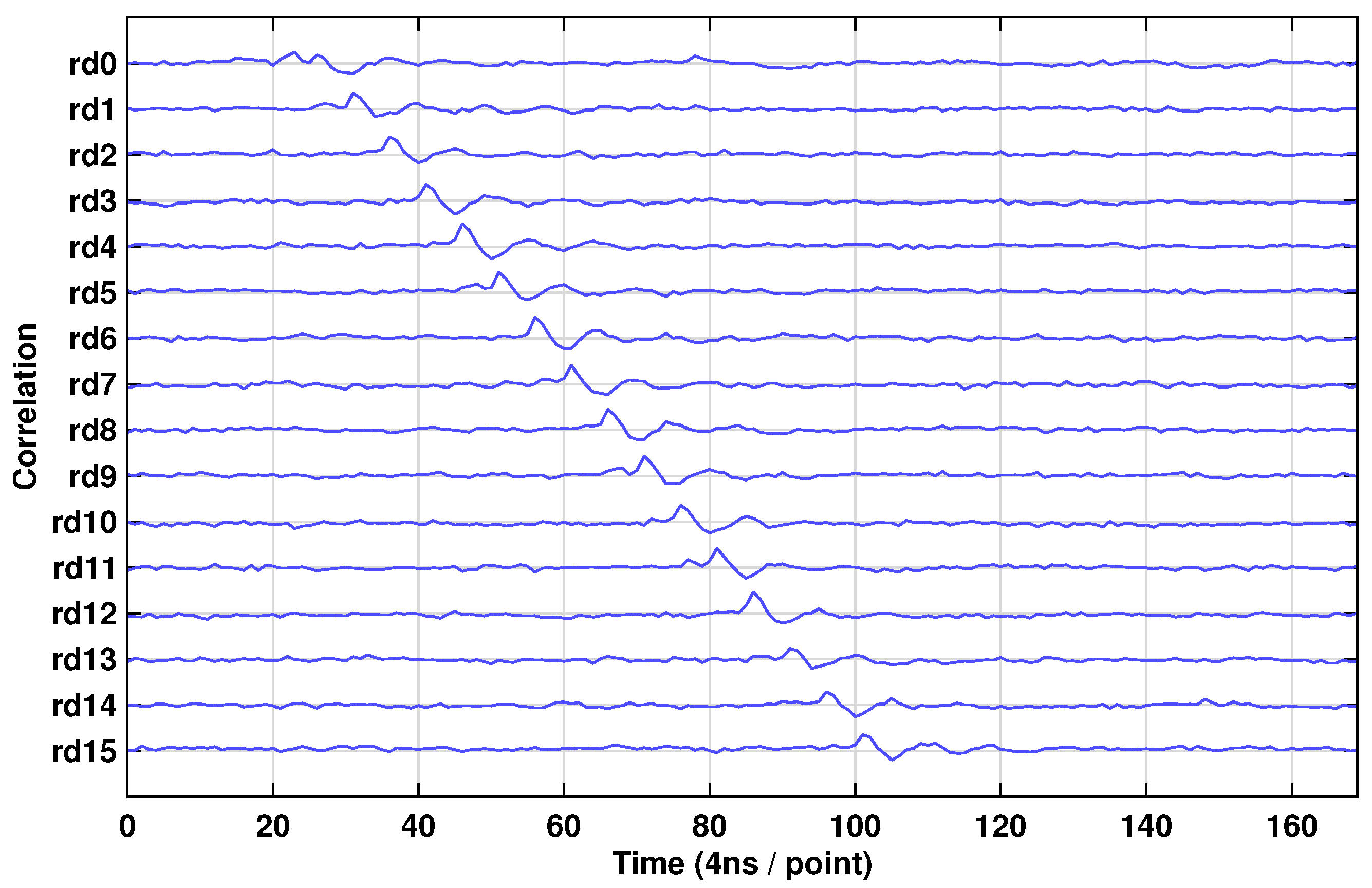
We first illustrate the CPA process on the FF-based implementation with 64 instances under the HD model. Figure 2 plots the correlation coefficients of the correct key for the 16 rounds driven by each 128-bit plaintext. Distinct correlation peaks are consistently observed for all 16 rounds, and their temporal ordering matches the expected operation sequence implied by the byte-serial scheduling described in Algorithm 3. This confirms that the sensor captures the repeated substitution activity and that each round provides an exploitable CPA target.
Algorithm 3: Device-level test procedure.
Electronics 15 01546 i003
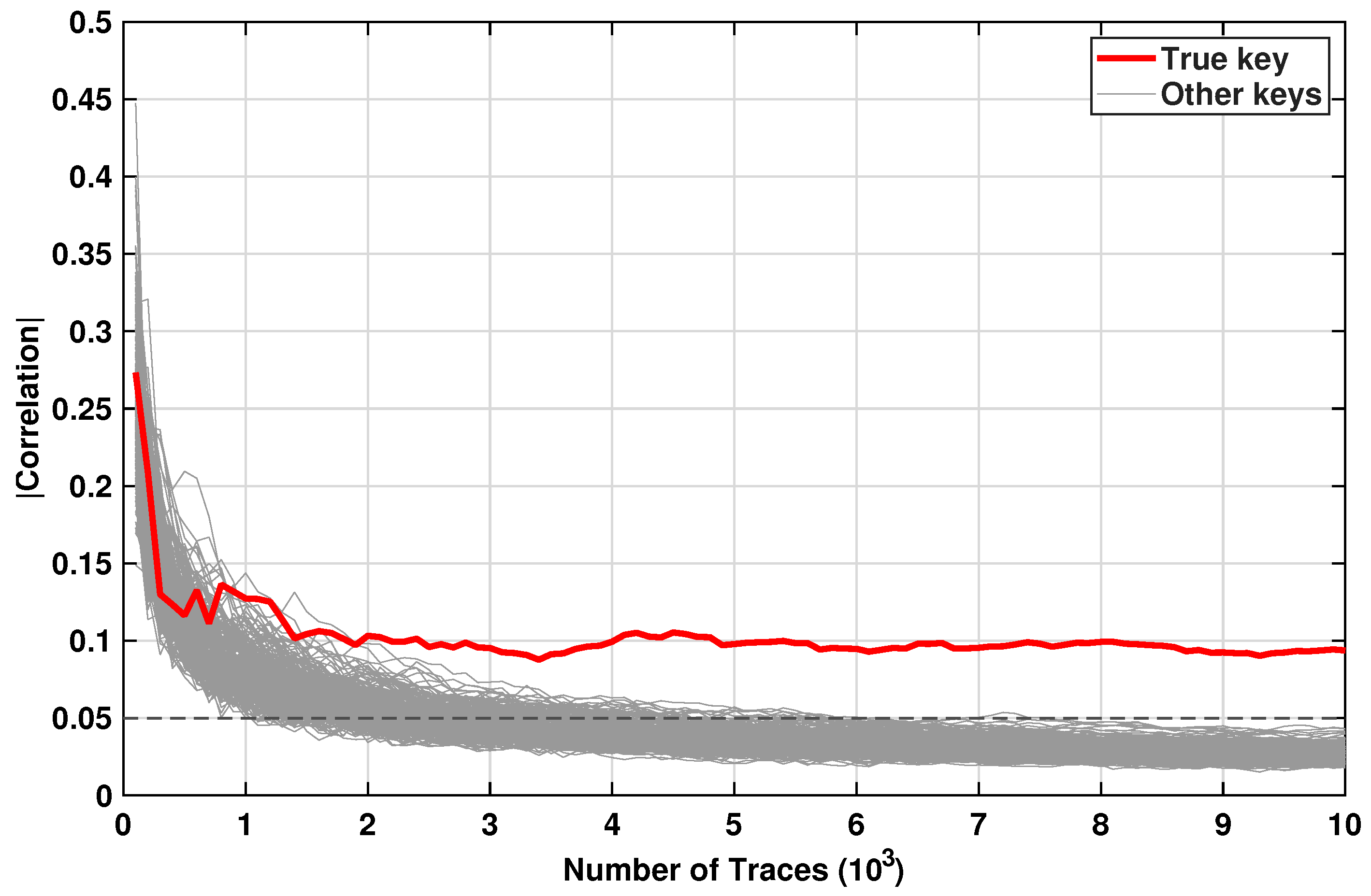
To further demonstrate the trace-driven convergence of CPA, Figure 3 shows the evolution of correlation as the number of trace increases for round 7. The red curve corresponds to the correct key hypothesis, while the gray curves correspond to the remaining 255 candidates. With an increasing number of traces, the correct key correlation separates from the bulk of incorrect hypotheses, and becomes distinguishable after approximately 2000 traces. We note that the correlations of incorrect key hypotheses typically remain within the range of 0 to 0.05, whereas configurations in which the correct key reaches rank 1 generally exhibit a correlation peak exceeding 0.05 with 10,000 traces. This empirical separation motivates the horizontal dashed line at 0.05 as a visual reference for distinguishability. And the dashed line is not used as a criterion for judging in any conditions. This observation is consistent with the key-ranking criterion described in Algorithm 1 and indicates that the FF-based implementation exhibits leakage under the HD model.
We next summarize the results across all experimental configurations by varying the FPGA primitive type and the number of instantiated devices, and by applying both the HW and HD models.
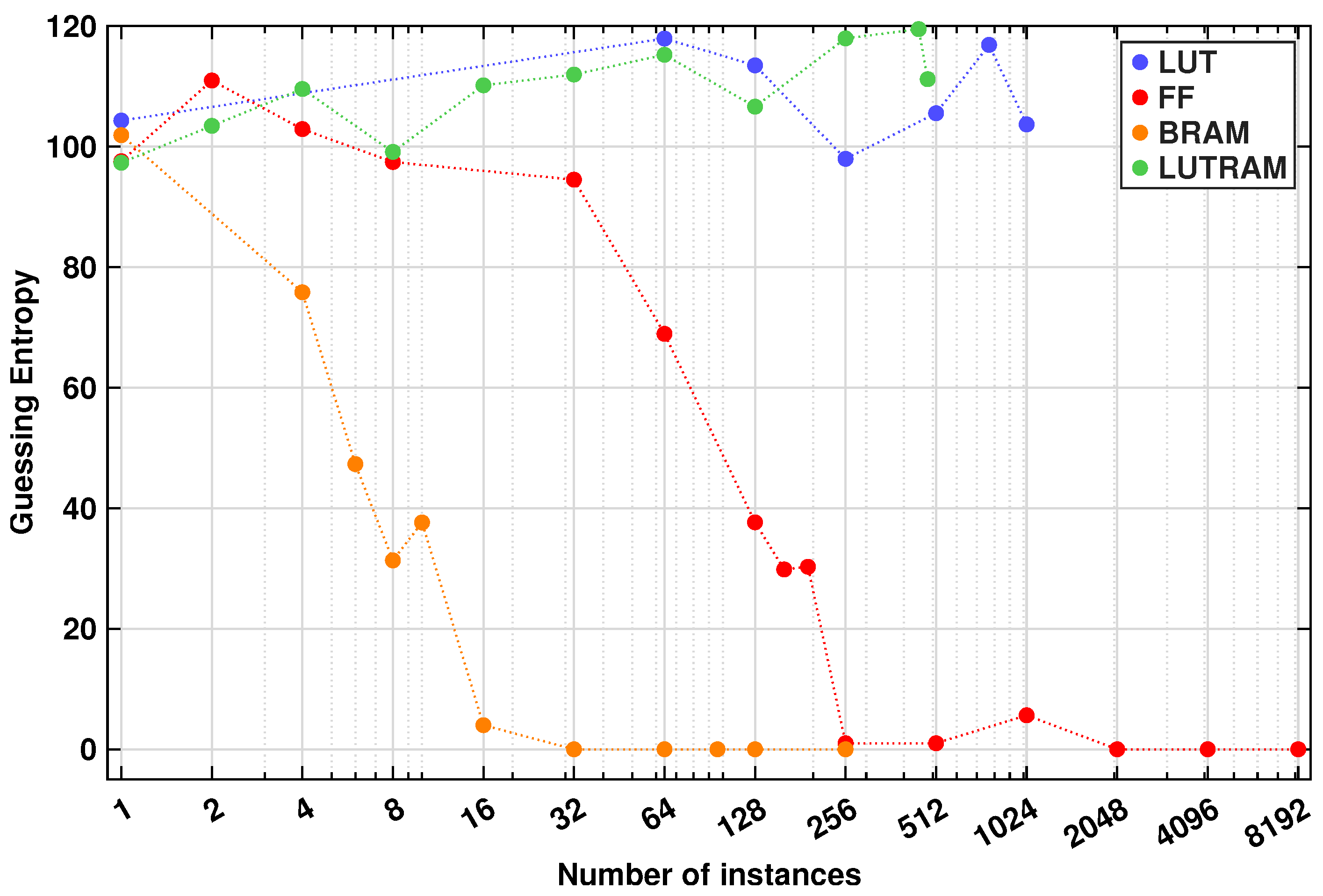
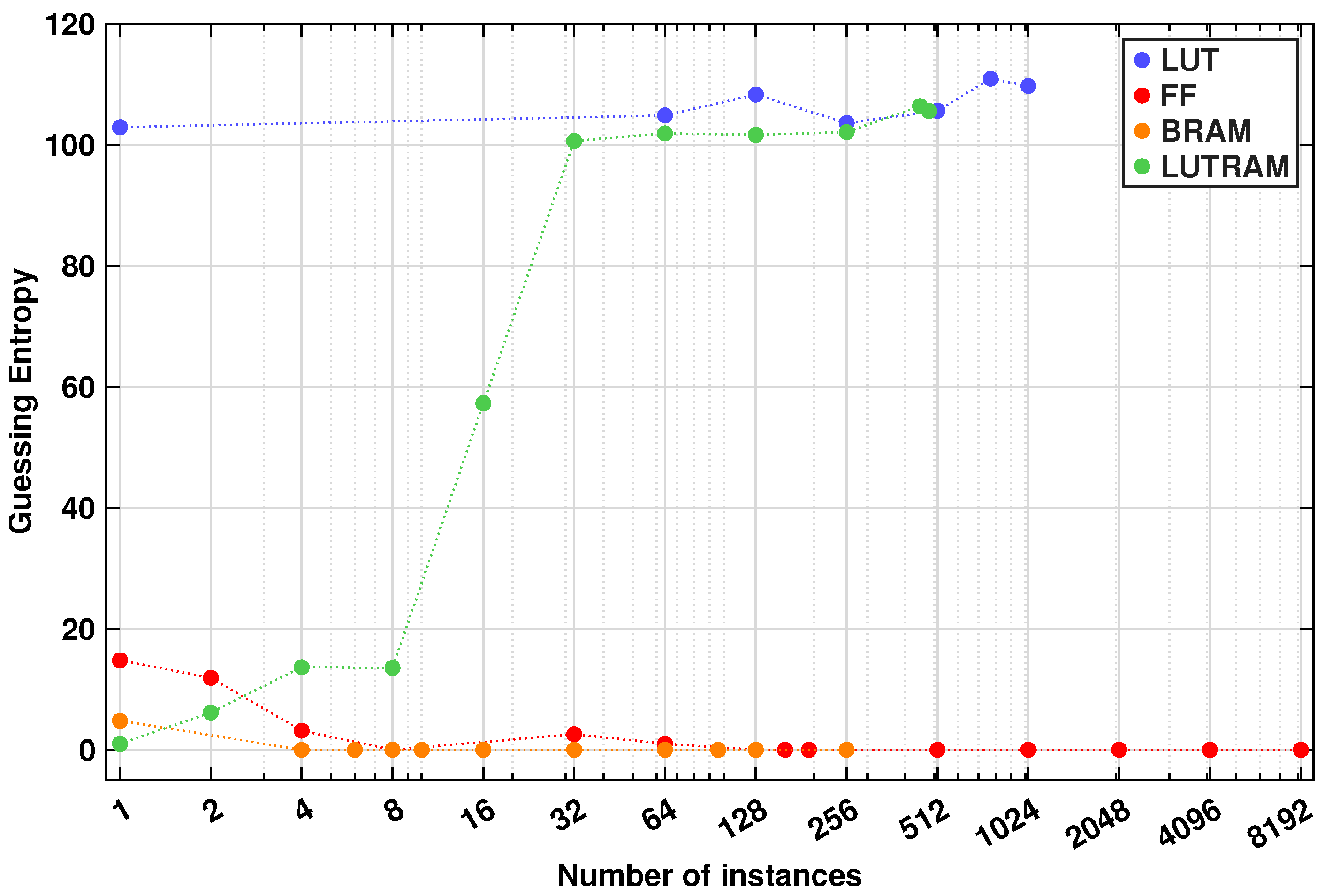
The Figure 4 and Figure 5 report the guessing entropy achieved under each configuration, summarizing key-recovery difficulty as the number of instantiated primitives increases. In this work, GE = 0 indicates successful recovery of all 16 independent 8-bit subkeys. For each 8-bit subkey, the guessing space is 2 8 = 256 candidates. Based on the definition in Equation (8), the theoretical maximum is reached when the correct key is ranked 256, yielding GE = i = 1 16 log 2 ( 256 ) = 128 .
Under the HW model (Figure 4), both LUT- and LUTRAM-based implementations exhibit GE values around ∼100 or higher, indicating that the correct key is rarely promoted to the top candidates and key recovery is practically ineffective. In contrast, BRAM- and FF-based implementations show a clear improvement with replication: GE decreases as the instance count increases. Specifically, BRAM reaches GE 4 at 16 instances and becomes GE = 0 for larger counts, while FF attains GE 1 at 256 and 512 instances, temporarily fluctuates to around 5, and then converges to GE = 0 and remains there. Overall, under the HW model, LUT and LUTRAM are difficult to break, whereas BRAM and FF become breakable once sufficient replication amplifies the leakage.
Under the HD model (Figure 5), LUT remains consistently above ∼100, again indicating non-recoverability within the evaluated trace budget. BRAM exhibits strong exploitability: GE is about 4.8 at a single instance and becomes 0 from 4 instances onward. FF shows a similar trend, with GE below 20 for 1–2 instances, dropping to about 3.2 at 4 instances, and then staying close to 0 for larger counts with some fluctuations at 32 and 64 instances. LUTRAM behaves differently: GE is 1 at 1 instance, implying near-complete recovery with only one byte remaining at rank 2; GE increases to about 6.2 at 2 instances and to about 13.5 at 4–8 instances, then rises sharply and exceeds 100 for larger counts. Therefore, under the HD model, LUT is still difficult to break, BRAM and FF are readily breakable, while LUTRAM is breakable only at small instance counts below 8 and becomes progressively harder to break as replication increases.
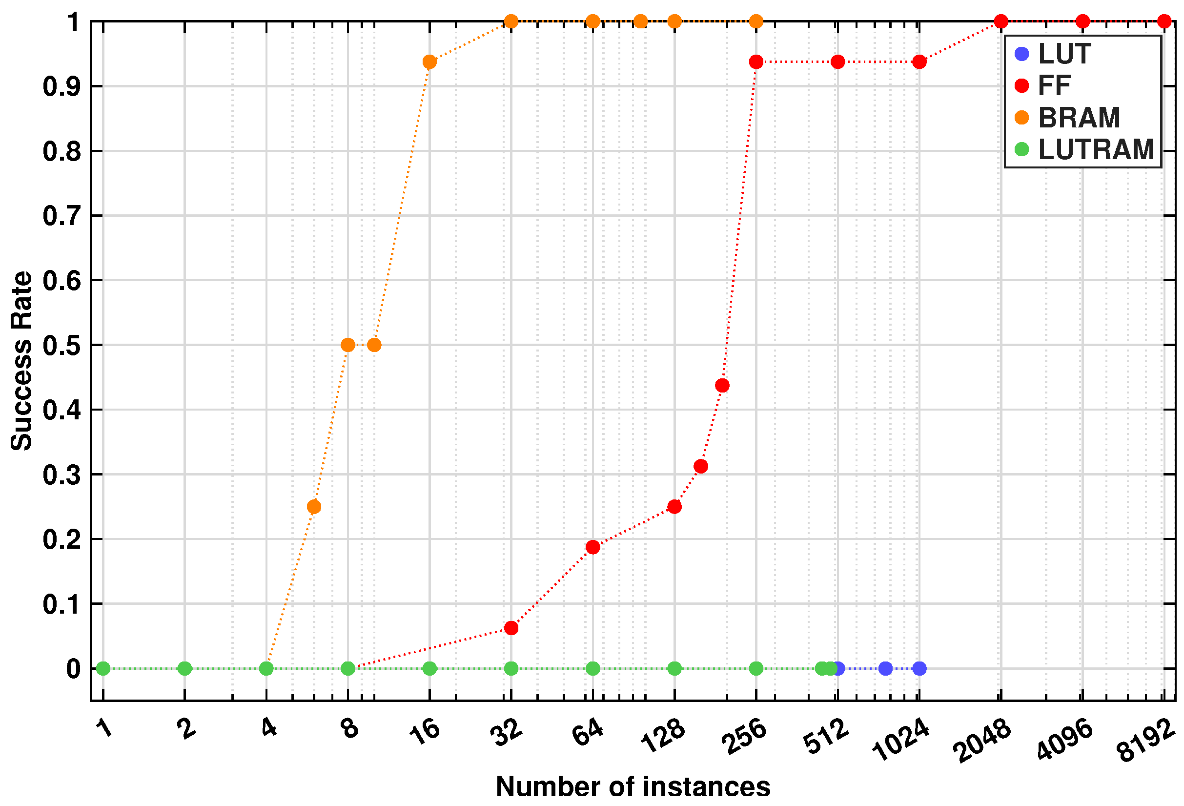
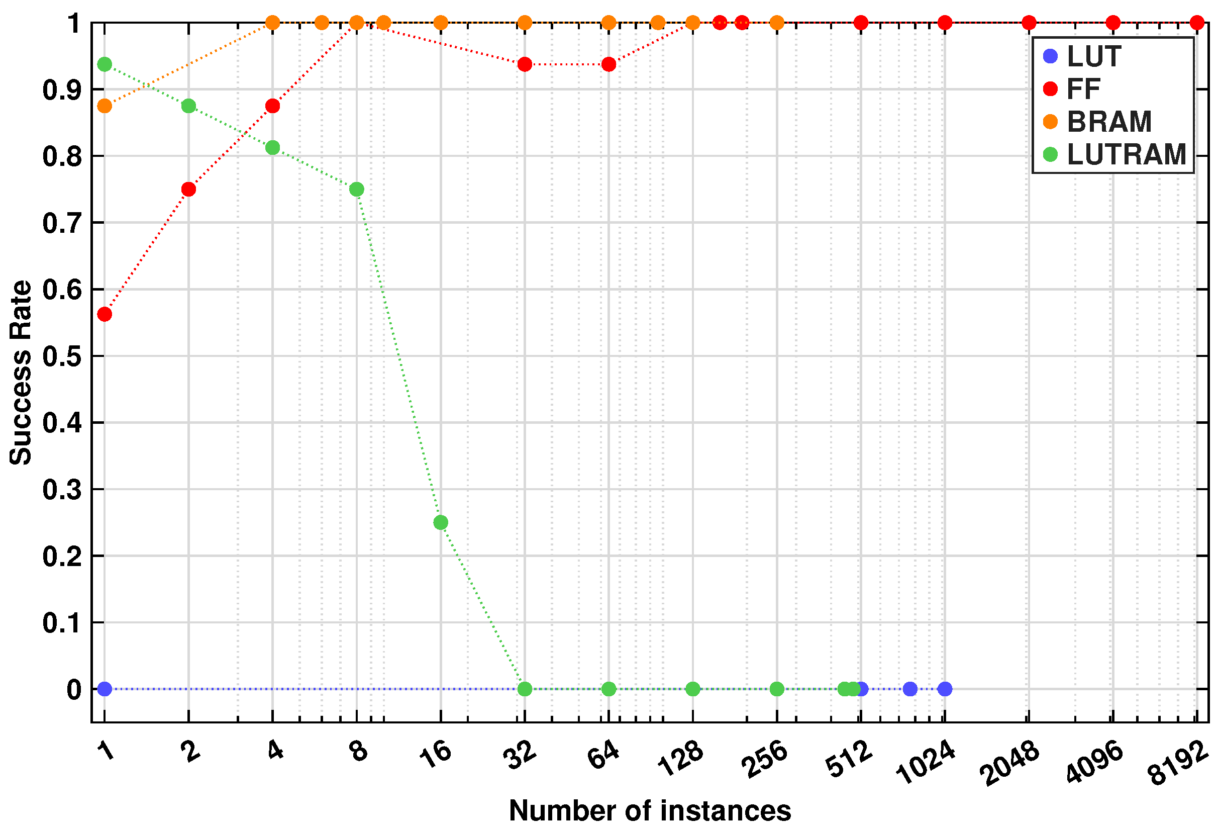
Figure 6 and Figure 7 present the CPA success rate for each experimental configuration under the HW and HD models respectively. Here, the success rate is defined as the fraction of correctly recovered 8-bit subkeys among the 16 independent targets at 10,000 traces.
Under the HW model (Figure 6), both LUT- and LUTRAM-based implementations remain at zero success rate across the tested instance counts, indicating that none of the 16 subkeys can be reliably recovered within the trace budget. In contrast, BRAM exhibits a monotonic replication gain: the success rate starts to increase from 4 instances, exceeds 0.9 at 16 instances, and reaches 1 for 32 instances and beyond. FF shows a similar but slower trend, with the success rate increasing from 8 instances, exceeding 0.9 at 256 instances, and stabilizing at 1 for 2048 instances and above.
Under the HD model (Figure 7), LUT again remains at zero success rate for all instance counts. BRAM achieves a success rate of 1 from 4 instances onward, and FF achieves a success rate of 1 from 8 instances onward, with only minor variations observed at 32 and 64 instances. LUTRAM demonstrates a strongly non-monotonic behavior: it attains a success rate above 0.7 for 1–8 instances, drops sharply to 0.25 at 16 instances, and becomes 0 for larger instance counts. Overall, from the success-rate perspective, the breakability trends across device types are consistent with the GE-based observations.
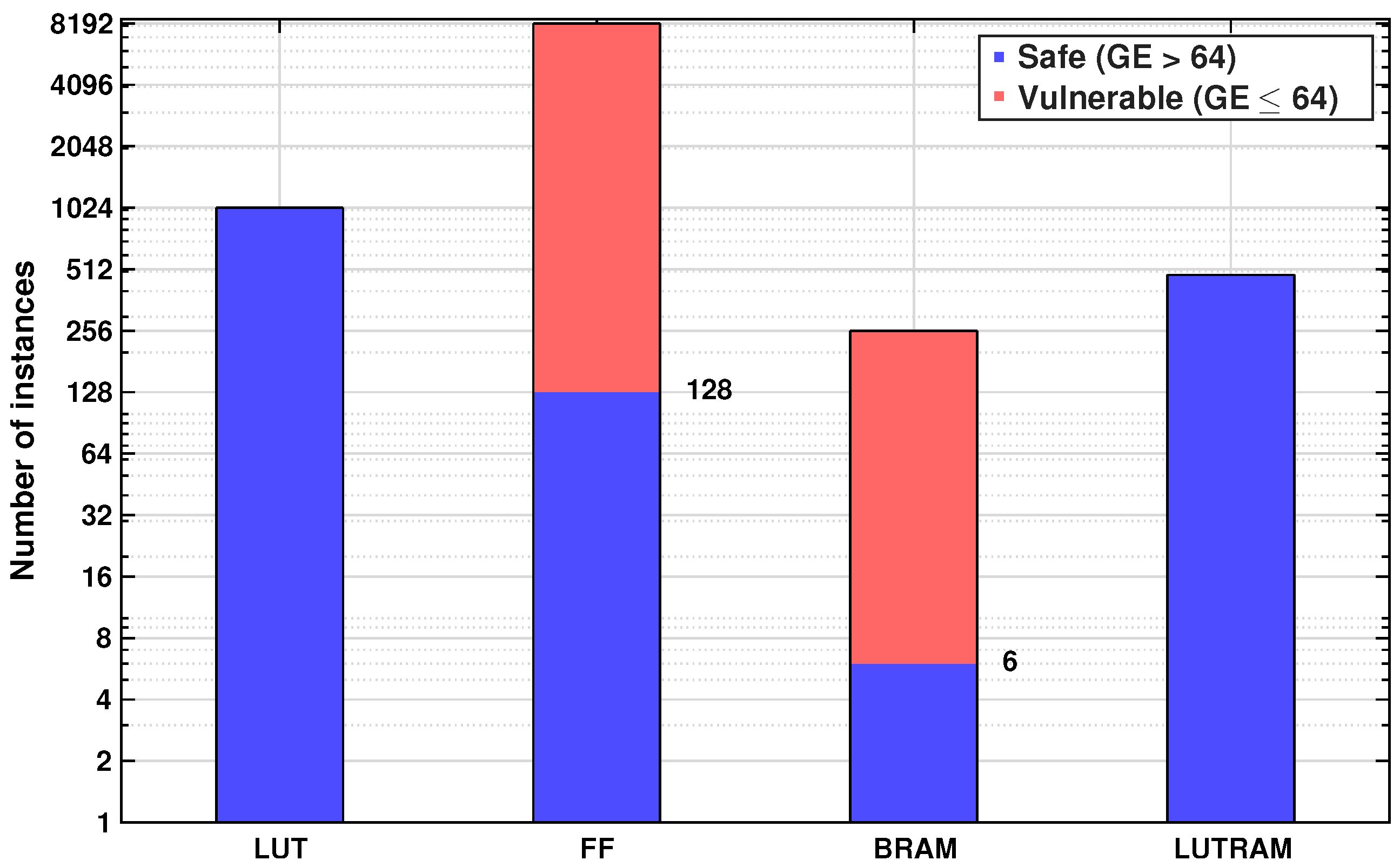
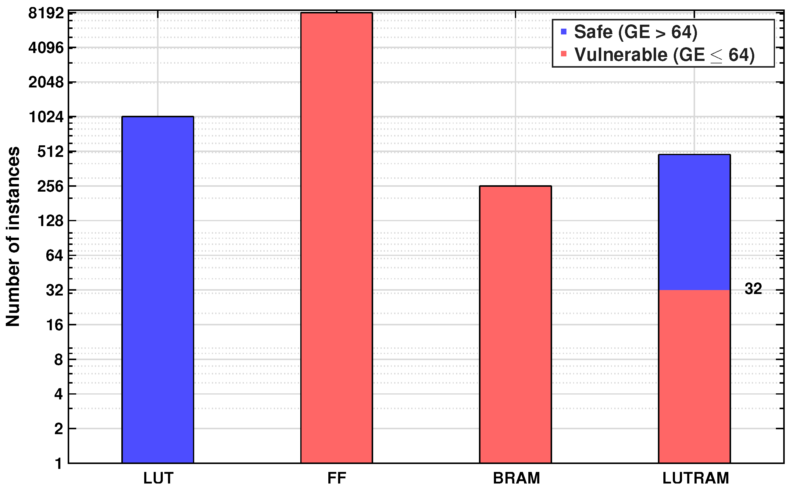
Figure 8 and Figure 9 summarize the attack outcomes across device types under the HW and HD models from a security-oriented perspective. As a practical security reference, a configuration is considered acceptable only if each 8-bit subkey cannot be reduced to a small candidate set under CPA. Specifically, we use “top-16” key ranking as a threshold: if the correct key byte is ranked within the top 16 candidates out of 256, the remaining brute-force effort for that byte is reduced from 2 8 to 2 4 . When all 16 key bytes are ranked within the top-16 set, Equation (8) yields GE = i = 1 16 log 2 ( 16 ) = 64 . Accordingly, the boundary GE = 64 is used to classify configurations: configurations with GE 64 are labeled as vulnerable, whereas those with GE > 64 are labeled as safe under the considered experimental conditions and trace budget.
As shown in Figure 8 and Figure 9, this criterion leads to a clear device-centric risk separation. Across both models, FF- and BRAM-based implementations more frequently fall into the vulnerable region, indicating a higher leakage risk and a lower residual key-search complexity once CPA is applied. In contrast, LUT-based implementations remain in the safe region in the evaluated configurations, suggesting that no clear exploitable leakage is observed for LUT under the present setup and analysis workflow. Overall, the success maps reinforce that the FPGA primitive used to realize a sensitive point is a dominant factor in practical side-channel analysis.
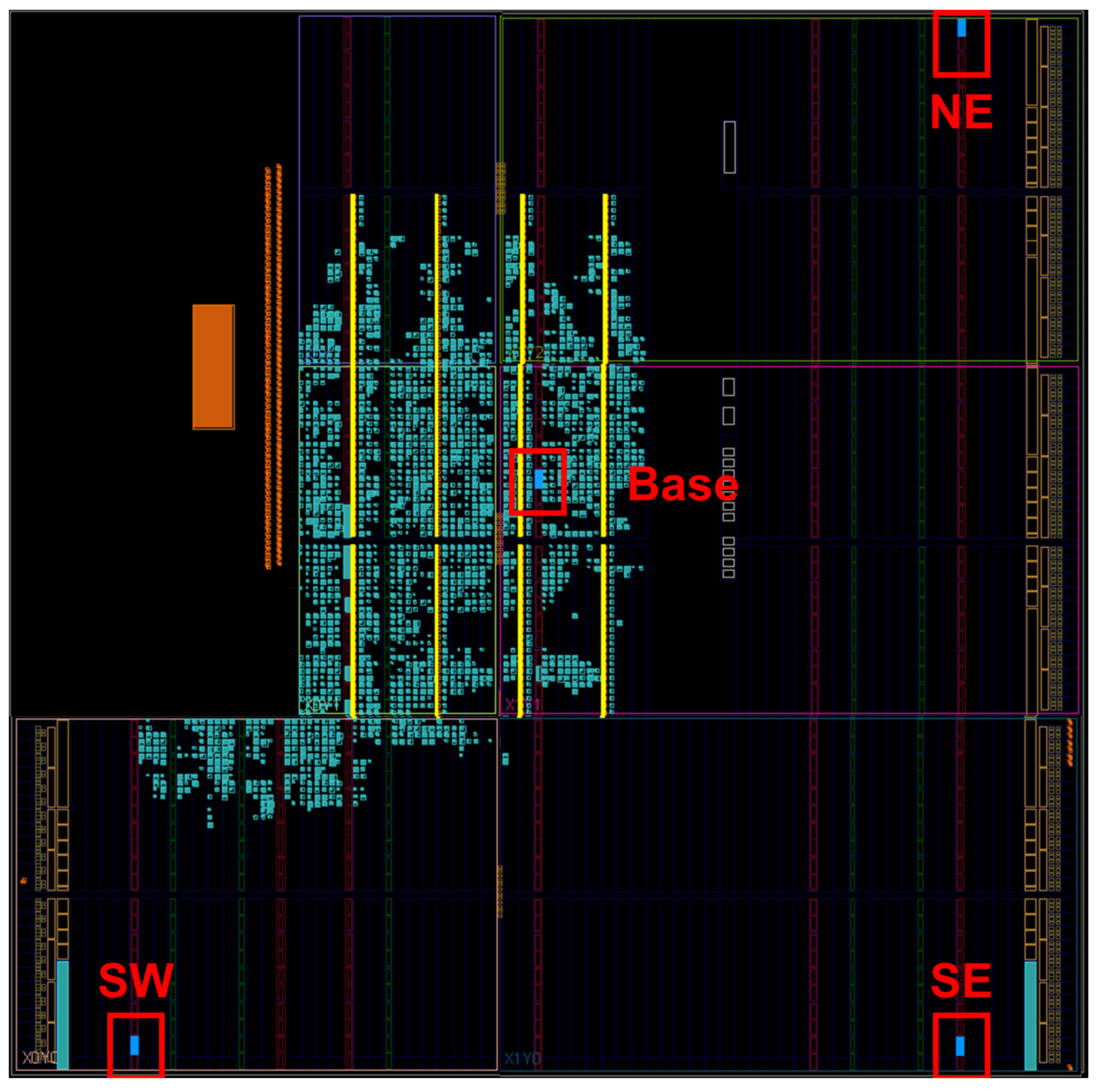
To assess the impact of placement on leakage behavior, we conduct a placement-variation experiment for the single-instance BRAM configuration. We use the original placement, where the BRAM instance is located close to the TDC sensor, as the baseline. As comparisons, we place the BRAM instance at three corners of the chip: north-east (NE), south-east (SE), and south-west (SW). Figure 10 illustrates the details: the red boxes mark four alternative placement locations, each corresponding to a candidate region for deploying the single BRAM instance. The small blue rectangles indicate the exact location in each region. In each experiment, only one location is activated and the BRAM is placed in exactly one of the marked regions.
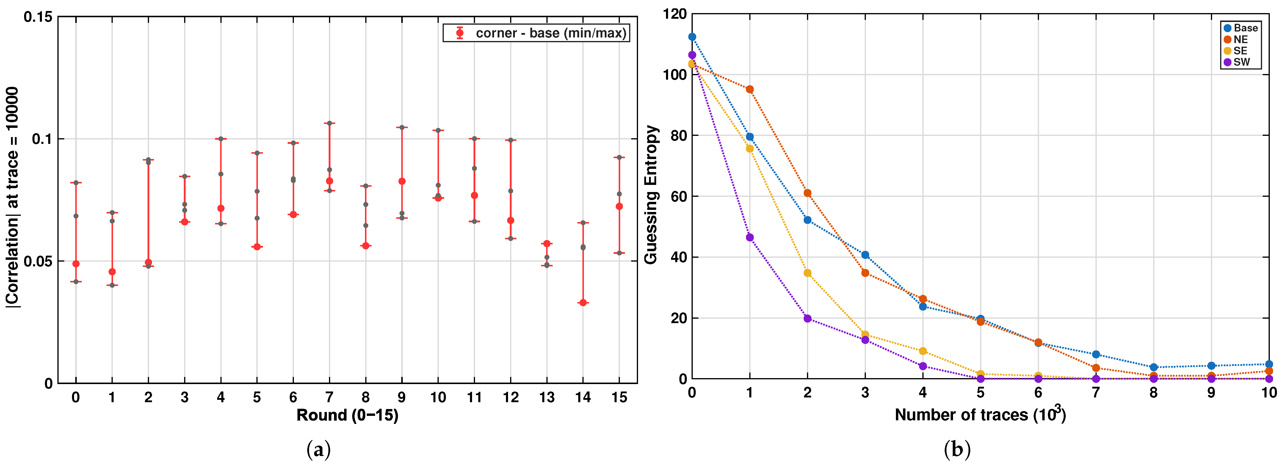
Figure 11a reports the correlation coefficient of the correct key after processing 10,000 plaintexts. The red dot indicates the baseline result, and the gray points represent the results for the corner placements. Figure 11b depicts the evolution of GE as a function of the number of plaintexts. Overall, the convergence trends are similar across placements; however, the corner placements yield lower GE than the baseline placement near the TDC. Specifically, the final GE values are GE = 2.58 for NE and GE = 0 for both SE and SW, whereas the baseline is GE = 4.81 . We attribute this difference to placement-induced sensing conditions: in the baseline case, the single BRAM instance is surrounded by other non-target logic in close proximity, which may attenuate or mask the voltage fluctuation attributable to the target instance, making its contribution less distinguishable in the sensed traces. In contrast, placing the instance in corner regions can reduce interference from nearby switching activity, thereby improving the observability of the target-induced voltage variations and leading to improved CPA convergence.

3.2. SM4 Encryption Case Study

According to the SM4 key schedule, the 128-bit original key can be derived once the first four round keys are recovered. Therefore, CPA is performed on the two SM4 encryption modules by targeting the first four round keys { RK 0 , RK 1 , RK 2 , RK 3 } . Each round key is 32 bits and consists of four bytes; consequently, the attack involves 16 independent 8-bit targets in total.
The two designs share the same SM4 architecture and differ only in the S-box implementation style (BRAM versus LUT), allowing us to isolate the impact of the underlying FPGA primitive on the attack outcome.
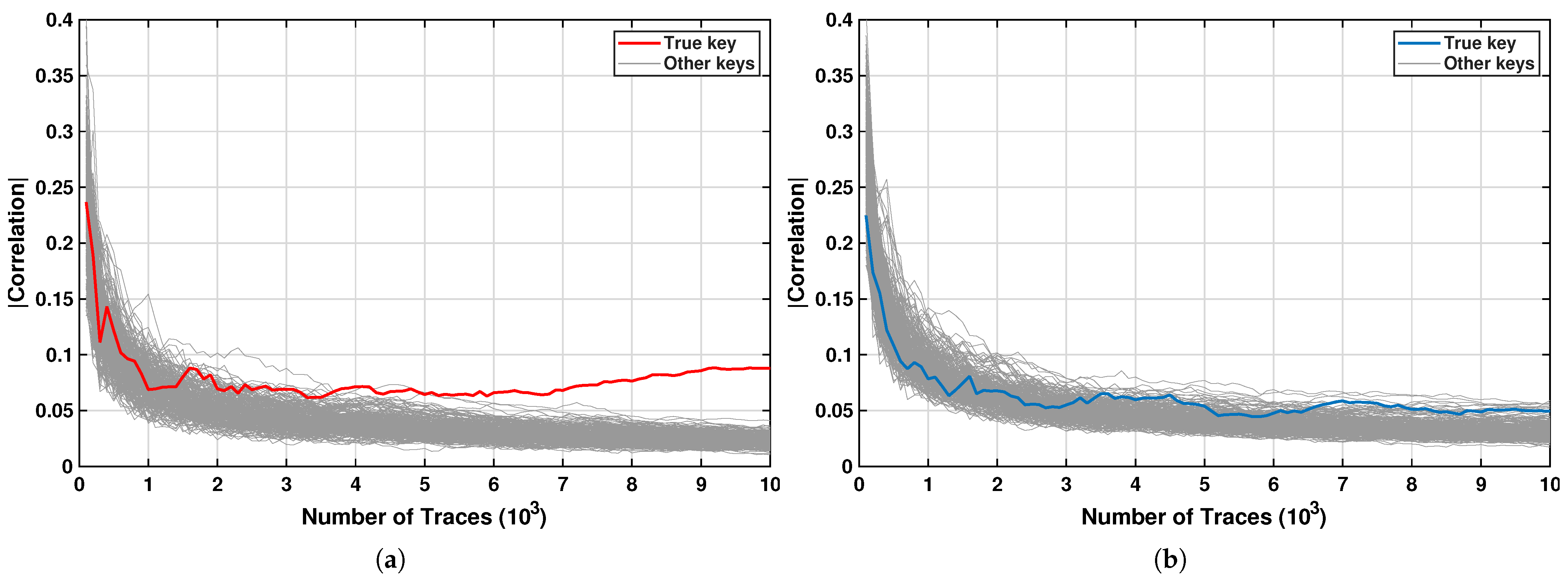
We take the first byte of the round key RK 0 to illustrate the CPA convergence process. Figure 12 shows the full CPA convergence process by plotting the correlation evolution as the number of analyzed plaintexts increases. In Figure 12a, the BRAM-based implementation becomes distinguishable after approximately 5000 traces. In Figure 12b, the LUT-based implementation remains indistinguishable even after the full set of 10,000 traces. We also observe that, for the LUT-based implementation, the correct key may occasionally enter the top-16 ranking; however, such events do not converge as the trace count grows, and the ranking exhibits a largely non-monotonic and seemingly random fluctuation.
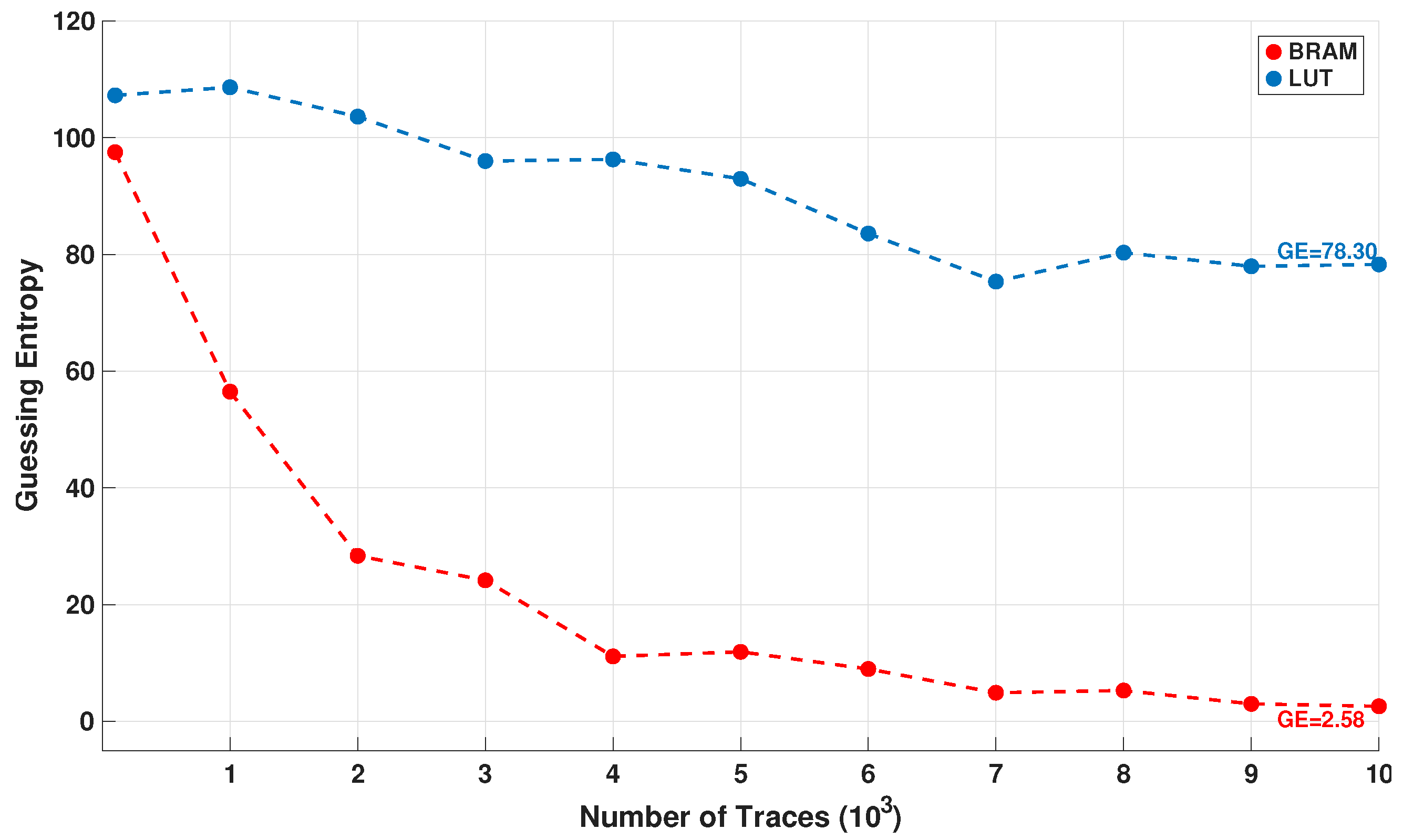
Taking all 16 targets into account, Figure 13 plots the evolution of guessing entropy as a function of the number of traces for the two SM4 implementations. For both designs, GE decreases as more traces are processed, indicating the expected trace-driven improvement of CPA. However, the convergence rates differ markedly across those two device types. For the BRAM-based implementation, GE drops rapidly and reaches approximately 11 around 4000 traces, and further decreases to 2.58 at 10,000 traces. According to the definition, GE = 2.58 corresponds to an average remaining key-candidate set of about 2 2.58 6 , implying that the residual brute-force effort is small and the implementation is practically easy to break under the present setup. In contrast, the LUT-based implementation exhibits only a mild decrease, and remains at GE = 78.3 after 10,000 traces, which indicates that the key ranks rarely approach the top candidates and that reliable key recovery is not achieved within the evaluated trace budget. Overall, Figure 13 confirms that mapping the SM4 S-box to BRAM yields substantially stronger and more exploitable leakage than mapping it to LUTs, consistent with the device-level observations.
The SM4 case study corroborates the device-level findings: once an algorithmic sensitive point is realized in hardware, the FPGA primitive used for its implementation plays a dominant role in determining the effectiveness of power side-channel analysis. In particular, mapping the S-box to BRAM results in a clearly more exploitable leakage signature than mapping it to LUTs under the same acquisition and analysis settings. So the choice of FPGA resource for implementing critical algorithmic components constitutes a crucial security design dimension that should be carefully considered in the development of FPGA-based secure cryptographic modules.

4. Conclusions

This work presents a device-centric study of FPGA power side-channel leakage. An experimental platform is built on a Zedboard, where the power-consuming logic and the power-sensing module are logically separated, and an S-box-like function is implemented using LUT, FF, BRAM, and LUTRAM to quantify how FPGA primitive types affect exploitable leakage under CPA. The results show pronounced leakage differences across device types: FF- and BRAM-based implementations exhibit substantially stronger leakage than LUT- and LUTRAM-based ones. In addition, the HD model is generally more effective than the HW model in the performed CPA evaluations, which is plausibly attributed to the fact that HD more closely matches CMOS switching activity at clock edges. To further validate the device-level findings on a practical cipher, CPA is conducted on two SM4 encryption modules that share an identical architecture and differ only in the S-box implementation style. Under the same acquisition conditions and trace budget, the BRAM-based SM4 implementation becomes distinguishable and enables an effective key-recovery progress, whereas the LUT-based implementation remains indistinguishable within 10,000 traces and exhibits non-convergent key-ranking behavior. Overall, these results confirm that, once an algorithmic sensitive point is realized in hardware, the FPGA primitive to which it is mapped can largely determine the effectiveness of power side-channel analysis. It is noted that the device-level experiments intentionally employ replication to study how leakage scales with the amount of devices. In real applications, such excessive replication is uncommon and a module is typically instantiated once. From this practical perspective, the single-instance results are particularly relevant: under the HD model, FF-, BRAM-, and LUTRAM-based implementations already exhibit non-negligible leakage risk at one instance, indicating that FPGA power side-channel vulnerability can manifest without replication. Therefore, the presented device-centric evidence supports the conclusion that practical FPGA designs may face power side-channel risks, especially when sensitive points are mapped to primitives that are empirically more leaky. This work also suggests a practical protection direction that complements conventional countermeasures: selectively implementing sensitive points using LUT-based logic, which shows low and non-exploitable leakage in the present evaluation, can improve resistance against CPA and thereby enhance the security of FPGA-based cryptographic designs.
Several limitations should be acknowledged. First, the analysis is conducted at the FPGA-primitive granularity, which is the finest level that can be explicitly constrained using the available tool flow; due to the limited disclosure of internal device details by vendors, lower-level micro-architectural leakage sources are not investigated in this work. Second, in this work we model power consumption with the HW and HD leakage models. While these two models are widely used and empirically effective in our evaluations, we do not consider other leakage models like multivariate models, and it remains unclear whether the same quantitative trends would hold under alternative modeling assumptions. Third, the experiments are performed on a Xilinx device; whether the same trends hold for Intel/Altera or other vendors’ FPGA families remains to be validated, although most modern FPGAs are built upon broadly similar fundamental resources.

Author Contributions

K.Z. was responsible for conceptualization, methodology, software, validation, formal analysis, investigation, data curation, visualization, and writing—original draft. C.W. was responsible for investigation, visualization, software, validation, and writing—original draft. T.S. was responsible for conceptualization, resources, supervision, project administration, funding acquisition, and writing—review and editing. All authors have read and agreed to the published version of the manuscript.

Funding

This research has been supported by National Key Research and Development Program of China (No. 2023YFB3611905).

Data Availability Statement

The data that support the findings of this study are available from the author upon reasonable request.

Conflicts of Interest

The authors declare no conflicts of interest.

References

  1. Putnam, A.; Caulfield, A.M.; Chung, E.S.; Chiou, D.; Constantinides, K.; Demmel, J.; Esmaeilzadeh, H.; Fowers, J.; PrashanthGopal, G.; Gray, J.; et al. A Reconfigurable Fabric for Accelerating Large-Scale Datacenter Services. In Proceedings of the 2014 ACM/IEEE 41st International Symposium on Computer Architecture; ACM: New York, NY, USA; IEEE: Piscataway, NJ, USA, 2014; pp. 13–24. [Google Scholar] [CrossRef] [Scilit]
  2. Chung, E.; Fowers, J.; Ovtcharov, K.; Papamichael, M.; Caulfield, A.; Massengill, T.; Liu, M.; Lo, D.; Alkalay, S.; Haselman, M.; et al. Serving DNNs in Real Time at Datacenter Scale with Project Brainwave. IEEE Micro 2018, 38, 8–20. [Google Scholar] [CrossRef] [Scilit]
  3. Gnad, D.R.E.; Oboril, F.; Kiamehr, S.; Tahoori, M.B. An Experimental Evaluation and Analysis of Transient Voltage Fluctuations in FPGAs. IEEE Trans. Very Large Scale Integr. (VLSI) Syst. 2018, 26, 1817–1830. [Google Scholar] [CrossRef] [Scilit]
  4. Kocher, P.; Jaffe, J.; Jun, B. Differential Power Analysis. In Proceedings of the Advances in Cryptology—CRYPTO’ 99; Wiener, M., Ed.; Springer: Berlin/Heidelberg, Germany, 1999; pp. 388–397. [Google Scholar] [CrossRef] [Scilit]
  5. Brier, E.; Clavier, C.; Olivier, F. Correlation Power Analysis with a Leakage Model. In Proceedings of the Cryptographic Hardware and Embedded Systems—CHES 2004; Joye, M., Quisquater, J.J., Eds.; Springer: Berlin/Heidelberg, Germany, 2004; pp. 16–29. [Google Scholar] [CrossRef] [Scilit]
  6. Zhao, M.; Suh, G.E. FPGA-Based Remote Power Side-Channel Attacks. In Proceedings of the 2018 IEEE Symposium on Security and Privacy (SP); IEEE: Piscataway, NJ, USA, 2018; pp. 229–244. [Google Scholar] [CrossRef] [Scilit]
  7. Schellenberg, F.; Gnad, D.R.E.; Moradi, A.; Tahoori, M.B. An Inside Job: Remote Power Analysis Attacks on FPGAs. IEEE Des. Test 2021, 38, 58–66. [Google Scholar] [CrossRef] [Scilit]
  8. Glamočanin, O.; Coulon, L.; Regazzoni, F.; Stojilović, M. Are Cloud FPGAs Really Vulnerable to Power Analysis Attacks? In Proceedings of the 2020 Design, Automation & Test in Europe Conference & Exhibition (DATE); IEEE: Piscataway, NJ, USA, 2020; pp. 1007–1010. [Google Scholar] [CrossRef] [Scilit]
  9. Zhang, X.; Yang, Y.; Zou, J.; Shen, Q.; Zhang, Z.; Gao, Y.; Wu, Z.; Carlson, T.E. AmpereBleed: Exploiting On-chip Current Sensors for Circuit-Free Attacks on ARM-FPGA SoCs. In Proceedings of the 2025 62nd ACM/IEEE Design Automation Conference (DAC); IEEE: Piscataway, NJ, USA, 2025; pp. 1–7. [Google Scholar] [CrossRef] [Scilit]
  10. Glamočanin, O.; Shrivastava, S.; Yao, J.; Ardo, N.; Payer, M.; Stojilović, M. Instruction-Level Power Side-Channel Leakage Evaluation of Soft-Core CPUs on Shared FPGAs. J. Hardw. Syst. Secur. 2023, 7, 72–99. [Google Scholar] [CrossRef] [Scilit] [PubMed]
  11. Tian, S.; Moini, S.; Wolnikowski, A.; Holcomb, D.; Tessier, R.; Szefer, J. Remote Power Attacks on the Versatile Tensor Accelerator in Multi-Tenant FPGAs. In Proceedings of the 2021 IEEE 29th Annual International Symposium on Field-Programmable Custom Computing Machines (FCCM); IEEE: Piscataway, NJ, USA, 2021; pp. 242–246. [Google Scholar] [CrossRef] [Scilit]
  12. Giechaskiel, I.; Szefer, J. Information leakage from FPGA routing and logic elements. In Proceedings of the 39th International Conference on Computer-Aided Design; ICCAD ’20; ACM: New York, NY, USA, 2020; pp. 1–9. [Google Scholar] [CrossRef] [Scilit]
  13. Provelengios, G.; Holcomb, D.; Tessier, R. Power Distribution Attacks in Multitenant FPGAs. IEEE Trans. Very Large Scale Integr. (VLSI) Syst. 2020, 28, 2685–2698. [Google Scholar] [CrossRef] [Scilit]
  14. Gnad, D.R.; Oboril, F.; Kiamehr, S.; Tahoori, M.B. Analysis of transient voltage fluctuations in FPGAs. In Proceedings of the 2016 International Conference on Field-Programmable Technology (FPT); IEEE: Piscataway, NJ, USA, 2016; pp. 12–19. [Google Scholar] [CrossRef] [Scilit]
  15. Zick, K.M.; Srivastav, M.; Zhang, W.; French, M. Sensing nanosecond-scale voltage attacks and natural transients in FPGAs. In Proceedings of the ACM/SIGDA International Symposium on Field Programmable Gate Arrays; FPGA ’13; ACM: New York, NY, USA, 2013; pp. 101–104. [Google Scholar] [CrossRef] [Scilit]
  16. Moini, S.; Deric, A.; Li, X.; Provelengios, G.; Burleson, W.; Tessier, R.; Holcomb, D. Voltage Sensor Implementations for Remote Power Attacks on FPGAs. ACM Trans. Reconfig. Technol. Syst. 2022, 16, 1–21. [Google Scholar] [CrossRef] [Scilit]
Figure 1. (a) TDC implementation and placement; (b) Floorplan of the power-consumption module and the TDC sensor.
Electronics 15 01546 g001
Figure 2. Correlation over time for all rounds. FF-based, 64 instances, HD model.
Electronics 15 01546 g002
Figure 3. The correlation changes with the number of traces. FF-based, 64 instances, HD model. The dash line at 0.05 serves as a visual reference.
Electronics 15 01546 g003
Figure 4. Guessing entropy for different devices under the HW model.
Electronics 15 01546 g004
Figure 5. Guessing entropy for different devices under the HD model.
Electronics 15 01546 g005
Figure 6. Success rate for different devices under the HW model.
Electronics 15 01546 g006
Figure 7. Success rate for different devices under the HD model.
Electronics 15 01546 g007
Figure 8. Cases of different devices under the HW model.
Electronics 15 01546 g008
Figure 9. Cases of different devices under the HD model.
Electronics 15 01546 g009
Figure 10. Different placements of the single BRAM instance.
Electronics 15 01546 g010
Figure 11. (a) Correlation of the correct key for different placements; (b) Guessing entropy evolution for different placements.
Electronics 15 01546 g011
Figure 12. Correlation of the correct key vs. number of traces for SM4 RK0 byte 0 under (a) BRAM and (b) LUT implementations.
Electronics 15 01546 g012
Figure 13. Guessing entropy for the two SM4 implementations.
Electronics 15 01546 g013
Table 1. Different design styles and their maximum implementation device counts.
Design FormImplementation DeviceMaximum Number of InstancesMaximum Number of Devices
LUTLUT6102440,960
FFFDRE819265,536
BRAMRAMB18E1256128
LUTRAMRAM256X1S48015,360
Disclaimer/Publisher’s Note: The statements, opinions and data contained in all publications are solely those of the individual author(s) and contributor(s) and not of MDPI and/or the editor(s). MDPI and/or the editor(s) disclaim responsibility for any injury to people or property resulting from any ideas, methods, instructions or products referred to in the content.