1. Introduction
With the decreasing size and increasing efficiency of communication devices, there is a growing need for non-invasive antenna solutions [
1,
2]. Flexible and transparent antenna designs offer effective low-profile solutions for Internet of Things (IoT) applications, wearable electronics, smart surfaces, and space-constrained CubeSat platforms [
3,
4]. However, one of the challenges faced by researchers is to achieve an optimal balance between optical clarity and RF performance.
Conductive materials, such as Transparent Conductive Oxides (TCOs), silver nanowire (AgNW)-based solutions, graphene, and Indium Tin Oxide (ITO), have been studied. Each of these materials has specific limitations [
5,
6,
7]. In recent years, advanced fabrication techniques, such as Aerosol Jet printing and screen printing, have allowed for precise patterning on flexible substrates and improved optical transmittance [
8,
9].
Transparent antennas have demonstrated adequate performance in the 2.4–6 GHz frequency bands [
10,
11]. Furthermore, mid-band 3–6 GHz capabilities have been demonstrated with circular polarization [
12], wideband fractal slots [
13], transparent MIMO configurations [
14], and dual-band structures for Wi-Fi 6E [
15]. Reviews also highlight that material selection, mechanical stability, and system-level integration are important considerations for sub–6 GHz 5G applications [
16,
17,
18]. Although significant advances have been made toward achieving high levels of optical transmittance, flexibility, and reliable RF performance in the mid-band, simultaneously achieving all three of these attributes remains a significant challenge [
19].
To address this challenge, in this study, we present a transparent antenna designed for the 3–6 GHz band. It was fabricated using Aerosol Jet® 5X technology on a flexible polyimide substrate. In contrast to conventional approaches, this method affords higher levels of mechanical flexibility and optical transparency. The measured data closely correspond with the simulation results. The proposed antenna design is suitable for applications in various low-profile conformal communication systems.
The following is a summary of the contributions of this study:
Innovative Fabrication: Realization of a high-precision metal mesh with reliable RF performance and 85% light transmission through Aerosol Jet® printing.
Conformal Robustness: Verification of performance under bending conditions to demonstrate applicability for wearable applications.
System-Level Integration: Demonstration of compatibility with self-powered Internet of Things (IoT) platforms, wherein the antenna shows negligible impact on the efficiency of commercial solar cells.
2. Antenna Configuration and Design Guidelines
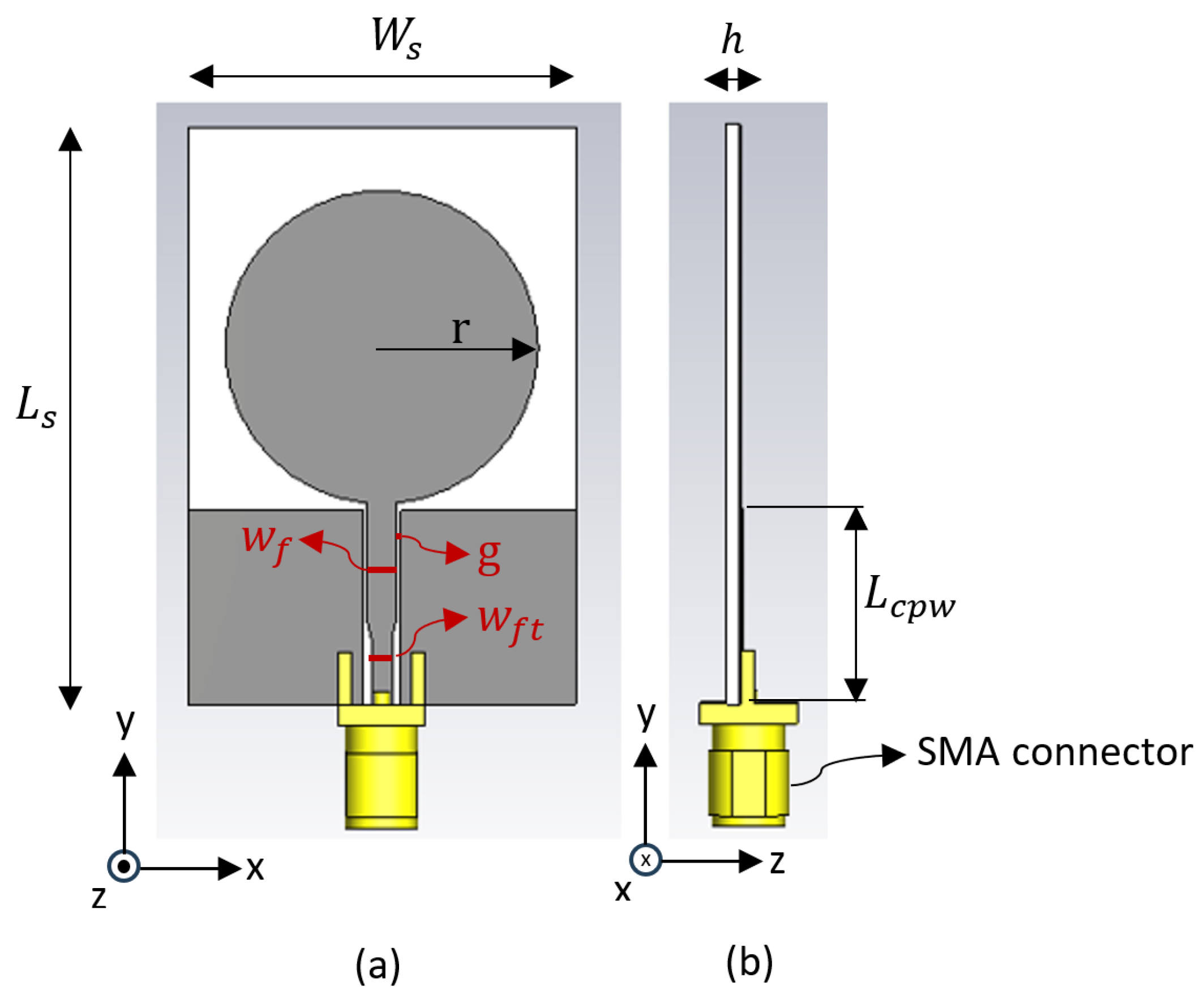
A circular monopole configuration (see
Figure 1) was selected to achieve a wide impedance bandwidth and omnidirectional radiation. This behavior is attributed to the ability of the circular radiator to support multiple current paths, which leads to multiple resonant modes. The antenna dimensions listed in
Table 1 were determined based on the quarter-wavelength principle commonly used in monopole antenna design [
20].
Modeling the ultra-thin substrate and the complex conductive grid pattern would cause an excessively dense computational mesh, resulting in prohibitive simulation times. Therefore, the simulations were performed using an equivalent continuous fully metallic structure.
Subsequently, these physical parameters were carefully optimized while considering the target frequency band using CST Microwave Studio to achieve the desired impedance matching. The antenna was excited via a waveguide port, and open (add space) boundary conditions were applied to emulate free-space radiation. Additionally, a magnetic symmetry plane (yz plane) was employed to reduce the computational domain.
A polyimide (, ) substrate was used due to its availability, optical transparency, and flexibility. To use it in wearable applications, a thin substrate thickness of 50 μm was selected. The gap (g) was set to 0.20 mm and the signal line width () to 2.20 mm to achieve a 50 impedance match. An SMA connector was included in the simulation to improve the agreement between simulated and measured results. To prevent a short circuit during the bonding of the SMA connector to the antenna using conductive adhesive, the signal line width was tapered from to .
3. Fabrication Process via Aerosol Jet Printing
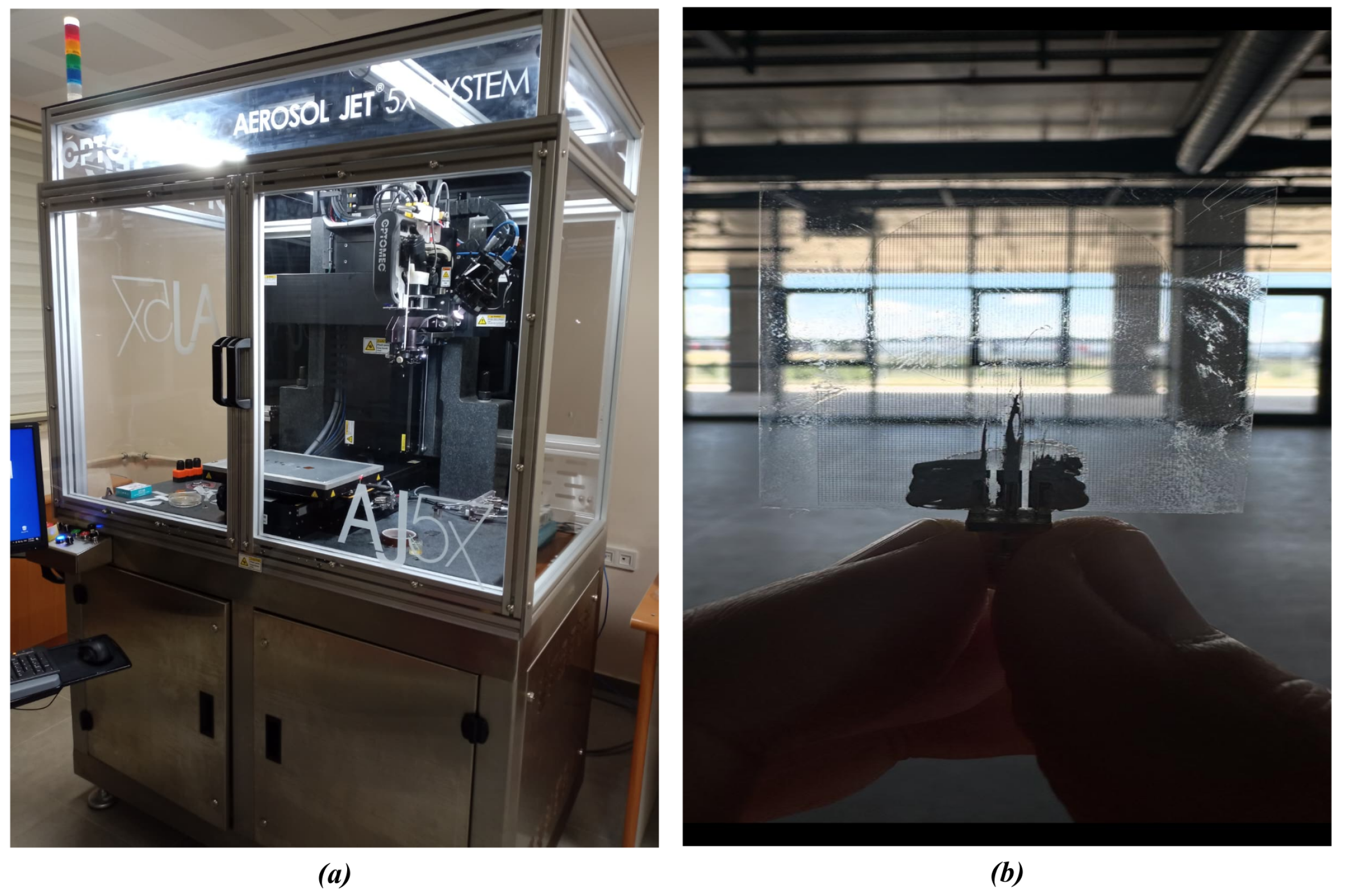
An Aerosol Jet
® 5X system (OPTOMEC, Albuquerque, NM, USA,
Figure 2a), which precisely deposits atomized conductive inks (Novacentrix Metalon
® JS-A426, Novacentrix, Austin, TX, USA) onto the substrate, was used for fabrication. The polyimide surface was cleaned with isopropanol before the printing process and was dried with nitrogen gas to provide suitable surface conditions.
The ultrasonic atomizer converted the ink into micron-level droplets, which were transferred onto the substrate by focusing through a 150 μm diameter nozzle. The gas flow rates were set to 9 sccm for the atomizer, 45 sccm for the sheath, 30 sccm for the divert flow, and 30 sccm for the boost flow. The printing speed was kept constant during the process, and the entire process was completed within 1.5 h. In order to obtain a homogeneous mesh structure and achieve a stable jet, printing parameters were optimized. Without waiting for any time gap, fabricated antennas were thermally annealed to facilitate sintering, which increases the electrical connectivity for 1 h at 150 °C.
The fabricated antenna prototype is presented in
Figure 2b. The mesh line width was approximately 30 μm, whereas the unit cell spacing was 250 μm. To ensure that the connector was aligned and did not create a short circuit on the low-adhesion polyimide surface, it was bonded using a silver adhesive and a custom mold. The gap between the signal line and the ground plane was kept as clear as possible to minimize impedance mismatch.
4. Experimental Validation and Discussion
4.1. Reflection Coefficient and Radiation Patterns
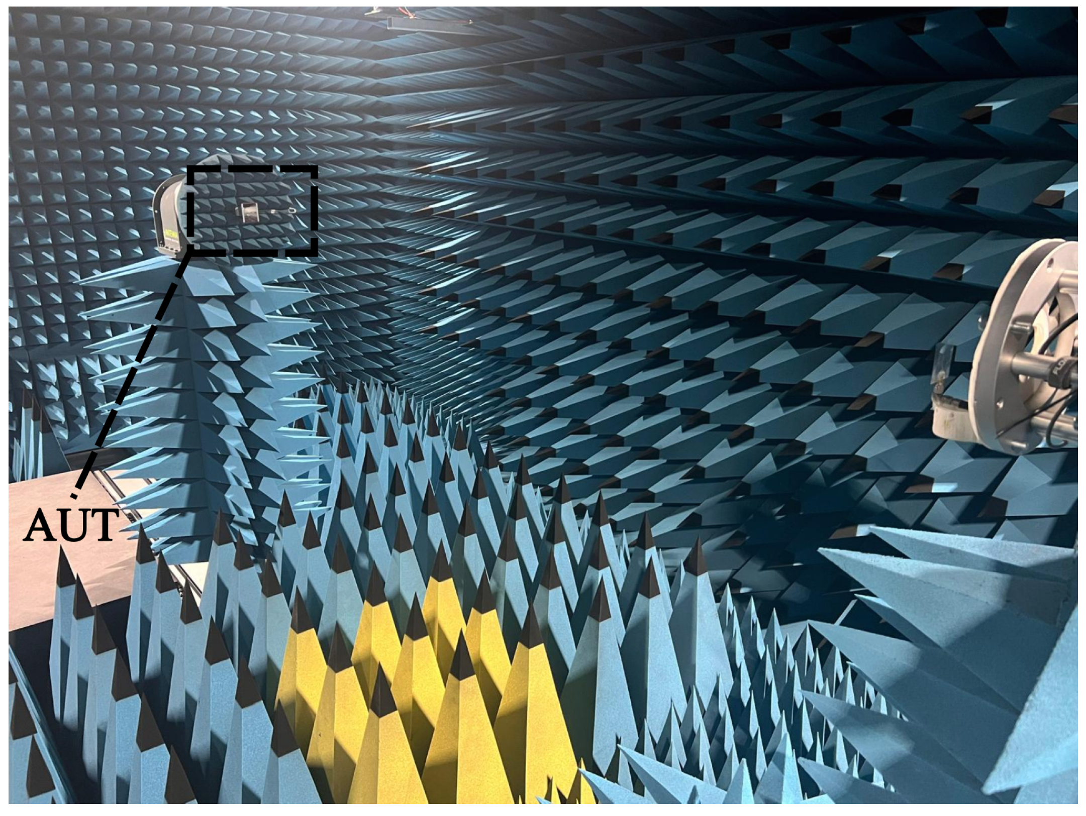
The reflection coefficient (
) of the antenna was obtained using a VNA, and the radiation pattern was measured in an anechoic chamber (
Figure 3). The maximum realized gain of the antenna was
dBi.
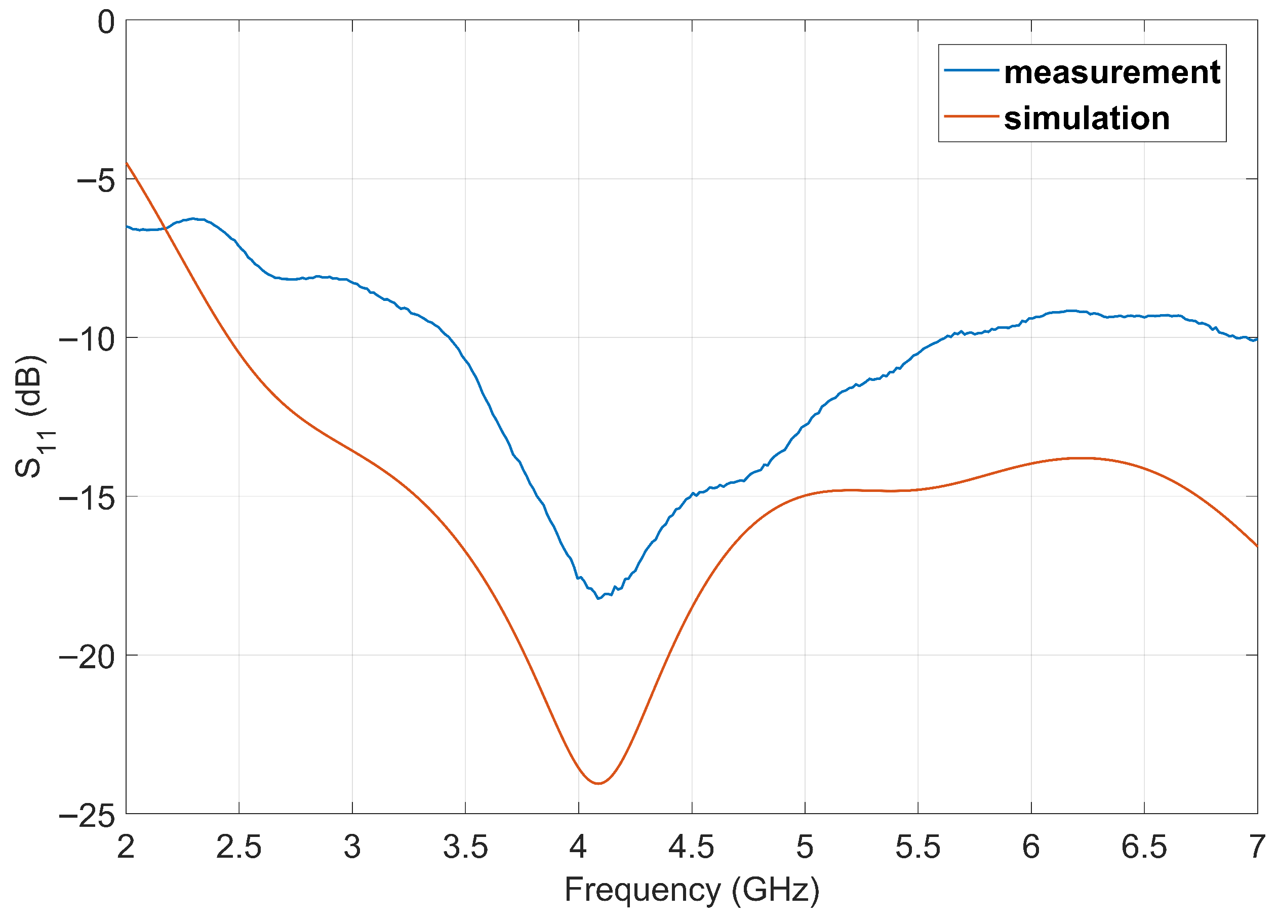
The measured and simulated
results are in good agreement, as shown in
Figure 4, confirming the validity of the design and simulation model.
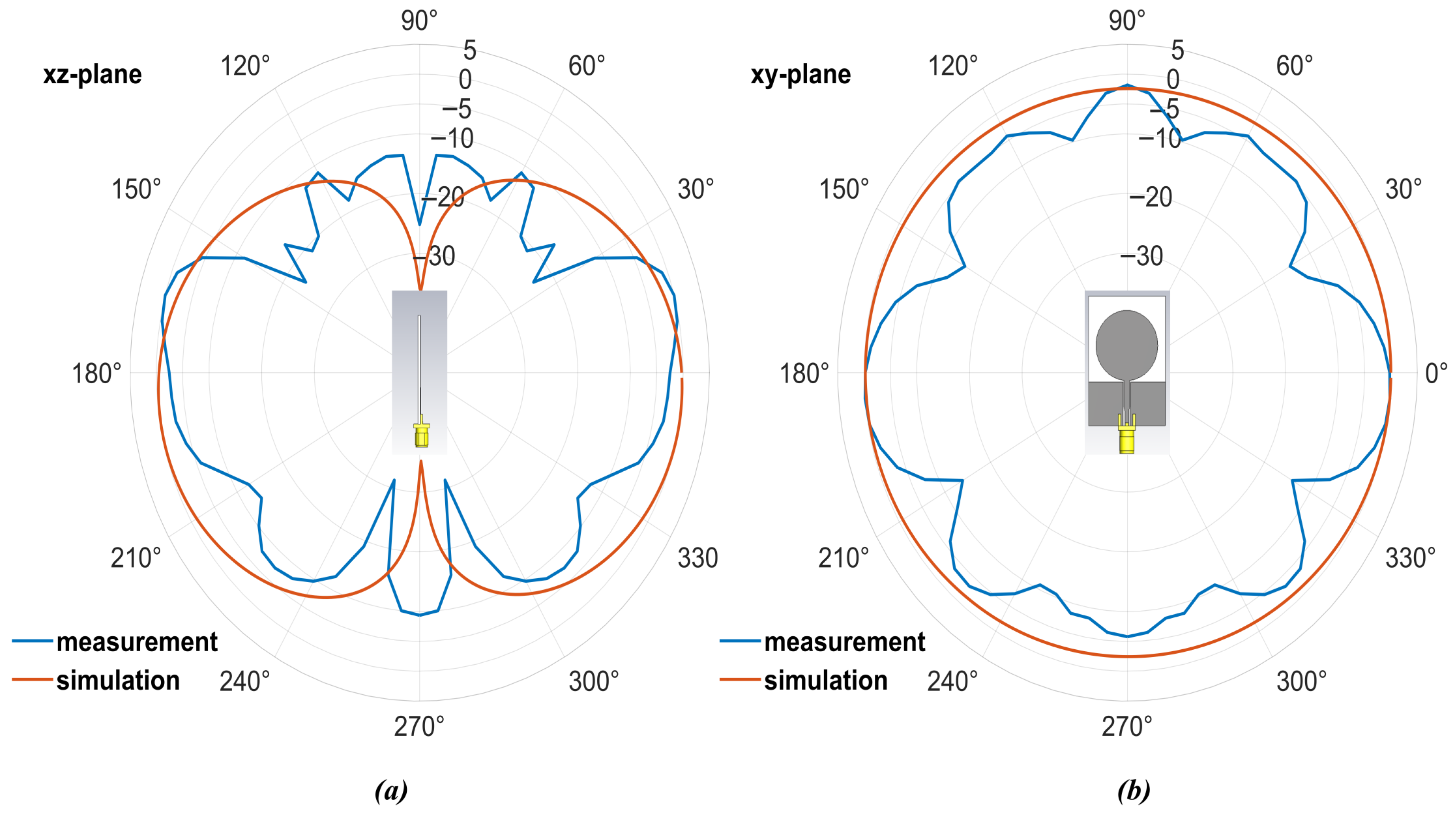
Small deviations are observed in the measured radiation patterns, particularly in the null regions at
and
(
Figure 5a). These deviations are attributed to the experimental setup. In particular, the metallic rotator and the relatively large SMA connector, in comparison to the 50 μm thick substrate, introduced unintended reflections and additional scattering.
Despite these effects, radiation patterns in both planes behave similar with the theoretical expectations in general. This shows the antenna’s performance stability and design validity.
4.2. Gain and Total Efficiency of the Proposed Antenna
To determine whether the antenna exhibits acceptable radiative properties and to validate the measured realized peak gain of
dBi, we evaluated the radiation efficiency of the proposed transparent antenna. A key factor in determining the loss mechanisms within the antenna is the effective sheet resistance (
) of the 2D square mesh structure. According to effective medium theory for metallic meshes [
21], the effective sheet resistance of the 2D metallic mesh can be modeled based on the resistivity of the intrinsic continuous conductive trace (
) and the geometric optical transparency (
). Thus,
The antenna was printed onto a flexible polyimide substrate using an Aerosol Jet printing system with a silver nanoparticle (AgNP) ink. Flexible polymers have thermal limitations, and therefore low-temperature sintering requirements limit the conductivity of the printed metal. Literature reports indicate that the typical sheet resistance of temperature-sintered AgNP films deposited onto flexible substrates ranges from 1.5 to 20
/sq [
22]. Therefore, for a high geometric optical transparency of the fabricated mesh (
), the estimated effective sheet resistance of the antenna structure is approximately
.
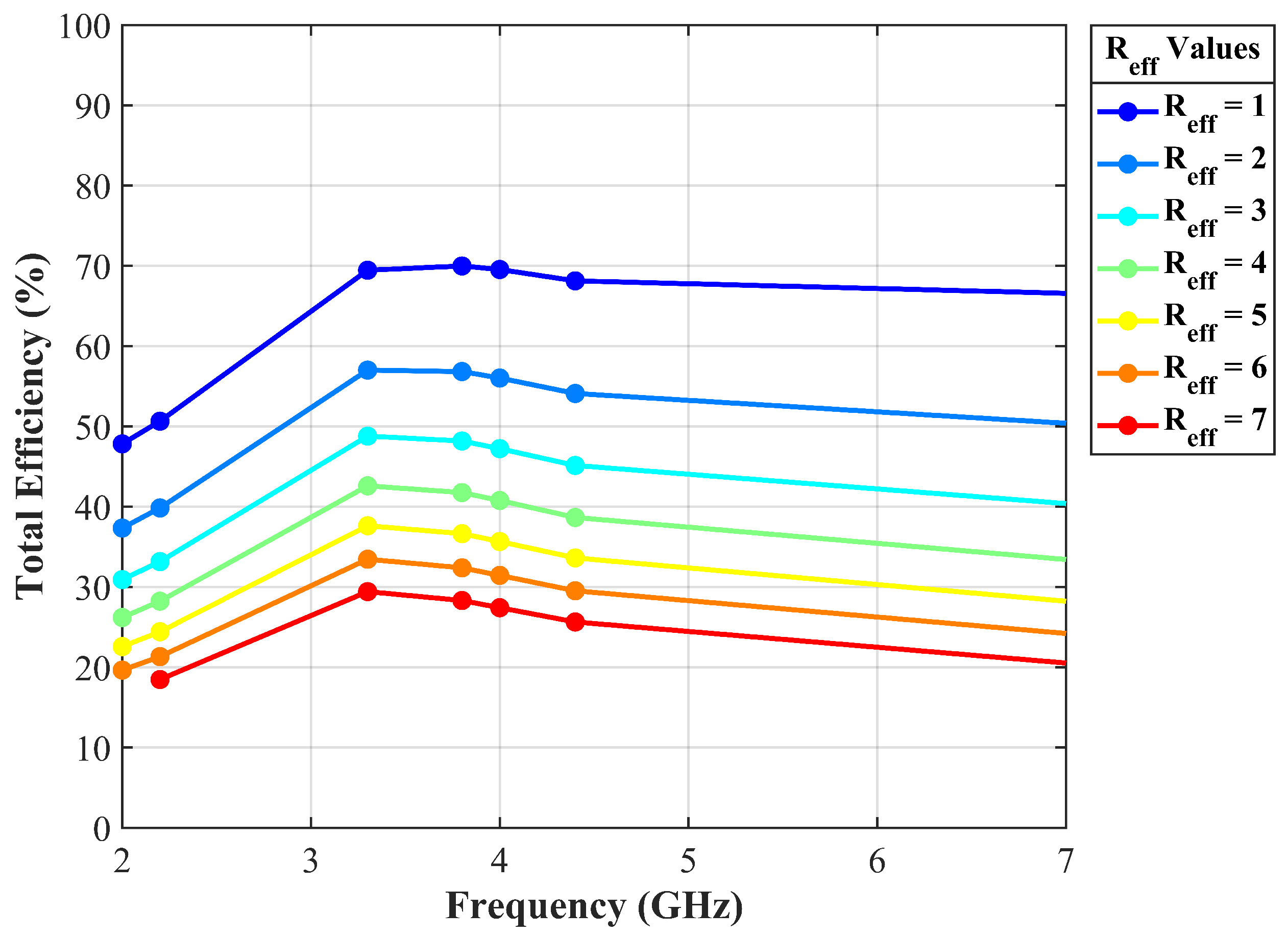
To quantify how mesh losses affect the radiation efficiency of the antenna, a series of parametric studies was conducted. The effective sheet resistance of the antenna mesh was varied in CST Microwave Studio, and the simulated total efficiency versus frequency was obtained (
Figure 6). As expected, increasing the effective sheet resistance reduces the efficiency due to increased ohmic losses associated with higher optical transmittance. Using the calculated value of
, the simulated radiation efficiency of the antenna at the resonant frequency is approximately 30%. The observed peak in total efficiency around 3.2 GHz is attributed to the primary resonant mode of the circular monopole, where the impedance matching is most effective. As the frequency increases, the slight decline in efficiency is a consequence of frequency-dependent ohmic losses within the silver nanoparticle mesh. The simulated realized gain of the antenna for
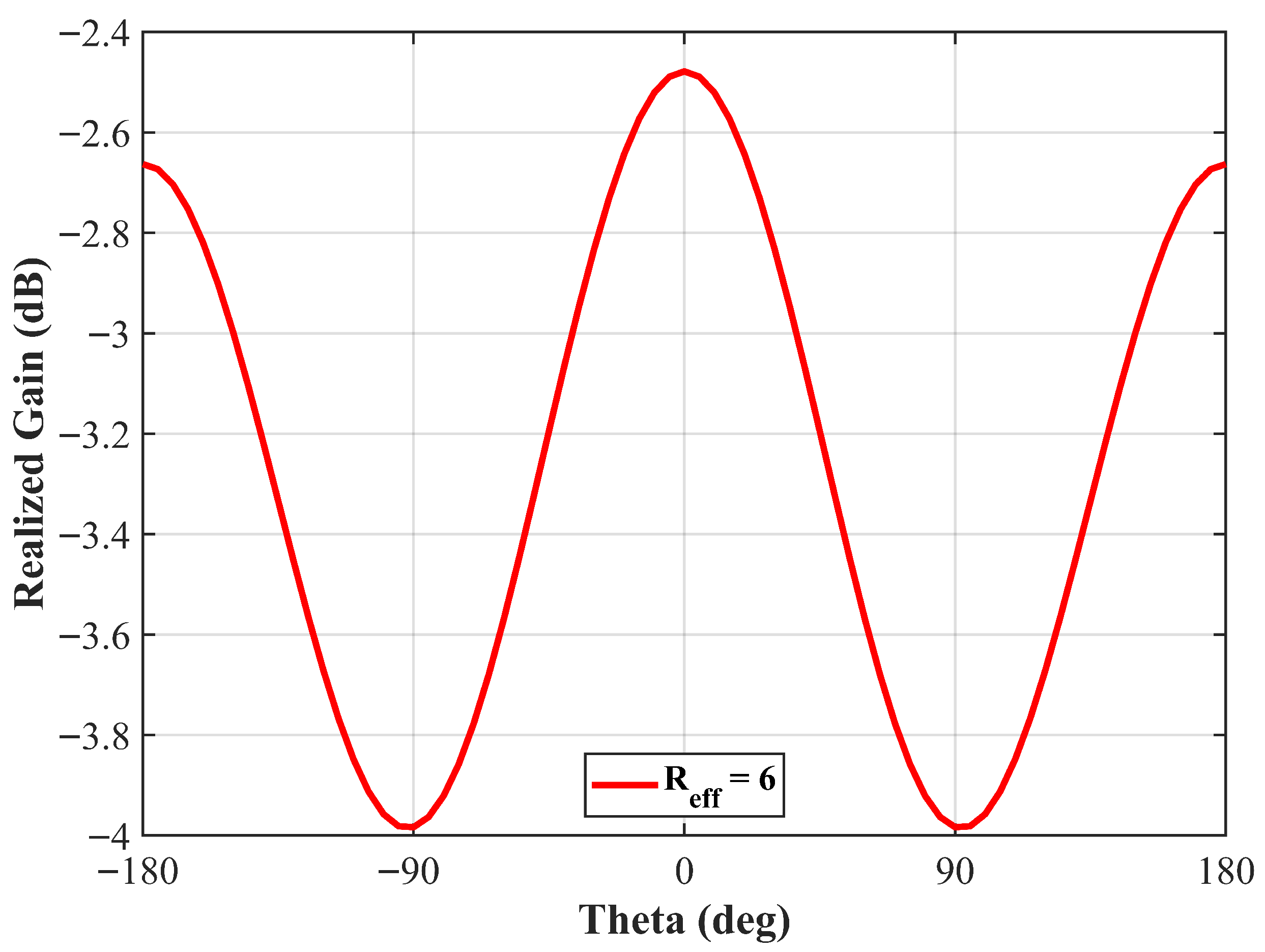
is also presented in
Figure 7. The realized gain of approximately
dBi is consistent with the experimentally measured value.
These results demonstrate that the measured antenna performance is a direct consequence of the expected electromagnetic behavior of highly transparent metallic mesh structures.
5. Optical Transparency Analysis
The sparse metallic mesh structure of the antenna provides transparency. The geometric aperture ratio of the grid structure can be used to theoretically estimate the effective optical transmittance (
) of the antenna region due to the high transparency of the polyimide substrate. The transparency of a square mesh lattice is defined as follows [
5]:
where
w is the width of the printed conductive lines and
p is the pitch (unit cell periodicity), defined as the sum of the line width and the spacing between lines (
).
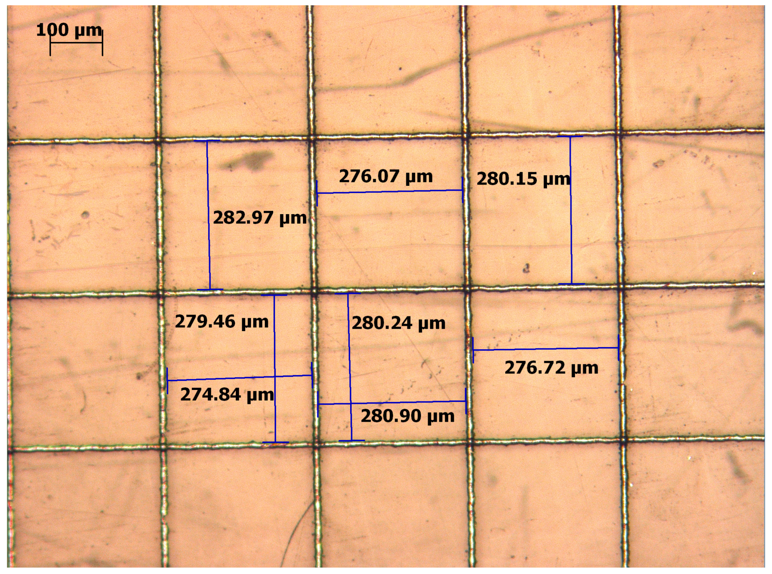
Optical microscopy was used to measure the geometric dimensions of the printed mesh and verify the fabrication precision (
Figure 8). The inter-line spacing (
s) and the average conductor width (
w) were found to be 279 μm and approximately 21 μm, respectively. This corresponds to a periodicity (
p) of 300 μm. From Equation (
2), the geometric optical transmittance was calculated as 86.5% using the measured dimensions. In order to validate the theoretical estimation, optical transmittance was also measured at a wavelength of 550 nm. The result was found to be approximately 85%, which shows excellent agreement with the theoretical calculation.
6. Integration with Photovoltaic Solar Cells
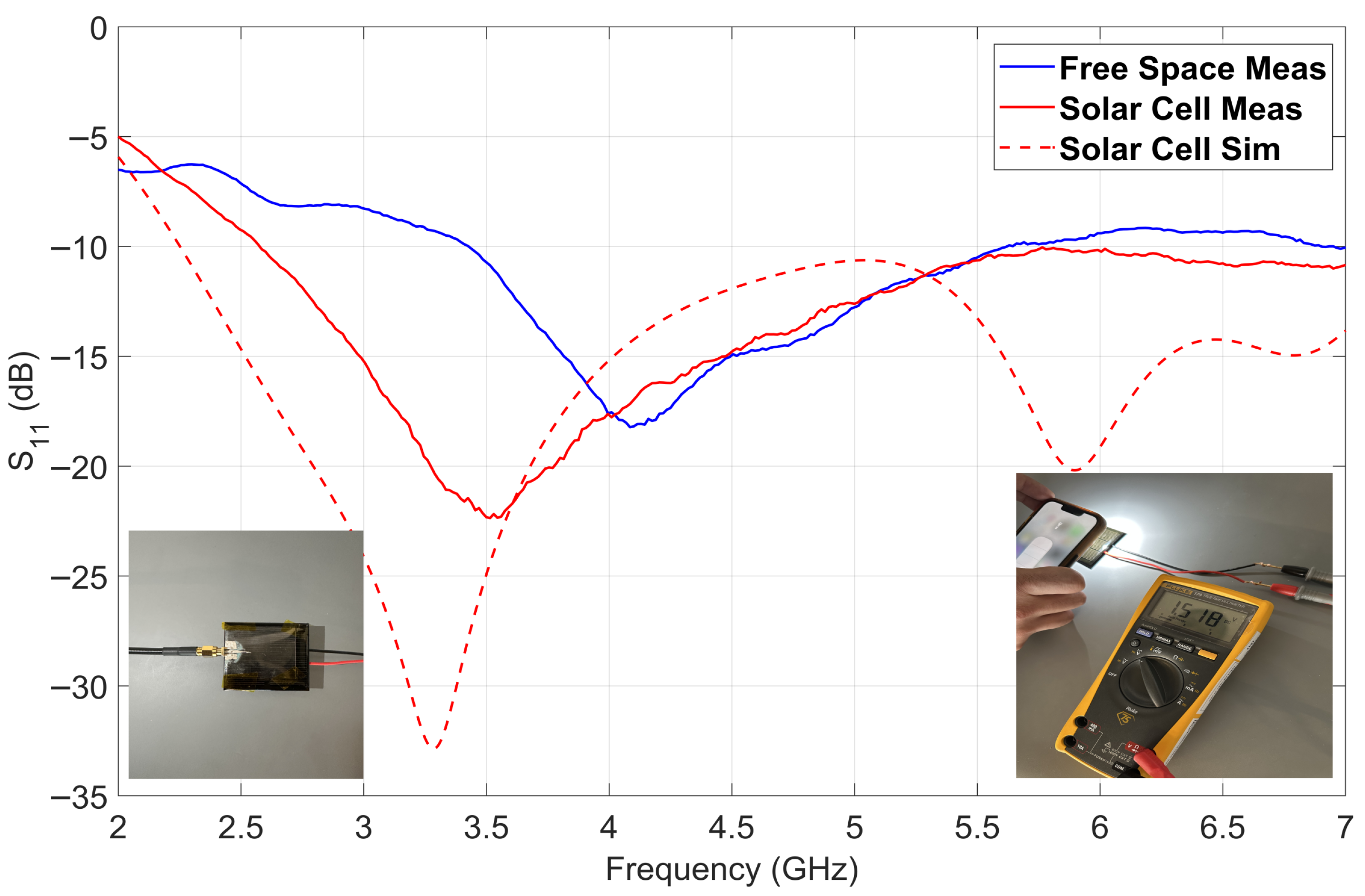
To understand the integration effects on the return loss, a test with a commercial solar cell was performed and the results are shown in
Figure 9. As seen from the results, this integration caused an approximately 600 MHz downward frequency shift. The encapsulation layer of the solar cell and the silicon layers inside result in such a shift. The antenna operates within the 3–6 GHz range, despite this expected change.
Furthermore, the effect of the antenna on the energy harvesting efficiency of the solar cell was also investigated. The solar cell open-circuit voltage () was approximately 1.5 V under ambient sunlight. It was observed that this voltage remained virtually unchanged when the antenna was placed over the cell. This result confirms that the metallic mesh structure has high optical transmittance and the solar cell continues to maintain its power generation under negligible shadowing conditions.
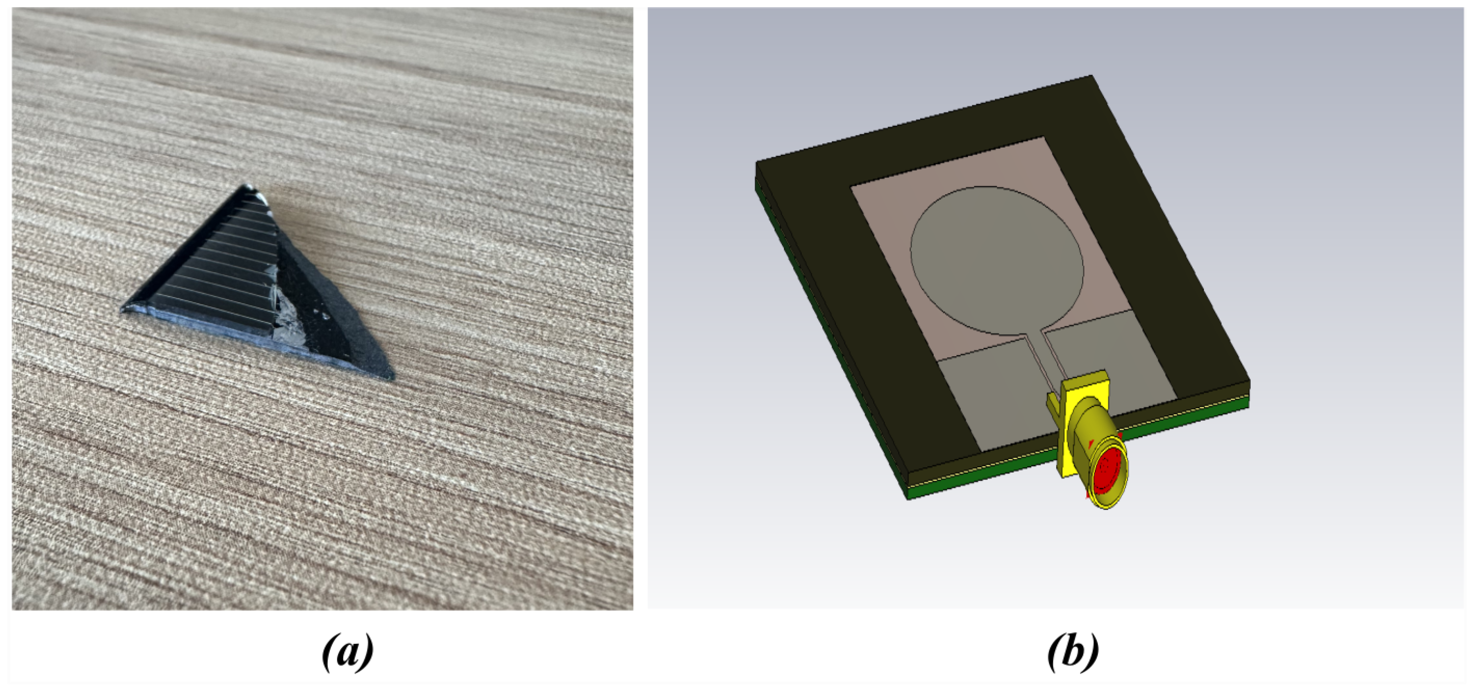
The commercial solar cell used in the experiments had dimensions of approximately 52 mm × 52 mm. To estimate its internal structure, the cell was examined by inspecting a fractured sample, as shown in
Figure 10a. Due to the lack of detailed information from the manufacturer regarding the commercial solar cell, a simplified dielectric multilayer model was used following common methods in the literature [
23,
24,
25]. A typical layered structure was assumed for the PV cell, comprising an epoxy encapsulation layer that was approximately 1.2 mm thick, a 0.2 mm-thick silicon layer, and a 1.5 mm FR-4 substrate layer, as depicted in
Figure 10b.
The resonance frequency shifting was found to be 900 MHz in the simulation. This is consistent with the ∼600 MHz frequency shift observed in the experiments, indicating that the detuning is mainly caused by the dielectric loading introduced by the PV cell layers.
7. Mechanical Flexibility and Performance on Curved Surfaces
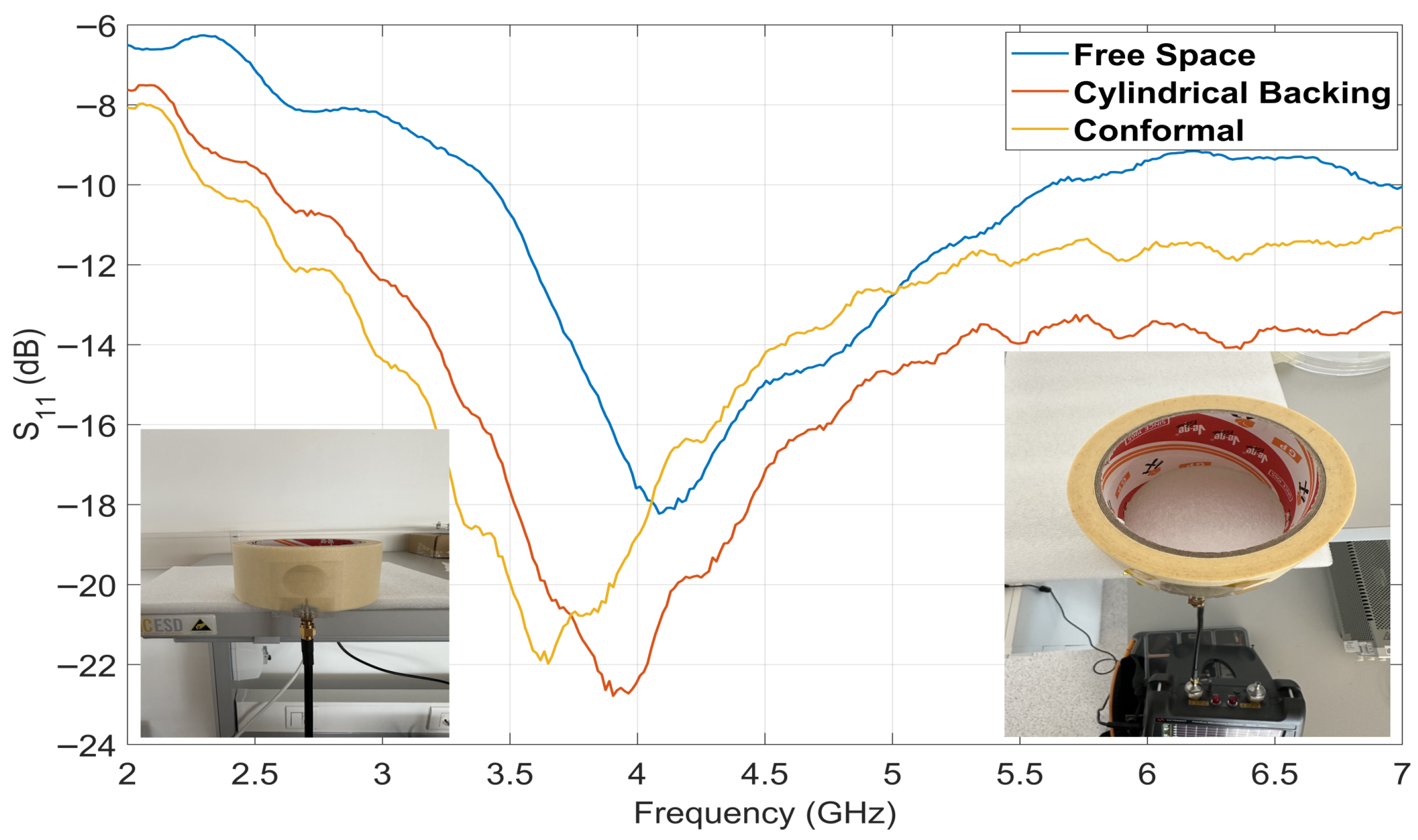
To demonstrate how the antenna can easily be mounted on different surfaces without mechanical degradation, the reflection coefficient was measured when mounted on a cylindrical body with a radius of 40 mm (
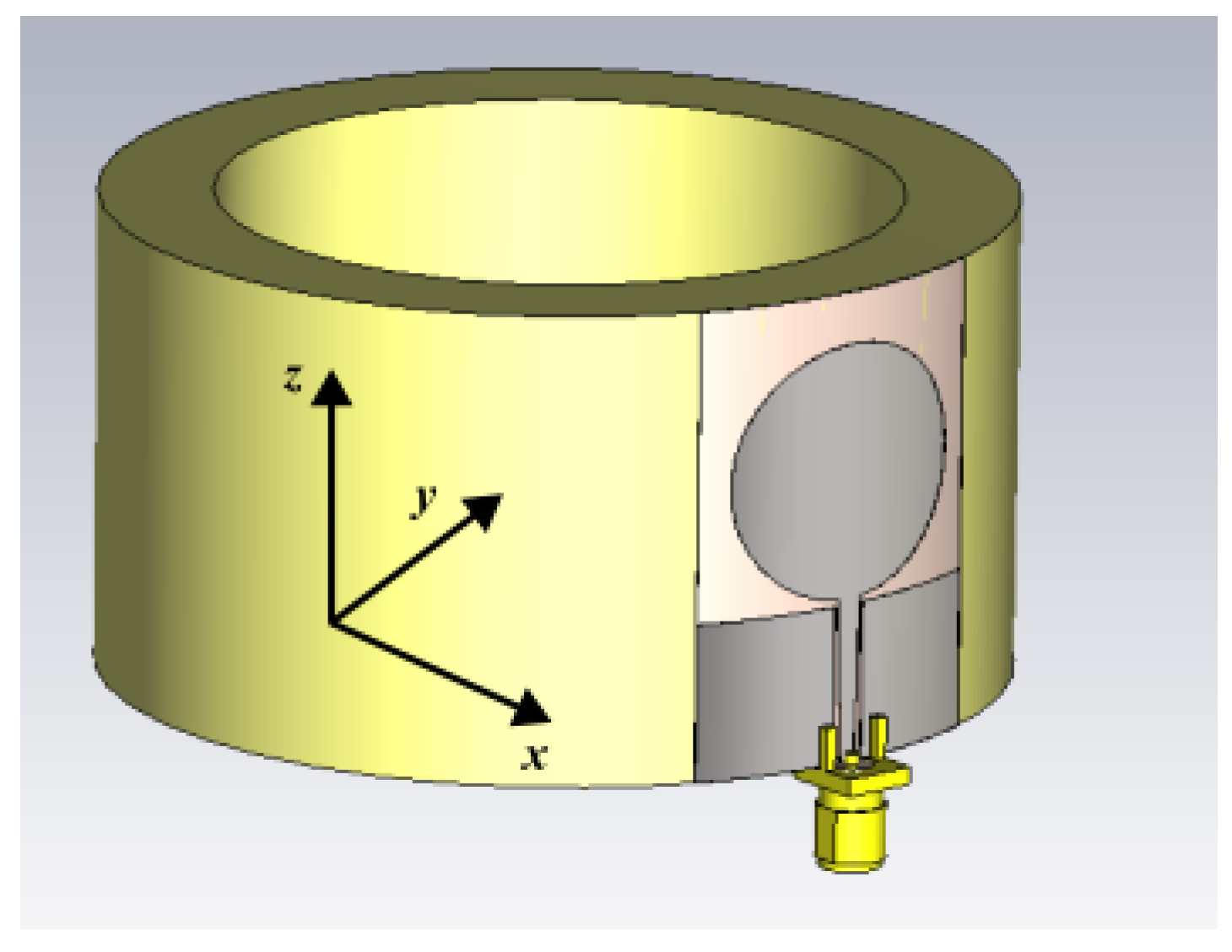
Figure 11). The corresponding simulation model, illustrating the antenna conformally mounted on the cylindrical surface, is depicted in
Figure 12. The radius of curvature varies according to the application requirements, so the antenna was wrapped around a cylindrical masking tape roll for practical demonstrations of its conformal characteristics.
In addition to the resonance shift due to backing on a cylindrical surface, which alters the effective dielectric constant (), an additional downward frequency shift was observed when the antenna was conformally bent. This additional downward frequency shift arises as a result of the increase in the effective electrical length of the antenna when it is bent around a curved surface. However, the antenna continues to exhibit good impedance matching characteristics over a wide bandwidth.
The resonance frequency of a monopole antenna can be approximately expressed as , where is the effective electrical length and is the effective dielectric constant. When the antenna is bent around a cylindrical surface, the current path along the radiating element becomes slightly longer due to the curved geometry, resulting in an increase in the effective electrical length. Furthermore, bending modifies the electromagnetic field distribution and enhances the interaction with nearby dielectric materials, thereby affecting . These combined effects lead to a shift in the resonance frequency toward lower values, which is consistent with the observed detuning behavior.
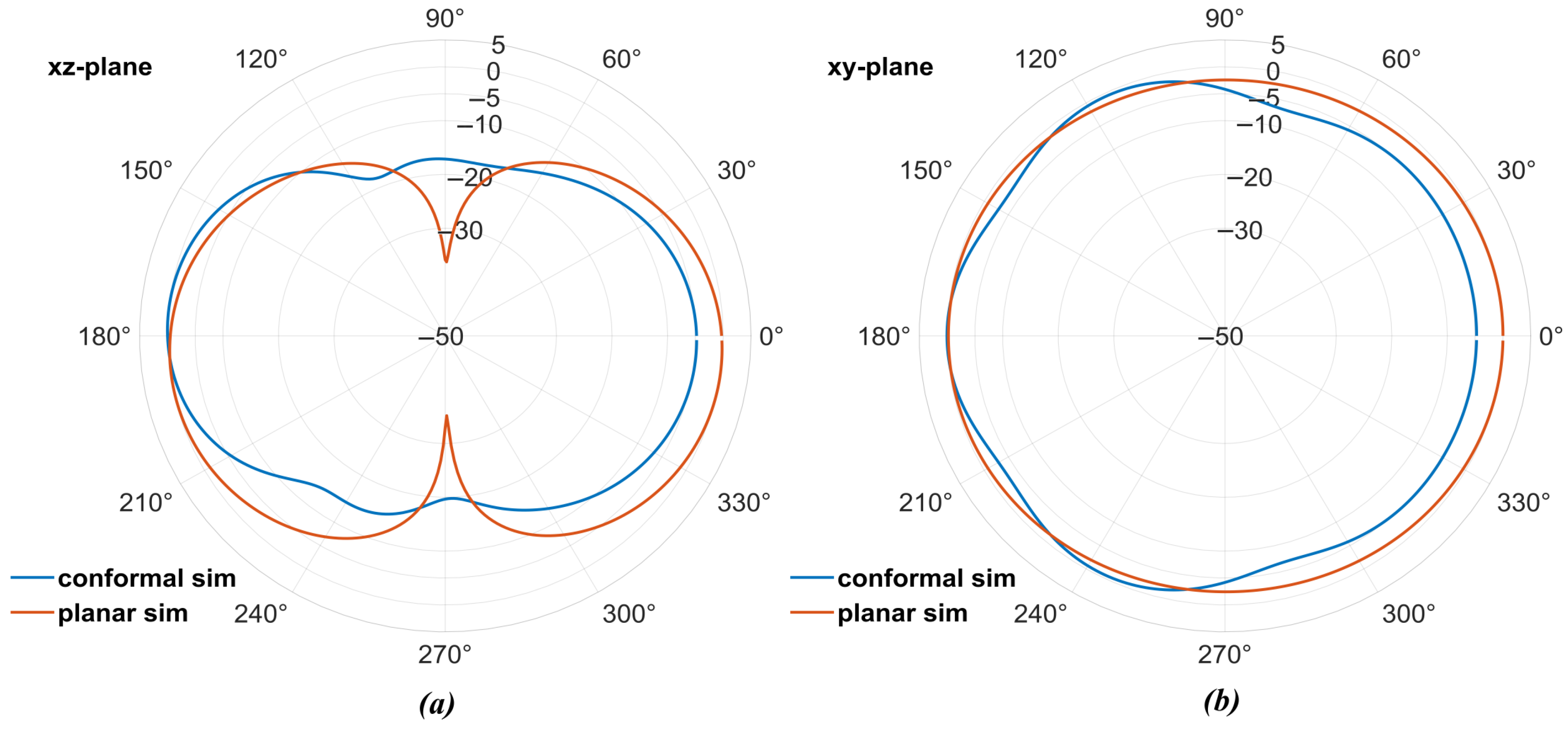
As shown in
Figure 13, the antenna maintains a similar radiation behavior after bending. In the
-plane (
Figure 13a), the radiation pattern exhibits noticeable changes in the null regions, with reduced null depths and a smoother overall radiation pattern. Similar effects have been reported for cylindrical conformal antennas in the literature [
26]. This behavior is mainly associated with the curvature-induced redistribution of the surface current and the modified electromagnetic interaction with the cylindrical support. In contrast, in the
-plane (
Figure 13b), the radiation pattern remains nearly omnidirectional, with only minor variations in the radiation levels.
8. Comparison of the Proposed Antenna with Reported Transparent Antennas
A comparison between recent studies and our work is presented in
Table 2. In addition to the realized gain comparison, the radiation efficiency values reported in the literature are included to provide a more comprehensive comparison with previously reported transparent antennas. As expected, antennas with higher optical transparency often exhibit reduced radiation efficiency owing to increased ohmic losses in the conductive mesh structures. Transparent antennas reported in the literature are mostly designed using Transparent Conductive Oxides (TCOs) or metal meshes/nanowires, each exhibiting distinct advantages and disadvantages.
For instance, antennas utilizing TCO materials, such as AgHT-4 or AgHT-8 [
10,
27], can provide wide impedance bandwidths; however, they usually have low optical transparency (less than 75%) and a brownish tinge due to their material properties. Although ITO-based designs can be more transparent, they often require hard glass substrates, making them unsuitable for conformal and wearable applications [
13].
In contrast, recent studies [
14,
28] have demonstrated that metal mesh and nanowire-based antennas yield superior optical transparency (>83%) and efficiency. However, due to their resonant characteristics, these designs often exhibit relatively narrow bandwidths (e.g., 4.4–5.0 GHz), unlike the broad bandwidth (3–6 GHz) achieved in this work. Furthermore, other flexible approaches fabricated with silver wires [
6] and conductive inks [
9] have been reported to suffer from lower realized gain and single-resonant-frequency operation.
The antenna described in [
13] achieves a higher gain than the original reference configuration after a number of geometric modifications in the design phase. The initial reference configuration was constructed as a single monopole element, and it resulted in negative gain. The addition of meandered feed lines and fractal elements to the initial reference design led to an increase in gain by enabling multiple current paths and improving the radiation characteristics. In contrast, the proposed antenna uses a circular monopole structure that provides good wideband performance, mechanical flexibility, and high optical transmittance. Therefore, a slightly lower realized gain is expected compared to geometrically complex designs specifically optimized for gain enhancement. Furthermore, while the referenced antenna is implemented on a rigid substrate, the proposed antenna maintains high performance under conformal bending conditions, making it more suitable for non-planar IoT and space applications.
The proposed antenna provides a balanced trade-off between optical transparency, bandwidth, and radiation characteristics. Although the realized gain of dBi is lower than that of fully metallic or non-transparent counterparts, it remains sufficient for short-range wireless communication scenarios, including IoT and indoor smart-surface applications. This trade-off arises from the simultaneous realization of wideband operation (3–6 GHz) and high optical transmittance, which remains a key challenge in the literature. Additionally, the antenna exhibits minimal shadowing when integrated with commercially available solar cells and can therefore be considered a promising candidate for conformal, energy-autonomous IoT systems.
9. Conclusions
The measurement and simulation results demonstrate that the proposed antenna operates within the 3–6 GHz frequency band. The printed mesh layer, which provides approximately 85% optical transparency and a realized gain of dBi, reflects the inherent trade-off between RF performance and optical transparency.
The impedance characteristics of the antenna are preserved under conformal bending and when placed over a commercial solar cell. The simulation results indicate that the observed frequency shifts are mainly caused by the dielectric properties of the PV layers and do not significantly affect the energy harvesting performance.
The study highlights the fundamental trade-off between transparency and conductivity in metallic mesh structures, which inherently limits the achievable antenna performance.
Because silver is susceptible to environmental degradation, protective coatings may be required for practical applications. However, because such coatings are located in the near-field region, they can affect impedance matching and return-loss characteristics. Therefore, antenna parameters should be re-optimized, and dielectric losses should be carefully considered when such layers are introduced.
The reported 85% optical transparency represents the maximum value under normal incidence conditions. In practical applications, particularly when the antenna is conformed to curved surfaces or viewed from different angles, a reduction in apparent transparency is expected. This effect is mainly caused by geometric shadowing, in which the physical thickness of the metallic mesh traces reduces the effective aperture area as the viewing angle deviates from the norm. Consequently, the visual clarity of the antenna depends on both the observation angle and the geometry of the supporting surface.
Although the achievable gain is limited by the transparency–conductivity trade-off, the use of parasitic elements or array configurations may enable improved radiation performance without significantly affecting transparency.
In conclusion, the proposed antenna provides a viable solution for “invisible” wireless communication systems, including smart surfaces, autonomous platforms, and CubeSat applications, demonstrating that transparency, flexibility, and reliable RF performance can be effectively combined within a single design.
Author Contributions
Conceptualization, M.O. and Y.S.A.; methodology, M.O. and Y.S.A.; software, M.O.; validation, M.O. and Y.S.A.; formal analysis, Y.S.A.; investigation, M.O.; resources, Y.S.A.; data curation, M.O. and Y.S.A.; writing—original draft preparation, M.O.; writing—review and editing, Y.S.A.; visualization, M.O.; supervision, Y.S.A.; project administration, Y.S.A.; funding acquisition, Y.S.A. All authors have read and agreed to the published version of the manuscript.
Funding
This research was supported by the Directorate of the Presidential Strategy and Budget of Turkey with Project No. 2019K12-149045.
Data Availability Statement
The data supporting the findings of this study are available from the corresponding author upon reasonable request.
Acknowledgments
The authors would like to thank Süleyman Özçelik and Berk Serbest, Director of the Gazi University Photonics Application and Research Center, for their contributions to the fabrication process and technical support with the Aerosol Jet® 5X printer.
Conflicts of Interest
The authors declare no conflicts of interest.
References
- Al-Fuqaha, A.; Guizani, M.; Mohammadi, M.; Aledhari, M.; Ayyash, M. Internet of Things: A Survey on Enabling Technologies, Protocols, and Applications. IEEE Commun. Surv. Tutor. 2015, 17, 2347–2376. [Google Scholar] [CrossRef]
- Hong, W. Solving the 5G Mobile Antenna Puzzle: Assessing Future Directions for the 5G Mobile Antenna Paradigm Shift. IEEE Microw. Mag. 2017, 18, 86–102. [Google Scholar] [CrossRef]
- Syed Feroze Hussain, S.; Thiripurasundari, D. A Review on Optically Transparent Antenna Fabricated with Conductive Nano-Material Oxides. J. Electron. Mater. 2022, 51, 6707–6734. [Google Scholar] [CrossRef]
- Dominguez, B.; Silva, F.; Baghel, A.; Albuquerque, D.; Pinho, P. Optically Transparent Antennas for 5G and Beyond: A Review. Electronics 2025, 14, 1616. [Google Scholar] [CrossRef]
- Silva, Z.J.; Valenta, C.R.; Durgin, G.D. Optically Transparent Antennas: A Survey of Transparent Microwave Conductor Performance and Applications. IEEE Antennas Propag. Mag. 2021, 63, 27–39. [Google Scholar] [CrossRef]
- Pan, J.; Yao, Y.; Yang, L.; Li, H.; He, S. Optically Transparent and Mechanically Flexible Coplanar Waveguide-fed Wideband Antenna Based on Sub-micron Thick Micro-metallic Meshes. Prog. Electromagn. Res. 2023, 176, 11–23. [Google Scholar] [CrossRef]
- Goliya, Y.; Rivadeneyra, A.; Salmeron, J.F.; Albrecht, A.; Mock, J.; Haider, M.; Russer, J.; Cruz, B.; Eschlwech, P.; Biebl, E.; et al. Next Generation Antennas Based on Screen-Printed and Transparent Silver Nanowire Films. Adv. Opt. Mater. 2019, 7, 1900995. [Google Scholar] [CrossRef]
- Zavanelli, N.; Yeo, W.H. Advances in Screen Printing of Conductive Nanomaterials for Stretchable Electronics. ACS Omega 2021, 6, 9344–9351. [Google Scholar] [CrossRef] [PubMed]
- Li, P.; Fleischer, J.; Quinn, E.; Park, D. Fabrication of an Optically Transparent Planar Inverted-F Antenna Using PEDOT-Based Silver Nanowire Clear Ink with Aerosol-Jet Printing Method towards Effective Antennas. J. Manuf. Mater. Process. 2024, 8, 39. [Google Scholar] [CrossRef]
- Hakimi, S.; Rahim, S.K.A.; Abedian, M.; Noghabaei, S.M.; Khalily, M. CPW-Fed Transparent Antenna for Extended Ultrawideband Applications. IEEE Antennas Wirel. Propag. Lett. 2014, 13, 1251–1254. [Google Scholar] [CrossRef]
- Desai, A.; Palandoken, M.; Elfergani, I.; Akdag, I.; Zebiri, C.; Bastos, J.; Rodriguez, J.; Abd-Alhameed, R.A. Transparent 2-Element 5G MIMO Antenna for Sub-6 GHz Applications. Electronics 2022, 11, 251. [Google Scholar] [CrossRef]
- Patil, E.C.; Lokhande, S.D. Optically transparent wideband circularly polarized antenna for 5G communication systems. Discov. Electron. 2025, 2, 64. [Google Scholar] [CrossRef]
- Jyothi, D.S.; Kumar, J. ITO-PET-based optically transparent circularly polarized fractal wideband antenna for 5G sub-6 GHz band. Sens. Actuators A Phys. 2025, 393, 116804. [Google Scholar] [CrossRef]
- Abbasi, M.N.; Aziz, A.; AlJaloud, K.; Chishti, A.R.; Alqahtani, A.H.; Abbasi, D.; Tahir, F.A.; Khan, Z.U.; Hussain, R. Design and optimization of a transparent and flexible MIMO antenna for compact IoT and 5G application. Sci. Rep. 2023, 13, 20620. [Google Scholar] [CrossRef] [PubMed]
- Nguyen, T.D.; Lee, Y.; Jung, C.W. Transparent and Flexible Patch Antenna Using MMF for Conformal WiFi-6E Applications. J. Electromagn. Eng. Sci 2023, 23, 310–317. [Google Scholar] [CrossRef]
- Kim, J.W.; Oh, J.I.; Kim, K.S.; Yu, J.W.; Jung, K.J.; Cho, I.N. Efficiency-Improved UWB Transparent Antennas Using ITO/Ag/ITO Multilayer Electrode Films. IEEE Access 2021, 9, 165385–165393. [Google Scholar] [CrossRef]
- John, D.M.; Vincent, S.; Pathan, S.; Kumar, P.; Ali, T. Flexible Antennas for a Sub-6 GHz 5G Band: A Comprehensive Review. Sensors 2022, 22, 7615. [Google Scholar] [CrossRef]
- Chishti, A.R.; Aziz, A.; Qureshi, M.A.; Abbasi, M.N.; Algarni, A.M.; Zerguine, A.; Hussain, N.; Hussain, R. Optically Transparent Antennas: A Review of the State-of-the-Art, Innovative Solutions and Future Trends. Appl. Sci. 2023, 13, 210. [Google Scholar] [CrossRef]
- Jepiti, P.; Kim, J.; Bark, S.; Lim, S. Transparent and printed RF electronics: A comprehensive review of materials, and applications. Mater. Des. 2025, 258, 114583. [Google Scholar] [CrossRef]
- Liang, J.; Chiau, C.; Chen, X.; Parini, C. Study of a printed circular disc monopole antenna for UWB systems. IEEE Trans. Antennas Propag. 2005, 53, 3500–3504. [Google Scholar] [CrossRef]
- Wang, X.R.; Wang, X.B.; Ren, H.; Wu, N.S.; Wu, J.W.; Su, W.M.; Han, Y.L.; Xu, S. Optically Transparent Microwave Shielding Hybrid Film Composited by Metal Mesh and Graphene. Prog. Electromagn. Res. 2021, 170, 187–197. [Google Scholar] [CrossRef]
- Albrecht, A.; Rivadeneyra, A.; Abdellah, A.; Lugli, P.; Salmerón, J.F. Inkjet printing and photonic sintering of silver and copper oxide nanoparticles for ultra-low-cost conductive patterns. J. Mater. Chem. C 2016, 4, 3546–3554. [Google Scholar] [CrossRef]
- Peter, T.; Rahman, T.A.; Cheung, S.W.; Nilavalan, R.; Abutarboush, H.F.; Vilches, A. A Novel Transparent UWB Antenna for Photovoltaic Solar Panel Integration and RF Energy Harvesting. IEEE Trans. Antennas Propag. 2014, 62, 1844–1853. [Google Scholar] [CrossRef]
- Shynu, S.V.; Roo Ons, M.J.; McEvoy, P.; Ammann, M.J.; McCormack, S.J.; Norton, B. Integration of Microstrip Patch Antenna with Polycrystalline Silicon Solar Cell. IEEE Trans. Antennas Propag. 2009, 57, 3969–3972. [Google Scholar] [CrossRef]
- Turpin, T.W.; Baktur, R. Meshed Patch Antennas Integrated on Solar Cells. IEEE Antennas Wirel. Propag. Lett. 2009, 8, 693–696. [Google Scholar] [CrossRef]
- Khan, T.A.; Khattak, M.I.; Asif, M.; Ahmad, G.; Ibrar, M.; Ali, E.M.; Alibakhshikenari, M.; Dalarsson, M. Radiation pattern synthesis in conformal antenna arrays using modified convex optimization technique. Int. J. RF Microw. Comput.-Aided Eng. 2022, 32, e23393. [Google Scholar] [CrossRef]
- Desai, A.; Palandoken, M.; Kulkarni, J.; Byun, G.; Nguyen, T.K. Wideband Flexible/Transparent Connected-Ground MIMO Antennas for Sub-6 GHz 5G and WLAN Applications. IEEE Access 2021, 9, 147003–147015. [Google Scholar] [CrossRef]
- Qiu, H.; Liu, H.; Jia, X.; Jiang, Z.Y.; Liu, Y.H.; Xu, J.; Lu, T.; Shao, M.; Ren, T.L.; Chen, K.J. Compact, Flexible, and Transparent Antennas Based on Embedded Metallic Mesh for Wearable Devices in 5G Wireless Network. IEEE Trans. Antennas Propag. 2021, 69, 1864–1873. [Google Scholar] [CrossRef]
Figure 1.
Geometry of the proposed antenna (a) top view; (b) side view.
Figure 1.
Geometry of the proposed antenna (a) top view; (b) side view.
Figure 2.
(a) Aerosol Jet® 5X printing machine; (b) Fabricated antenna.
Figure 2.
(a) Aerosol Jet® 5X printing machine; (b) Fabricated antenna.
Figure 3.
Measurement setup inside the anechoic chamber.
Figure 3.
Measurement setup inside the anechoic chamber.
Figure 4.
Measured and simulated results of the antenna reflection coefficient.
Figure 4.
Measured and simulated results of the antenna reflection coefficient.
Figure 5.
Measured and simulated co-polarized radiation patterns of the antenna at 4.5 GHz: (a) xz-plane; (b) xy-plane.
Figure 5.
Measured and simulated co-polarized radiation patterns of the antenna at 4.5 GHz: (a) xz-plane; (b) xy-plane.
Figure 6.
Simulated total efficiency versus frequency for different effective sheet resistance values .
Figure 6.
Simulated total efficiency versus frequency for different effective sheet resistance values .
Figure 7.
Simulated realized gain pattern for .
Figure 7.
Simulated realized gain pattern for .
Figure 8.
Microscopic view of the printed metallic mesh and measured dimensions.
Figure 8.
Microscopic view of the printed metallic mesh and measured dimensions.
Figure 9.
Measurement setup for the transparent antenna integrated with a photovoltaic solar cell, and measured/simulated reflection coefficient () comparing the free-space and solar-cell-integrated configurations.
Figure 9.
Measurement setup for the transparent antenna integrated with a photovoltaic solar cell, and measured/simulated reflection coefficient () comparing the free-space and solar-cell-integrated configurations.
Figure 10.
Integration of the proposed antenna with the photovoltaic solar cell: (a) fractured solar cell sample used to inspect the approximate internal layer structure; (b) simulation model of the antenna placed on the solar cell (black: epoxy; yellow: silicon; green: FR-4 substrate).
Figure 10.
Integration of the proposed antenna with the photovoltaic solar cell: (a) fractured solar cell sample used to inspect the approximate internal layer structure; (b) simulation model of the antenna placed on the solar cell (black: epoxy; yellow: silicon; green: FR-4 substrate).
Figure 11.
Measurement setup of the conformal antenna under bending conditions on a cylindrical support, and measured reflection coefficient () for free-space, cylindrical backing, and conformal bending configurations.
Figure 11.
Measurement setup of the conformal antenna under bending conditions on a cylindrical support, and measured reflection coefficient () for free-space, cylindrical backing, and conformal bending configurations.
Figure 12.
Simulation model of the proposed antenna conformally mounted on a cylindrical surface (radius = 40 mm) with the corresponding coordinate system.
Figure 12.
Simulation model of the proposed antenna conformally mounted on a cylindrical surface (radius = 40 mm) with the corresponding coordinate system.
Figure 13.
Comparison of the simulated radiation patterns of the planar and conformal antenna configurations in the (a) xz-plane and (b) xy-plane.
Figure 13.
Comparison of the simulated radiation patterns of the planar and conformal antenna configurations in the (a) xz-plane and (b) xy-plane.
Table 1.
Design parameters of the proposed antenna.
Table 1.
Design parameters of the proposed antenna.
| Parameter | Dimension (mm) |
|---|
| 30.00 |
| 45.00 |
| h | 0.05 |
| r | 12.50 |
| g | 0.20 |
| 2.20 |
| 1.60 |
| 13.50 |
Table 2.
Comparison of the proposed antenna with recently reported antennas.
Table 2.
Comparison of the proposed antenna with recently reported antennas.
| Reference | Frequency (GHz) | Conductor Type/Structure | O.T. (%) | Peak Gain (dBi) | Flexibility | Efficiency (%) |
|---|
| This study | 3–6 | Aerosol Jet® 5X (Metal Mesh) | 85% | −2.5 | High | 30 |
| [6] | 2.45 | Ag NWs/Screen Printing | 85% | N/A | Yes | 89.7 |
| [9] | 2.45 | PEDOT:PSS/Aerosol Jet | ∼80% | −3.6 | Limited | 10 |
| [10] | 3.15–32 | AgHT-8/Laser Cutting | >75% | −4.8 (Avg) | Yes | – |
| [13] | 2.99–6.82 | ITO-PET/Manual Cutting | <87% | 1.3 | No | 40–68 |
| [14] | 4.41–4.56 | Wired Metal Mesh | 83% | 3.2 | Yes | 61 |
| [27] | 2.21–6 | AgHT-4/Manual Cutting | 70% | 0.53 | Yes | 41 |
| [28] | 4.4–5 | Ni-Metallic Mesh/Electrodeposition | 91% | 3.8 | Yes | 78–85 |
| Disclaimer/Publisher’s Note: The statements, opinions and data contained in all publications are solely those of the individual author(s) and contributor(s) and not of MDPI and/or the editor(s). MDPI and/or the editor(s) disclaim responsibility for any injury to people or property resulting from any ideas, methods, instructions or products referred to in the content. |