Understanding the impedance characteristics of DDWTs is fundamental for analyzing their interactions with the grid and assessing the risk of sub/super-synchronous oscillations. Since the dominant oscillation mechanisms of DDWTs originate from the control dynamics of the full-scale power converter, particularly the grid-side converter (GSC), an accurate frequency domain impedance model is required to characterize the converter response to grid disturbances under different operating conditions. Therefore, a detailed impedance model is presented in this section.
2.1. Overall Structure and Control Architecture of a Distributed DDWT
A typical DDWT mainly consists of a wind turbine rotor, a drive shaft, a permanent magnet synchronous generator (PMSG), a machine-side converter (MSC), a dc link capacitor, a GSC, an ac filter, and the associated converter control system [
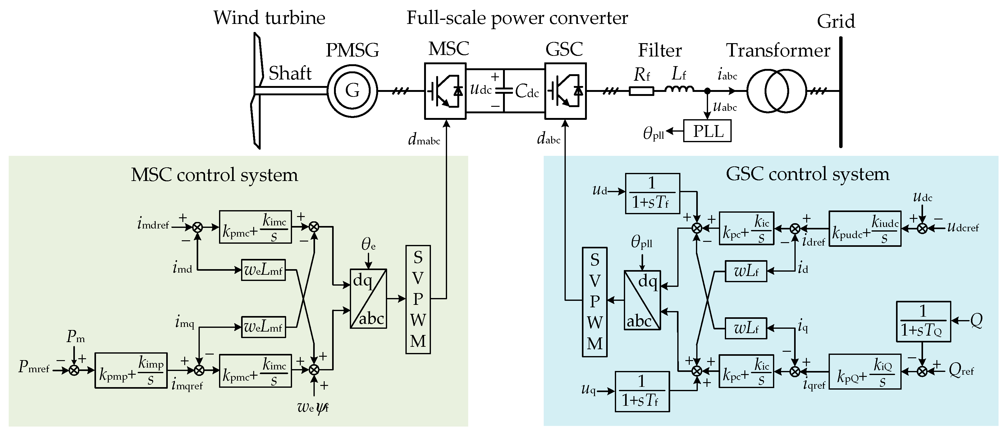
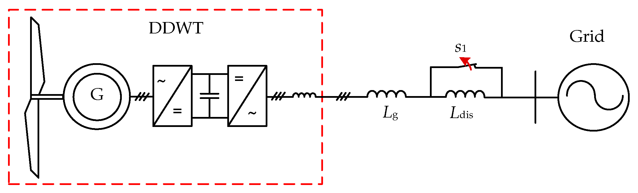
8]. The mechanical power captured by the wind turbine is directly transmitted to the PMSG without a gearbox, which enhances system reliability and reduce mechanical losses. The PMSG generates three-phase electrical power, which is rectified by the MSC into dc power. A dc link capacitor is employed to stabilize the intermediate dc link voltage. Subsequently, the GSC converts the dc power into ac power and injects it into the grid through a filter. The overall configuration of the distributed DDWT is illustrated in
Figure 1. In
Figure 1,
udc is the dc link voltage,
uabc is the three-phase terminal voltage of the DDWT,
iabc is the three-phase output current of the DDWT,
Cdc denotes the dc link capacitance, and
Rf and
Lf represent the resistance and inductance of the filter, respectively.
θe is the electrical angle of the PMSG, while
θpll is the phase angle of the PLL.
The MSC regulates the PMSG to extract maximum available wind power, typically adopting a dual-loop control structure consisting of an outer loop and an inner loop. The maximum power point tracking (MPPT) module calculates the optimal aerodynamic power and generates the corresponding active power reference Pmref, which serves as the reference for the outer loop. The outer power controller compares the MPPT power reference Pmref with the measured generator active power Pm. The resulting power error is processed by a PI controller to generate the q-axis current reference imqref, while the d-axis current reference imdref is typically set to zero to regulate the stator flux.
Accordingly, the current references (
imqref and
imdref) can be expressed as
where
kpmp and
kimp are the proportional and integral coefficients of the MSC active power outer loop, respectively.
The three-phase generator currents are transformed into the synchronous dq reference frame to obtain the current components
imd and
imq. The inner current control loop employs PI regulators with feedforward compensation to track the references
imdref and
imqref, and generates the corresponding dq-axis voltage references
umdref and
umqref, given by
where
kpmc and
kimc are the proportional and integral coefficients of the MSC current inner loop, respectively,
ωe is the electric angular speed of the generator,
Lmf is the filter inductance of MSC, and
Ψf is the stator flux linkage.
The voltage references umdref and umqref are transformed into the abc frame through inverse Park transformation. Subsequently, space vector pulse width modulation (SVPWM) is applied to generate the switching signals dmabc for the MSC semiconductor devices.
The GSC also adopts a dual-loop control structure consisting of the outer loops and inner loops. The outer loops include a dc link voltage control loop and a reactive power control loop. The dc link voltage loop regulates the dc link voltage and generates the d-axis current reference
idref, which governs the active power exchange between the converter and the grid. Meanwhile, the reactive power loop produces the q-axis current reference
iqref, enabling independent reactive power regulation. The current references can be expressed as
where
udcref is the dc link voltage reference, and
kpudc and
kiudc are the proportional and integral coefficients of the dc link voltage loop, respectively.
Qref is the reactive power reference.
kpQ and
kiQ are the proportional and integral coefficients of the reactive power loop, respectively.
Qf denotes the filtered reactive power obtained by passing the measured reactive power
Q through a first-order filter with the time constant
TfQ, which is described by
.
The three-phase currents
iabc are transformed into the synchronous dq reference frame using the phase angle estimated by the PLL, yielding the current components
id and
iq. These currents are compared with their references, and the resulting errors are processed by PI controllers with feedforward compensation to generate the dq-axis voltage references
ugdref and
ugqref, expressed as
where
kpc and
kic are the proportional and integral coefficients of the GSC current inner loop, respectively, and
ω is the grid angular frequency.
udf and
uqf denote the filtered voltage components in the dq frame obtained by passing the measured voltage components in the dq frame
ud and
uq through a first-order filter with the time constant
Tf, which is described by
,
.
The voltage references ugdref and ugqref are transformed into the abc frame through inverse Park transformation. SVPWM is then applied to generate the switching signals dabc for the GSC semiconductor devices. ud and uq are the grid voltage components in the dq frame, respectively.
2.2. Impedance Modeling of a DDWT
Following the modeling principles in [
28], the dq domain admittance of the DDWT
Ydq can be expressed as
where
where
s is the Laplace operator,
udcn is the rated dc-link voltage, and
Pg is the active power of the DDWT.
ud4s and
uq4s are the steady-state d- and q-axis voltage components at the side of the GSC under the electrical coordinates reference frame, while
id4s and
iq4s are the corresponding steady-state current components.
uid4s and
uiq4s are the steady-state d- and q-axis voltage components at the point of common coupling (PCC) under electrical coordinates reference frame.
Hc is the transfer function of the current inner loop PI controller, given by
Hc =
kpc +
kic/
s.
Hudc and
HQ are the transfer function of the dc link voltage loop and reactive power control loop, respectively, expressed as
Hudc =
kpudc +
kiudc/
s and
HQ =
kpQ +
kiQ/
s.
Hf is the voltage feedforward filter, expressed as
Hf = 1/(1 +
sTf), and
Tf is the filter time constant.
HfQ is the transfer function of the first-order filter of the reactive power control loop, expressed as
HfQ = 1/(1 +
sTfQ), and
TfQ is the filter time constant.
In Equation (14), the PLL-related transfer functions
Gupll,
Gipll, and
Guipll can be expressed as
where
where
Hpll is the transfer function of the PLL, which can be expressed as
Hpll =
kppll +
kipll/
s, and
kppll and
kipll are the proportional and integral coefficients of the PLL, respectively.
The resulting dq domain admittance
Ydq of the DDWT is 2 × 2 transfer matrix
To facilitate oscillation analysis in the sequence domain,
Ydq is further transformed into the positive sequence admittance
Yp using the standard transformation function [
25]
Subsequently, the corresponding sequence impedance
Zp can be obtained as
It should be noted that the dq-domain impedance model established above is derived based on the dq-transformation and small-signal linearization around a steady-state operating point. This modeling method assumes balanced three-phase conditions and sufficiently small perturbations, such that the system dynamics can be approximated as linear and time-invariant at each analyzed frequency. Under fast power variations or control saturation, these assumptions may be violated, potentially leading to reduced modeling accuracy. Such limitations are inherent to small-signal dq-domain impedance modeling and define its applicable analysis scope.
To verify the correctness of the established impedance model, a simulation model of the DDWT is established in PSCAD/EMTDC. The main parameters are listed in
Table 1. The PI control parameters of converter were selected based on standard bandwidth separation principles and typical industrial practice. Specifically, the current loop was designed with a bandwidth significantly higher than those of the dc-link voltage loop and the PLL. The outer loop control parameters were then tuned to achieve stable operation under the nominal operating condition.
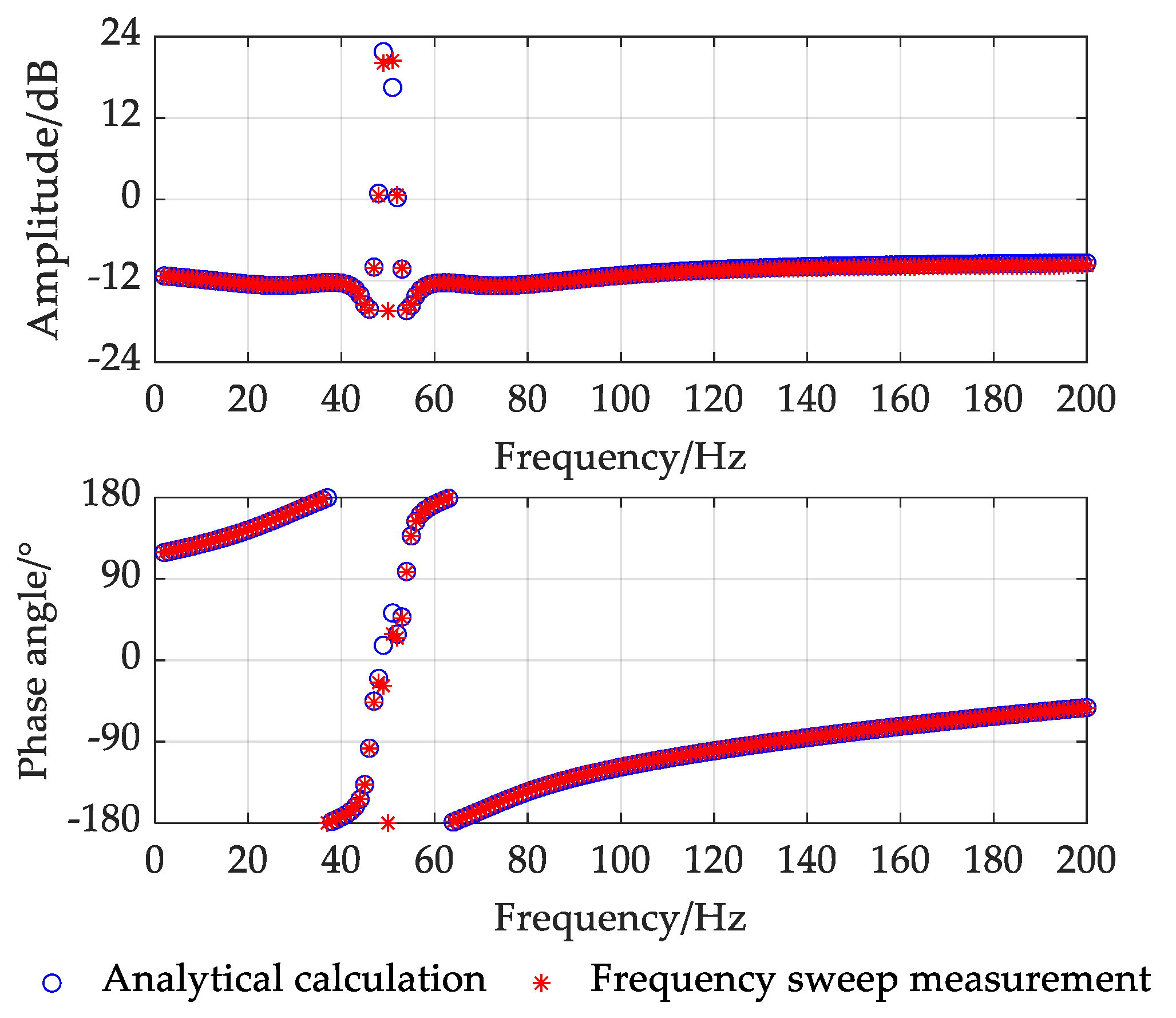
A small amplitude sinusoidal voltage perturbation is injected at the voltage source, and the resulting current response is recorded. The impedance frequency sweep is performed from 2 Hz to 200 Hz. The starting frequency of 2 Hz is selected in accordance with common impedance scanning practices [
29,
30] and is used solely for impedance model verification, without implying a theoretical lower bound of the applicability of the proposed method. The proposed impedance modeling and clustering method remains valid below 2 Hz. The upper limit of 200 Hz is chosen to capture the dominant control-induced dynamics for sub- and super-synchronous oscillations, including the effects of the PLL, the dc-link voltage loop, and the major portion of the current loop. In contrast, higher frequency oscillations associated with switching harmonics, PWM modulation, and filter are beyond the scope of this study. Specifically, the current loop bandwidth is typically on the order of several hundred hertz but below the switching frequency, while the bandwidths of the dc-link voltage loop and the PLL are generally on the order of several tens of hertz, making 200 Hz sufficient to capture the oscillatory phenomena of interest. Based on the measured voltage and current, the sequence impedance
Zp_sim is computed and compared with the analytically derived impedance
Zp, as shown in
Figure 2. Based on
Figure 2, excellent consistency is observed in both magnitude and phase across the entire frequency range, thereby validating the accuracy of the established impedance model.