Article

Integrated Analytical Design of Boost DC–DC Converters and Cascade Current-Mode Control Using Integer- and Fractional-Order Lead–Lag Compensators

by
Carlos Muñiz-Montero
1,
Gerardo Peña-López
2,
Esteban Tlelo-Cuautle
3,*,
Sandra Huerta-Moro
4,
Carlos Sánchez-López
5,
Juan A. Arizaga-Silva
6 and
Luis A. Sánchez-Gaspariano
4
1
Academic Program in Electronics and Telecommunications, Universidad Politécnica de Puebla, Juan C. Bonilla 72660, Puebla, Mexico
2
Doctoral Program in Engineering Sciences, Universidad Autónoma del Carmen, Ciudad del Carmen 24180, Campeche, Mexico
3
Department of Electronics, Instituto Nacional de Astrofísica, Óptica y Electrónica, Tonantzintla 72840, Puebla, Mexico
4
Faculty of Electronics Sciences, Benemérita Universidad Autónoma de Puebla (BUAP), Puebla 72570, Puebla, Mexico
5
Faculty of Basic Sciences, Engineering and Technology, Autonomous University of Tlaxcala, Apizaco 90300, Tlaxcala, Mexico
6
Academic Program in Automotive Systems, Universidad Politécnica de Puebla, Juan C. Bonilla 72660, Puebla, Mexico
*
Author to whom correspondence should be addressed.
Electronics 2026, 15(18), 4240; https://doi.org/10.3390/electronics15184240
Submission received: 25 July 2026 / Revised: 9 September 2026 / Accepted: 10 September 2026 / Published: 17 September 2026
(This article belongs to the Special Issue Feature Papers in Circuit and Signal Processing, 2nd Edition)

Abstract

This paper presents an integrated specification-driven analytical methodology for the design and practical implementation of cascade-controlled Boost DC–DC converters using integer-order and fractional-order lead–lag compensators. Unlike empirical tuning and optimization-based approaches, the proposed framework derives the controller parameters analytically from prescribed transient- and steady-state-performance requirements and, for the fractional-order lead–lag (FO–LL) controller, explicitly incorporates the control-effort level as an additional design specification. The methodology integrates converter sizing, averaged small-signal modeling, controller synthesis, rational approximation of fractional-order dynamics, electronic realization, and software-assisted verification within a reproducible workflow implemented in MATLAB, Simulink, and Simscape. The methodology is first evaluated using a numerical assessment case that examines sensitivity to the fractional approximation order, operation away from the nominal point, converter-parameter variations, controller-component tolerances, and load disturbances. Practical feasibility is then demonstrated using a separate experimental implementation case based on a second Boost converter with a hybrid IO–LL/FO–LL cascade configuration, evaluated through three validation levels—block-level simulation, switching circuit-level simulation, and experimental evaluation. The circuit-level and experimental evaluations exhibit consistent transient behavior under their respective test conditions, with representative overshoots of 5.02% and 4.2%, respectively, while the experimental prototype maintains a steady-state error of approximately 1% and achieves approximately 91% conversion efficiency. Overall, the results demonstrate that the proposed methodology provides a systematic and reproducible path from performance specifications to practical controller realization while retaining stable operation and implementation-oriented control effort under the evaluated modeling, operating, and hardware variations.

1. Introduction

The increasing use of renewable-energy systems, electric vehicles, battery-management systems, aerospace applications, and DC microgrids has intensified the demand for efficient and reliable DC–DC power converters. Depending on the required voltage-conversion ratio, these converters can be implemented using Buck, Boost, Buck–Boost, Cuk, Zeta, and Sepic topologies [1,2,3]. Among them, the Boost converter is particularly attractive when the required output voltage exceeds the available input voltage, as occurs in photovoltaic systems, fuel cells, battery-powered systems, DC microgrids, and electric transportation. Boost converters are also employed as PFC stages in wireless electric-vehicle charging systems, where power losses and conversion efficiency can have important thermal implications [4].
A DC–DC converter comprises passive energy-storage elements, semiconductor switching devices, and a feedback-control system [1,2]. Although a single voltage loop can be used for output regulation, high-performance applications frequently employ cascade architectures consisting of a fast inner current loop and a slower outer voltage loop. Such voltage–current cascade structures have also been experimentally implemented in Boost-derived converters to maintain output-voltage regulation under load variations [5]. This structure improves current regulation, output-voltage tracking, and disturbance rejection. Nevertheless, the integrated design of the power stage and its control system remains challenging because DC–DC converters are nonlinear switched systems subject to operating-point variations, parameter uncertainties, parasitic effects, and disturbances [1,2,3]. Consequently, the design must simultaneously consider transient performance, steady-state accuracy, robustness, control effort, and practical implementation constraints.
A wide variety of control strategies have been proposed for DC–DC converters, including PID controllers, frequency-domain compensators, sliding-mode control, active disturbance rejection control, and model predictive control [6,7,8,9,10]. PID controllers remain attractive because of their simplicity and ease of implementation [8], whereas phase lead–lag, PI–Lead, and Type-III compensators provide frequency-domain formulations that relate stability margins and crossover frequencies to controller parameters [7,11,12]. Other approaches, including sliding-mode control, active disturbance rejection control, and model predictive control, have also been applied to DC–DC converters to improve robustness and disturbance rejection [9,10,13]. These approaches involve different design elements, such as sliding surfaces, disturbance observers, prediction models, or optimization procedures, depending on the control strategy.
Fractional-order control extends conventional differentiation and integration operators to noninteger orders, providing additional degrees of freedom for shaping transient response, robustness, and disturbance rejection [14,15,16]. Its application to renewable-energy systems and power converters has consequently received increasing attention, including experimental and hardware-in-the-loop implementations [17,18,19]. Recent approaches have also combined fractional-order control with operating-point-dependent tuning and metaheuristic optimization. For example, Muñoz Hernandez et al. [20] applied a gain-scheduled FO-PID controller to a quadratic Buck converter, whereas Ghamari et al. [19] employed the Snake Optimization algorithm to tune an FOPID controller for a Buck–Boost converter. Nevertheless, controller synthesis and practical realization remain important challenges.
Table 1 summarizes representative methodologies reported for the control of DC–DC converters. The selected works include classical and fractional-order controllers, analytical and optimization-based design procedures, single-loop and cascade architectures, and simulation and experimental validation. The comparison is intended to identify how these characteristics have been combined in previous studies and to place the proposed methodology within this context.
Table 1 shows that analytical, fractional-order, cascade, and experimentally validated control strategies have been reported for DC–DC converters. However, these features are generally addressed from different perspectives rather than within a unified design framework. Analytical frequency-domain approaches derive controller parameters through explicit design relationships [7,11,12], whereas several fractional-order approaches rely on numerical search, optimization, operating-point-dependent gain scheduling, or additional tuning procedures [10,20,26,27,29]. Experimental realizations have also demonstrated the practical feasibility of different control strategies.
Nevertheless, comparatively limited attention has been devoted to integrated analytical frameworks that jointly address power-stage sizing, cascade-controller synthesis, fractional-order design, and practical realization. This observation defines the research gap addressed in this work: the need for a systematic methodology that connects the electrical specifications of the Boost converter with the synthesis and implementation of its cascade control system through a unified analytical design procedure.
To address this gap, this paper proposes an integrated methodology in which the Boost converter is first sized from its electrical specifications and the inner current and outer voltage controllers are subsequently synthesized from prescribed performance requirements. The controller synthesis builds on the analytical integer-order lead–lag design of Wang et al. [30] and its fractional-order extension proposed by Tavazoei et al. [31], which are incorporated here into a unified cascade-design framework. The performance requirements are mapped into frequency-domain quantities and then into controller parameters through explicit analytical relationships, avoiding optimization-based or trial-and-error tuning. In the fractional-order case, the additional degree of freedom is used to incorporate a prescribed initial control signal into the synthesis. The resulting controllers are finally translated into practical analog realizations, completing the design path from converter specifications to controller implementation.
The main contributions of this work can be summarized as follows:
  • An integrated analytical methodology for the design of the Boost power stage and its cascade control system from prescribed electrical and performance specifications.
  • Integration of integer-order and fractional-order phase lead–lag analytical design procedures into the synthesis of the inner current and outer voltage loops, avoiding optimization-based, heuristic, or trial-and-error controller tuning. In the fractional-order case, the additional degree of freedom is exploited to impose a constraint on the initial control effort.
  • A complete engineering workflow connecting converter sizing and controller synthesis with software automation, operational-amplifier realization, numerical and circuit-level simulation, and experimental validation of the hybrid IO–LL/FO–LL cascade configuration.
The remainder of this paper is organized as follows. Section 2 presents the theoretical background. Section 3 develops the proposed integrated analytical design methodology, including the electronic realization and software implementation. Section 4 presents the numerical simulation and robustness analyses. Section 5 presents the circuit-level and experimental validation. Section 6 discusses the main findings, their implications, and the scope and potential extension of the proposed methodology. Finally, Section 7 summarizes the main conclusions.

2. Theoretical Background

2.1. Fractional Calculus Fundamentals

Fractional calculus extends conventional integer-order calculus by allowing differentiation and integration operations of arbitrary real order. The fractional-order operator is denoted by D t q b , where b and t represent the operation limits and q ∈ R denotes the fractional order. For q > 0 , the Riemann–Liouville definition is given by [16,32]       
D t q b f ( t ) = 1 Γ ( m − q ) d d t m ∫ b t f ( τ ) ( t − τ ) q − m + 1 d τ ,
where m − 1 < q < m , m ∈ N , and Γ ( · ) is the Gamma function. For q > 0 , q < 0 , and q = 0 , the fractional operator represents fractional differentiation, fractional integration, and the identity operator, respectively. Under zero initial conditions, its Laplace transform can be expressed as [32]
L D t q b f ( t ) = s q F ( s ) ,
where F ( s ) = L { f ( t ) } and s is the Laplace variable. Evaluating the fractional power on the imaginary axis, s = j ω , gives
( j ω ) q = ω q cos q π 2 + j sin q π 2 .
Fractional differential equations can therefore be represented in the Laplace domain using transfer functions containing noninteger powers of s. Considering x ( t ) and y ( t ) as the input and output signals, respectively, a general fractional-order transfer function can be expressed as [33]
H ( s ) = Y ( s ) X ( s ) = b m s q m + b m − 1 s q m − 1 + ⋯ + b 0 s q 0 a n s r n + a n − 1 s r n − 1 + ⋯ + a 0 s r 0 ,
where q k , r k ∈ R , X ( s ) = L { x ( t ) } , and Y ( s ) = L { y ( t ) } . This representation enables fractional-order systems to be analyzed and designed in the frequency domain using tools analogous to those employed for integer-order systems.
For practical implementation, fractional-order operators are commonly represented by rational integer-order approximations. Several approximation methods have been proposed, including Newton, Muir, Oustaloup, Matsuda, and Continued Fraction Expansion (CFE) [34,35]. The CFE method is adopted in this work because it provides low-order rational approximations suitable for both numerical analysis and circuit realization. For q ∈ ( 0 , 1 ) , the first- and third-order CFE approximations of s q considered in this work are given by [34]
s q ≈ A 1 s + 1 s + A 1 ,
s q ≈ C 1 s 3 + C 2 s 2 + C 3 s + C 4 C 4 s 3 + C 3 s 2 + C 2 s + C 1 ,
where
A 1 = 1 + q 1 − q ,
C 1 = q 3 + 6 q 2 + 11 q + 6 ,
C 2 = − 3 q 3 − 6 q 2 + 27 q + 54 ,
C 3 = 3 q 3 − 6 q 2 − 27 q + 54 ,
C 4 = − q 3 + 6 q 2 − 11 q + 6 .
For fractional orders 1 < q < 2 , the operator is decomposed as s q = s s q ˜ , with q ˜ = q − 1 ∈ ( 0 , 1 ) ; therefore, the CFE expressions above are applied to s q ˜ , with their coefficients evaluated using q ˜ in place of q.

2.2. Boost Converter Model

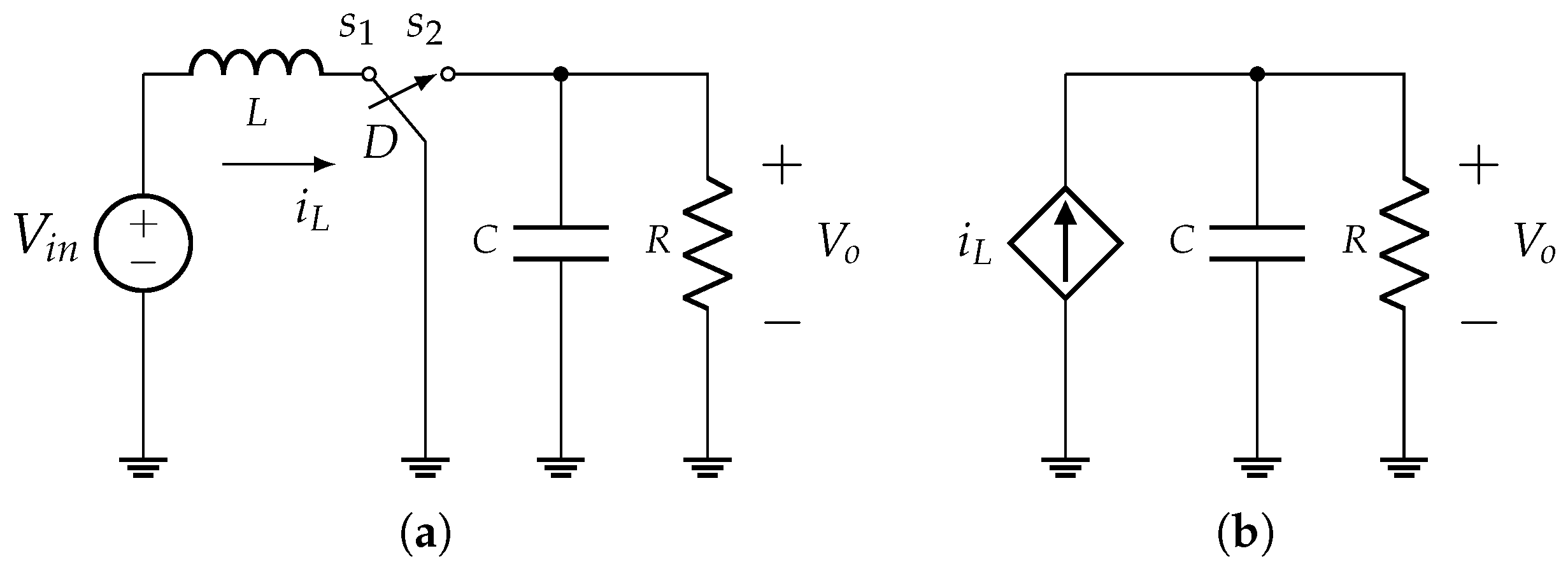
The proposed design methodology is based on the averaged small-signal model of the Boost DC–DC converter shown in Figure 1a. The converter increases the nominal input voltage V i n to an output voltage V o by adjusting the steady-state duty cycle D. Under ideal steady-state conditions, the voltage-conversion ratio is given by [36]
V o V i n = 1 1 − D .
The energy-storage variables of the converter are the inductor current and the output-capacitor voltage. For the averaged small-signal model, i L ( s ) and V o ( s ) denote the inductor-current and output-voltage variations, respectively, while d ( s ) represents the duty-cycle variation. Input-voltage variations around the nominal value V i n are represented by the disturbance V g ( s ) . Thus, V g ( s ) is not an independent physical input, but represents perturbations of the converter input voltage about its nominal operating point. The transfer functions required for the cascade-control design are given by [23]
G i d ( s ) = i L ( s ) d ( s ) = V o C s + 2 V o R L C s 2 + L R s + ( 1 − D ) 2
G v o v g ( s ) = V o ( s ) V g ( s ) = 1 − D L C s 2 + L R s + ( 1 − D ) 2
G i L v g ( s ) = i L ( s ) V g ( s ) = C s + 1 R L C s 2 + L R s + ( 1 − D ) 2
G v o i L ( s ) = V o ( s ) i L ( s ) = R R C s + 1
where V o and D denote the steady-state output voltage and duty cycle, respectively. The transfer function G v o i L ( s ) is obtained by assuming that the inner control loop regulates the inductor current, allowing the circuitry upstream of the output capacitor to be represented by the equivalent current source shown in Figure 1b.
The small-signal model in (13)–(16) assumes ideal converter components and operation in continuous-conduction mode (CCM); therefore, semiconductor losses and parasitic elements are neglected in the control-oriented dynamic model. To maintain CCM and restrict the output-voltage ripple to a prescribed value Δ V o , the inductance and capacitance must satisfy [37]
L > ( 1 − D ) 2 D R 2 f
C > D V o R f Δ V o ,
where f is the switching frequency.
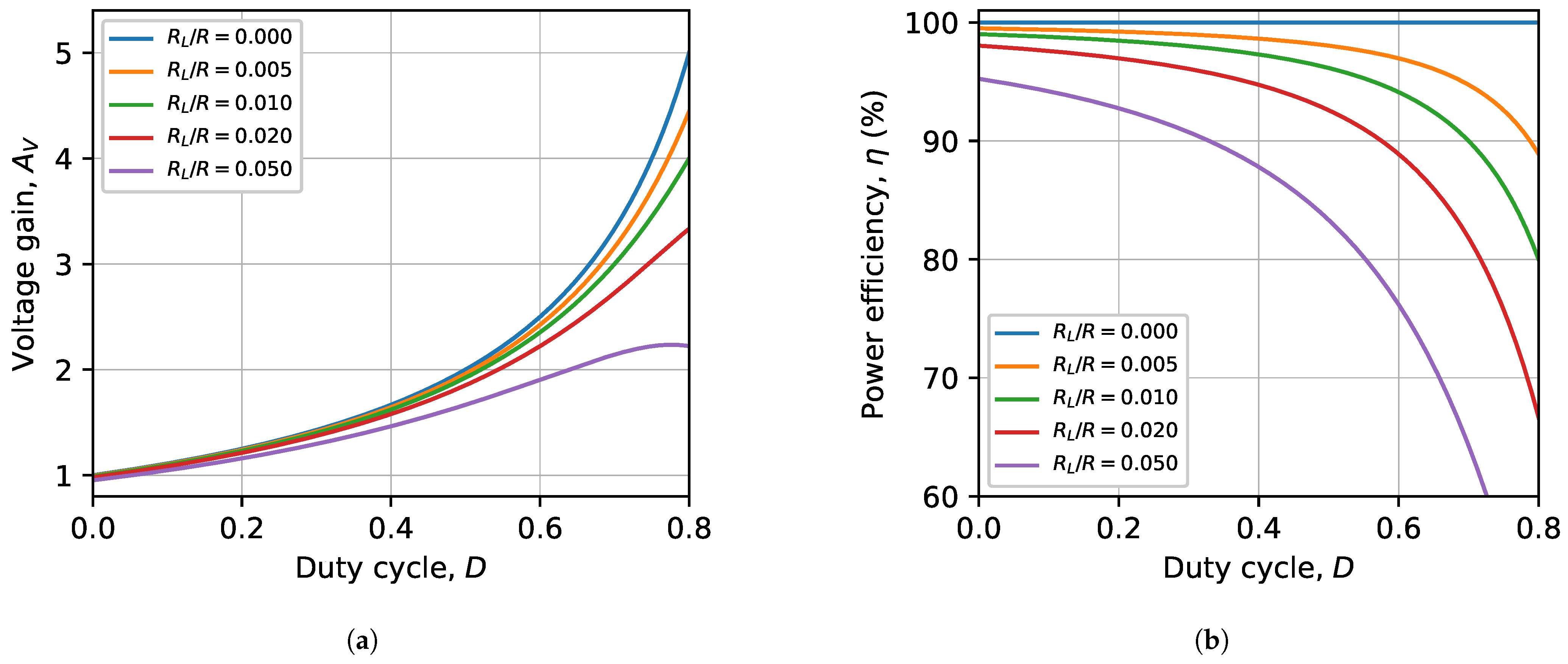
Although parasitic elements are neglected in the control-oriented small-signal model, the influence of the inductor parasitic resistance R L on the steady-state voltage gain and power-conversion efficiency can be evaluated as [38]
A V = V o V i n = 1 1 − D 1 1 + R L ( 1 − D ) 2 R
η = 1 1 + R L ( 1 − D ) 2 R .
Figure 2 illustrates the effect of the duty cycle and normalized inductor parasitic resistance R L / R on the voltage gain and conversion efficiency. Increasing D increases the ideal conversion ratio, whereas increasing R L / R reduces both the achievable voltage gain and efficiency. These relationships illustrate the influence of the duty cycle and inductor parasitic resistance on the steady-state voltage gain and power-conversion efficiency.

2.3. Cascade-Control Structure

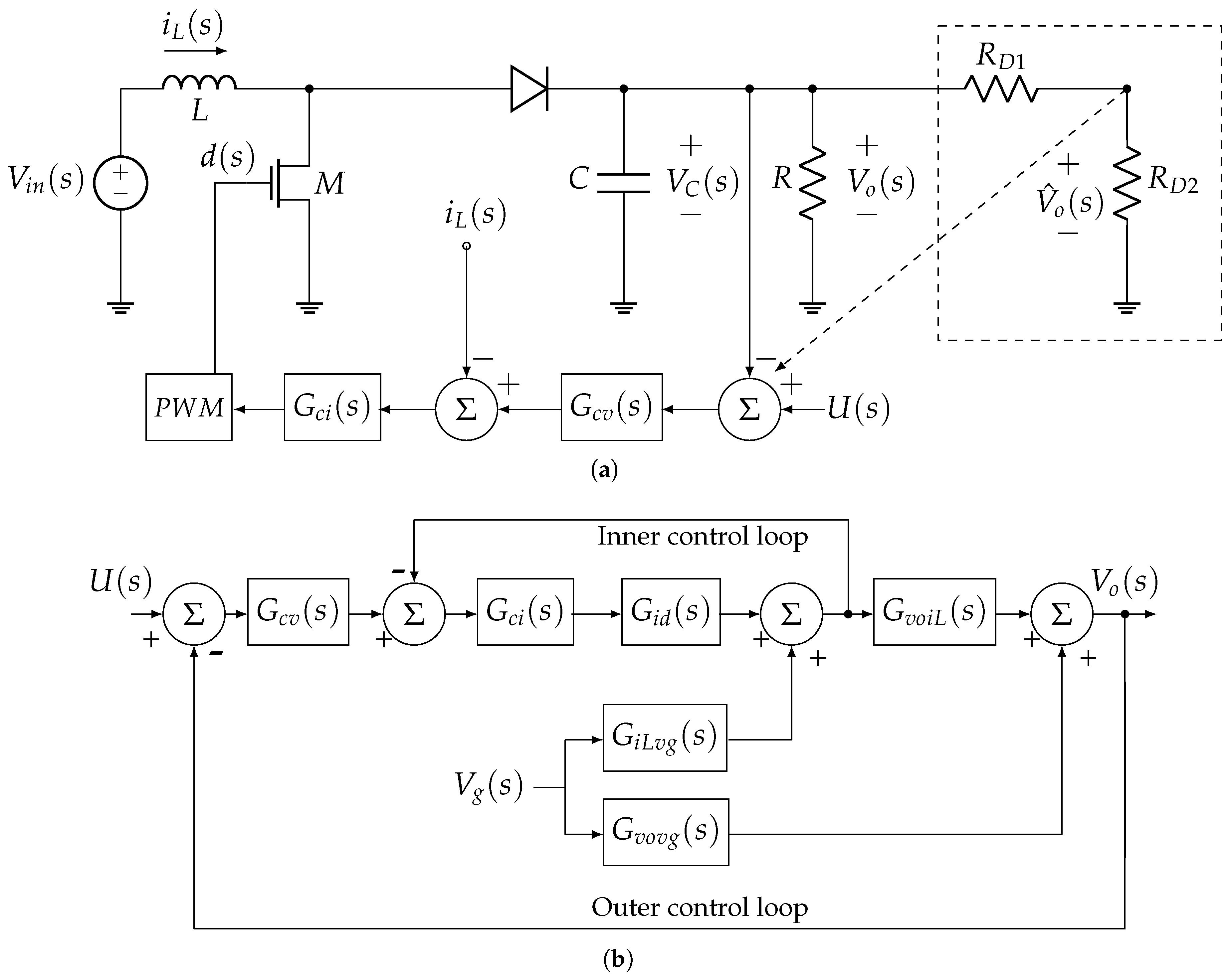
The Boost converter is controlled using a cascade architecture comprising a fast inner current loop and a slower outer voltage loop, as shown in Figure 3a. The inner loop regulates the inductor current, whereas the outer loop regulates the output voltage and generates the current reference required by the inner loop. This separation of the control time scales facilitates the synthesis of the two controllers and improves reference tracking and disturbance rejection. The current-feedback path is assumed to have unity incremental gain in the analytical model; any nonunity current-sensing gain can be incorporated multiplicatively into the inner-loop plant.
The controllers G c i ( s ) and G c v ( s ) correspond to the inner current and outer voltage loops, respectively. The outer voltage controller generates the inductor-current reference for the inner loop, whereas the output of the current controller determines the duty-cycle variation d ( s ) applied to the converter through the pulse-width-modulation (PWM) stage. Since d ( s ) is the control variable of the small-signal converter model, the PWM stage is not explicitly represented in the block diagram used for controller synthesis.
For practical implementation, the output voltage is scaled by the resistive divider formed by R D 1 and R D 2 , as shown in Figure 3a. The resulting feedback voltage V ^ o ( s ) is
V ^ o ( s ) = H v V o ( s ) , H v = R D 2 R D 1 + R D 2 ,
where H v denotes the voltage-feedback gain introduced by the resistive divider, and the reference signal U ( s ) is scaled consistently with the same feedback-voltage range. Assuming that R D 1 + R D 2 ≫ R , so that the divider does not significantly load the converter output, the corresponding transfer functions become
G v o i L ( s ) = V ^ o ( s ) i L ( s ) ≈ R R C s + 1 H v
G v o v g ( s ) = V ^ o ( s ) V g ( s ) = 1 − D L C s 2 + L R s + ( 1 − D ) 2 H v .
For proper cascade operation, the inner current loop is designed to exhibit faster dynamics than the outer voltage loop. Accordingly, the settling-time specifications are selected such that t s , i < t s , v , providing the required separation between the current- and voltage-loop time scales.

2.4. Controller Design Fundamentals

2.4.1. Design Specifications

The desired transient response is characterized using a canonical second-order underdamped model, with the settling time defined according to the 2% criterion. From the prescribed maximum overshoot M p , settling time t s , and steady-state error e s s , the damping ratio ζ , phase margin ϕ m , closed-loop bandwidth ω B W , and required low-frequency loop gain K n are calculated as
ζ = ln M p / 100 π 2 + ln 2 M p / 100 ,
ϕ m = arctan 2 ζ − 2 ζ 2 + 4 ζ 4 + 1 − 1 / 2 ,
ω B W = 4 ζ t s ( 1 − 2 ζ 2 ) + 4 ζ 4 − 4 ζ 2 + 2 ,
and
K n = 100 e s s − 1 .
Here, M p and e s s are expressed as percentages, ϕ m in (25) is obtained in radians and is subsequently expressed in degrees for the frequency-domain design calculations, and t s is expressed in seconds.
For the analytical synthesis, the closed-loop bandwidth obtained from the prescribed transient-response specifications is adopted as an estimate of the target crossover frequency:
ω c ≈ ω B W .

2.4.2. PI and Fractional-Order PI Controllers

The fractional-order P I λ D μ controller generalizes the conventional PID structure by introducing the integration and differentiation orders λ and μ as additional real-valued parameters [39]. Its transfer function is
C ( s ) = K p + K i s λ + K d s μ ,
where K p , K i , and K d are the proportional, integral, and derivative gains, respectively. The conventional PID controller is recovered for λ = μ = 1 .
For the cascade-control problem considered in this work, only proportional and integral actions are required for the reference controllers. Therefore, setting K d = 0 yields the fractional-order PI (FO–PI) controller
C ( s ) = K p + K i s λ ,
which reduces to the conventional PI controller when λ = 1 .
Conventional PI and FO–PI controllers have previously been applied to the inner current and outer voltage loops of the Boost converter considered in this study [40]. These controllers are therefore included as benchmark strategies for comparison with the integer-order and fractional-order lead–lag compensators considered in this work.

2.4.3. Integer-Order Lead–Lag Compensation

Phase-lead and phase-lag compensators modify the frequency response of a system to improve its steady-state and transient performance. Phase-lag compensation is primarily used to increase low-frequency gain, whereas phase-lead compensation provides positive phase and generally increases the achievable bandwidth [41]. Wang [30] proposed an analytical procedure for determining the parameters of a single-stage lead or lag compensator from prescribed magnitude and phase contributions at a selected crossover frequency.
The compensator is defined as
C ( s ) = K 1 + α τ s 1 + τ s ,
where K is the DC gain, and α and τ determine the pole–zero configuration. Using the performance relationships introduced in Section 2.4.1, let M (dB) and p (rad), with − π / 2 ≤ p ≤ π / 2 , denote the required magnitude and phase contributions of the compensator at the crossover frequency ω c , respectively. Defining c = 10 M / 20 and δ = tan ( p ) , a single-stage solution exists if [30]
c > 1 + δ 2 , 0 < p ≤ π / 2 ( phase lead )
c < 1 1 + δ 2 , − π / 2 ≤ p < 0 ( phase lag ) .
When the corresponding feasibility condition is satisfied, the compensator parameters are obtained analytically as
α = c c 1 + δ 2 − 1 c − 1 + δ 2
τ = c − 1 + δ 2 c δ ω c .
If neither condition is satisfied, the prescribed magnitude and phase contributions cannot be simultaneously achieved by the single-stage compensator in (31).

2.4.4. Fractional-Order Lead–Lag Compensation

Tavazoei [31] extended Wang’s analytical procedure to fractional-order phase-lead and phase-lag compensation by introducing the fractional order q as an additional degree of freedom. The resulting compensator is defined as
C f ( s ) = K 1 + α τ s q 1 + τ s q , q ∈ ( 0 , 2 ) .
Using the same definitions of K, c, p, and ω c introduced for the integer-order compensator, a single-stage fractional-order solution exists if the corresponding feasibility condition is satisfied [31]:
cot q π 2 < c cos ( p ) − 1 c sin ( p ) , 0 < p ≤ π 2 ( phase lead )
cot q π 2 < c − cos ( p ) sin ( p ) , − π 2 ≤ p < 0 ( phase lag ) .
When the corresponding feasibility condition is satisfied, the compensator parameters are obtained analytically as
α = a b tan q π 2 − 1 b tan q π 2 − 1
τ = 1 ω c q b sin q π 2 − cos q π 2 ,
where the auxiliary variables a and b are defined as
a = c c − cos ( p ) c cos ( p ) − 1
b = c cos ( p ) − 1 c sin ( p ) .
In addition to satisfying the prescribed magnitude and phase contributions at ω c , the fractional order q provides an additional degree of freedom that can be used to impose a prescribed initial control-signal value u 0 . For a step input and phase-lead compensation, u 0 ∈ ( K , ∞ ) and q is determined as [31]
q = 2 π tan − 1 u 0 − K b ( u 0 − K a ) , if b ( u 0 − K a ) > 0 1 , if b ( u 0 − K a ) = 0 2 + 2 π tan − 1 u 0 − K b ( u 0 − K a ) , if b ( u 0 − K a ) < 0
For phase-lag compensation, u 0 ∈ ( 0 , K ) and the corresponding fractional order is
q = 2 + 2 π tan − 1 u 0 − K b ( u 0 − K a ) , if b ( u 0 − K a ) > 0 1 , if b ( u 0 − K a ) = 0 2 π tan − 1 u 0 − K b ( u 0 − K a ) , if b ( u 0 − K a ) < 0 .
Thus, unlike the integer-order compensator, the fractional-order formulation allows the initial control effort to be explicitly incorporated as a design constraint while preserving the analytical nature of the synthesis procedure.

2.4.5. Rational Approximation for Electronic Realization

For practical implementation, the fractional-order operator s q in (36) must be represented by an integer-order rational approximation. Using the first-order CFE approximation in (5), two cases arise depending on the value of q.
  • Case I ( 0 < q < 1 ): The fractional-order compensator is approximated as
C f ( s ) ≈ K 1 + α τ A 1 1 + τ A 1 s + A 1 + α τ 1 + α τ A 1 s + A 1 + τ 1 + τ A 1 ,
where A 1 is given by (7).
  • Case II ( 1 < q < 2 ): Defining q ˜ = q − 1 , the fractional operator can be written as s q = s s q ˜ , where 0 < q ˜ < 1 . Applying (5) to s q ˜ gives
C f ( s ) ≈ K 1 + α τ s A 1 s + 1 s + A 1 1 + τ s A 1 s + 1 s + A 1 = α K s 2 + ω z Q z s + ω z 2 s 2 + ω p Q p s + ω p 2 ,
where A 1 is obtained from (7) by replacing q with q ˜ , and
ω p = 1 τ ,
Q p = τ A 1 τ + 1 ,
ω z = 1 α τ ,
Q z = α τ A 1 α τ + 1 .
For q = 1 , no rational approximation is required, since (36) directly reduces to the corresponding integer-order lead–lag compensator. Therefore, (45) and (46) provide first-order rational realizations over the two fractional-order intervals 0 < q < 1 and 1 < q < 2 , respectively.

3. Design and Evaluation Methodology

This section presents the methodology adopted for both the integrated analytical design and the systematic numerical evaluation of the Boost DC–DC converter and its cascade control system. The methodology is organized into two complementary stages. First, the power stage and the inner current and outer voltage controllers are obtained through an integrated analytical design procedure starting from prescribed electrical and closed-loop performance specifications. Second, the resulting controllers are systematically evaluated under nominal and perturbed operating conditions using the averaged small-signal representation of the converter. This organization separates the proposed engineering design procedure from the numerical framework subsequently used to assess nominal performance, sensitivity to the fractional-order approximation, operating-point dependence, robustness to converter-parameter variations, sensitivity to controller-component tolerances, and load-disturbance rejection.

3.1. Integrated Analytical Design Procedure

The proposed design procedure integrates the sizing of the Boost power stage with the sequential analytical synthesis of its cascade current-mode control system. Starting from the electrical specifications of the converter and the prescribed transient- and steady-state performance requirements, the procedure sequentially determines the power-stage parameters, the inner current controller, and the outer voltage controller. Controller synthesis is performed using either the integer-order analytical method of Wang et al. [30] or its fractional-order extension by Tavazoei et al. [31], within the integrated design sequence that subsequently includes electronic realization, commercial component selection, and implementation-oriented verification.
The power-stage design starts from the input voltage V i n , desired output voltage V o , rated output power P o , switching frequency f, and admissible output-voltage ripple Δ V o . The nominal duty cycle and load resistance are obtained from the steady-state operating conditions, whereas the inductance L and capacitance C are selected using the design relationships in Section 2.2 so that the prescribed ripple requirements are satisfied and continuous-conduction-mode operation is maintained. Once the power-stage parameters and nominal operating point have been established, the averaged small-signal model is evaluated to obtain G i d ( s ) and G v o i L ( s ) , which constitute the plant models required for the sequential cascade-controller design.
For each control loop, the prescribed values of M p , t s , and e s s are mapped into the damping ratio ζ , phase margin ϕ m , target bandwidth ω B W , and required low-frequency loop gain K n using the analytical relationships introduced in Section 2.4.1. For controller synthesis, the target crossover frequency is selected as ω c ≈ ω B W , using the closed-loop bandwidth as an approximation of the desired loop crossover frequency. Consistent with the cascade-control requirement established in Section 2.3, the settling-time specifications are selected such that t s , i < t s , v , ensuring faster inner-loop dynamics.
The inner current loop is designed first using G i d ( s ) . After the inner loop is closed, its dynamics are incorporated into the effective plant seen by the outer voltage loop through the cascade structure defined in Section 2.3. The outer voltage controller is then synthesized from the corresponding voltage-loop specifications. Consequently, the inner-loop dynamics are explicitly included in the outer-loop design rather than treating the two controllers independently. For each loop, the integer-order and fractional-order designs share the same performance specifications and plant model; however, the fractional-order formulation introduces the order q as an additional design variable and incorporates the prescribed initial control signal u 0 as an additional synthesis constraint.
For the integer-order design, Wang’s analytical relationships are used to determine the compensator gain, phase contribution, and pole–zero parameters directly from the prescribed performance requirements and the uncompensated frequency response. For the fractional-order design, the same sequential procedure is followed, but the fractional order q provides an additional degree of freedom that is used to prescribe the initial control-signal value u 0 . Thus, the fractional-order formulation incorporates a control-effort constraint directly into the analytical synthesis while retaining the magnitude and phase requirements at the target crossover frequency. No numerical optimization or iterative controller tuning is required in either design procedure.
The analytically obtained fractional-order controllers are subsequently expressed in the rational forms described in Section 2.4.5, providing the connection between the analytical synthesis, numerical simulation, and practical electronic realization. Integer-order compensators can be implemented directly using conventional operational-amplifier circuits, whereas fractional-order compensators are first represented through the corresponding CFE rational approximation. The resulting transfer functions are then used to determine the resistor and capacitor values of the analog realizations.
To enable direct comparison with the controllers reported in [23,40], the electrical specifications and component values of the converter considered in those studies are adopted for the comparative case study presented here. Thus, although power-stage sizing forms part of the general methodology, the previously reported converter is retained in this case to provide a common plant for controller comparison. The resulting parameters are summarized in Table 2.
For consistency with [23,40], the voltage-divider network R D 1 – R D 2 is omitted in the comparative case study. Substitution of the parameters in Table 2 into the averaged small-signal model yields
G i d ( s ) = 48,000 s + 2,000,000 s 2 + 20.83 s + 250,000 , G v o i L ( s ) = 120 0.048 s + 1 .
The proposed controllers are benchmarked against the integer-order and fractional-order PI controllers reported in [40]. In that work, the IO–PI and FO–PI controllers were designed using SISOTOOL. The inner current loop was tuned for a damping ratio of ζ = 0.707 ( M p = 4.3 % ), while maintaining the closed-loop bandwidth below one-fifth of the switching frequency. The same damping-ratio specification was adopted for the outer voltage loop. The resulting controllers are
G c i ( s ) = 0.3040 + 2172 s λ , G c v ( s ) = 0.2507 + 61.15 s λ ,
where λ = 1 and λ = 0.5 correspond to the IO–PI and FO–PI implementations, respectively.
The design specifications adopted for the proposed compensators were selected to provide transient-response requirements comparable to those achieved by the IO–PI controllers reported in [40]. The FO–PI controllers were not used as the reference for selecting these specifications because their substantially faster responses are accompanied by excessively large control signals, as discussed in Section 4. In the proposed fractional-order design, this limitation is explicitly addressed by imposing a prescribed constraint on the initial control signal.
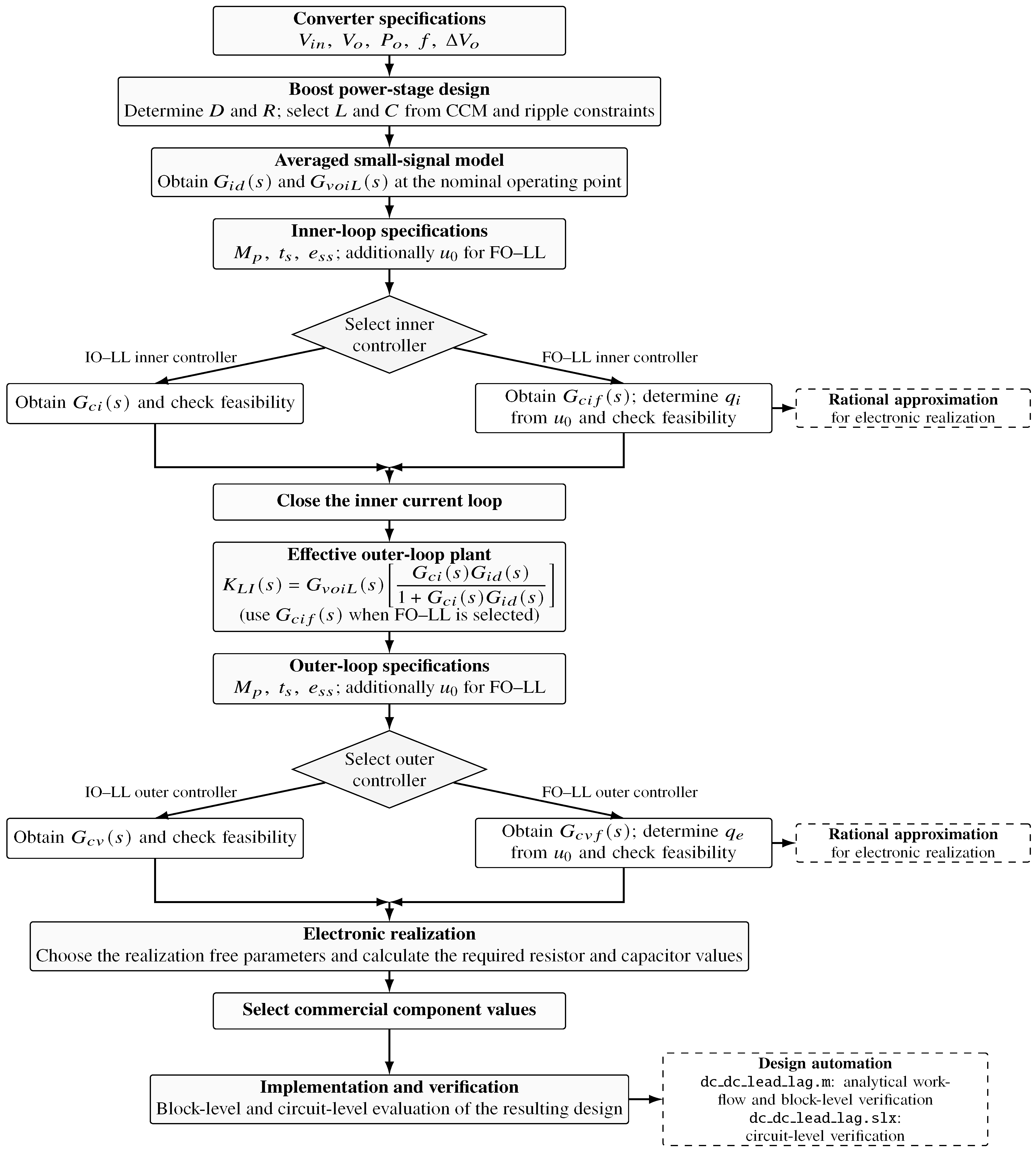
The complete integrated design procedure is summarized in Figure 4.
Starting from the converter specifications and the prescribed closed-loop performance requirements, the procedure sequentially addresses Boost power-stage sizing, small-signal modeling, inner current-loop design, construction of the effective outer-loop plant, outer voltage-loop design, and electronic realization. Integer- or fractional-order lead–lag compensation can be selected independently for each loop. The resulting controller parameters are subsequently translated into practical component values for implementation and verification.

3.1.1. Integer-Order Design Procedure

The integer-order design procedure applies Wang’s analytical method sequentially to the inner current and outer voltage loops. The corresponding compensators are defined as
G c i ( s ) = K i n t 1 + α i τ i s 1 + τ i s ,
G c v ( s ) = K e x t 1 + α e τ e s 1 + τ e s .
The design is carried out according to the following procedure:
1.
Specify the desired values of M p , t s , and e s s for the inner and outer control loops.
2.
Calculate ζ , ϕ m , ω B W , and K n from (24)–(27). The parameter K n represents the low-frequency loop gain required to satisfy the prescribed steady-state error. For controller synthesis, the target crossover frequency is approximated as ω c ≈ ω B W .
3.
Design the inner current loop. Since G i d ( 0 ) contributes to the low-frequency loop gain, the DC gain required from the inner compensator is
K i n t = K n G i d ( 0 ) .
Evaluate the magnitude and phase of K i n t G i d ( j ω c ) . Denoting the uncompensated-loop phase at ω c by ϕ u , calculate the required phase contribution as
p = − π + ϕ m − ϕ u .
The required magnitude contribution M is the negative of the uncompensated-loop magnitude, expressed in decibels.
4.
Calculate c = 10 M / 20 and δ = tan ( p ) , verify the corresponding feasibility condition in (32) or (33), and calculate α i and τ i from (34) and (35).
5.
Once the inner current controller has been obtained, form the equivalent plant for the outer-loop design as
K L I ( s ) = G v o i L ( s ) G c i ( s ) G i d ( s ) 1 + G c i ( s ) G i d ( s ) .
Thus, K L I ( s ) includes the closed inner current loop connected in series with the current-to-output-voltage dynamics G v o i L ( s ) .
6.
Design the outer voltage loop. Since K L I ( 0 ) now contributes to the low-frequency gain of the outer loop, the DC gain required from the outer compensator is
K e x t = K n K L I ( 0 ) .
Evaluate the magnitude and phase of K e x t K L I ( j ω c ) and determine the required compensator contributions M and p as in Step 3. Calculate c and δ , verify the corresponding feasibility condition, and obtain α e and τ e from (34) and (35).
7.
Construct G c i ( s ) and G c v ( s ) from (53) and (54) and evaluate the resulting cascade-controlled system against the prescribed performance specifications.
For the comparative case study, the inner-loop specifications are M p < 5 % , t s = 0.35  ms, and e s s < 0.15 % , whereas the outer-loop specifications are M p < 5 % , t s = 11  ms, and e s s < 0.2 % . The resulting design parameters are summarized in Table 3.
Using the parameters in Table 3, the inner-loop compensator is
G c i ( s ) = 83.21 1 + ( 0.00383 ) ( 0.0324 ) s 1 + 0.0324 s ,
whereas the outer-loop compensator is
G c v ( s ) = 4.16 1 + ( 0.04535 ) ( 0.0736 ) s 1 + 0.0736 s .
The resulting compensators are subsequently evaluated against the prescribed transient- and steady-state performance specifications.

3.1.2. Fractional-Order Design Procedure

The fractional-order design follows the same sequential cascade procedure described in Section 3.1.1. Therefore, the calculation of ζ , ϕ m , ω B W , K n , K i n t , and K e x t , as well as the construction of the equivalent outer-loop plant after closing the inner loop, follows the same sequence as in the integer-order case. The additional fractional orders q i and q e are used to impose prescribed initial control-signal values on the inner and outer loops, respectively.
The design is carried out according to the following procedure:
1.
Specify M p , t s , e s s , and the initial control signal u 0 for each loop. Calculate ζ , ϕ m , ω B W , K n , and the corresponding controller gain following Steps 1–3 of Section 3.1.1, with ω c ≈ ω B W .
2.
For the inner current loop, evaluate the magnitude and phase of K i n t G i d ( j ω c ) and determine the required magnitude contribution M and phase contribution p as in the integer-order procedure. Calculate c = 10 M / 20 and the auxiliary parameters a and b from (41) and (42).
3.
Using the prescribed initial control signal u 0 , i , calculate q i from (43) or (44), according to the required phase contribution. Verify the corresponding feasibility condition in (37) or (38); if it is satisfied, calculate α i and τ i from (39) and (40) and construct G c i f ( s ) .
4.
Close the fractional-order inner current loop and form the equivalent outer-loop plant as
K L I f ( s ) = G v o i L ( s ) G c i f ( s ) G i d ( s ) 1 + G c i f ( s ) G i d ( s ) .
Determine K e x t from the low-frequency gain requirement following the same procedure used for the integer-order outer loop.
5.
For the outer voltage loop, evaluate the magnitude and phase of K e x t K L I f ( j ω c ) and calculate M, p, c, a, and b. Using u 0 , e , determine q e , verify the corresponding fractional-order feasibility condition, and calculate α e and τ e to construct G c v f ( s ) .
6.
For numerical simulation and electronic realization, obtain the rational approximations of G c i f ( s ) and G c v f ( s ) using (45) for 0 < q < 1 or (46) for 1 < q < 2 .
For the comparative case study, the inner-loop specifications are M p = 5 % , t s = 5  ms, e s s = 0.15 % , and u 0 , i = 4 , whereas the outer-loop specifications are M p = 5 % , t s = 11  ms, e s s = 0.2 % , and u 0 , e = 3.5 . The resulting fractional-order design parameters are summarized in Table 4.
Using the parameters in Table 4, the inner-loop compensator is
G c i f ( s ) = 83 1 + ( 0.04819 ) ( 1.4925 × 10 − 5 ) s 1.9987 1 + 1.4925 × 10 − 5 s 1.9987 ,
whereas the outer-loop compensator is
G c v f ( s ) = 4 1 + ( 0.8750 ) ( 4.0165 × 10 − 6 ) s 1.9975 1 + 4.0165 × 10 − 6 s 1.9975 .
Since 1 < q i , q e < 2 , the first-order CFE approximation in (46) is applied to both compensators. The resulting rational approximations are
G c i f ( s ) = 4 s 2 + 3582.94 s + 5.5611 × 10 6 s 2 + 43.1686 s + 6.70012 × 10 4 ,
and
G c v f ( s ) = 3.5 s 2 + 1258.91 s + 9.9589 × 10 5 s 2 + 314.727 s + 2.48973 × 10 5 .

3.1.3. Electronic Realization

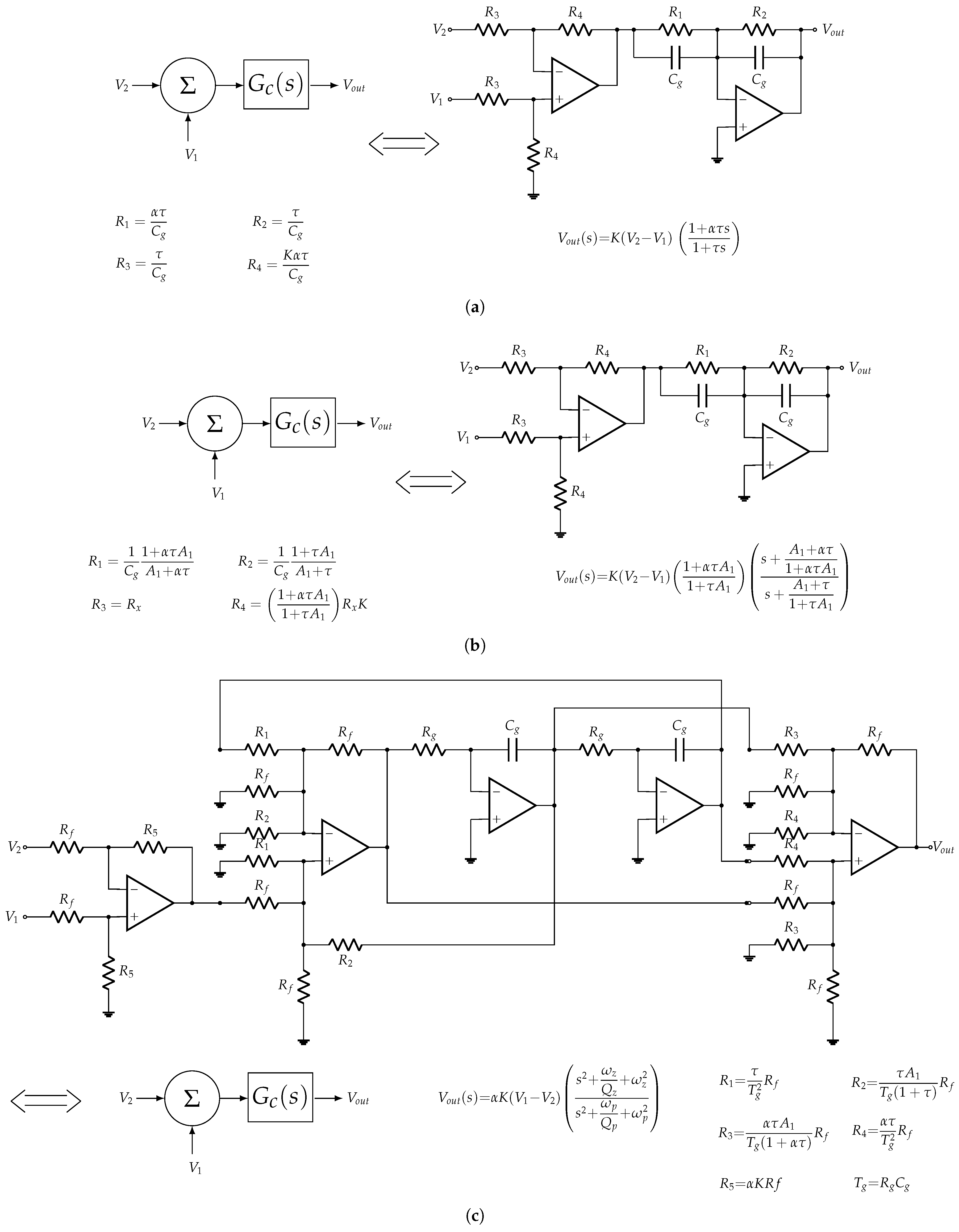
The analytically obtained controllers are implemented using the operational-amplifier circuits shown in Figure 5. The same realization procedure applies to both control loops by taking K = K i n t , α = α i , and τ = τ i for the inner controller, or K = K e x t , α = α e , and τ = τ e for the outer controller.
For the integer-order compensator, the circuit in Figure 5a is employed. After selecting the capacitor C g as a free design parameter, the resistor values R 1 – R 4 are obtained directly from K, α , τ , and C g according to the relationships indicated in the figure.
For a fractional-order compensator with 0 < q < 1 , the circuit in Figure 5b is used. The values of C g and R x are selected as free design parameters, and A 1 is calculated from (7). The resistor values R 1 – R 4 are then determined from K, α , τ , A 1 , R x , and C g using the relationships indicated in the figure.
For 1 < q < 2 , the circuit in Figure 5c is employed. In this case, the fractional power is expressed as s q = s s q ˜ , where q ˜ = q − 1 , as described in Section 2.4.5. The electronic realization provides two effective degrees of freedom: the time-scaling factor T g and the impedance-scaling resistance R f . The former is implemented through the product of R g and C g ,
T g = R g C g .
Thus, after selecting T g and R f , either R g or C g can be chosen according to practical component-value considerations, with the remaining component determined from T g = R g C g . The parameter A 1 is calculated from (7) using q ˜ . The remaining resistor values are then obtained as
R 1 = τ T g 2 R f , R 2 = τ A 1 T g ( 1 + τ ) R f ,
R 3 = α τ A 1 T g ( 1 + α τ ) R f , R 4 = α τ T g 2 R f ,
R 5 = α K R f .
The resulting nominal component values for the practical operational-amplifier realizations of the inner and outer IO–LL and FO–LL controllers are summarized in Table 5.

3.1.4. Design Automation

The analytical formulation of the proposed methodology enables the complete design procedure to be automated without optimization-based or trial-and-error controller tuning. Consequently, an implementation based on MATLAB R2026a, Simulink, and Simscape Electrical was developed to automate the Boost-converter design, cascade-controller synthesis, electronic realization, and post-design simulation-based verification, without using the numerical evaluation results to retune the analytically obtained controllers. The developed files are provided as Supplementary Materials to reproduce the analytical design procedure, the corresponding block-level verification, and the circuit-level implementation described below.
The MATLAB script dc_dc_lead_lag.m receives the converter electrical specifications and the prescribed performance requirements for the inner and outer control loops. For fractional-order compensation, the desired initial control-signal constraints u 0 , i and u 0 , e are additionally specified. From these inputs, the program determines suitable power-stage parameters satisfying the continuous-conduction-mode and output-voltage-ripple constraints in (17) and (18), obtains the corresponding small-signal transfer functions, and applies the analytical procedures described in Section 3.1.1 and Section 3.1.2. Integer- or fractional-order compensation can be independently selected for each control loop.
The program subsequently calculates the controller parameters, the rational approximations required for fractional-order implementation, and the component values of the corresponding operational-amplifier realizations. It also generates the frequency and transient responses required for preliminary verification of the resulting design.
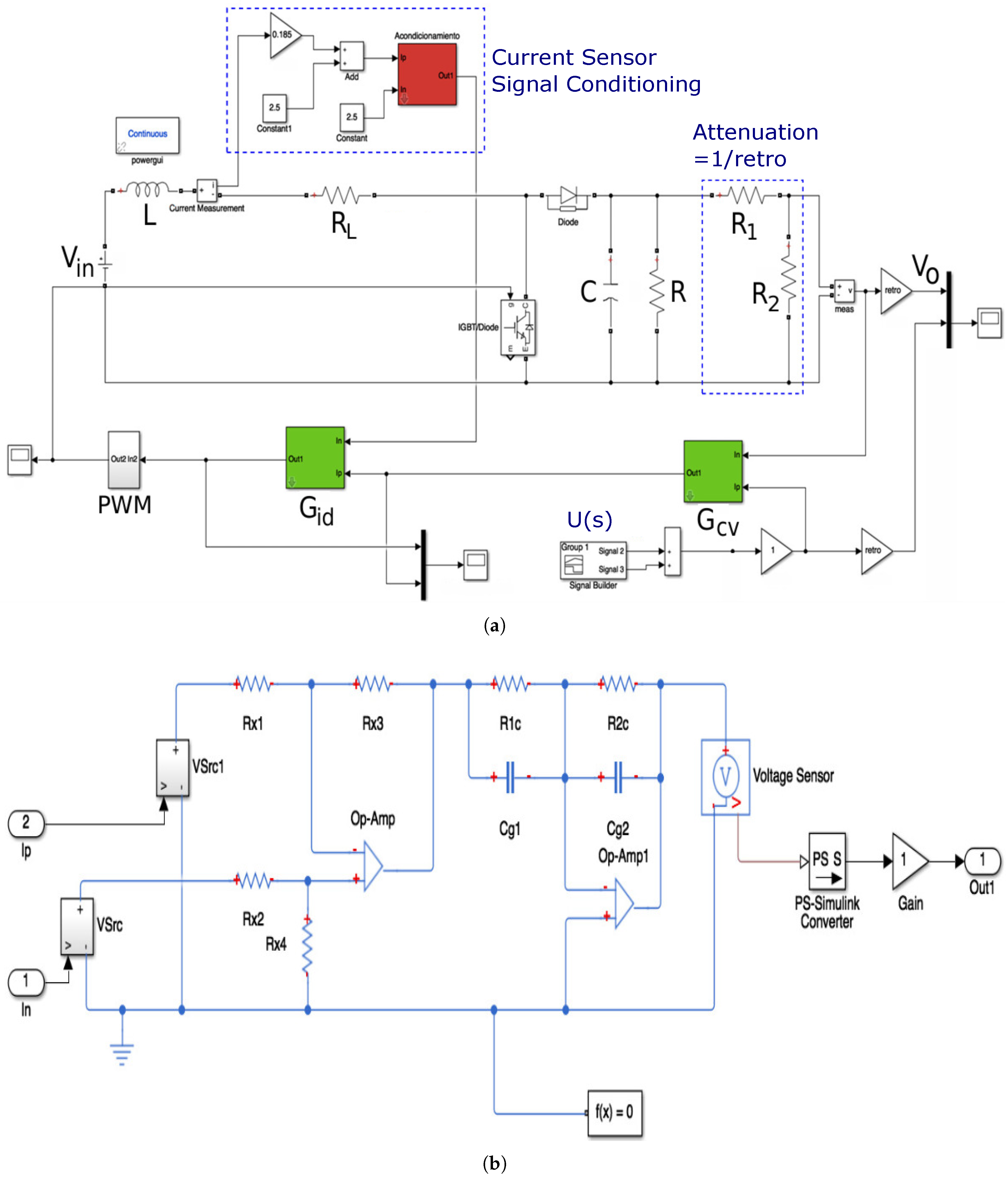
Circuit-level verification is performed using the Simulink/Simscape Electrical model dc_dc_lead_lag.slx, illustrated in Figure 6. The model incorporates the Boost converter shown in Figure 6a and the operational-amplifier controller realizations shown in Figure 6b, using the parameters calculated by the MATLAB script.
Thus, the developed software provides a reproducible automated workflow from converter and closed-loop performance specifications to power-stage sizing, analytical controller synthesis, electronic realization, and simulation-based verification, while preserving the analytical nature of the proposed design methodology.
The supplied MATLAB script reproduces the analytical controller-design procedure, the corresponding block-level verification, and the first- and third-order CFE rational approximations available within the design software. The first-order approximation is the one adopted for the practical analog realization and the associated circuit-level implementation reproduced with the supplied Simulink/Simscape model. The additional fifth- and seventh-order CFE sensitivity results, Monte Carlo converter-parameter analysis, and controller-component-tolerance analysis reported in Section 4 constitute post-design validation studies and are not generated by the supplied Supplementary Files.

3.2. Numerical Evaluation Methodology

The controllers obtained through the integrated analytical design procedure are systematically evaluated using the averaged small-signal representation of the Boost converter and the cascade-control structure defined in Section 2. The numerical evaluation considers nominal closed-loop performance, sensitivity to the fractional-order approximation, reference tracking and input-voltage disturbance rejection, operation away from the nominal design point, robustness to converter-parameter variations, robustness to controller-component tolerances, and load-disturbance rejection. Unless otherwise stated, the controllers are kept fixed at their nominal design values throughout the robustness analyses.
The IO–LL and FO–LL controllers are first evaluated under nominal operating conditions and compared with the IO–PI and FO–PI benchmark controllers. The inner current loop and the complete cascade-controlled voltage loop are analyzed separately using their corresponding reference changes. Closed-loop performance is characterized in terms of maximum overshoot M p , settling time t s , steady-state error e s s , maximum control action u max , integral absolute error (IAE), and integral squared control variation (ISU). The first four quantities allow direct verification of the principal design and control-effort requirements, whereas IAE and ISU provide complementary measures of tracking performance and control effort. Because the unconstrained FO–PI produces large control amplitudes, an additional case with an ideal ±5 V output saturation is included to provide an amplitude-limited benchmark.
Because the fractional-order controllers require rational approximations for numerical simulation and practical realization, the influence of the Continued Fraction Expansion (CFE) approximation order is evaluated separately. Different CFE orders are applied while maintaining the analytically obtained fractional-order controller parameters unchanged; therefore, the approximation-order study constitutes a post-design sensitivity evaluation and is not used for controller tuning. The resulting transient responses and control signals are compared to assess the sensitivity of the closed-loop performance to the approximation order and to verify whether a low-order approximation preserves the intended controller behavior.
Reference tracking and input-voltage disturbance rejection are subsequently evaluated by applying successive output-voltage reference changes while superimposing a 10 kHz sinusoidal perturbation with an amplitude equal to 5% of the nominal input voltage. The disturbance is introduced through both the input-voltage-to-inductor-current and input-voltage-to-output-voltage transfer functions. The resulting output-voltage and inductor-current responses are used to assess tracking capability and disturbance attenuation.
The dependence of the closed-loop response on the converter operating point is evaluated for D = { 0.40 , 0.45 , 0.50 , 0.55 , 0.60 } . For each duty cycle, the corresponding steady-state output voltage and averaged small-signal model are recalculated, while the controllers remain fixed at the values obtained for the nominal condition D = 0.5 . A local +10% output-voltage reference step is applied around each operating point. This analysis evaluates the ability of the nominal controller designs to preserve their closed-loop behavior over the considered operating range without retuning.
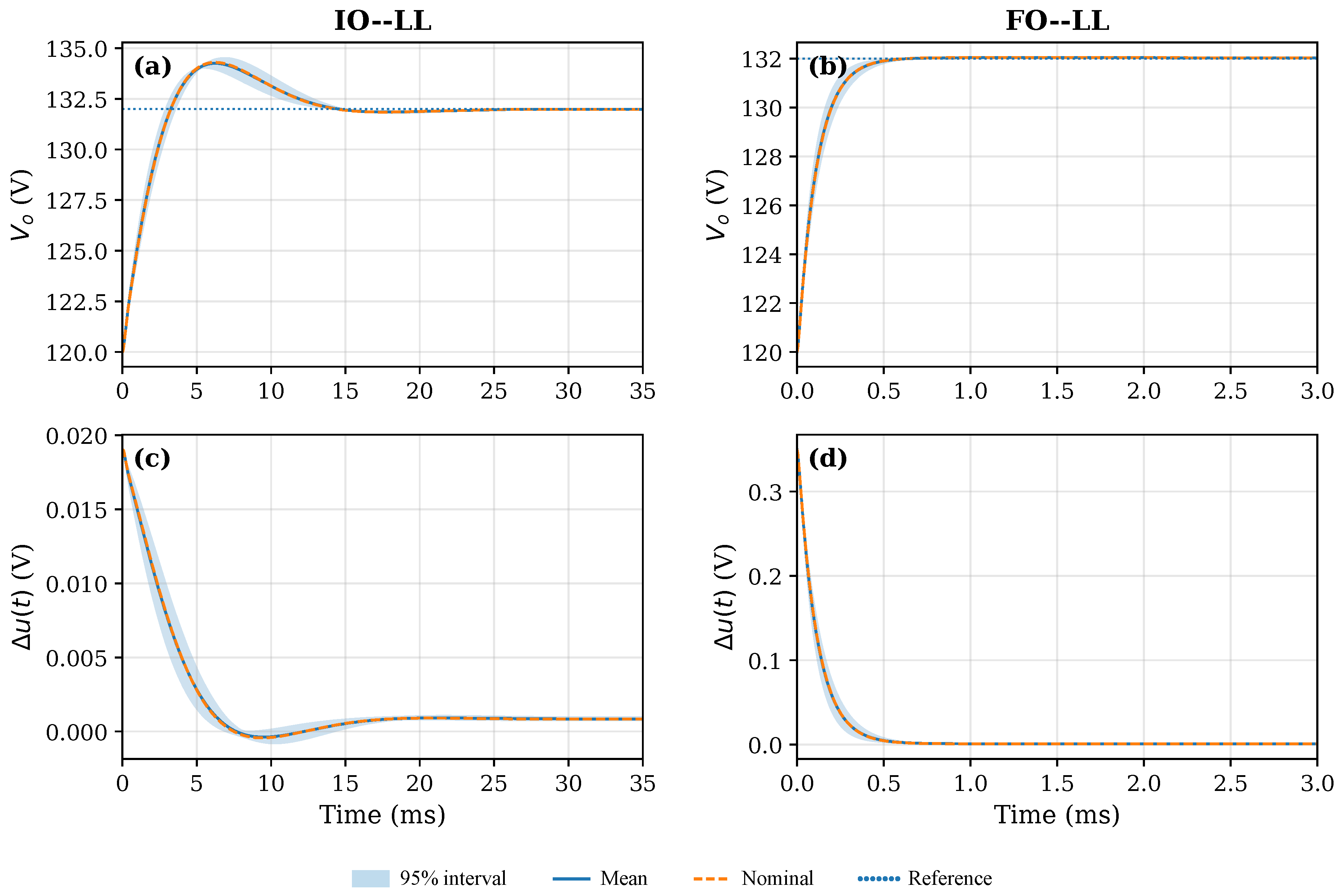
Robustness to converter-parameter variations is evaluated through a Monte Carlo analysis with N = 1000 realizations. The inductance L, capacitance C, and load resistance R are independently varied according to uniform distributions within ±20% of their nominal values. The controllers remain fixed at their nominal values, and the operating condition is maintained at D = 0.5 , V i n = 60  V, and V o 0 = 120  V. A reference step from 120 to 132 V is applied in each realization, and the resulting distributions of the closed-loop performance indices are used to compare the sensitivity of the IO–LL and FO–LL designs to simultaneous converter-parameter variations.
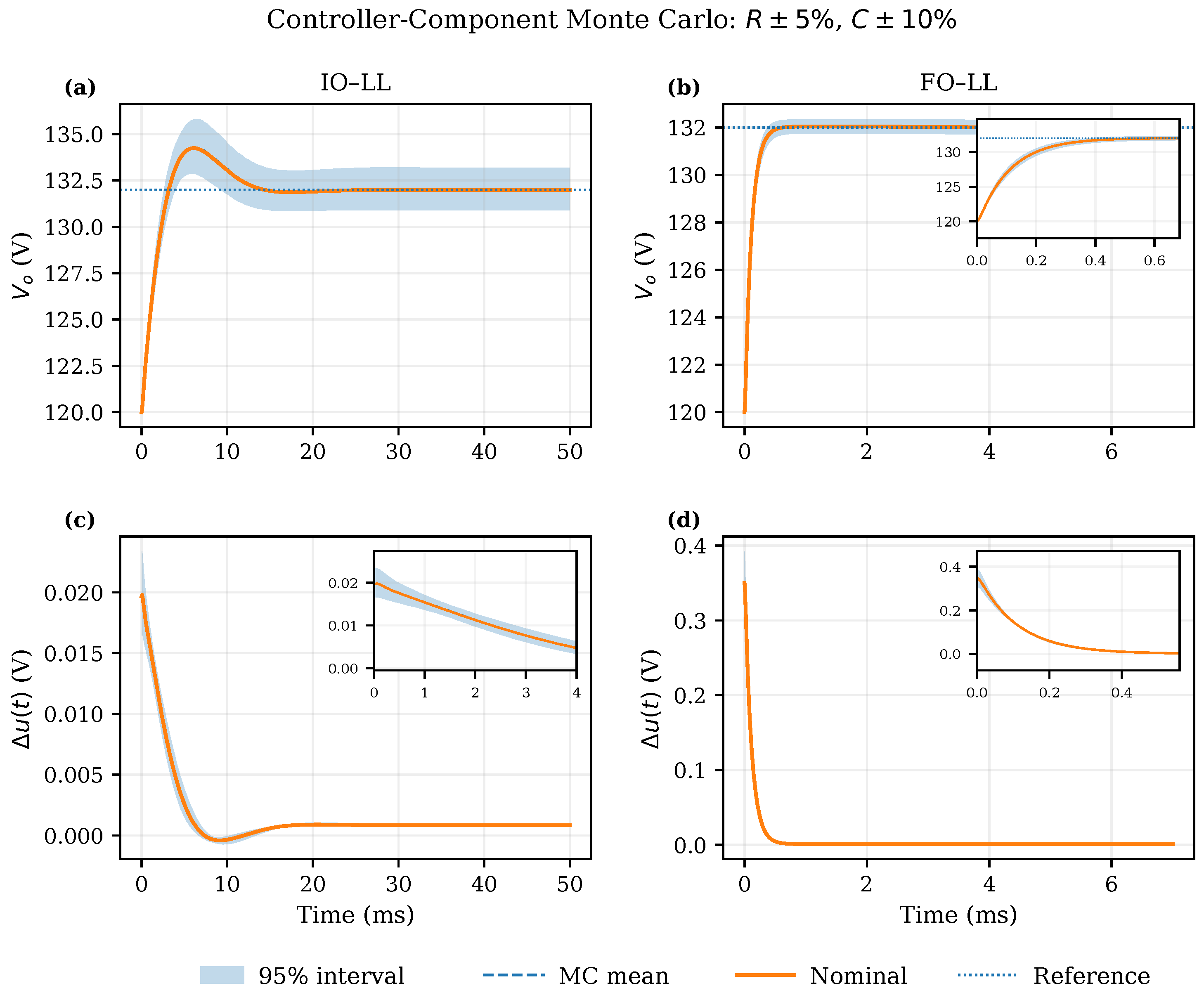
A second Monte Carlo analysis with N = 1000 realizations evaluates the robustness of the controller implementations to physical component tolerances. Every resistor and capacitor in the inner- and outer-loop IO–LL and FO–LL circuits is independently varied using uniform distributions, considering tolerances of ±5% for resistors and ±10% for capacitors, without assuming matched components. In this case, the converter parameters are maintained at their nominal values. For each realization, the controller transfer functions resulting from the perturbed circuit components are reconstructed and the complete closed-loop response is evaluated for the same 120–132 V reference step. This analysis quantifies the sensitivity introduced by the practical analog realization independently of converter-parameter uncertainty.
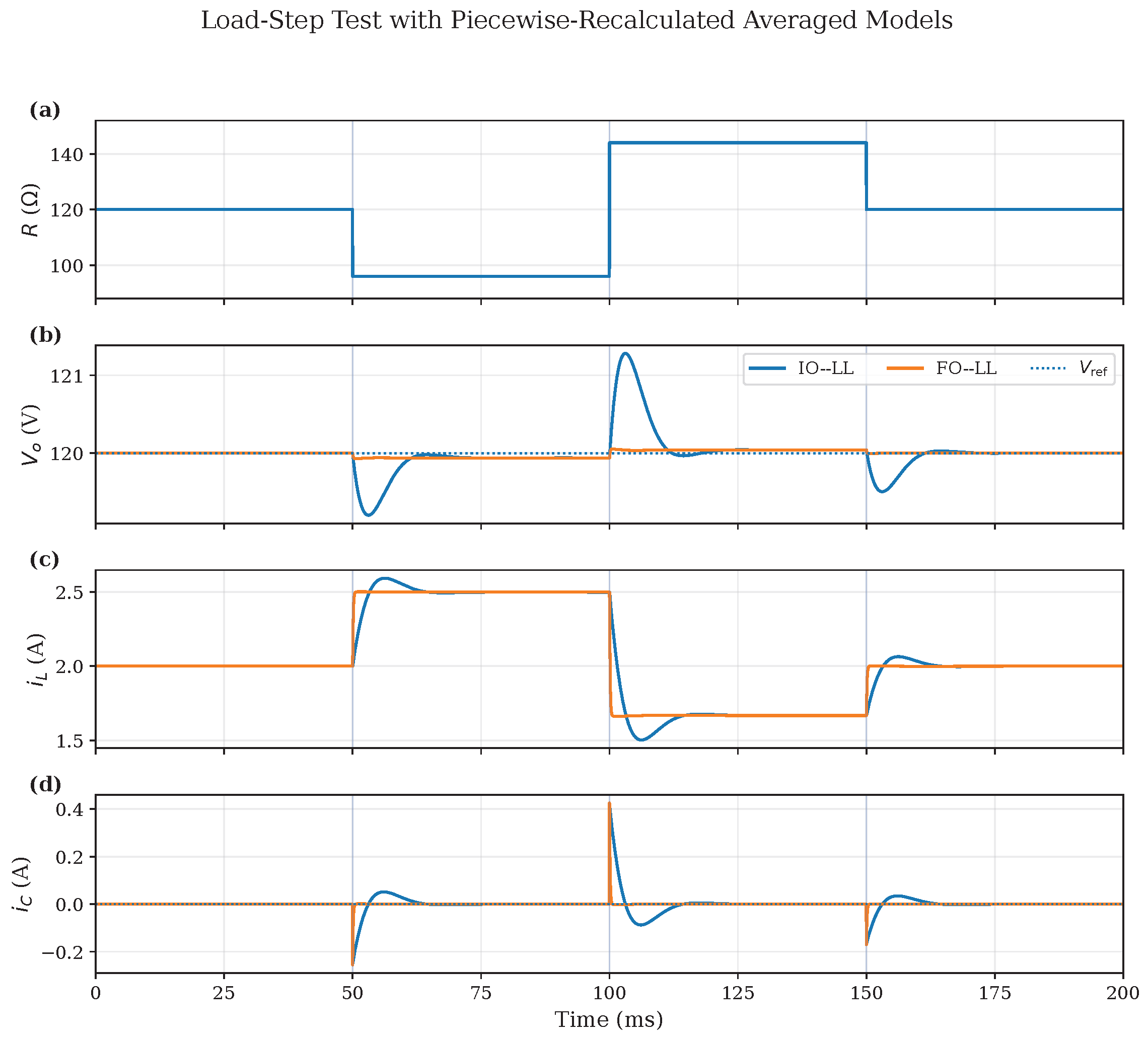
Finally, load-disturbance rejection is evaluated with the output-voltage reference fixed at V ref = 120  V. The load resistance is sequentially changed according to
120 → 96 → 144 → 120   Ω
at t = 50 , 100, and 150 ms, respectively, while the controllers remain unchanged. The resulting output-voltage, inductor-current, and capacitor-current responses are analyzed to assess the capability of the IO–LL and FO–LL implementations to reject load disturbances and recover the regulated output voltage.
Together, these numerical experiments provide a systematic assessment of nominal performance, fractional-order approximation sensitivity, operating-point dependence, robustness to converter-parameter variations, sensitivity to physical controller-component tolerances, and load-disturbance rejection. The corresponding results are presented and discussed in Section 4.

4. Closed-Loop Performance and Robustness Evaluation

4.1. Nominal Closed-Loop Performance

The nominal closed-loop performance of the proposed integer-order (IO–LL) and fractional-order (FO–LL) lead–lag controllers was first evaluated for the inner current loop and the complete cascade-controlled voltage loop. The IO–PI and FO–PI controllers were included as benchmarks. For the fractional-order controllers, a first-order CFE approximation was adopted for the nominal comparison, consistently with the low-order implementation considered for the proposed electronic realization; the influence of the approximation order is examined subsequently.
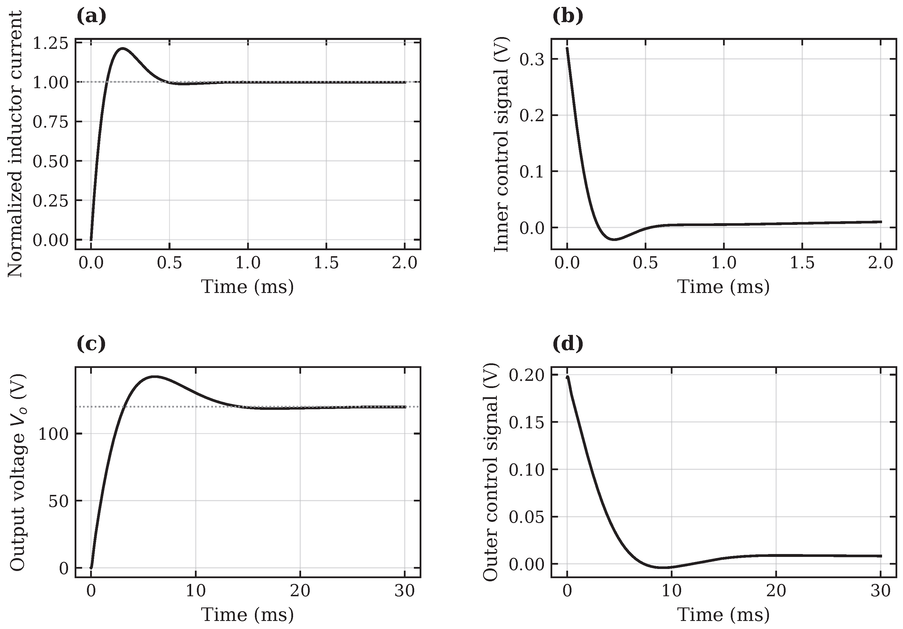
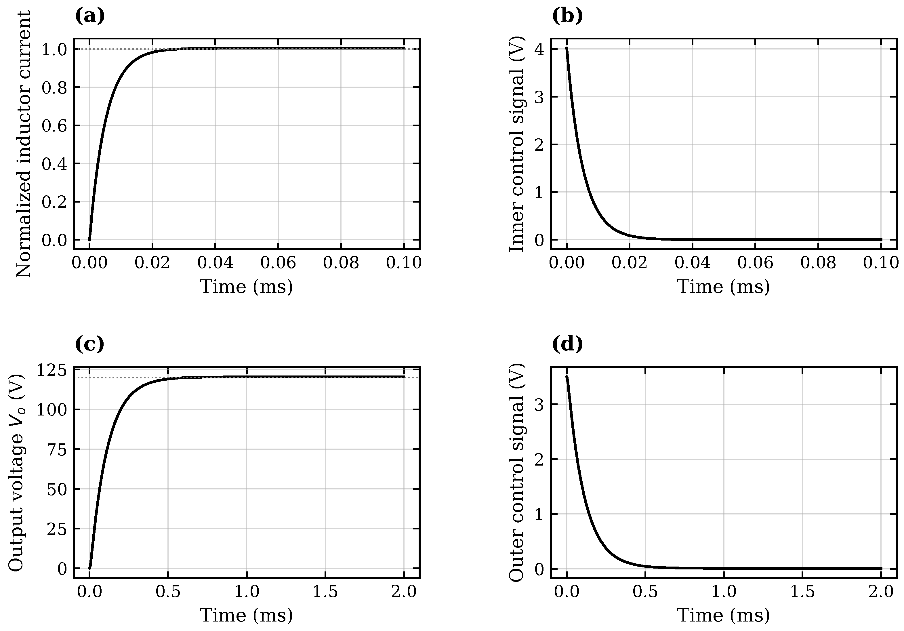
Figure 7 and Figure 8 show the simulated responses and control signals obtained with the proposed IO–LL and FO–LL controllers, respectively.
To complement the conventional transient-performance measures, the integral absolute error (IAE) and the integral squared control variation (ISU) were also calculated. To prevent these integral indices from depending on the small residual steady-state errors, they were evaluated with respect to the corresponding steady-state values as
IAE = ∫ 0 T f y ∞ − y ( t ) d t ,
and
ISU = ∫ 0 T f u ( t ) − u ∞ 2 d t .
For the inner and outer loops, respectively, the integration horizons were selected as
T f , i = 5   ms , T f , e = 100   ms .
Table 6 summarizes the quantitative nominal performance of the four controller structures. Since the unconstrained FO–PI produces particularly large control amplitudes, an additional case with an ideal ±5 V saturation applied at the FO–PI controller output, after the rational CFE realization and before the corresponding plant input, is included. This saturation represents a generic amplitude constraint rather than the nonlinear model of a specific electronic device.
The integer-order results show that IO–PI and IO–LL provide comparable settling times and control amplitudes in both loops, although the IO–PI exhibits lower overshoot and steady-state error. Thus, the analytically designed IO–LL achieves a response speed and control demand comparable to those of the integer-order PI benchmark.
A different tradeoff is observed for the fractional-order controllers. The unconstrained FO–PI provides the fastest nominal tracking, but requires control amplitudes far beyond those of the other controllers, reaching 724.3 V in the inner loop and 20.63 V in the outer loop. Imposing the ±5 V limit substantially reduces this demand while preserving a very fast response. In contrast, the FO–LL incorporates the initial control-signal constraint directly into the analytical synthesis and remains below the prescribed amplitude limit without requiring an external saturation element, with u max = 4  V and 3.5 V for the inner and outer loops, respectively. The resulting response is slower than that of the saturated FO–PI but requires lower overall control effort, as reflected by the ISU in both loops.
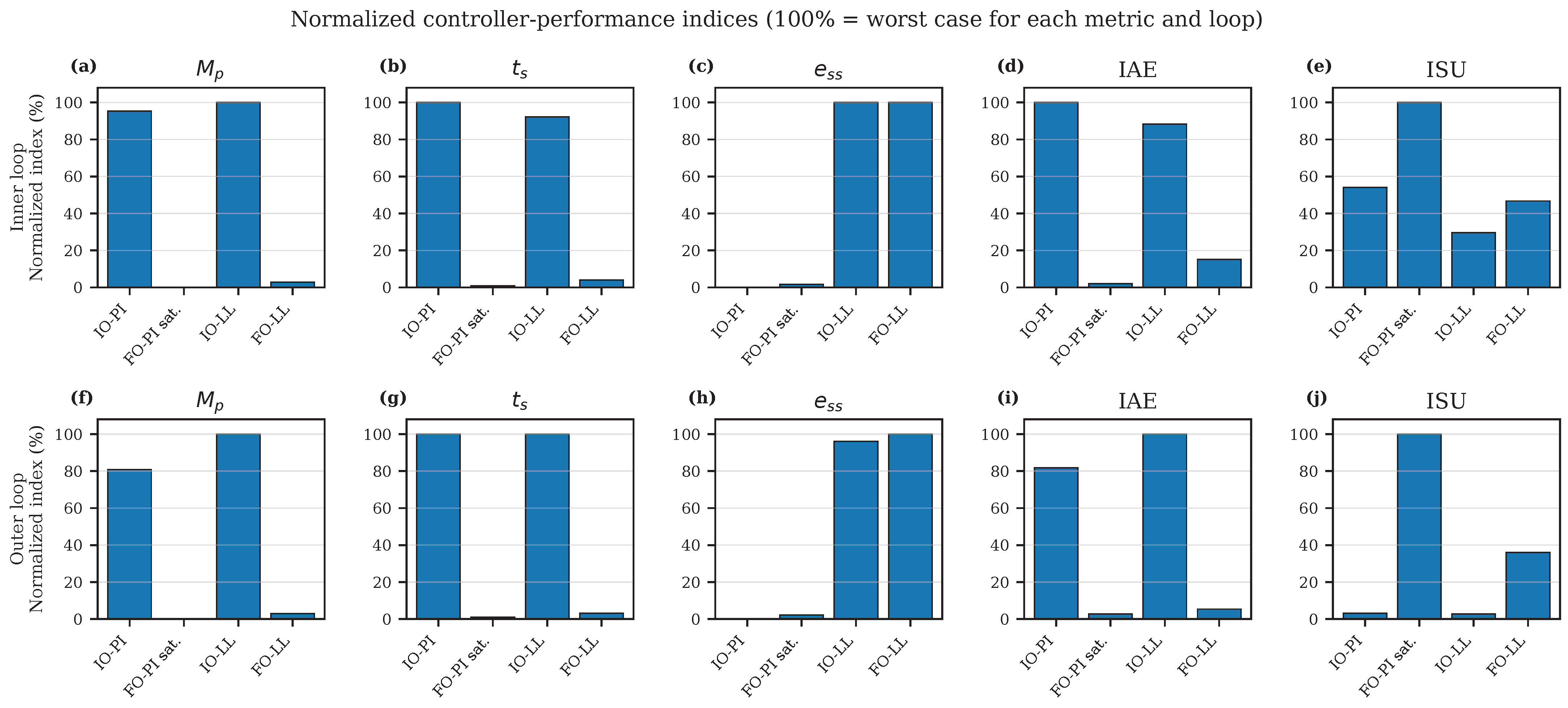
Figure 9 provides a complementary visualization of these tradeoffs, where 100% represents the least favorable value of each metric within the corresponding loop. The unconstrained FO–PI controller is intentionally excluded from this normalization because its extremely large control demand represents an unconstrained ideal benchmark rather than a practically amplitude-limited case. The saturated FO–PI generally provides the fastest tracking response, whereas the FO–LL provides a more balanced compromise between transient performance and control effort. The comparable settling times and control amplitudes of IO–PI and IO–LL are also evident.
No anti-windup compensation is included in the constrained FO–PI because the purpose of this case is to evaluate the original FO–PI design under the same finite control-amplitude limit considered for practical implementation. The saturation is applied only to the controller output; therefore, the internal states of the rational CFE approximation are neither clamped nor reset during saturation and continue to evolve according to the controller dynamics driven by the control error. No back-calculation or other feedback from the saturated output to the controller states is introduced. Consequently, state accumulation during saturation is permitted in this benchmark. Introducing an anti-windup scheme would add an additional control mechanism and modify the original benchmark, leading to a comparison with an augmented FO–PI architecture. Therefore, the constrained FO–PI is used to distinguish the effect of imposing the control-amplitude limit externally from incorporating the control-effort requirement directly into the analytical synthesis, as in the proposed FO–LL design.
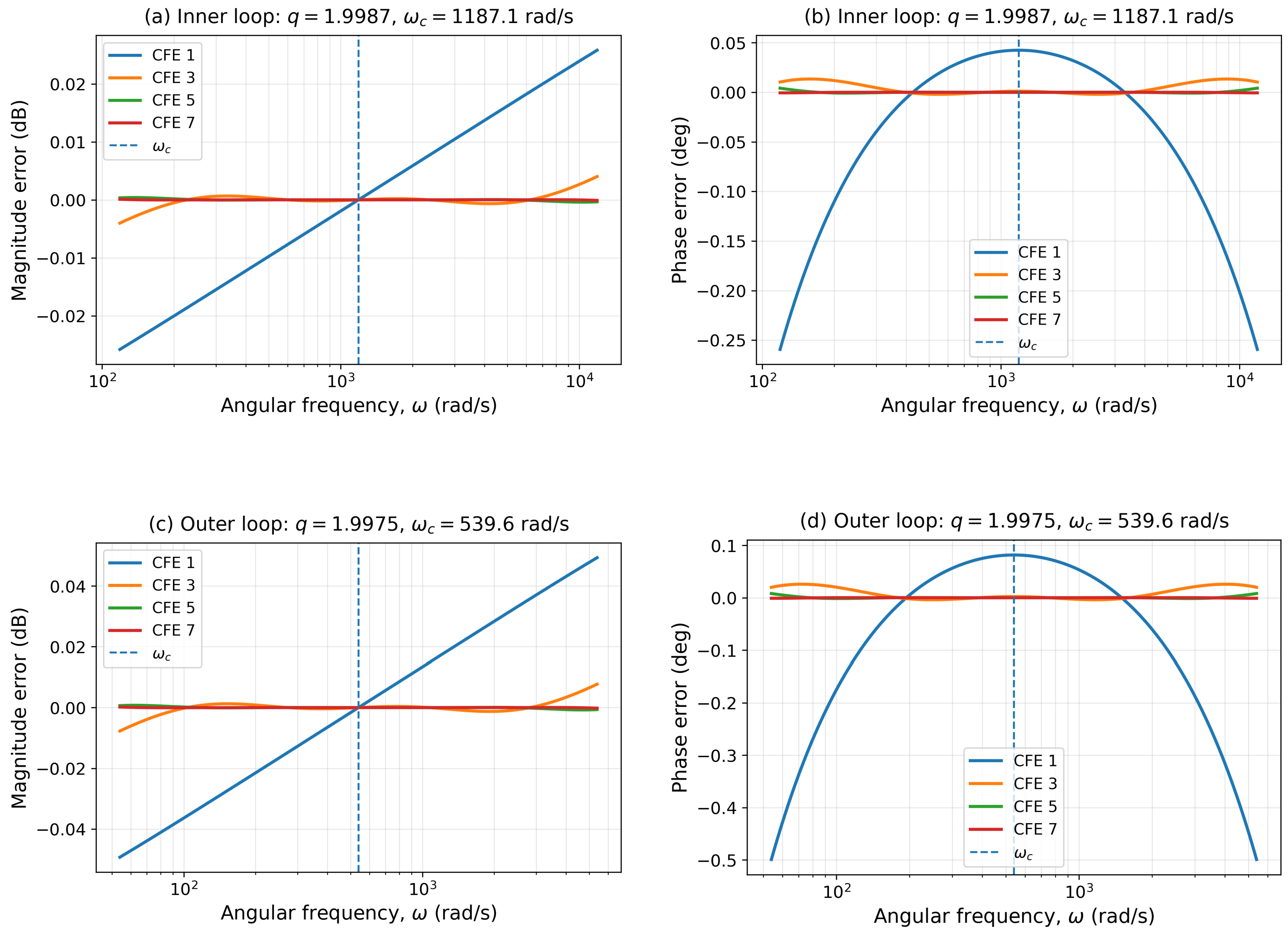
Before evaluating the effect of the rational-approximation order on the closed-loop response, the accuracy of the CFE approximation of the fractional operator s q was quantified in the frequency domain for the actual fractional orders obtained for the FO–LL controllers. For the inner loop, q i = 1.9987 , whereas for the outer loop, q e = 1.9975 . Since 1 < q < 2 , the fractional operator is expressed as s q = s s q ˜ , with q ˜ = q − 1 , and the CFE is applied to the fractional factor s q ˜ .
For this frequency-domain accuracy assessment, the CFE was additionally frequency-scaled about the corresponding design crossover frequency so that the approximation error could be evaluated over the frequency region relevant to each control loop. This frequency scaling is introduced only for the additional approximation-error analysis reported in Figure 10; the normalized CFE formulation described in Section 2.4.5 is the one used for the practical controller realization and for the closed-loop CFE-order simulations reported subsequently.
For the inner loop, the approximation was evaluated over 0.1 ω c , i ≤ ω ≤ 10 ω c , i , with ω c , i = 1187.1  rad/s, corresponding to 118.71 ≤ ω ≤ 11871  rad/s. For the outer loop, 0.1 ω c , e ≤ ω ≤ 10 ω c , e was considered, with ω c , e = 539.6  rad/s, corresponding to 53.96 ≤ ω ≤ 5396  rad/s.
The approximation errors decrease systematically as the CFE order increases. For the first-order CFE, the maximum magnitude and phase errors over these intervals are approximately 0.026 dB and 0.26° for the inner loop, and 0.049 dB and 0.50° for the outer loop. The corresponding RMS magnitude and phase errors are approximately 0.015 dB and 0.096° for the inner loop and 0.029 dB and 0.184° for the outer loop. Higher-order CFE approximations further reduce these errors.
Although frequency scaling substantially improves the operator-level approximation around the corresponding crossover frequency, the practical FO–LL implementation in this work was based on the normalized CFE formulation introduced in Section 2.4.5. Therefore, an additional closed-loop comparison was performed to determine whether the absence of frequency scaling in the implemented realization materially affects the resulting FO–LL performance.
Table 7 shows that frequency scaling has only a limited influence on the evaluated FO–LL closed-loop performance. For the inner loop, the variations in M p , t s , ISU, and u max are negligible. For the outer loop, the most noticeable difference occurs in the overshoot; however, it remains below 1% for both the normalized and frequency-scaled realizations. The settling time changes only slightly, whereas ISU and u max remain essentially unchanged. Thus, although frequency scaling improves the approximation of the fractional operator over the frequency region surrounding the crossover frequency, the principal closed-loop performance conclusions obtained with the normalized CFE realization used in the practical implementation are preserved.
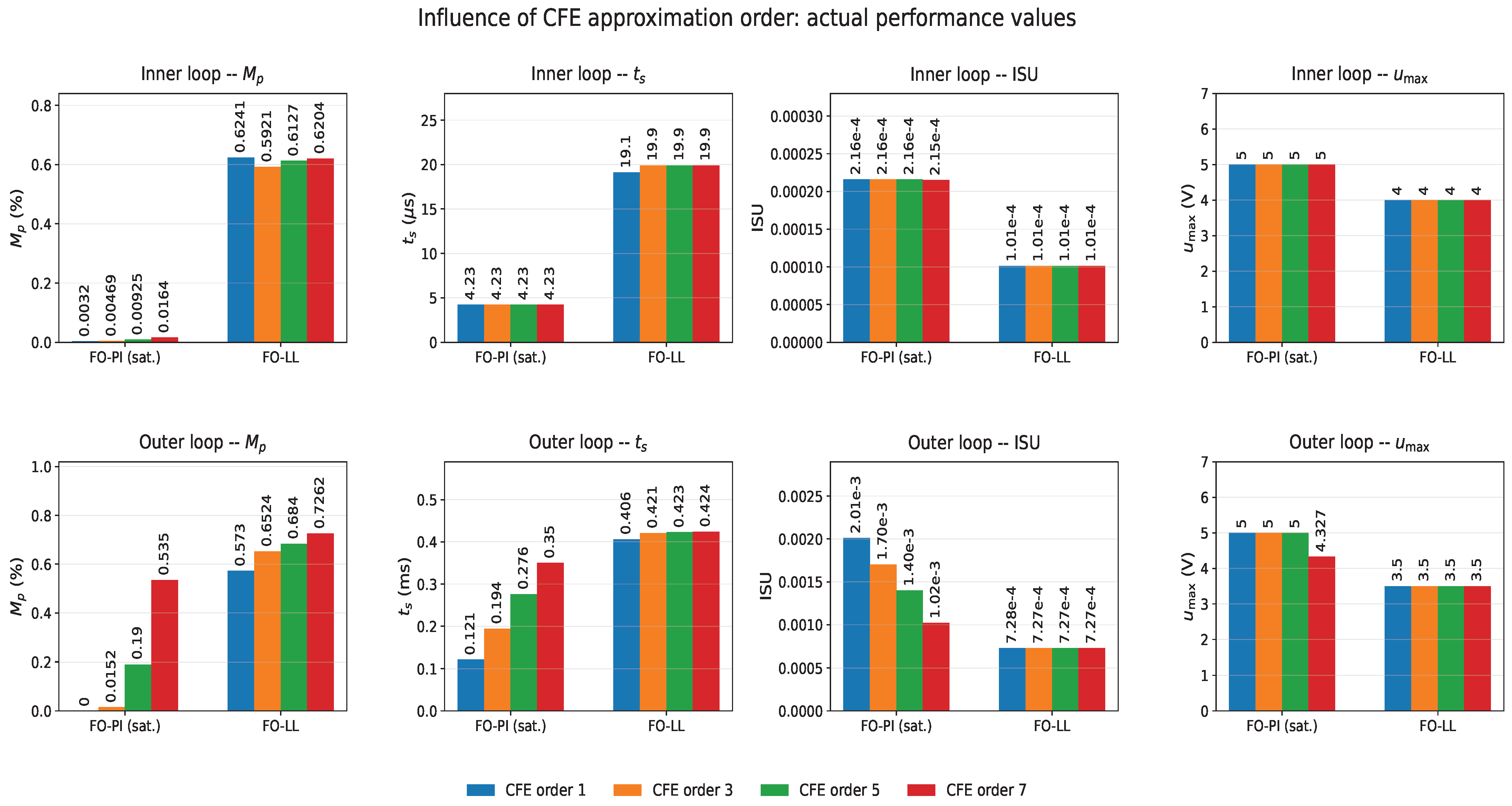
The influence of the CFE approximation order on the closed-loop response was then investigated using the normalized CFE formulation employed in the controller realization, considering first-, third-, fifth-, and seventh-order approximations. The FO–PI controller was evaluated with the ±5 V output limitation, whereas the FO–LL controller was evaluated without saturation because its nominal control signal remains within this range. Figure 11 compares the resulting overshoot, settling time, ISU, and maximum control-signal amplitude.
Figure 11 shows that the CFE approximation order has a limited influence on the FO–LL controller. For both loops, M p , t s , ISU, and u max remain within a narrow range from first- to seventh-order approximations. The constrained FO–PI is also weakly affected in the inner loop, where the ±5 V limit dominates the initial control action. In the outer loop, however, increasing the CFE order produces a slower response with lower ISU; moreover, the seventh-order approximation no longer reaches the saturation limit, with u max ≈ 4.33  V.
Overall, the constrained FO–PI exhibits a tradeoff between transient speed and control effort as the CFE order increases, particularly in the outer loop. In contrast, the FO–LL closed-loop response is only weakly affected by the CFE approximation order. The additional frequency-scaling analysis also shows that the FO–LL closed-loop performance obtained with the normalized realization remains close to that obtained when the CFE is scaled around the corresponding crossover frequency. These results support the use of the normalized first-order CFE adopted for the practical low-order realization, since the principal closed-loop performance conclusions are preserved while maintaining a low implementation complexity.

4.2. Reference Tracking and Input-Voltage Disturbance Rejection

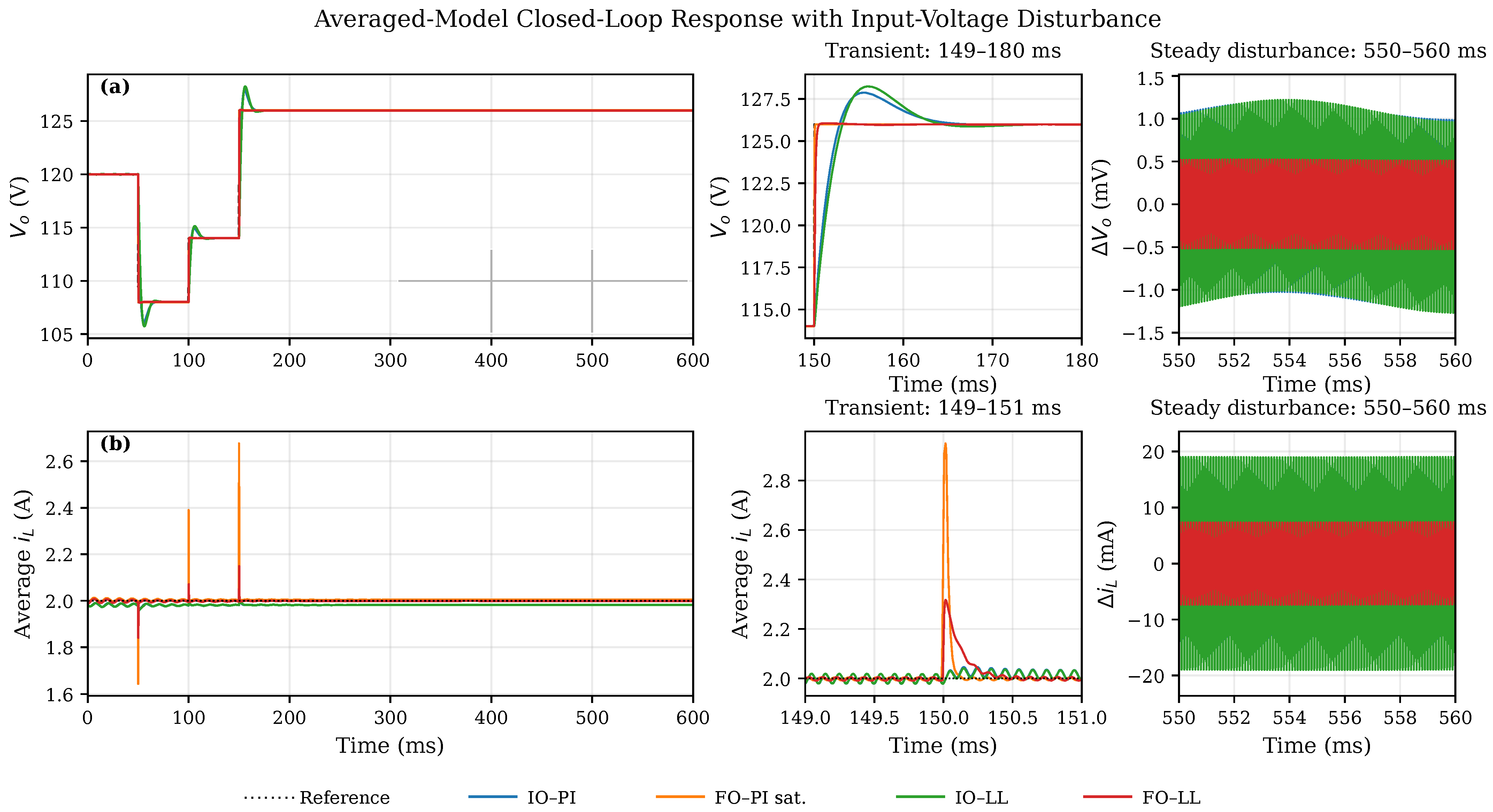
The four controllers were evaluated under simultaneous reference changes and input-voltage disturbances using the averaged small-signal model. Successive output-voltage references of 120 → 108 → 114 → 126 → 120  V were applied at t = 50 , 100, 150 ms, and 200 ms, respectively. Simultaneously, a 10 kHz sinusoidal input-voltage perturbation with an amplitude equal to 5% of the nominal input voltage, V i n = 60  V, was applied around the nominal operating point,
V g ( t ) = 3 sin 2 π 10 4 t V .
The disturbance was introduced through both G i L v g ( s ) and G v o v g ( s ) , thereby accounting for its effect on both the inner current and outer voltage dynamics. The ±5 V control-signal constraint was retained for the FO–PI controller.
Figure 12 shows the output-voltage and average inductor-current responses. All controllers maintain stable tracking for the evaluated reference changes in the presence of the input-voltage disturbance. The zoomed regions around t = 150  ms highlight the corresponding transients, whereas those between 550 and 560 ms show the residual steady-state oscillations after the reference transient has decayed.
Since the averaged model does not reproduce the 40 kHz PWM switching process, the oscillations observed in the steady-state zooms correspond exclusively to the residual effect of the imposed 10 kHz input-voltage disturbance and not to switching ripple. Their peak-to-peak values were measured directly over 550 ≤ t ≤ 560  ms, without additional filtering, as
Δ V o , pp = V o , max − V o , min , Δ i L , pp = i L , max − i L , min .
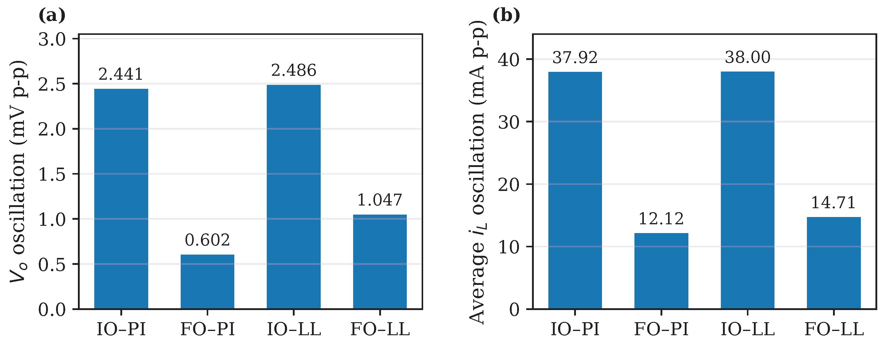
Figure 13 summarizes the residual peak-to-peak output-voltage and average-inductor-current oscillations produced by the 10 kHz input-voltage disturbance.
For the imposed 10 kHz input-voltage disturbance, the fractional-order controllers provide stronger attenuation than their corresponding integer-order counterparts. FO–PI reduces the output-voltage and inductor-current oscillations by 75.3% and 68.0%, respectively, relative to IO–PI, whereas FO–LL achieves reductions of 57.9% and 61.3% relative to IO–LL. Thus, under the evaluated disturbance condition, the fractional-order implementations maintain stable reference tracking while providing improved disturbance rejection at both the regulated output and the inner current loop.

4.3. Performance at Different Duty-Cycle Operating Points

The proposed IO–LL and FO–LL controllers, designed at the nominal operating point D = 0.5 , were kept fixed and subsequently evaluated at D = { 0.40 , 0.45 , 0.50 , 0.55 , 0.60 } . For V i n = 60  V, the corresponding operating-point voltages, obtained from V o 0 = V i n / ( 1 − D ) , are V o 0 = { 100 , 109.09 , 120 , 133.33 , 150 }  V. For each value of D, the averaged small-signal converter model was recalculated without retuning either controller.
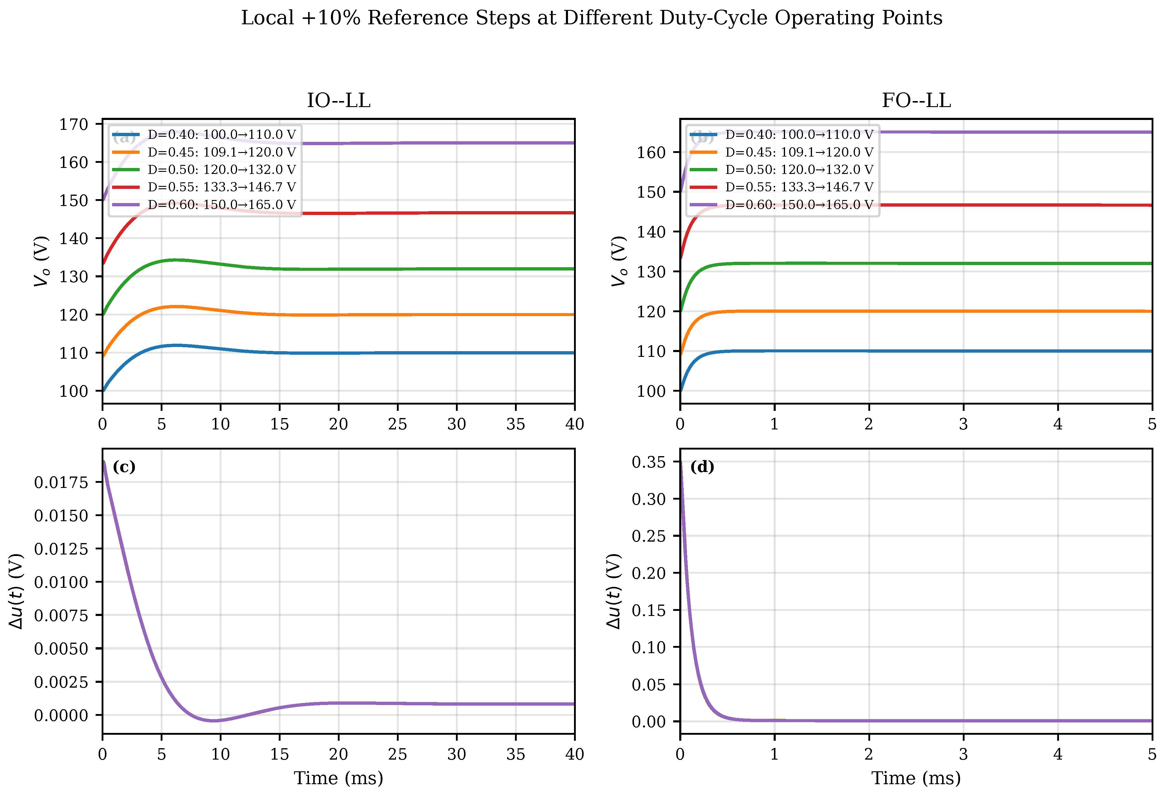
Since each small-signal model describes the converter dynamics around its corresponding operating point, a +10% reference step was applied around each V o 0 . The resulting transitions were 100 → 110 , 109.09 → 120 , 120 → 132 , 133.33 → 146.67 , and 150 → 165  V. Figure 14 shows the resulting output-voltage responses and incremental control signals, whereas Table 8 summarizes the corresponding M p , t s , e s s , and maximum incremental control action Δ u max .
The results show that both controllers preserve essentially the same closed-loop behavior throughout the evaluated duty-cycle range without retuning. For IO–LL, the variations in M p , t s , and e s s are negligible, while Δ u max remains approximately 0.0190  V. Similarly, FO–LL maintains M p < 0.6 % , t s < 0.41  ms, and e s s ≈ 0.21 % , with Δ u max ≈ 0.35  V at all operating points. The closed inner current loop therefore contributes to reducing the sensitivity of the effective outer-loop dynamics to changes in the duty-cycle operating point over the evaluated range.
For the FO–LL controller, the approximately 0.35 V maximum incremental control action produced by the +10% reference step is consistent with the prescribed u 0 = 3.5  V for a unit normalized reference change.

4.4. Robustness to Converter Parameter Variations

The robustness of the IO–LL and FO–LL controllers to converter-parameter variations was evaluated through a Monte Carlo analysis with N = 1000 realizations. The controllers were kept fixed at their nominal design values, while L, C, and R were independently varied according to uniform distributions within ±20% of their nominal values. The nominal operating point was maintained at D = 0.5 , V i n = 60  V, and V o 0 = 120  V, and a local +10% reference step ( 120 → 132  V) was applied in every realization.
Figure 15 shows the output-voltage and incremental control-signal responses. The shaded regions represent the pointwise 95% intervals obtained from the Monte Carlo realizations, together with the corresponding mean and nominal responses. All 1000 realizations remained stable for both controllers.
Table 9 summarizes the resulting performance indices and the corresponding compliance probabilities. The IO–LL controller exhibits mean values of M p and t s close to their nominal values, with standard deviations corresponding to approximately 7.2% and 4.8% of their respective means. For FO–LL, the corresponding relative dispersions are approximately 11.8% and 11.3%; however, the resulting overshoot and settling-time values remain small in absolute terms. The relative dispersion of e s s is similar for both controllers, approximately 12%, while the maximum incremental control action is practically unaffected by the converter-parameter variations. Both controllers remain stable throughout the considered uncertainty range without controller retuning.
The compliance results distinguish between the original outer-loop specifications and preservation of the achieved nominal performance. FO–LL essentially preserves the original M p and t s requirements, whereas IO–LL does not, since its nominal complete cascade already exhibits approximately 19% overshoot and 13 ms settling time. Nevertheless, when a maximum 20% degradation relative to the achieved nominal performance is adopted as a robustness criterion, both controllers exhibit high performance-preservation probabilities. The lower compliance with the original e s s ≤ 0.2 % requirement is explained by the nominal steady-state errors lying very close to this limit.

4.5. Robustness to Controller-Component Tolerances

The robustness of the analog IO–LL and FO–LL implementations was evaluated through a Monte Carlo analysis with N = 1000 realizations. Every physical resistor and capacitor in the inner- and outer-loop controller circuits was independently varied using uniform distributions, with tolerances of ±5% for resistors and ±10% for capacitors, without assuming matched components. The nominal component values are those reported in Table 5. The converter parameters were kept at their nominal values, and a local reference step from 120 to 132 V was applied.
Figure 16 shows the resulting output-voltage and control-signal responses. The shaded regions represent the 95% intervals, while the nominal and Monte Carlo mean responses are also shown. All 1000 realizations remained stable for both controller implementations.
The transient-response indices remain relatively concentrated despite the independent component variations. For IO–LL, M p = 19.39 ± 1.55 % and t s = 13.27 ± 1.37  ms, whereas FO–LL yields M p = 0.565 ± 0.183 % and t s = 0.409 ± 0.018  ms. In contrast, the steady-state error is more sensitive to component mismatch, with mean values of 3.996% and 1.072% for IO–LL and FO–LL, respectively.
This sensitivity is mainly associated with resistor-ratio mismatch in the differential and summing stages. When only these resistor tolerances were reduced from ±5% to ±1%, the maximum e s s decreased from 16.95% to 3.17% for IO–LL and from 4.00% to 0.98% for FO–LL. These results indicate that resistor matching in the differential and summing stages plays a dominant role in the steady-state accuracy of the implemented controllers.
Temperature drift was not modeled separately because its quantitative evaluation would require the temperature coefficients and operating-temperature profiles of the specific components. Nevertheless, its principal effect on the passive controller network is reflected in variations of the effective resistor and capacitor values, whose influence is already assessed by the component-tolerance analysis. A dedicated thermal characterization of the analog implementation is therefore beyond the scope of this work.

4.6. Load-Step Disturbance Rejection

The load-disturbance rejection of the IO–LL and FO–LL controllers was evaluated with the controllers fixed at their nominal design values and the output-voltage reference maintained at V ref = 120  V. The load resistance was changed according to
120 → 96 → 144 → 120   Ω
at t = 50 , 100, and 150 ms, respectively.
Since the analysis is based on averaged small-signal models, the converter model was recalculated for each value of R. The simulation was performed piecewise by switching to the corresponding linearized model at each load transition while preserving the inductor-current, output-voltage, and controller states. Thus, neither the plant nor the controllers were reinitialized, allowing the transient evolution between successive operating conditions to be evaluated continuously.
Figure 17 shows the load profile and the corresponding output-voltage, average inductor-current, and capacitor-current responses. The capacitor current was obtained consistently from the averaged model as
i C ( t ) = C d v o ( t ) d t .
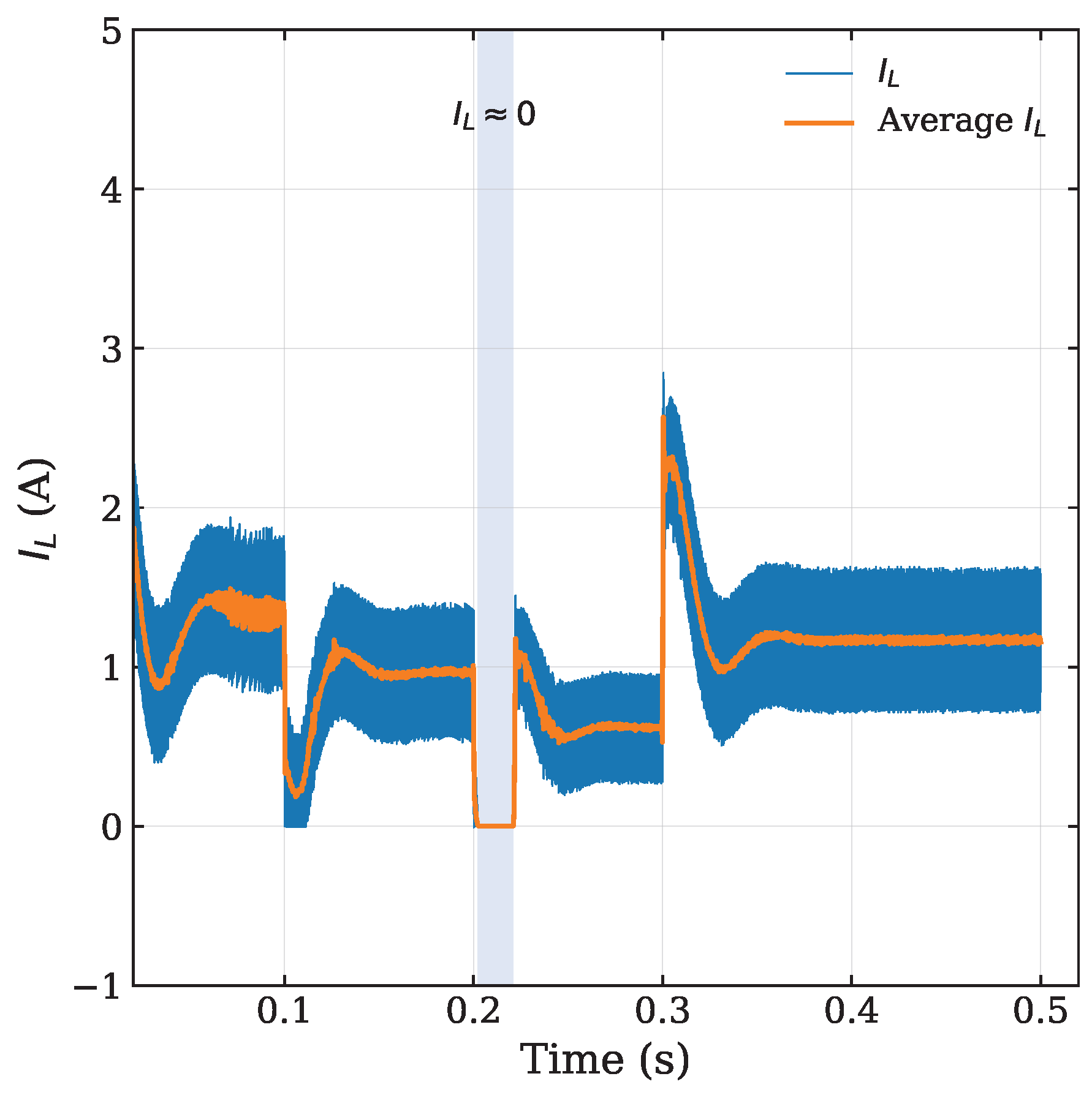
At each load transition, the inductor current remains continuous and evolves toward the value required by the new load, whereas the capacitor supplies or absorbs the instantaneous current imbalance, with i C subsequently returning toward zero.
Both controllers maintain stable voltage regulation throughout the load sequence. For the 120 → 96 , 96 → 144 , and 144 → 120   Ω transitions, the maximum absolute output-voltage deviations from the 120-V reference are 0.797, 1.282, and 0.494 V for IO–LL, respectively, and 0.069, 0.062, and 0.042 V for FO–LL.
To quantify disturbance rejection independently of the small steady-state offset, the recovery time was evaluated with respect to the post-disturbance steady-state voltage. For each load transition, Δ V o , tr was defined as the maximum transient deviation from the corresponding post-disturbance steady-state value, and t r as the time required for the output-voltage deviation to enter and remain within 2% of Δ V o , tr . The corresponding recovery times are approximately 19.1 ms for IO–LL and 7.9 ms for FO–LL for all three load transitions.
Therefore, both controllers reject the considered load variations without retuning, while FO–LL exhibits substantially smaller output-voltage excursions and faster disturbance recovery.

5. Circuit-Level Simulation and Experimental Validation

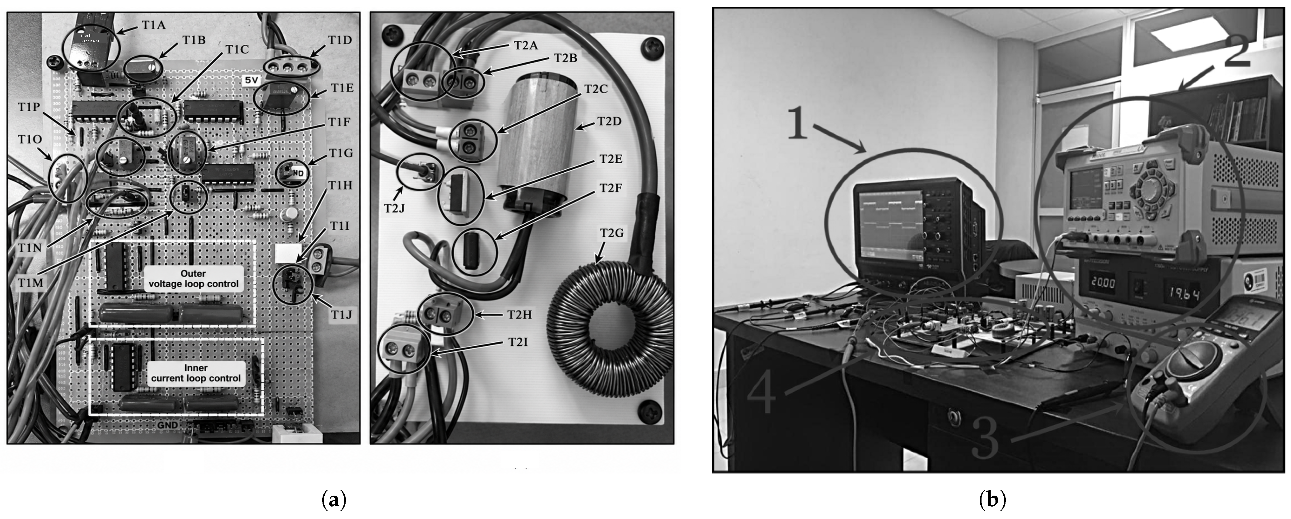
To complement the comparative evaluation presented in Section 4, the proposed methodology was applied to a second Boost converter intended for experimental implementation. The prototype operates with V i n = 20  V and a nominal output voltage of V o = 46  V, with R = 116   Ω , L = 0.7  mH, C = 470  µF, and a switching frequency of f = 20  kHz. The nominal duty cycle is D = 0.565 . For this implementation, the cascade architecture combines an IO–LL controller in the inner current loop and an FO–LL controller in the outer voltage loop.
For this hybrid IO–LL/FO–LL configuration, validation is performed at three successive levels: block-level verification using the averaged small-signal model, circuit-level simulation using the switching Simulink/Simscape model, and experimental evaluation using the physical prototype. The controller parameters obtained from the analytical design are retained throughout these stages, enabling a progressive assessment of the design as increasing implementation detail is introduced.

5.1. Automated Controller Design and Block-Level Verification

The controllers were synthesized using the automated procedure described in Section 3.1.4 and implemented in dc_dc_lead_lag.m. The resulting closed-loop system was first evaluated at block level using the averaged small-signal model. The controller parameters and analog component values obtained at this stage were retained for the subsequent circuit-level and experimental validation.
For the inner current loop, the prescribed design specifications were M p = 5 % , t s = 0.5  ms, and e s s < 0.15 % (design value: e s s = 0.1435 % ). The resulting IO–LL controller is
G c i ( s ) = 0.02957 s + 166 0.18179 s + 1 .
After closing the inner current loop, the resulting effective plant K L I ( s ) is used for the outer-loop synthesis. For the outer voltage loop, M p = 5 % , t s = 25  ms, and e s s < 0.15 % were specified, together with a control-effort specification of u 0 , e = 5  V. The resulting fractional-order parameters are K e x t = 198 , q e = 1.1286 , α e = 0.02525 , and τ e = 0.15377  s.
Using the first-order CFE adopted for the electronic realization, the ideal fractional-order outer controller is approximated by
G c v f ( s ) ≈ 5.000 s 2 + 997.97 s + 1287.61 s 2 + 5.7928 s + 6.5031 .
The practical component values selected for the circuit implementation are reported in Table 10.
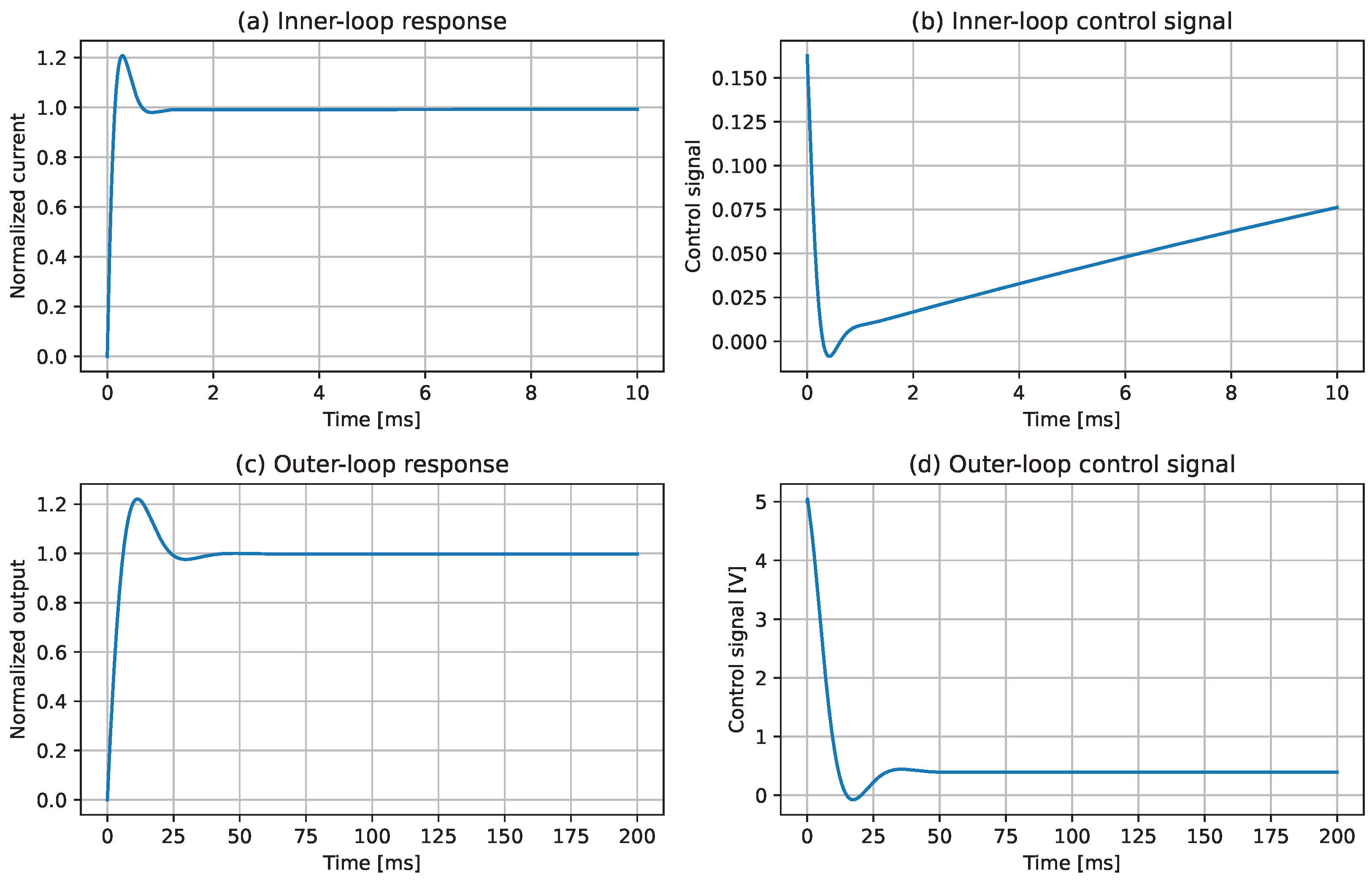
The block-level closed-loop responses obtained from the averaged small-signal model are shown in Figure 18. The inner-loop response gives M p = 20.81 % and t s = 0.885  ms. For the complete cascade system, M p = 22.12 % , t s = 33.06  ms, and e s s = 0.200 % are obtained, with a maximum outer-loop control signal of approximately 5.05 V.
The simulated overshoot is higher than the prescribed 5% value for both loops. This discrepancy can be attributed, at least in part, to evaluating the actual interconnected closed-loop system rather than the second-order reference model used to derive the frequency-domain design specifications. Consequently, the prescribed overshoot should be interpreted as a design target associated with the reference-model-based synthesis rather than as an exact performance constraint on the complete interconnected system. The resulting responses nevertheless provide the baseline block-level behavior against which the subsequent circuit-level and experimental implementations are evaluated. In addition, the maximum outer-loop control signal of approximately 5.05 V closely agrees with the prescribed control-effort specification u 0 , e = 5  V, showing that this additional design requirement is effectively reflected in the resulting FO–LL controller.

5.2. Circuit-Level Simulation

The hybrid IO–LL/FO–LL cascade controller was subsequently evaluated using the switching circuit model implemented in dc_dc_lead_lag.slx. Unlike the averaged small-signal model used for block-level verification, the Simulink/Simscape implementation incorporates the switching power stage and the electronic controller realizations using the selected commercial component values. This model therefore provides an intermediate validation stage between the averaged analytical representation and the physical prototype.
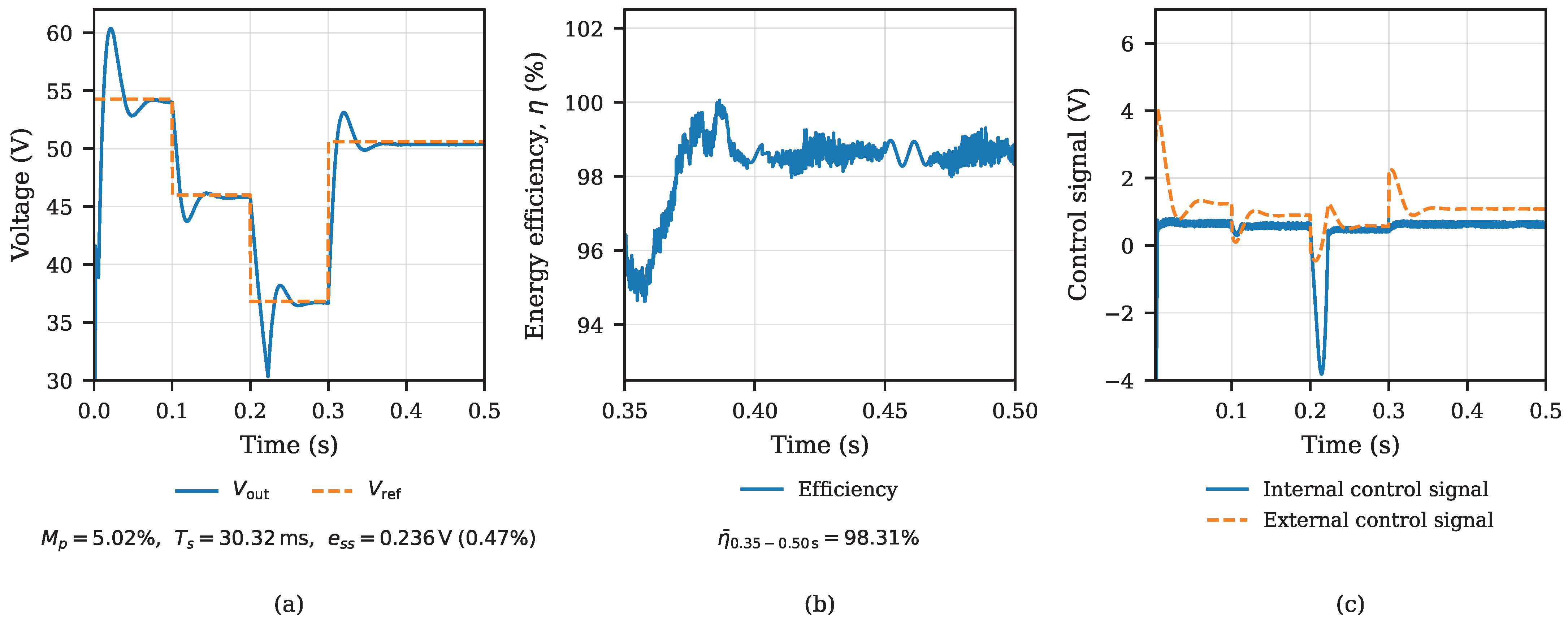
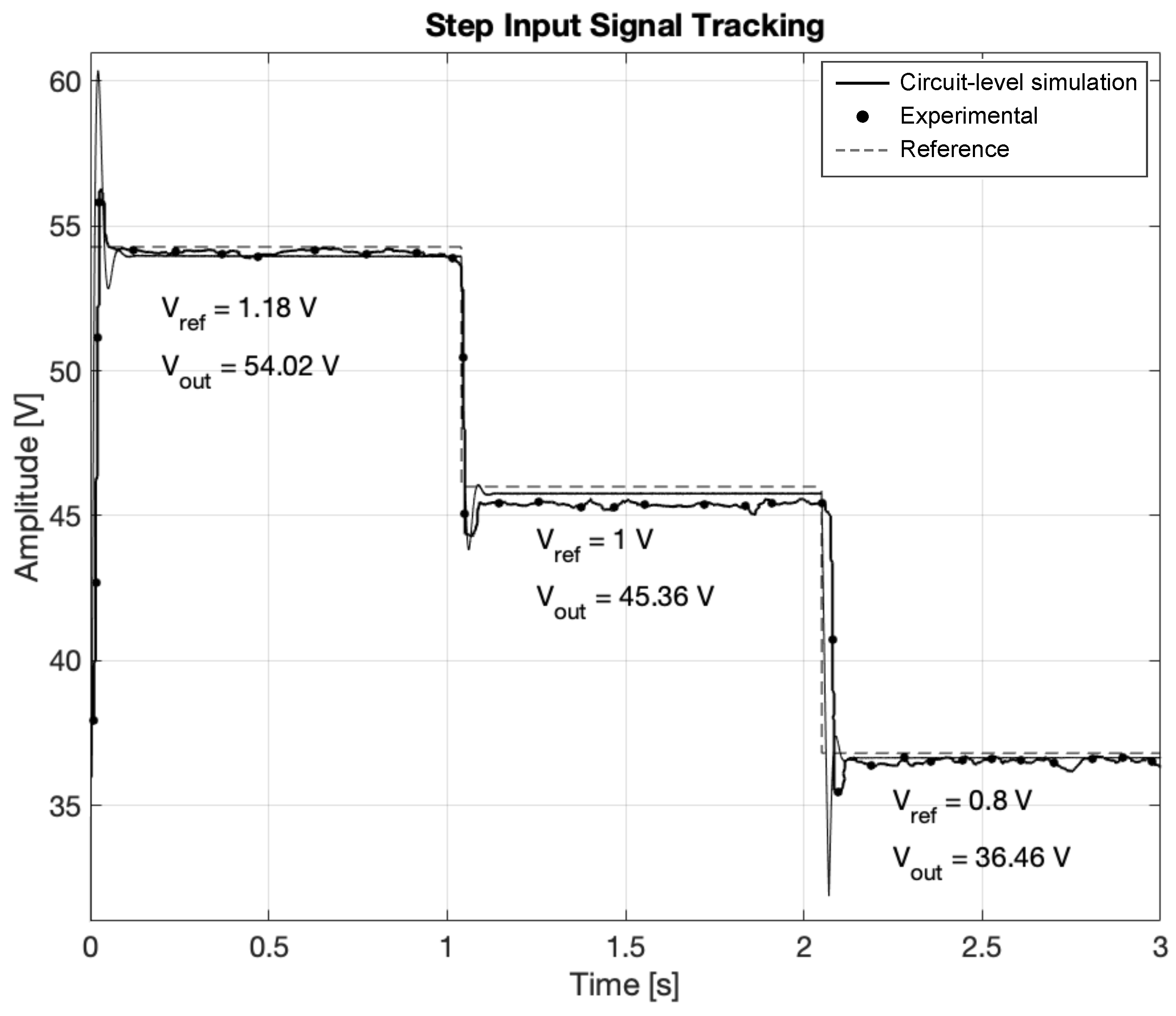
Figure 19a shows the circuit-level output-voltage response under successive reference changes. The converter tracks both upward and downward changes while maintaining stable closed-loop operation with the controller parameters obtained from the analytical design. For the final reference transition, from approximately 36.5 to 50.5 V, the response yields M p = 5.02 % , t s = 30.32  ms, and e s s = 0.236  V (0.47%). Compared with the block-level response, for which M p = 22.12 % , t s = 33.06  ms, and e s s = 0.20 % , the switching circuit model preserves essentially the same settling-time scale and a small steady-state error, while exhibiting a substantially lower overshoot. Because the reference transitions and operating ranges are not identical, the difference in overshoot cannot be attributed solely to model fidelity. It may also be influenced by the range over which the block-level response was evaluated. In that analysis, the output-voltage response spans approximately 0–60 V, whereas the averaged small-signal model is obtained by linearization around the nominal operating point and is therefore intended to represent local perturbations. Such a large excursion may exceed the range over which the linearized model accurately represents the nonlinear Boost-converter dynamics. In contrast, the circuit-level switching model directly represents the converter operation over the complete voltage excursion. Therefore, the reduction from 22.12% to 5.02% should not be interpreted solely as an implementation-induced damping effect, but may also reflect both the different test conditions and the limitations of applying the small-signal block-level model to a large-signal transient.
Figure 19b shows the conversion efficiency after the final reference transition. Over the 0.35–0.50 s interval, the mean simulated efficiency is 98.31%. The remaining ripple is associated with the switching operation and the instantaneous power quantities used to compute the efficiency. This result provides a circuit-level estimate of the power-conversion performance that is not represented by the averaged small-signal closed-loop model.
Figure 19c shows the inner- and outer-loop control signals throughout the complete reference sequence. Both signals remain bounded despite the successive operating-point changes. In particular, the outer-loop control signal remains consistent with the u 0 , e = 5  V control-effort specification, while the inner-loop signal exhibits its largest excursion during the most demanding downward transition and subsequently returns to its nominal operating range. These results show that the hybrid cascade controller preserves stable operation over the evaluated reference sequence without controller retuning.
Figure 20 reports the inductor current i L obtained from the switching circuit-level simulation, including both the instantaneous waveform associated with the 20 kHz PWM operation and its filtered average value. The instantaneous current exhibits the switching-frequency ripple, whereas the average current highlights the slower dynamics imposed by the cascade control system. During the highlighted interval, i L reaches zero and remains at zero for a finite portion of the transient, indicating a temporary transition from continuous-conduction mode (CCM) to discontinuous-conduction mode (DCM). This behavior occurs when the large-signal transient drives the converter across the CCM–DCM boundary and, consequently, outside the validity region of the CCM small-signal model used for controller synthesis. The observed temporary transition to DCM therefore illustrates the nonlinear large-signal behavior captured by the switching circuit-level model and provides additional information beyond that obtainable from the CCM small-signal representation.
The finite bandwidth and slew-rate limitations of the operational amplifiers were neglected in the circuit-level simulation because the characteristic controller dynamics are well below the corresponding device limits. For the inner-loop controller, the pole is located at approximately 5.51   rad / s , whereas its zero is at 5.63 × 10 3   rad / s (≈896 Hz). The outer-loop controller exhibits even slower dynamics, with poles at approximately 1.52 and 4.27   rad / s and zeros at 1.30 and 198.5   rad / s . The highest of these characteristic frequencies is therefore approximately 896 Hz, more than three orders of magnitude below the typical 3 MHz gain-bandwidth product of the TL084 operational amplifiers used in the experimental implementation. Moreover, the TL084 exhibits a typical slew rate of approximately 13   V / μ s , corresponding to an ideal slew-limited transition time of only about 0.385   μ s for a 5 V output excursion, whereas the relevant closed-loop transients evolve on a millisecond time scale. Consequently, neither finite gain bandwidth nor slew rate is expected to have a noticeable influence on the reported closed-loop response, and these nonidealities were not explicitly included in the circuit-level model.

5.3. Electronic Implementation and Experimental Setup

The controller circuits were implemented using the practical component values reported in Table 10 and TL084 operational amplifiers supplied at ±5 V.
The inner-loop feedback current is obtained using an ACS712 Hall-effect current sensor with a sensitivity of 0.185 V/A and a zero-current output voltage of 2.5 V. Its output is processed by a conditioning stage with R s = 10  k Ω and R f = 54  k Ω , corresponding to a gain of R f / R s = 5.4 . The resulting incremental current-feedback gain is therefore 0.185 × 5.4 = 0.999  V/A, which is approximated as unity in the small-signal model. The dc offset is removed by the conditioning stage and does not affect the incremental current-feedback signal used by the inner IO–LL controller.
For the outer voltage loop, the output voltage is scaled by the R D 1 – R D 2 resistor network before being applied to the FO–LL controller. With R D 1 = 121.5  k Ω and R D 2 = 2.7  k Ω , the resulting scaling factor is R D 2 / ( R D 1 + R D 2 ) = 0.02174 , such that the nominal converter output of 46 V corresponds to a feedback voltage of approximately 1.00  V.
Figure 21 shows the implemented controller board, Boost converter, and experimental setup. The power stage and controller were constructed as separate boards, facilitating access to the relevant electrical variables during testing. Under the nominal experimental conditions, the converter operates in continuous-conduction mode, while the selected output capacitance limits the output-voltage ripple.
Experimental characterization was performed using the setup shown in Figure 21b. The experimental tests used the same hybrid IO–LL/FO–LL cascade architecture and controller parameters considered in the block-level and circuit-level evaluations, allowing the three validation levels to be assessed using the same controller configuration.

5.4. Experimental Results and Three-Level Validation

Figure 22 shows the experimental output-voltage response under successive reference changes. Reference voltages of 1.18 , 1.00 , and 0.80  V correspond to converter output voltages of approximately 54.02 , 45.36 , and 36.46  V, respectively.
The experimental response confirms stable tracking for both upward and downward reference changes around the nominal 46 V operating point. The same IO–LL inner controller and FO–LL outer controller are retained throughout the complete reference sequence, without gain scheduling or controller retuning. For the reference transition from 54.02 to 45.36  V, which brings the converter close to the nominal 46 V operating point, the experimental response yields M p = 4.2 % , t s = 40  ms, and e s s = 1 % . The maximum outer-loop control voltage is approximately 5 V, while the measured conversion efficiency is 91 % . In addition to validating the nominal design, the ability to regulate the output at approximately 36.46 , 45.36 , and 54.02  V demonstrates that the implemented cascade controller retains stable regulation over the evaluated operating range.
Table 11 summarizes the representative performance obtained at the block, circuit, and experimental validation levels. Because the reported metrics correspond to the characteristic transients evaluated at each level rather than to identical reference transitions, the comparison is intended to assess the consistency of the overall closed-loop behavior rather than provide a point-by-point reproduction of the same transient. The three levels represent a progressive transition from the averaged small-signal description used for analytical verification, through the switching circuit and electronic realization, to the physical prototype, while retaining the controller parameters obtained from the analytical design.
The three-level comparison shows that the principal closed-loop characteristics are preserved as increasing implementation detail is introduced. The circuit-level and experimental results exhibit a similar transient time scale and comparable representative overshoot values under their respective test conditions, whereas the block-level averaged model provides a more conservative overshoot prediction. As discussed in Section 5.2, the larger block-level overshoot may be partly associated with the limitations of the averaged small-signal model under the large output-voltage excursion considered.
The control-effort results remain consistent with the analytical design specification. The outer FO–LL controller was synthesized using u 0 , e = 5  V as the prescribed control-effort specification, and the resulting maximum outer-loop control signals remain close to this design value at all three validation levels. Likewise, the circuit-level and experimental efficiencies remain high, with the lower experimental value reflecting losses present in the physical converter that are not fully represented in the circuit-level model.
Overall, the results confirm that the analytically synthesized hybrid IO–LL/FO–LL controller can be transferred from the averaged model to the switching circuit and finally to the physical prototype without retuning. The consistency observed between the circuit-level and experimental results under their respective test conditions, together with stable tracking over multiple output-voltage references, supports the practical validity of the proposed design and implementation procedure.

6. Discussion

From a broader perspective, the results address several of the limitations identified in the state-of-the-art analysis. Previous studies generally focus on specific aspects of DC–DC converter control, whereas approaches that jointly integrate transient specifications, analytical design, fractional-order control, explicit consideration of control effort, and a complete validation path up to experimental implementation remain limited. The proposed methodology brings these elements together within a unified specification-driven framework, without requiring optimization procedures to determine the controller parameters. In addition, computational tools are provided to reproduce the controller design and block-level simulations, as well as the circuit-level validation, facilitating verification and reuse of the methodology. Therefore, the contribution lies not only in the performance of a particular controller, but also in establishing a reproducible link between design specifications, analytical synthesis, simulation, and practical implementation.
The sensitivity and robustness evaluations show that the proposed design is not restricted to nominal conditions. Stable operation and acceptable performance are maintained under changes in the fractional approximation order, operation away from the nominal point, converter-parameter variations, controller-component tolerances, and load disturbances. This is particularly relevant for fractional-order controllers, whose practical realization necessarily involves finite-order approximations and components subject to tolerances. Overall, these tests support the robustness of the analytical design against the principal modeling, operating, and implementation uncertainties considered.
The three-level validation of the hybrid IO–LL/FO–LL cascade configuration further demonstrates the transition from analytical synthesis to physical implementation. The averaged small-signal model provides a suitable basis for analytical design and block-level verification, whereas the switching circuit model captures additional large-signal and switching effects that are not represented by the averaged model. Despite these modeling differences, the same analytically obtained controller parameters are transferred from the averaged model to the switching circuit and ultimately to the physical prototype without retuning, while maintaining stable regulation and a control effort close to the prescribed value. This result also emphasizes the complementary roles of the three validation levels rather than requiring the averaged model to reproduce all implementation effects observed in the switching circuit and experimental prototype.
Within this general framework, the FO–LL controller provides the additional capability of explicitly incorporating control effort as a design specification together with the transient-performance requirements. Unlike the FO–PI with ideal saturation, where the control-signal amplitude is bounded through an external constraint, the FO–LL control-effort level is established as part of the analytical synthesis itself, providing a practical advantage for implementation. Although the present formulation and validation are limited to Boost converters operating in CCM, the underlying specification-driven methodology is not inherently restricted to this topology or conduction mode. Extension to other conduction modes, such as Discontinuous Conduction Mode (DCM), would require rederiving the corresponding steady-state relationships and dynamic models before applying the analytical controller-synthesis procedure. Similarly, the methodology could, in principle, be extended to other DC–DC converter topologies, such as Buck, Buck–Boost, Cuk, SEPIC, and Zeta converters, by deriving the corresponding topology-specific models and adapting the analytical synthesis equations to their particular dynamics. Validation of these extensions to other conduction modes and converter topologies constitutes a relevant direction for future work.

7. Conclusions

This paper presented an integrated specification-driven methodology for the analytical design and practical implementation of cascade-controlled Boost DC–DC converters. The proposed framework establishes a direct connection between converter specifications, power-stage sizing, averaged small-signal modeling, analytical controller synthesis, rational approximation of fractional-order dynamics, electronic realization, and experimental implementation. Unlike empirical, heuristic, or optimization-based approaches, the controller parameters are obtained analytically from the prescribed performance requirements, providing a systematic and reproducible design procedure.
The numerical evaluation showed that the resulting controllers maintain stable operation and acceptable performance beyond the nominal design conditions. The sensitivity studies considered the order of the fractional approximation, operation away from the nominal point, converter-parameter variations, controller-component tolerances, and load disturbances. These results indicate that the analytical design is not critically dependent on a particular approximation order or on exact nominal parameter values, which is especially relevant for the practical realization of fractional-order controllers.
For the hybrid IO–LL/FO–LL cascade configuration, the transition from analytical design to physical implementation was further assessed through block-level, switching circuit-level, and experimental validation. The same analytically obtained controller parameters were transferred through these three levels without retuning. Although the averaged small-signal model provides a conservative prediction of the overshoot for the large voltage excursion considered, the circuit-level and experimental evaluations exhibit consistent transient behavior under their respective test conditions. Representative overshoots of approximately 5.02% and 4.2% were obtained in the circuit-level and experimental evaluations, respectively; these values correspond to different reference transitions and are therefore not intended as a direct point-by-point comparison. The settling times nevertheless remain within the same characteristic time scale, and the steady-state error remains at or below 1%. The experimental converter also achieved an efficiency of approximately 91% and maintained stable voltage regulation over multiple reference conditions.
Within this general methodology, the fractional-order lead–lag controller provides an additional design capability by incorporating the control-effort level directly into the analytical synthesis. For the outer loop, the prescribed value of u 0 , e = 5  V remained representative from the analytical design through circuit-level simulation and experimental implementation. This differs fundamentally from imposing an external saturation constraint on a controller after synthesis: the required control effort is treated as a design specification rather than as a posteriori limitation. The resulting FO–LL solution therefore provides a direct analytical compromise between transient performance and implementation-oriented control effort.
Finally, the accompanying computational tools reproduce the analytical workflow, block-level verification, and circuit-level implementation, facilitating independent verification and reuse of the proposed procedure. Although the present work focuses on the Boost topology, the specification-driven formulation is not inherently restricted to this converter. Extension to Buck, Buck–Boost, and other DC–DC topologies, after deriving their corresponding dynamical models and adapting the synthesis equations, represents a natural direction for future work.

Supplementary Materials

The following supporting information can be downloaded at: https://www.mdpi.com/article/10.3390/electronics15184240/s1: dc_dc_lead_lag.m, MATLAB program for the analytical design of the Boost DC–DC converter and its cascade controllers and their block-level simulation; dc_dc_lead_lag.slx, Simulink/Simscape model for the circuit-level simulation of the hybrid IO–LL/FO–LL cascade-controlled Boost converter.

Author Contributions

C.M.-M.: Conceptualization, Methodology, Software, Investigation, Validation, Formal analysis, Writing—original draft preparation, Writing—review and editing. G.P.-L.: Methodology, Software, Investigation, Validation, Formal analysis, Writing—original draft preparation, Writing—review and editing. E.T.-C.: Methodology, Software, Investigation, Validation, Formal analysis. S.H.-M.: Methodology, Software, Investigation, Formal analysis, Writing—original draft preparation. C.S.-L.: Methodology, Software, Investigation, Validation, Formal analysis. J.A.A.-S.: Methodology, Software, Investigation, Validation, Formal analysis. L.A.S.-G.: Methodology, Software, Investigation, Validation, Formal analysis. All authors have read and agreed to the published version of the manuscript.

Funding

This work was financially supported by the Secretaría de Ciencia, Humanidades, Tecnología e Innovación (SECIHTI, Mexico) under the Ciencia Básica y de Frontera research project CBF-2026-2004 PDA2CIA.

Data Availability Statement

The MATLAB program dc_dc_lead_lag.m and the Simulink/Simscape model dc_dc_lead_lag.slx are available as Supplementary Materials. Additional data supporting the findings of this study are available from the corresponding author upon reasonable request.

Conflicts of Interest

The authors declare that they have no conflict of interest.

Abbreviations

The following abbreviations are used in this manuscript:
IOInteger-Order
FOFractional-Order
PIProportional–Integral
PIDProportional–Integral–Derivative
IO–PIInteger-Order Proportional–Integral controller
FO–PIFractional-Order Proportional–Integral controller
FO–PIDFractional-Order Proportional–Integral–Derivative controller
IO–LLInteger-Order Phase Lead–Lag compensator
FO–LLFractional-Order Phase Lead–Lag compensator
SMCSliding-Mode Control
FO–TSMCFractional-Order Terminal Sliding-Mode Control
FRSMCFractional-Order Sliding-Mode Control
AFSMCAdaptive Fuzzy Sliding-Mode Control
VMCVoltage-Mode Control
MPCModel Predictive Control
FO–MPCFractional-Order Model Predictive Control
LADRCLinear Active Disturbance Rejection Control
MRACModel Reference Adaptive Control
PFCPower-Factor Correction
HILHardware-in-the-Loop
CCMContinuous-Conduction Mode
PWMPulse-Width Modulation
OPAMPOperational Amplifier
CFEContinued Fraction Expansion
OORAOustaloup Recursive Approximation
G i d ( s ) Duty-cycle-to-inductor-current transfer function
G v o i L ( s ) Inductor-current-to-output-voltage transfer function
G c i ( s ) Inner-loop compensator
G c v ( s ) Outer-loop compensator
K L I ( s ) Closed inner current-loop transfer function
qFractional order of the compensator
u 0 Desired initial value of the control signal
α Lead–lag parameter
τ Lead–lag time constant
ω c Gain crossover frequency
ω B W Closed-loop bandwidth
ϕ m Phase margin
M p Maximum overshoot
t s Settling time
e s s Steady-state error
ζ Damping ratio
ω n Natural frequency
K n Normalized loop gain

References

  1. Erickson, R.W.; Maksimović, D. Fundamentals of Power Electronics, 2nd ed.; Springer: Boston, MA, USA, 2001. [Google Scholar] [CrossRef] [Scilit]
  2. Mohan, N.; Undeland, T.M.; Robbins, W.P. Power Electronics: Converters, Applications, and Design, 3rd ed.; John Wiley & Sons: New York, NY, USA, 2003. [Google Scholar]
  3. Yang, N.; Wu, C.; Jia, R.; Liu, C. Fractional-order terminal sliding-mode control for buck dc/dc converter. Math. Probl. Eng. 2016, 2016, 6935081. [Google Scholar] [CrossRef] [Scilit]
  4. Niu, S.; Yu, H.; Niu, S.; Jian, L. Power loss analysis and thermal assessment on wireless electric vehicle charging technology: The over-temperature risk of ground assembly needs attention. Appl. Energy 2020, 275, 115344. [Google Scholar] [CrossRef] [Scilit]
  5. Sarowar, G.; Ahmed, I.; Azad, F.S.; Rahman, S.; Salim, K.M. Empirical Investigation of a Single-phase Input Switched AC-DC Boost Converter with Improved Power Quality. E-Prime-Adv. Electr. Eng. Electron. Energy 2024, 8, 100576. [Google Scholar] [CrossRef] [Scilit]
  6. Sira-Ramírez, H. On the generalized PI sliding mode control of DC-to-DC power converters: A tutorial. Int. J. Control 2003, 76, 1018–1033. [Google Scholar] [CrossRef] [Scilit]
  7. Nayak, B.; Kumar, S.; Dash, S.S. Design of Phase Lead Compensator for Buck Converter Fed Adjustable Speed Drive. In Proceedings of the 2015 Communication, Control and Intelligent Systems (CCIS); IEEE: New York, NY, USA, 2015; pp. 304–308. [Google Scholar] [CrossRef] [Scilit]
  8. Ibrahim, O.; Yahaya, Z.; Saad, N. PID Controller Response to Set-Point Change in DC-DC Converter Control. Int. J. Power Electron. Drive Syst. (IJPEDS) 2016, 7, 294–302. [Google Scholar] [CrossRef] [Scilit]
  9. Zhang, J.; Wang, S. Fractional-Order Linear Active Disturbance Rejection Control Strategy for DC-DC BUCK Converters. Electronics 2025, 14, 2226. [Google Scholar] [CrossRef] [Scilit]
  10. Peng, C.; Ghamari, S.M.; Mollaee, H.; Rezaei, O. Design of a Novel Robust Adaptive Fractional-Order Model Predictive Controller for Boost Converter Using Grey Wolf Optimization Algorithm. Sci. Rep. 2025, 15, 27670. [Google Scholar] [CrossRef] [Scilit] [PubMed]
  11. Ngo, D.; Nguyen, D.; Tran, T. Frequency-Domain Modeling and PI-Lead Controller Design for Non-Ideal DC-DC Boost Converters. Int. J. Robot. Control Syst. 2025, 5, 2399–2413. [Google Scholar] [CrossRef] [Scilit]
  12. Fahmizal; Herlambang, P.; Maghfiroh, H.; Anwar, M.; Ibrahim, M.H.; Saputro, J.S.; Ibrahim, I.A.; Baballe, M.A. Design and Performance Analysis of a Type-III Compensator for a Buck Converter Using the Frequency Response Method. Eng. Technol. Appl. Sci. Res. 2026, 16, 34942–34949. [Google Scholar] [CrossRef] [Scilit]
  13. Wang, J.; Xu, D.; Zhou, H.; Zhou, T. Adaptive fractional order sliding mode control for Boost converter in the Battery/Supercapacitor HESS. PLoS ONE 2018, 13, e0196501. [Google Scholar] [CrossRef] [Scilit] [PubMed]
  14. Monje, C.A.; Chen, Y.; Vinagre, B.M.; Xue, D.; Feliu-Batlle, V. Fractional-Order Systems and Controls: Fundamentals and Applications, 1st ed.; Springer: Berlin/Heidelberg, Germany, 2010. [Google Scholar]
  15. Khubalkar, S.; Chopade, A.; Junghare, A.; Aware, M.; Das, S. Design and Realization of Stand-Alone Digital Fractional Order PID Controller for Buck Converter Fed DC Motor. Circuits Syst. Signal Process. 2016, 35, 2189–2211. [Google Scholar] [CrossRef] [Scilit]
  16. Chen, Y.; Petras, I.; Xue, D. Fractional order control - A tutorial. In Proceedings of the 2009 American Control Conference; IEEE: New York, NY, USA, 2009; pp. 1397–1411. [Google Scholar] [CrossRef] [Scilit]
  17. Warrier, P.; Shah, P. Fractional Order Control of Power Electronic Converters in Industrial Drives and Renewable Energy Systems: A Review. IEEE Access 2021, 9, 58982–59009. [Google Scholar] [CrossRef] [Scilit]
  18. Alilou, M.; Azami, H.; Oshnoei, A.; Mohammadi-Ivatloo, B.; Teodorescu, R. Fractional-Order Control Techniques for Renewable Energy and Energy-Storage-Integrated Power Systems: A Review. Fractal Fract. 2023, 7, 391. [Google Scholar] [CrossRef] [Scilit]
  19. Ghamari, S.M.; Molaee, H.; Ghahramani, M.; Habibi, D.; Aziz, A. Design of an Improved Robust Fractional-Order PID Controller for Buck–Boost Converter using Snake Optimization Algorithm. IET Control Theory Appl. 2025, 19, e70008. [Google Scholar] [CrossRef] [Scilit]
  20. Muñoz Hernandez, G.A.; Guerrero-Castellanos, J.F.; Acosta-Rodriguez, R.A. Applying a Gain Scheduled Fractional Order Proportional Integral and Derivative Controller to a Quadratic Buck Converter. Fractal Fract. 2025, 9, 160. [Google Scholar] [CrossRef] [Scilit]
  21. Calderon, A.J.; Vinagre, B.M.; Feliu, V. Linear fractional order control of a DC-DC buck converter. In Proceedings of the 2003 European Control Conference (ECC); IEEE: New York, NY, USA, 2003; pp. 1292–1297. [Google Scholar] [CrossRef] [Scilit]
  22. Calderón, A.; Vinagre, B.; Feliu, V. Fractional order control strategies for power electronic buck converters. Signal Process. 2006, 86, 2803–2819. [Google Scholar] [CrossRef] [Scilit]
  23. Karanjkar, D.S.; Chatterji, S.; Kumar, A.; Shimi, S.L. Performance analysis of fractional order cascade controller for boost converter in solar photo-voltaic system. In Proceedings of the 2012 Nirma University International Conference on Engineering (NUiCONE); IEEE: New York, NY, USA, 2012; pp. 1–6. [Google Scholar] [CrossRef] [Scilit]
  24. Zhang, H.; Yi, C.; Luo, P. Current Ripple Recovery Modeling Technique for Voltage-Mode Control Converters. IEEE Trans. Circuits Syst. II Express Briefs 2018, 65, 211–215. [Google Scholar] [CrossRef] [Scilit]
  25. Chafekar, N.; Mate, U.M.; Kurode, S.R.; Vyawahare, V.A. Design and Implementation of Fractional Order Sliding Mode Controller for DC-DC Buck Converter. In Proceedings of the 2019 Fifth Indian Control Conference (ICC); IEEE: New York, NY, USA, 2019; pp. 201–206. [Google Scholar] [CrossRef] [Scilit]
  26. Seo, S.W.; Choi, H.H. Digital Implementation of Fractional Order PID-Type Controller for Boost DC–DC Converter. IEEE Access 2019, 7, 142652–142662. [Google Scholar] [CrossRef] [Scilit]
  27. da S. C. Pereira, L.F.; Volpato, A.S.; Batista, E.A.; de Brito, M.A.G.; Godoy, R.B.; Pinto, J.O.P.; Tolbert, L.M. Gain-Analytical Equations Generalized for FOPID Controllers—An Application with DC–DC Power Converters. E-Prime-Adv. Electr. Eng. Electron. Energy 2025, 12, 100967. [Google Scholar] [CrossRef] [Scilit]
  28. Huerta-Moro, S.; Tlelo-Cuautle, E. Parasitic Resistance and Circuit Variation Effects in a DC–DC Buck Converter With Integer/Fractional-Order PID Controllers. Int. J. Circuit Theory Appl. 2026, 54, 2314–2321. [Google Scholar] [CrossRef] [Scilit]
  29. Rani, N.; Ganguli, S.; Singh, M.; Saini, S.S. Advanced delta domain model order reduction and control of highorder interleaved DC-DC converters using metaheuristic optimization: A unified fractional-order system approach. Electr. Power Syst. Res. 2026, 253, 112529. [Google Scholar] [CrossRef] [Scilit]
  30. Wang, F.Y. The exact and unique solution for phase-lead and phase-lag compensation. IEEE Trans. Educ. 2003, 46, 258–262. [Google Scholar] [CrossRef] [Scilit]
  31. Saleh Tavazoei, M.; Tavakoli-Kakhki, M. Compensation by Fractional-Order Phase-Lead/Lag Compensators. IET Control Theory Appl. 2014, 8, 319–329. [Google Scholar] [CrossRef] [Scilit]
  32. Muñiz-Montero, C.; García-Jiménez, L.V.; Sánchez-Gaspariano, L.A.; Sánchez-López, C.; González-Díaz, V.R.; Tlelo-Cuautle, E. New alternatives for analog implementation of fractional-order integrators, differentiators and PID controllers based on integer-order integrators. Nonlinear Dyn. 2017, 90, 241–256. [Google Scholar] [CrossRef] [Scilit]
  33. Angel, L.; Viola, J. Design and statistical robustness analysis of FOPID, IOPID and SIMC PID controllers applied to a motor-generator system. IEEE Lat. Am. Trans. 2015, 13, 3724–3734. [Google Scholar] [CrossRef]
  34. Krishna, B.T. Studies on fractional order differentiators and integrators: A survey. Signal Process. 2011, 91, 386–426. [Google Scholar] [CrossRef] [Scilit]
  35. Colín-Cervantes, J.D.; Sánchez-López, C.; Ochoa-Montiel, R.; Torres-Muñoz, D.; Hernández-Mejía, C.M.; Sánchez-Gaspariano, L.A.; González-Hernández, H.G. Rational Approximations of Arbitrary Order: A Survey. Fractal Fract. 2021, 5, 267. [Google Scholar] [CrossRef] [Scilit]
  36. Sira-Ramirez, H.; Silva-Ortigoza, R. Control Design Techniques in Power Electronics Devices; Power Systems; Springer: London, UK, 2006; Volume 4. [Google Scholar]
  37. Wu, K.C. Boost converter in continuous conduction mode. In Pulse Width Modulated DC-DC Converters; Springer: Boston, MA, USA, 1997; pp. 150–162. [Google Scholar] [CrossRef] [Scilit] [PubMed]
  38. Rim, C.T.; Joung, G.B.; Cho, G.H. A state-space modeling of nonideal DC-DC converters. In PESC ’88 Record., 19th Annual IEEE Power Electronics Specialists Conference; IEEE: New York, NY, USA, 1988; Volume 2, pp. 943–950. [Google Scholar] [CrossRef] [Scilit]
  39. Podlubny, I. Fractional-order systems and PI/sup /spl lambda//D/sup /spl mu//-controllers. IEEE Trans. Autom. Control 1999, 44, 208–214. [Google Scholar] [CrossRef] [Scilit]
  40. Karanjkar, D.S.; Chatterji, S.; Shimi, S.L.; Kumar, A. Performance analysis of integer and fractional order current mode control strategies applied to boost power converter. In Proceedings of the 2013 International Conference on Advances in Technology and Engineering (ICATE); IEEE: New York, NY, USA, 2013; pp. 1–6. [Google Scholar] [CrossRef] [Scilit]
  41. Nise, N.S. Control Systems Engineering, 6th ed.; Wiley: Hoboken, NJ, USA, 2011. [Google Scholar]
Figure 1. Boost DC-DC converter. (a) Electrical schematic; (b) equivalent output-stage model used for outer-loop design after closing the inner current loop.
Electronics 15 04240 g001
Figure 2. Influence of the duty cycle D and the normalized inductor parasitic resistance RL/R on the performance of the Boost converter. (a) Voltage gain AV. (b) Power efficiency η.
Electronics 15 04240 g002
Figure 3. Regulated system based on a Boost DC-DC converter with cascade control structure. (a) Electrical schematic; (b) block diagram representation.
Electronics 15 04240 g003
Figure 4. Integrated analytical design procedure from converter and closed-loop specifications to cascade-controller synthesis, electronic realization, commercial component selection, and implementation verification.
Electronics 15 04240 g004
Figure 5. Implementation of the G c i ( s ) or G c v ( s ) controllers: (a) Integer-order case. (b) Fractional-order, case I (0 < q < 1). (c) Fractional-order, case II (1 < q < 2).
Electronics 15 04240 g005
Figure 6. Circuit-level implementation in ®Simulink and ®Simscape. (a) Boost converter model with the cascade-control architecture. (b) Operational-amplifier realization of the outer phase lead–lag controller (integer-order).
Electronics 15 04240 g006
Figure 7. Integer-order lead–lag control: (a) normalized inner-loop current response; (b) inner-loop control signal; (c) outer-loop output-voltage response; (d) outer-loop control signal.
Electronics 15 04240 g007
Figure 8. Fractional-order lead–lag control using a first-order CFE approximation: (a) normalized inner-loop current response; (b) inner-loop control signal; (c) outer-loop output-voltage response; (d) outer-loop control signal.
Electronics 15 04240 g008
Figure 9. Normalized performance indices for the practically constrained controller comparison. Panels (a–e) correspond to the inner current loop and panels (f–j) to the outer voltage loop.
Electronics 15 04240 g009
Figure 10. Magnitude and phase errors of the frequency-scaled CFE approximations of the FO–LL fractional operators for approximation orders 1, 3, 5, and 7: (a) inner-loop magnitude error for qi = 1.9987; (b) inner-loop phase error for qi = 1.9987; (c) outer-loop magnitude error for qe = 1.9975; and (d) outer-loop phase error for qe = 1.9975.
Electronics 15 04240 g010
Figure 11. Influence of the CFE approximation order on the constrained FO–PI and FO–LL controllers using the normalized CFE formulation.
Electronics 15 04240 g011
Figure 12. Reference-tracking and input-voltage disturbance-rejection responses obtained with the averaged small-signal model: (a) output-voltage response, including the transient and steady-state disturbance zooms; (b) average inductor-current response, including the corresponding transient and steady-state disturbance zooms.
Electronics 15 04240 g012
Figure 13. Residual peak-to-peak oscillations produced by the 10 kHz input-voltage disturbance: (a) output voltage and (b) average inductor current.
Electronics 15 04240 g013
Figure 14. Closed-loop responses to +10% reference steps around different duty-cycle operating points without controller retuning: (a) IO–LL output voltage, (b) FO–LL output voltage, (c) IO–LL incremental control signal, and (d) FO–LL incremental control signal.
Electronics 15 04240 g014
Figure 15. Monte Carlo responses for independent ±20% variations in L, C, and R: (a) IO–LL output voltage, (b) FO–LL output voltage, (c) IO–LL incremental control signal, and (d) FO–LL incremental control signal. Shaded regions indicate the pointwise 95% intervals. The Monte Carlo mean and nominal responses are also shown; these curves nearly overlap throughout the evaluated transients.
Electronics 15 04240 g015
Figure 16. Monte Carlo analysis of controller-component tolerances for a 120–132 V reference step with ±5% resistor and ±10% capacitor variations: (a) IO–LL output voltage, (b) FO–LL output voltage, (c) IO–LL control signal, and (d) FO–LL control signal. The Monte Carlo mean and nominal responses are also shown; these curves nearly overlap throughout the evaluated transients. Shaded regions represent the 95% intervals.
Electronics 15 04240 g016
Figure 17. Load-disturbance rejection with a constant 120-V reference and piecewise-recalculated averaged models: (a) load resistance, (b) output voltage, (c) average inductor current, and (d) capacitor current.
Electronics 15 04240 g017
Figure 18. Block-level verification obtained with dc_dc_lead_lag.m: (a) inner current-loop response, (b) inner-loop control signal, (c) complete cascade output response, and (d) outer-loop control signal.
Electronics 15 04240 g018
Figure 19. Circuit-level simulation of the hybrid IO–LL/FO–LL cascade controller implemented in Simulink/Simscape: (a) output-voltage response under successive reference changes, (b) conversion efficiency over the 0.35–0.50 s interval, and (c) inner- and outer-loop control signals.
Electronics 15 04240 g019
Figure 20. Inductor-current response obtained from the switching circuit-level simulation.
Electronics 15 04240 g020
Figure 21. Experimental prototype: (a) control board and Boost DC–DC converter, where T1A: current sensor, T1D: 5-V power supply, T1H: PWM signal, T1N: voltage across R D 2 , T2A: input voltage, T2D: capacitor, T2E: MOSFET transistor (IRF630), T2F: diode, T2G: inductor, and T2H: Boost converter output; (b) experimental setup: (1) WaveRunner HD4096 oscilloscope, (2) Rigol DP83 power supplies, (3) UNI-T UT61E multimeter, and (4) control board.
Electronics 15 04240 g021
Figure 22. Experimental output-voltage tracking under successive reference changes.
Electronics 15 04240 g022
Table 1. Comparison of representative methodologies reported for the control of DC–DC converters.
Ref./YearConverterControllerDesign ApproachCascadePractical RealizationValidation
[21] (2003)BuckFO-BBCAnalyticalNoDigitalExperimental
[22] (2006)BuckFO-BBC, FO-SMCAnalyticalNoDigitalExperimental
[23] (2012)BoostFO-PIFrequency-domain tuningYes–Simulation
[7] (2015)BuckPhase-leadAnalytical, frequency-domainYes–Simulation
[8] (2016)BoostPIDEmpirical tuningNo–Simulation
[3] (2016)BuckFO-TSMCAnalytical, Lyapunov-basedNo–Simulation
[24] (2018)BuckVMCModeling-orientedNo–Experimental
[13] (2018)BoostAFSMCSimulation-based tuningNo–Simulation
[25] (2019)BuckFRSMCSliding-mode designNo–Simulation
[26] (2019)BoostDigital FO-PIDPartially analytical + numerical searchNoDigitalExperimental
[5] (2024)AC–DC Boost PFCPICascade feedback controlYes–Control: simulation; converter: experimental
[19] (2025)Buck–BoostFO-PIDSnake OptimizationNoDigitalHardware-in-the-loop
[9] (2025)BuckFO-LADRCObserver-based tuningNo–Experimental
[11] (2025)BoostPI-LeadPartially analytical, frequency-domainNo–Simulation
[10] (2025)BoostFO-MPCOptimization-basedNo–Experimental
[27] (2025)BoostFO-PIDPartially analytical + optimizationNo–Experimental
[20] (2025)Quadratic BuckGain-scheduled FO-PIDNumerical tuning + gain schedulingNo–Simulation
[12] (2026)BoostInteger Type-IIIAnalytical, frequency-domainNoAnalogSimulation
[28] (2026)BuckPID/FO-PIDHeuristic tuningNo–Simulation
[29] (2026)Interleaved DC–DCFO-PID, SMC, MRACOptimization-basedNo–Simulation
This work (2026)BoostIO-LL/FO-LLAnalyticalYesAnalogSimulation + experimental (hybrid IO–LL/FO–LL)
Table 2. Parameters of the Boost converter used for the comparative case study.
ParameterValueParameterValue
Vin60 VVo120 V
Po120 WR120 Ω
C400 µFL2.5 mH
f40 kHzD0.5
Table 3. Integer-order lead–lag design parameters for the inner and outer control loops.
ParameterInner LoopOuter Loop
M p <5%<5%
t s 0.35 ms11 ms
e s s <0.15%<0.2%
ζ 0.690.69
ϕ m 64.63°64.63°
ω c ≈ ω B W 16.96 krad/s0.540 krad/s
K n 665.67499
K K i n t = 83.21 K e x t = 4.16
ϕ u −90.07°−87.80°
M−47.45 dB−25.71 dB
p−25.30°−27.58°
c0.004240.05185
δ −0.473−0.522
α 0.003830.04535
τ 0.032400.07366
Table 4. Fractional-order lead–lag design parameters for the inner and outer control loops.
ParameterInner LoopOuter Loop
M p 5%5%
t s 5 ms11 ms
e s s 0.15%0.2%
u 0 43.5
ζ 0.69010.6901
ϕ m 64.63°64.63°
ω c ≈ ω B W 1.1871 krad/s0.5396 krad/s
K n K n , i = 665.67 K n , e = 499
K K i n t = 83 K e x t = 4
ϕ u −90.79°−87.78°
M−72.22 dB−25.35 dB
p−24.59°−27.59°
c0.0002450.05400
a2.228 × 10−40.04720
b9.807 × 10338.07
q q i = 1.9987 q e = 1.9975
α 0.048190.8750
τ 1.4925 × 10−54.0165 × 10−6
Table 5. Nominal component values used for the controller realizations.
ControllerElementInner LoopOuter Loop
IO–LLCg100 nF100 nF
R11.241 kΩ33.405 kΩ
R2323.952 kΩ736.562 kΩ
R3323.952 kΩ736.562 kΩ
R4103.292 kΩ139.117 kΩ
FO–LLRf3.650 kΩ1.100 kΩ
Rg84.500 kΩ107.000 kΩ
Cg10 nF10 nF
R176.296 kΩ3.859 kΩ
R2100.042 kΩ3.266 kΩ
R34.821 kΩ2.858 kΩ
R43.677 kΩ3.377 kΩ
R514.600 kΩ3.850 kΩ
Table 6. Nominal performance comparison of the controllers.
Controller M p (%) t s e ss (%)IAEISU u max (V)
(a) Inner current loop
IO–PI20.40.474 ms01.01 × 10−41.17 × 10−40.304
FO–PI0.00260.125 µs0.00261.17 × 10−73.29 × 10−2724.3
FO–PI (sat.)0.00324.25 µs0.00262.16 × 10−62.16 × 10−45.000
IO–LL21.400.437 ms0.1508.93 × 10−56.40 × 10−50.319
FO–LL0.62419.1 µs0.1501.54 × 10−51.01 × 10−44.000
(b) Outer voltage loop
IO–PI15.713.0 ms02.10 × 10−36.45 × 10−50.252
FO–PI077.5 µs0.00454.60 × 10−54.15 × 10−320.63
FO–PI (sat.)00.121 ms0.00457.11 × 10−52.02 × 10−35.000
IO–LL19.4312.99 ms0.2002.57 × 10−35.44 × 10−50.190
FO–LL0.5730.406 ms0.2081.39 × 10−47.28 × 10−43.500
Table 7. Closed-loop FO–LL performance using normalized and frequency-scaled CFE realizations.
M p (%) t s ISU u max (V)
LoopCFENormalizedScaledNormalizedScaledNormalizedScaled
Inner10.6270.63119.1 µs20.0 µs1.008 × 10−41.006 × 10−44.0
Inner30.5920.63119.9 µs20.0 µs1.006 × 10−41.006 × 10−44.0
Inner50.6130.63120.0 µs20.0 µs1.006 × 10−41.006 × 10−44.0
Inner70.6200.63120.0 µs20.0 µs1.006 × 10−41.006 × 10−44.0
Outer10.5720.9200.406 ms0.426 ms7.276 × 10−47.271 × 10−43.5
Outer30.6530.8920.422 ms0.426 ms7.269 × 10−47.271 × 10−43.5
Outer50.6840.8920.424 ms0.426 ms7.268 × 10−47.271 × 10−43.5
Outer70.7270.8920.424 ms0.426 ms7.269 × 10−47.271 × 10−43.5
Note: The maximum control-signal values are identical for the normalized and frequency-scaled realizations for all the cases reported.
Table 8. Closed-loop performance for +10% reference steps at different duty-cycle operating points.
DController M p (%) t s (ms) e ss (%) Δ u max (V)
0.40IO–LL19.43612.9950.20020.0190
0.45IO–LL19.43112.9900.20010.0190
0.50IO–LL19.42812.9860.20000.0190
0.55IO–LL19.42612.9820.19990.0190
0.60IO–LL19.42512.9800.19990.0190
0.40FO–LL0.5660.4020.20840.3500
0.45FO–LL0.5690.4040.20830.3500
0.50FO–LL0.5730.4060.20820.3500
0.55FO–LL0.5770.4070.20810.3500
0.60FO–LL0.5810.4090.20810.3500
Table 9. Monte Carlo results for simultaneous ±20% variations in L, C, and R ( N = 1000 ).
MetricIO–LLFO–LL
Stable cases (%)100100
M p (%)19.285 ± 1.3790.570 ± 0.067
t s (ms)12.950 ± 0.6280.406 ± 0.046
e s s (%)0.2025 ± 0.02340.2108 ± 0.0243
Δ u max (V)0.0190 ± 0.000020.3500
Original-design compliance
P ( M p ≤ 5 % ) ≈0%≈100%
P ( t s ≤ 11   ms ) ≈0.1%≈100%
P ( e s s ≤ 0.2 % ) ≈45.8%≈32.8%
Nominal-performance preservation
P ( M p ≤ 1.2 M p , nom ) ≈99.8%≈96.0%
P ( t s ≤ 1.2 t s , nom ) ≈100%≈96.1%
P ( e s s ≤ 1.2 e s s , nom ) ≈94.6%≈94.6%
Note: L, C, and R were independently sampled from bounded uniform distributions over ±20% of their nominal values. This sampling represents bounded parameter uncertainty and does not assume a measured manufacturing distribution. Nominal-performance preservation allows a maximum 20% degradation relative to the achieved nominal value of each performance index.
Table 10. Design parameters and component values of the experimental Boost converter and controllers.
Boost ConverterIO–LL Inner LoopFO–LL Outer Loop
Figure 3aFigure 5aFigure 5c
ElementValueElementValueElementValue
V i n 20 V R 1 178 Ω R 1 15.4 kΩ
C470 µF R 2 180 kΩ R 2 17.4 kΩ
L0.7 mH R 3 180 kΩ R 3 510 Ω
R116 Ω R 4 29.4 kΩ R 4 390 Ω
R D 1 121.5 kΩ C g 1 µF R 5 500 kΩ
R D 2 2.7 kΩ R f 100 kΩ
Δ V o u t 92 mV R g 1 MΩ
D0.565 C g 1 µF
f20 kHz
Table 11. Representative performance obtained at the block-level, circuit-level, and experimental validation stages for the hybrid IO–LL/FO–LL controller under their respective test conditions.
Performance MetricBlock-LevelCircuit-LevelExperimental
M p (%)22.125.024.2
t s (ms)33.0630.3240
e s s (%)0.20.471
Efficiency (%)–98.3191
Maximum outer-loop control voltage (V)5.05≤55
Note: The reported metrics correspond to representative transients evaluated at each validation level rather than to identical reference transitions; therefore, they should not be interpreted as a direct point-by-point comparison.
Disclaimer/Publisher’s Note: The statements, opinions and data contained in all publications are solely those of the individual author(s) and contributor(s) and not of MDPI and/or the editor(s). MDPI and/or the editor(s) disclaim responsibility for any injury to people or property resulting from any ideas, methods, instructions or products referred to in the content.