1. Introduction
With the increasing pressure of fossil fuel depletion and environmental issues, electric aircraft has become a new trend in the aviation transportation industry [
1,
2,
3,
4]. Among various types of electric aircraft, more electric aircraft (MEA) replace pneumatic, hydraulic, and mechanical sources in the secondary system with electrical systems. Due to its advanced characteristics in cost, efficiency, and reliability, it is currently the preferred choice [
3,
4]. MEA can significantly reduce initial investment and achieve lower emissions, less fuel combustion, and easier maintenance [
5,
6].
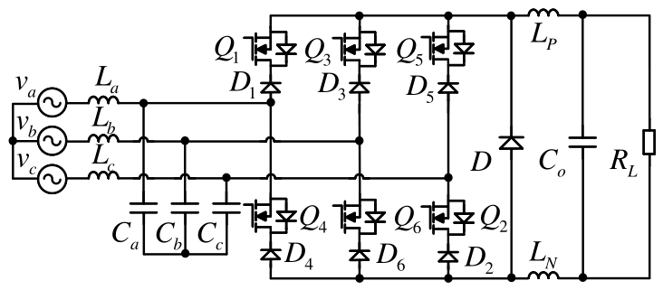
The three-phase rectifier serves as a crucial front-end power conversion stage in MEAs, efficiently converting generator AC power to a regulated DC bus voltage [
7,
8,
9]. Compared to the three-phase voltage source rectifier, the three-phase current source rectifier offers superior operational characteristics, including limited inrush current, wide output voltage regulation range, and inherent short-circuit protection, which establishes the three-phase current source rectifier as a preferred solution for MEA applications that demand high reliability and robust performance [
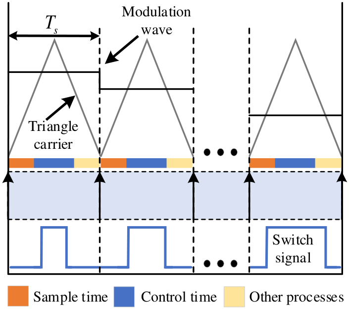
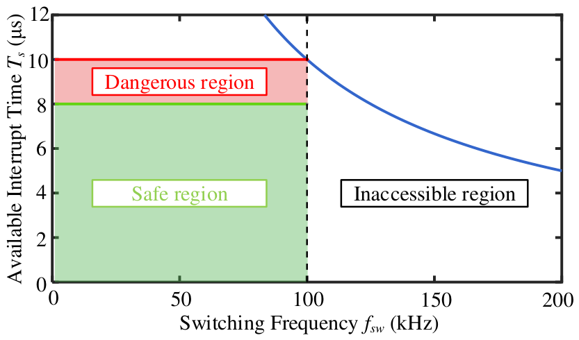
10]. Generally, a high switching frequency (100–200 kHz) is required for aviation three-phase current source rectifiers to enhance power density and reduce current harmonic distortion. Nevertheless, the short interrupt cycle, stemming from high switching frequency operation, poses significant challenges for cycle-by-cycle control of three-phase current source rectifiers, because analog-to-digital (ADC) conversion, digital signal filters for electromagnetic interference noise mitigation, overcurrent/overvoltage protection, and main control scheme execution should be implemented within such a short interrupt cycle [
11,
12,
13].
Beyond more electric aircraft, three-phase converters operating at switching frequencies of 50–100 kHz have considerable potential in high-performance AC–DC power-conversion applications. A higher switching frequency shifts the dominant switching harmonics toward a higher-frequency range, thereby facilitating the reduction of input and output filter size. When accompanied by a sufficiently high control-input update rate, it can also improve input-current tracking, reduce delay-induced current distortion, and enhance DC-link voltage regulation under dynamic load conditions. These characteristics are attractive for the grid-side AC–DC interfaces of photovoltaic and energy-storage systems, DC microgrids, and electric-vehicle fast-charging stations. The heterogeneous and time-varying charging-power profiles reported in [
14] further indicate the need for fast and reliable regulation in the AC–DC front-end stage of DC fast chargers. High-frequency conversion is also important in inductive power-transfer systems because it enables compact magnetic couplers and power-conversion stages. However, the associated switching losses, electromagnetic interference, and thermal-management requirements must be carefully considered, as demonstrated by the thermal analysis of a high-frequency inductive power-transfer system in [
15]. Therefore, the proposed multirate control principle may provide a useful grid-side control solution for these applications, although further application-specific investigations at higher power levels are required.
Regarding cycle-by-cycle control for three-phase current source rectifiers, extensive literature has been published in recent years due to their high control performance. A passivity-based nonsingular terminal sliding-mode control was proposed in [
16]. The control strategy combines the advantages of passivity-based control and nonsingular terminal sliding mode control, achieving resonance suppression, improving dynamic response, reducing chattering associated with traditional sliding mode control, and enhancing system robustness. In [
17], a simplified switch short-circuit fault-tolerant scheme for the three-phase current source rectifier was implemented. By paralleling two diodes in each phase without affecting the active switch, an effective fault-tolerant structure is constructed to withstand multiple switch short-circuit faults. A model predictive control strategy is proposed in [
18] for multi-objective control, which improves the robustness of the system and the performance of grid current reference tracking. A direct carrier-based modulation scheme was proposed in [
19] to reduce the ripple of DC-link current over the whole index range. Although these control schemes can achieve cycle-by-cycle control and improve the control performance of three-phase current source rectifiers in various aspects, their practical adoption is constrained by the high computational burden, which leads to interrupt execution overruns in the short interrupt cycle at high switching frequencies.
Apart from low-switching-frequency cycle-by-cycle control schemes, extensive research has investigated high-switching-frequency control schemes for three-phase current source rectifiers. A reconstructed phase voltages-based power following control under unbalanced input phase voltages was proposed in [
20]. By reconstructing the input phase voltage, this technique produces a modulation signal that is more balanced than the input phase voltage. The imbalance in the input current is reduced by regulating it to be proportional to the rebuilt phase voltage. However, the scheme creates three control interrupts to reduce the computational burden, the quickest of which is 100 kHz and cannot match the 200 kHz switching frequency. The authors of [
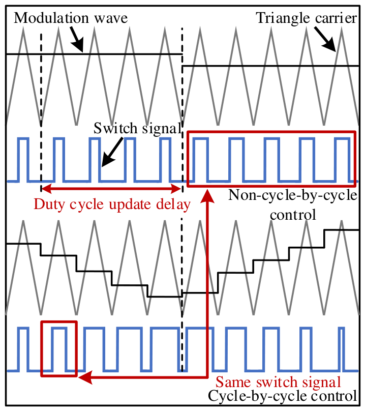
21] investigated the starting inrush current problem of the three-phase current source rectifier, analyzed in detail the mechanism of rectifier starting inrush current generation, and proposed a soft starting scheme and its starting curve design method based on this. However, the control frequency of this scheme is limited to only 50 kHz by the inadequate computing capacity of the microprocessor, leading to incompatibility with the 150 kHz switching frequency. It should be noted that these methods achieve high switching frequencies at the expense of non-cycle-by-cycle control, leading to control input multiplexing in the generation of switching signals and introducing inherent quantization errors and delays that degrade control performance.
In addition to basic power conversion and waveform regulation, modern digitally controlled converters increasingly incorporate online estimation, diagnostic, and resilient-control functions. Lu et al. proposed a differential impedance-detection method using a series–parallel direct-injection soft open point, which distinguishes feeder impedance from the overall grid impedance and further separates transformer and cable contributions through converter-based reactive-current injection without additional external detection equipment [
22]. Lin et al. developed a detection-free neural DC-link voltage-correction method based on a dual-stream denoising scheme for cyber-resilient solid-state transformers, demonstrating the role of signal reconstruction and data-driven correction in maintaining reliable converter operation under corrupted voltage information [
23]. Although these studies address different converter topologies and control objectives, they demonstrate that emerging power-electronic systems must execute increasingly complex estimation, signal-processing, and resilience-related tasks in addition to conventional feedback control and PWM generation. This trend further motivates digital architectures that provide sufficient computational time while retaining high-rate modulation-input updating.
Multirate control and predictive input generation have previously been investigated to alleviate the computational burden of high-switching-frequency power converters. Multirate finite-control-set model predictive control uses a lifted converter model to predict fast-rate state variables from slow-rate measurements and optimizes a sequence of switching states or voltage vectors within one sampling interval [
24,
25]. Predictive duty-cycle methods calculate or optimize duty-ratio corrections for specific objectives, such as neutral-point voltage-fluctuation and input-current-harmonic suppression [
26]. Digital-delay-compensation methods predict or advance a control command to compensate for calculation and PWM-update delays [
27,
28,
29].
The proposed method addresses a different implementation problem. It establishes a general rate-decoupled framework that separates computationally intensive control-input generation from switching-cycle-scale control-input application. Instead of holding one control input for N switching periods, the slow-rate task generates an online N-element sequence of distinct future control inputs, and the fast-rate task applies one sequence element during each switching period. Unlike multirate finite-control-set predictive control, the implementation presented in this paper does not require switching-state enumeration or online optimization of a converter-state trajectory. Unlike one-step delay compensation, it increases the number of distinct control inputs applied within one slow-rate interval rather than only advancing one command.
The framework is not inherently restricted to a particular converter topology or control algorithm. It can be combined with different converter topologies and control methods, provided that the slow-rate task can generate a sequence of future control inputs and that the fast-rate PWM task can apply them sequentially. In this paper, second-order Lagrange interpolation is used for sequential-input generation, and the framework is combined with indirect current control and SVPWM and experimentally verified on a three-phase current source rectifier.
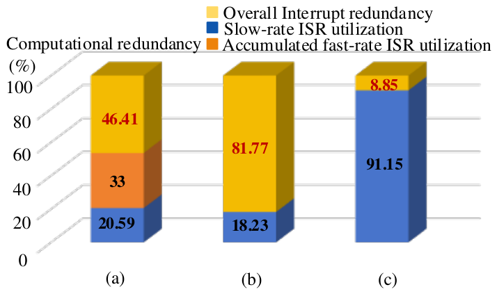
In the experimental implementation, kHz, , and kHz. Thus, , whereas . One slow-rate calculation generates ten distinct control inputs that are applied at 10 s intervals. The conventional 10-kHz and 50-kHz implementations hold one input for ten and two switching periods, respectively, and produce input-current THDs of 14.50% and 6.06%. The proposed framework applies one distinct input per switching period and reduces the THD to 4.02%. Considering both interrupt levels, the proposed implementation requires for the slow-rate ISR and for the ten fast-rate ISR executions within each slow-rate interval. The resulting overall processor utilization is 53.59%, leaving 46.41% overall computational redundancy, compared with only 8.85% for the conventional 50 kHz implementation.
In view of this, the main contributions of this paper are summarized as follows:
- (1)
A multirate quasi-cycle-by-cycle control framework is proposed to decouple the control calculation from the control-input update. The control calculations are performed in the slow-rate interrupt, while distinct control inputs are applied cycle by cycle in the fast-rate interrupt.
- (2)
A sequential control-input generation and transfer mechanism is developed. Lagrange interpolation is used to generate N sequential control inputs, which are reliably transferred between the slow-rate and fast-rate interrupts using dual data arrays and timestamp verification.
- (3)
The proposed scheme is experimentally validated on a three-phase current source rectifier operating at a switching frequency of 100 kHz. The input-current THD is reduced from 14.50% to 4.02%, while 46.41% overall computational redundancy is maintained after accounting for both the slow- and fast-rate ISR workloads.
In this paper, true cycle-by-cycle feedback control refers to an implementation in which the system states are sampled, the feedback controller is evaluated, and the control input is updated during every switching period. In contrast, the proposed quasi-cycle-by-cycle scheme samples the system states and evaluates the feedback controller at the slow rate, generates N sequential control inputs, and applies one prepared input during each of the subsequent N switching periods. Therefore, “cycle-by-cycle” describes the control-input application rate, whereas “quasi” indicates that no new state feedback is acquired during the fast-rate sequence execution.
The rest of this paper is organized as follows.
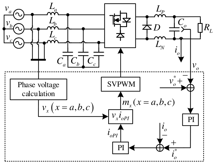
Section 2 presents the conventional indirect current control scheme and systematically analyzes the limitations of implementing cycle-by-cycle control for three-phase current source rectifiers at high switching frequency. In
Section 3, the proposed multirate quasi-cycle-by-cycle control scheme for the three-phase current source rectifier is introduced, and the configuration and digital implementation of fast-rate and slow-rate interrupts are also explained. The experimental results are then presented in
Section 4.
Section 5 discusses the applicability and limitations of the proposed method, and
Section 6 concludes the paper.
3. Proposed Multirate Quasi-Cycle-by-Cycle Control Scheme
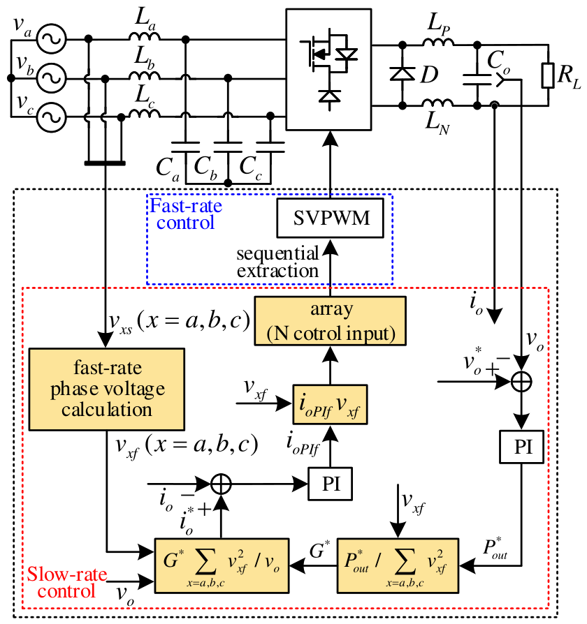
To address the conflict between short interrupts and the control overhead required for high-performance control under high-switching-frequency operation, a multirate quasi-cycle-by-cycle control scheme is proposed. In the proposed scheme, system-state sampling and computationally intensive feedback-control calculations are executed in the slow-rate interrupt, where a sequence of future control inputs is generated. The prepared sequence is subsequently extracted and applied in the fast-rate interrupt, with one sequence element applied during each switching period. No new system-state measurement or feedback-controller evaluation is performed during the fast-rate sequence execution. The overall control diagram is shown in
Figure 6. The proposed multirate quasi-cycle-by-cycle control scheme consists of three steps. First, the Lagrange interpolation calculation of a set of sequential control inputs during the slow-rate interrupt is proposed, which uses multiple control inputs to avoid interrupt execution overrun. Next, the process of extracting these sequential control inputs within the fast-rate interrupt is explained to ensure real-time updates of the control input. Finally, the digital implementation of the proposed multirate quasi-cycle-by-cycle control is presented, including detailed descriptions of both the fast-rate and slow-rate interrupt configurations. Additionally, a comprehensive theoretical analysis is conducted to examine the characteristics of truncation error.
3.1. Sequential Control Inputs Calculation in Slow-Rate Interrupt
To prevent interrupt execution overrun at high switching frequencies, most calculations in the proposed scheme are implemented in a slow-rate interrupt, ensuring sufficient interrupt time and avoiding interrupt execution overrun. Specifically, the proposed scheme first calculates
N control inputs during each slow-rate interrupt to prepare for the control input updates in subsequent fast-rate interrupts. The parameter
N determines the number of sequential modulation inputs applied within each slow-rate interval. It is selected according to the switching frequency and the slow-rate interrupt frequency as
where
represents the switching frequency, and
represents the slow-rate interrupt frequency. The fast-rate modulation-input application frequency is therefore
. It should be emphasized that
N increases the modulation-input application rate rather than the sampling frequency or the feedback-controller bandwidth. The output voltage/current sampling, PLL calculation, and voltage- and current-loop PI controllers are still executed at the slow-rate frequency
.
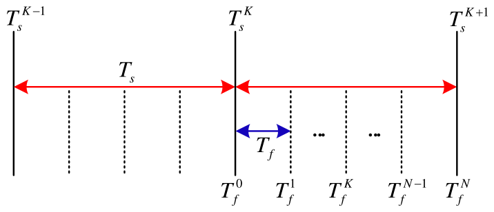
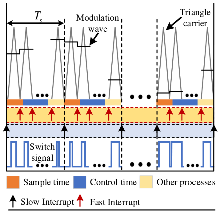
The proposed multirate framework is depicted in
Figure 7, where
and
denote the slow- and fast-rate interrupt periods, respectively. The three-phase voltages
are sampled at the slow-rate time points
,
, and
, with a sampling frequency of
. In the slow-rate interrupt period
to
, a set of sequential interpolated voltages
through Lagrange interpolation, using in the next slow-rate interrupt period at
,
, …,
. Therefore, the frequency relationship follows
(equivalently expressed as
) through uniform partitioning of the slow-rate period. Each slow-rate interrupt period initializes with the three-phase voltage values at
as the starting point.
where
represents the
Kth sampling point.
The phase angle values
,
,
corresponding to the phase voltages at each sampling point are calculated using a phase-locked loop. Subsequently, the corresponding angle for which the interpolation voltage point can be calculated as
where
represents the control point during the slow-rate interrupt from
to
.
These angle values are then processed using the standard second-order Lagrange polynomial interpolation formulation [
35,
36]. The corresponding Lagrange basis functions are expressed as
The sequential three-phase voltage inputs are subsequently reconstructed from the second-order Lagrange interpolation polynomial as [
35,
36]
Three adjacent voltage samples are employed because they constitute the minimum data set required for second-order Lagrange interpolation. This formulation captures the local curvature of the phase voltage while requiring fewer arithmetic operations and stored samples than higher-order interpolation. It also avoids the increased noise sensitivity and numerical oscillation that may accompany a higher interpolation order. Therefore, the three-point formulation represents a compromise among reconstruction accuracy, computational burden, memory usage, and real-time implementation capability. Its adequacy assumes that the phase voltage and the PLL-estimated phase angle vary smoothly within the local interpolation interval.
The interpolation does not require the input frequency to remain exactly constant. The interpolation nodes
,
, and
are obtained from the PLL, and the fast-rate angles in (
7) are calculated using the local angular increment
. Consequently, gradual frequency variations are reflected in the node spacing. In addition, the three phase voltages are interpolated independently; hence, unequal phase amplitudes under unbalanced conditions do not invalidate the interpolation. However, rapid frequency transients, large PLL errors, or severe voltage distortion can increase the reconstruction error. In particular, voltage distortion increases the local third-derivative bound
in the Lagrange remainder. Under such conditions, a higher slow-rate sampling frequency, adaptive interpolation, or improved phase estimation may be required.
The influence of sampled-voltage error can be evaluated by representing each measured sample as
. The corresponding error in the interpolated voltage is
If
, the error satisfies
For approximately uniformly spaced angular nodes and , . Therefore, bounded measurement noise is amplified by no more than approximately 25% under this condition. ADC quantization can be incorporated by replacing with , where is the ADC voltage resolution.
For a small PLL phase error
, the resulting voltage error can be approximated and bounded as
When the phase error is primarily caused by a PLL delay , , and hence . This relationship indicates that the effect of the PLL delay increases with the input angular frequency, the PLL delay, and the local voltage slope.
When the converter losses are neglected, the instantaneous input and output powers can be related using the power-balance and conductance-based current-shaping principle adopted for three-phase current-source rectifiers [
20,
34]. Therefore
where
G is the conductance of each phase on the input side.
From (
15), the given conductance can be expressed as
Therefore, the reference of the DC-side output current can be formulated as
For a converter with an efficiency of
, the loss-compensated equivalent input conductance is
Therefore, the nominal lossless model underestimates the required input conductance by relative to the loss-compensated value, while the required correction relative to the nominal conductance is . For example, assumed efficiencies of 90%, 94%, and 98% correspond to conductance underestimations of 10%, 6%, and 2%, respectively. Over the investigated output-power range of 136.5–409.5 W, the corresponding loss ranges are 15.17–45.50 W, 8.71–26.14 W, and 2.79–8.36 W. These efficiency values are used only as sensitivity parameters and are not measured efficiencies of the experimental prototype.
Substituting Equation (
16) into Equation (
17) gives
. Thus, when the same reconstructed phase-voltage values are used consistently in the two equations, the voltage-squared term cancels algebraically. Converter losses primarily increase the required input conductance and input-current amplitude. Moreover, the outer DC-voltage PI controller contains integral action and therefore compensates a constant loss-related power mismatch in steady state, provided that the controller remains stable and unsaturated. The lossless assumption consequently introduces a feedforward conductance bias and additional feedback correction rather than an uncompensated steady-state DC-voltage error.
Moreover, the output of the current loop is
at different
. The control inputs, which are used to generate gating signals via SVPWM to control the switches of the three-phase current source rectifier, are expressed as
In this way, a set of control inputs , ,…,,…, can be obtained in each slow-rate interrupt and placed in a specific array, waiting for the sequential extraction of subsequent fast-rate interrupts.
3.2. Sequential Control Inputs Extraction Cycle-by-Cycle in Fast-Rate Interrupt
To provide switching-cycle-scale control-input updating, one element of the
N-element sequence generated by the slow-rate task is extracted and applied whenever a fast-rate interrupt occurs. The sequence is executed without acquiring new system-state measurements during the current slow-rate interval. Therefore, the fast-rate task provides cycle-by-cycle input application rather than cycle-by-cycle feedback recalculation. As shown in
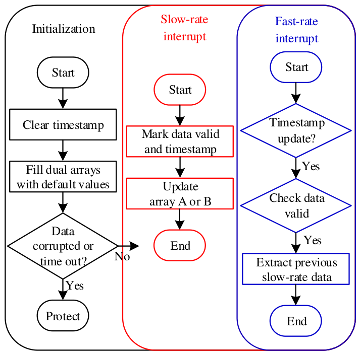
Figure 8, to ensure reliable extraction of control inputs from slow-rate interrupts during fast-rate interrupts and facilitate their real-time update, the proposed scheme employs a dual-array architecture with timestamp verification for data synchronization. This architecture effectively bridges the timing gap between different interrupt frequencies. More specifically, one array is designated as the active buffer and is read only by the fast-rate interrupt, whereas the other is designated as the inactive buffer and is written only by the slow-rate interrupt. After all
modulation inputs have been generated, the slow-rate routine updates the timestamp and validity flag and changes the active-buffer index within a short protected operation. At the beginning of each fast-rate interrupt, the active-buffer index is read once and retained throughout the current ISR execution. Therefore, the fast-rate interrupt always extracts data from one completely updated buffer and cannot access the buffer being written by the slow-rate interrupt.
Additionally, the scheme incorporates error-prevention and fault-tolerance mechanisms to enhance system reliability. Upon initialization, the dual-array architecture is populated with default values, and the timestamp is reset to prevent the accidental use of uninitialized data. In the event of data corruption or timing violations (e.g., exceeding two slow-rate interrupt cycles), the scheme automatically reverts to the last valid dataset, increments an error counter, and issues a system alarm. This ensures continuous operation even in the presence of transient faults, thereby improving robustness in real-time control applications. For 32-bit floating-point data, the memory required by the two three-phase modulation-input buffers is bytes. Therefore, the buffer-data memory is 240 bytes for , excluding the small additional memory required by the indices, validity flags, timestamps, and error counter.
3.3. Fast-Rate/Slow-Rate Interrupt Configuration and Digital Realization
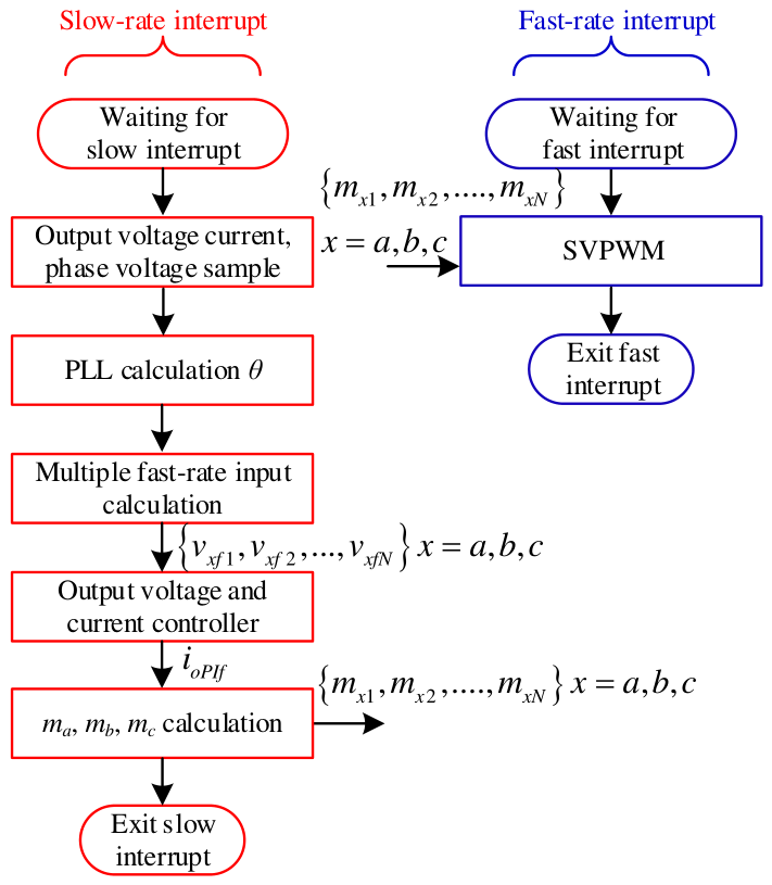
To achieve enhanced control frequency and cycle-by-cycle control performance, the digital implementation of the proposed scheme employs a multirate framework that decouples control into fast- and slow-rate parts, implemented in nested interrupts. The interrupt execution flowchart of the proposed scheme implemented in digital is shown in
Figure 9. The slow-rate interrupt handles all computationally intensive tasks, including output voltage/current sampling, input phase-voltage sampling, phase-angle derivation, sequential control-input calculations, and output regulation. The fast-rate interrupt is singularly dedicated to generating switch signals through SVPWM. Moreover, the digital implementation ensures that fast-rate interrupt modulation calculations are fully completed before the slow-rate interrupt is activated, with enforced isolation via minimum timing margins.
The controller is implemented on a TMS320F28377S DSP(Texas Instruments, Dallas, TX, USA) operating at a system clock frequency of 200 MHz. ADC sampling is initiated at the beginning of each slow-rate interval . The fast-rate interrupt is synchronized with the PWM carrier and is assigned a higher priority than the slow-rate interrupt. At each fast-rate instant , the extracted modulation inputs are written to the PWM shadow registers and transferred to the active registers at the immediately following predefined PWM carrier boundary. Therefore, the duty ratios are updated only at switching-period boundaries.
As shown in
Figure 10, in contrast to conventional single-rate implementations, the multirate framework necessitates elevating the carrier frequency to match the control frequency
to accommodate multiple modulation signals generated within each slow-rate interrupt. During the slow-rate interrupt, high-priority fast-rate interrupts can preempt operations to generate multiple switching signals. Upon completion of the fast-rate interrupt service routine, execution automatically returns to the preemption point in the slow-rate interrupt handler.
The measured slow-rate ISR execution time reported in this paper represents the active processor time consumed by the slow-rate task and excludes the intervals during which its execution is suspended by the higher-priority fast-rate ISR. Therefore, the slow-rate execution time cannot be used alone to represent the overall processor utilization. The complete processor workload must include both the slow-rate ISR and all fast-rate ISR executions occurring within the same slow-rate interval.
Consequently, a distinct modulation input and the corresponding switching signals are applied during every fast-rate period. This increases the modulation-input application rate from to without changing the slow-rate sampling, PLL, or PI-controller execution frequency.
In the experimental implementation, kHz, , and kHz. Therefore, new voltage and current measurements are acquired and the PLL and PI controllers are evaluated once every 100 s, whereas a distinct predicted modulation input is applied once every 10 s. The fast-rate interrupt does not acquire new feedback information or reevaluate the PI controllers. Consequently, the proposed method reduces the modulation-input holding error within each slow-rate interval but does not increase the closed-loop feedback bandwidth by a factor of N.
3.4. Truncation Error Analysis
The second-order Lagrange interpolation polynomial provides an approximation of the actual phase-voltage function at the fast-rate instants. Let
denote the actual voltage of phase
x, expressed as a function of the phase angle
, and let
denote its interpolated value at the
ith fast-rate instant within the
Kth slow-rate interval. The corresponding interpolation error is defined as
According to the classical remainder theorem for second-order Lagrange polynomial interpolation [
35,
36], there exists an intermediate point
within the smallest interval containing the three interpolation nodes and the evaluation point such that the interpolation remainder is determined by the third derivative of the phase-voltage function. Define
, where
denotes the interpolation interval. The interpolation-error bound can then be expressed as
In Equation (
21),
has the unit
, while the product of the three phase-angle differences has the unit
. Therefore, the resulting interpolation-error bound has the unit V, which confirms the dimensional consistency of the expression. The bound becomes zero at the interpolation nodes and is nonzero only at the intermediate fast-rate points.
It should be emphasized that Equations (
20) and (
21) describe the truncation error associated with approximating the actual phase-voltage function using a second-order interpolation polynomial. Round-off, coefficient quantization, ADC quantization, and other finite-word-length effects constitute additional numerical implementation errors and are not included in the classical interpolation remainder. These numerical effects should therefore be distinguished from the interpolation truncation error [
37].
The derived bound quantifies the phase-voltage interpolation error, whereas the resulting duty-ratio error depends on its propagation through the subsequent control and modulation calculations. To evaluate its propagation through Equations (
16)–(
19), define the phase-voltage interpolation error as
, with
. Furthermore, define
and
. The perturbation of the squared-voltage sum satisfies
For the balanced 115 V RMS input used in the experiment,
. Using the maximum measured interpolation error
gives
. If
and
, the corresponding conductance error satisfies
The DC-current reference does not have the same sensitivity because the same reconstructed squared-voltage sum is used in Equations (
16) and (
17). Consequently,
and the interpolation error does not directly introduce a steady-state bias into
. For the modulation input, a local sensitivity analysis with a fixed current-controller output gives
Since the phase-voltage peak is , the measured 0.2 V error corresponds to 0.123% of the phase-voltage peak. The conservative normalized error of the complete three-phase modulation vector is no greater than 0.174%. Within a fixed SVPWM sector, the duty ratios are piecewise-linear functions of the modulation vector; therefore, the resulting duty-ratio perturbation is of the same small order. However, its exact instantaneous value also depends on the active sector, modulation index, and current-controller output, and a universal duty-ratio bound cannot be obtained from the voltage error alone.
4. Experimental Verification
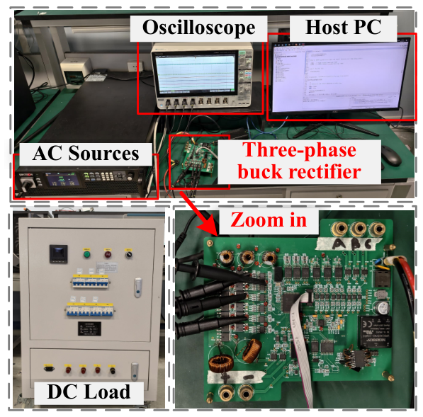
To verify the effectiveness of the proposed multirate quasi-cycle-by-cycle control scheme, an experimental prototype of a 400 W three-phase current source rectifier has been designed and built as shown in
Figure 11, whose detailed parameters are listed in
Table 2.
The parameters were selected to construct a representative scaled laboratory prototype for more-electric-aircraft power-conversion applications. The 115-V/400-Hz AC input represents a typical aircraft AC supply, whereas the 200-V DC output and approximately 400-W power level were selected according to the ratings of the laboratory source, semiconductor devices, DC load, and measurement equipment. The switching frequency was set to 100 kHz to evaluate the proposed method under a short switching period of 10 s. Accordingly, the slow-rate and fast-rate interrupt frequencies were set to 10 kHz and 100 kHz, respectively, resulting in a sequence length of . The input- and DC-side filter parameters were selected to attenuate the switching ripple and ensure stable operation under the investigated condition.
These parameters are representative experimental values rather than mandatory values of the proposed method. The multirate framework is not inherently restricted to the investigated voltage, power, or input-frequency levels. However, the fast-rate interrupt must be completed within each switching period, while the slow-rate calculation and sequence preparation must be completed before the next data transfer. Moreover, the slow-rate frequency and sequence length must provide sufficient interpolation accuracy. Therefore, extending the proposed method to higher power levels or more severe operating conditions requires appropriate redesign of the power stage, passive components, protection circuits, and control parameters.
In the prototype, metal–oxide–semiconductor field-effect transistors (MOSFETs) STD18N65M5 (STMicroelectronics, Plan-les-Ouates, Switzerland) are used. The DSP TMS320F28377S is used to implement the proposed scheme.
Two non-cycle-by-cycle control schemes are designed for comparison: one with an interrupt frequency set at 10 kHz (equal to the slow-rate interrupt frequency in the proposed scheme) and the other at 50 kHz (the fastest frequency without interrupt execution overrun). In the proposed scheme, the slow-rate interrupt frequency is set to 10 kHz, and the fast-rate interrupt frequency is set to 100 kHz. The same proportional and integral gains are intentionally used for the voltage and current controllers in all three experimental cases, and the PI gains are not independently retuned for each implementation. In the proposed scheme, both PI controllers are evaluated in the 10 kHz slow-rate interrupt, which is identical to the PI-controller execution rate of the 10 kHz non-cycle-by-cycle baseline. Only the sequential modulation-input application rate is increased to 100 kHz through the fast-rate interrupt. Therefore, the comparison between these two cases keeps the PI gains, PI execution rate, switching frequency, power stage, and operating conditions unchanged, thereby isolating the influence of the control-input updating mechanism.
The 50 kHz non-cycle-by-cycle scheme represents the highest conventional control frequency that can be executed on the adopted DSP without interrupt execution overrun. It is included as a supplementary reference for evaluating the effects of a shorter control-input holding interval and a reduced computational margin. The reported results therefore constitute a matched-controller comparison and are not intended to claim superiority over every independently retuned conventional controller.
4.1. Steady-State Performance
To validate the steady-state performance of the proposed scheme, experimental tests were first conducted to verify the stable operation of the three-phase current source rectifier. The comparative analysis is conducted at the same switching frequency (
kHz) to achieve a fair comparison. In the test, the three-phase current source rectifier operates at an output power (
W) with an AC input frequency (
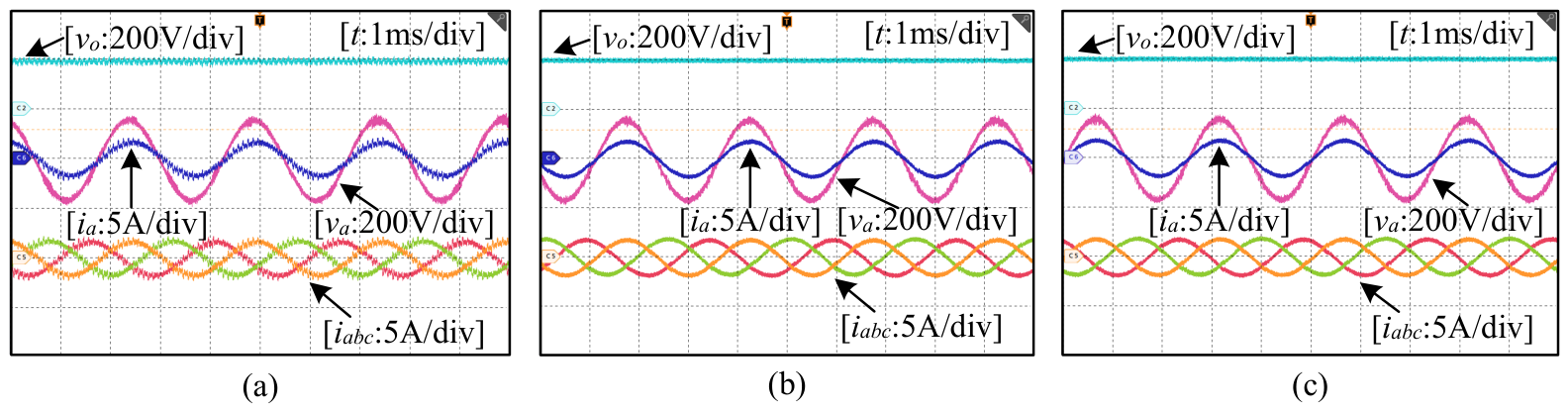
Hz). The steady-state performance of the three-phase current-source rectifier under three control schemes is shown in
Figure 12. From top to bottom, the waveform is DC-link output voltage
, phase-
a grid voltage
, phase-
a grid current
, and three-phase grid currents
. As shown in
Figure 12, all three control schemes exhibit high sine values for the three-phase input current and a stable 200 V output voltage, while maintaining unity power factor. However, the proposed scheme provides improved input-current quality and lower output-voltage ripple because it replaces one control input held for multiple switching periods with a sequence of distinct control inputs applied at the switching frequency. This result demonstrates the benefit of switching-cycle-scale control-input updating rather than equivalence to true cycle-by-cycle feedback control.
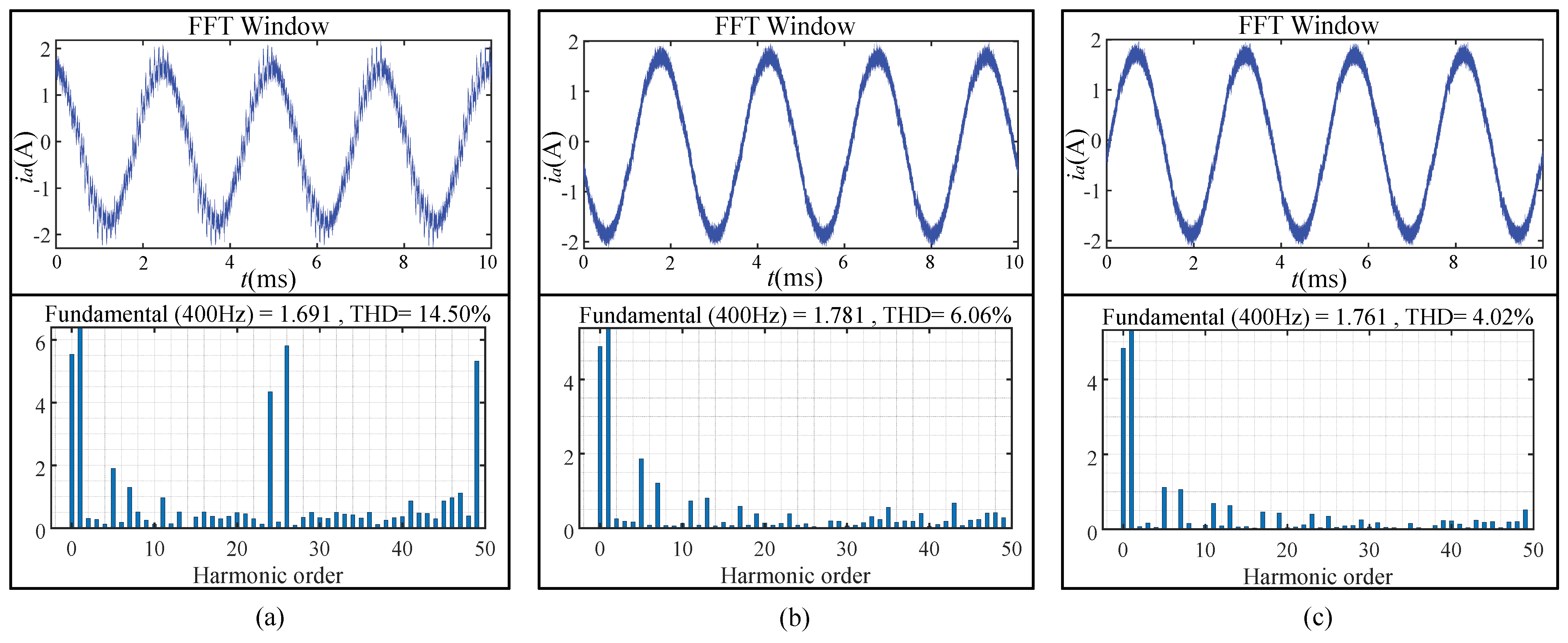
Furthermore, the fast Fourier transform (FFT) spectrum analysis of the phase-
a current is shown in
Figure 13. The current waveform analysis reveals that non-cycle-by-cycle control (
kHz) exhibits poor performance with significant current ripple and high total harmonic distortion (THD) of 14.5%. As the control frequency increases to (
kHz), THD drops to 6.06%. In contrast, the proposed scheme (
kHz,
) achieves THD of 4.02%, representing a 72.27% improvement compared to the non-cycle-by-cycle control scheme benchmark (
kHz).
4.2. Dynamic-State Performance
In addition to the steady-state performance verification discussed earlier, the dynamic-state performance of the proposed scheme is tested to verify its closed-loop regulation capabilities under DC-link voltage reference variations and DC-link load switching.
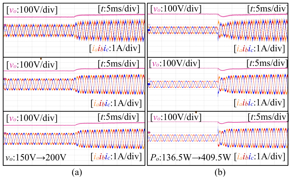
(1) DC-link voltage reference variation: The DC-link load is assumed to be a constant value, and the process of changing the DC-link voltage reference from 150 V to 200 V is shown in
Figure 14a. From top to bottom, the waveform is the DC-link output voltage
, three-phase grid currents
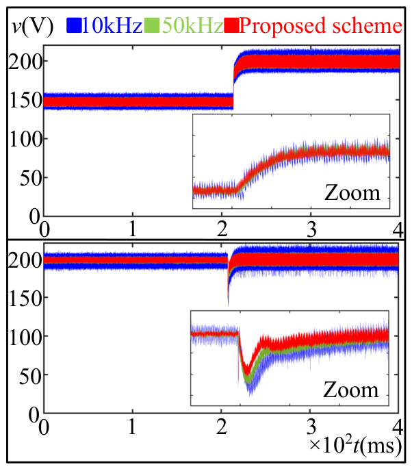
. The proposed scheme reduces the current ripple without affecting the dynamic performance of non-cycle-by-cycle control schemes. As shown in the upper part of
Figure 15, the proposed scheme produces a smoother transient waveform and lower output-voltage ripple by reducing the modulation-input holding error. However, the response to newly sampled feedback information is still determined by the 10 kHz slow-rate control loop.
(2) DC-link Load Switching: Furthermore, the DC-link voltage reference is assumed to be a constant value, and the dynamic test with load switching from 136.5 W to 409.5 W is shown in
Figure 14b and the bottom of
Figure 15. It can be observed that all schemes exhibit a rapid response to the external disturbance. Compared with the non-cycle-by-cycle control schemes, the proposed scheme produces fewer spikes in the three-phase input currents and a smoother output-voltage waveform during the tested load transient. These improvements result from the switching-cycle-scale updating of the modulation input rather than an
N-fold increase in the feedback-controller bandwidth.
As summarized in
Table 3, the proposed scheme achieves a reference-step settling time of 18.85 ms, comparable to 19.13 ms and 18.97 ms for the conventional 10 kHz and 50 kHz schemes, respectively, while reducing the voltage undershoot, output-voltage ripple, and peak input current to 4.7 V, 9.4 V, and 1.87 A. Under the load step, the recovery time decreases to 14.56 ms, corresponding to reductions of 10.57% and 16.03% relative to the two conventional schemes. The voltage undershoot decreases from 62.3 V and 48.7 V to 39.8 V, while the output-voltage ripple and peak input current decrease to 10.1 V and 1.92 A. These results demonstrate comparable reference-tracking speed, improved voltage and current characteristics, and faster recovery from the investigated load disturbance.
In conclusion, the proposed scheme reduces the current spikes, output-voltage ripple, and control-input holding delay under the tested transient conditions by applying a distinct modulation input during every switching cycle. Nevertheless, the sampling, PLL, and PI-controller execution frequencies remain at 10 kHz. Therefore, the response to newly sampled disturbances and reference changes is still limited by the slow-rate feedback loop, and the proposed scheme should not be interpreted as increasing the closed-loop bandwidth by a factor of N.
4.3. Truncation Error Analysis
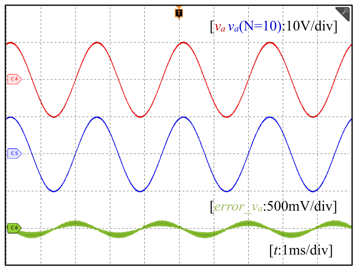
To validate the accuracy of the reconstructed phase voltage by Lagrange interpolation under the proposed scheme, the truncation error of the Lagrange-interpolated phase-
a voltage is shown in
Figure 16. From top to bottom, the waveform is the measured and filtered phase-
a voltage, the reconstructed phase-
a voltage by Lagrange interpolation, and the truncation error of the Lagrange-interpolated phase-
a voltage. As shown in
Figure 16, the maximum observed interpolation error of the phase-
a voltage is approximately 0.2 V. Relative to the 162.63 V phase-voltage peak, this error is 0.123%. According to the propagation analysis in
Section 3.4, conservatively applying the same error bound to all three phases results in a maximum squared-voltage-sum error of 0.348%, an equivalent-conductance error of less than 0.349%, and a normalized three-phase modulation-vector error of less than 0.174%. The DC-current reference
is not directly biased because the reconstructed squared-voltage sum cancels between Equations (
16) and (
17). These results indicate that the interpolation process introduces only a small additional perturbation into the sequential modulation inputs. The measured current THD cannot be derived directly from the voltage interpolation error because it also depends on the input filter, PWM mapping, controller dynamics, and converter nonidealities. Therefore, the THD improvement reported in
Table 4 is attributed primarily to updating the modulation input in every switching cycle, while the small interpolation error confirms that the high-rate input sequence does not introduce a significant additional modulation disturbance.
4.4. Computational Redundancy Comparison
To evaluate the complete computational burden of the proposed multirate implementation, the execution times of both the slow-rate and fast-rate ISRs must be considered. The overall processor utilization within one slow-rate interval is defined as
where
and
denote the active processor execution times of one slow-rate ISR and one fast-rate ISR, respectively. The overall computational redundancy is then defined as
For the proposed scheme,
,
,
, and
. Because ten fast-rate ISR executions occur within each slow-rate interval, the total processor time required by the two interrupt levels is
Accordingly, the overall processor utilization is 53.59%, and the overall computational redundancy is 46.41%. The previously reported value of 79.41% represents only the slow-rate-task timing margin when the fast-rate ISR workload is not included; therefore, it is not used as the overall computational redundancy of the complete multirate implementation. As illustrated in
Figure 17, the processor utilization of the proposed scheme consists of 20.59% slow-rate ISR utilization and 33.00% accumulated fast-rate ISR utilization, leaving 46.41% overall computational redundancy.
For the conventional scheme operating at 10 kHz, the measured ISR execution time is
within a
interrupt period, resulting in a processor utilization of 18.23% and a computational redundancy of 81.77%. When the conventional interrupt frequency is increased to 50 kHz, the same ISR is executed once every
. Consequently, its processor utilization increases to 91.15%, leaving only 8.85% computational redundancy. The overall processor utilization, computational redundancy, and input-current THD of the three schemes are summarized in
Table 4.
All three control schemes in
Table 4 were experimentally evaluated using the same converter prototype, switching frequency of 100 kHz, input and output operating conditions, and voltage- and current-loop PI parameters. For the 10-kHz non-cycle-by-cycle scheme, the measured ISR execution time is 18.23
s within a 100
s interrupt period, leaving 81.77
s of available computational time. However, because the same control input is held for ten consecutive switching cycles, the input-current THD reaches 14.50%. Increasing the conventional control frequency to 50 kHz reduces the THD to 6.06%, but the interrupt period decreases to only 20
s. Since the ISR execution time remains 18.23
s, only 1.77
s of available computational time remains, corresponding to a computational redundancy of 8.85%.
For the proposed scheme, the computationally intensive operations are performed in the 10-kHz slow-rate interrupt, while ten distinct control inputs are sequentially applied at the 100-kHz switching frequency. The measured slow-rate ISR execution time is 20.59 s within a 100 s slow-rate period, leaving 79.41 s of available computational time. Compared with the 10-kHz non-cycle-by-cycle scheme, the proposed scheme increases the slow-rate ISR execution time by only 2.36 s, while reducing the input-current THD from 14.50% to 4.02%, corresponding to a relative reduction of 72.28%. Compared with the 50-kHz non-cycle-by-cycle scheme, the proposed scheme further reduces the THD from 6.06% to 4.02%, while maintaining substantially greater computational redundancy. These results demonstrate that the proposed scheme improves the control-input update resolution and input-current quality without requiring the complete control algorithm to be executed within every switching period.
It should be noted that the reduction in THD from 14.50% to 4.02% in the primary comparison is not caused by different PI gains or a higher PI-controller execution rate. Both the proposed scheme and the 10 kHz non-cycle-by-cycle scheme use the same PI gains and evaluate the PI controllers at 10 kHz. The difference is that the conventional scheme holds one modulation input for ten switching cycles, whereas the proposed scheme generates ten sequential modulation inputs in each slow-rate interval and applies a distinct input during every 100 kHz switching cycle. The 50 kHz baseline reduces the holding interval to two switching cycles and consequently decreases the THD to 6.06%, but it is limited by the available interrupt execution time. These results indicate that the main improvement arises from the switching-cycle-scale updating of the modulation input rather than from PI-gain retuning.
5. Discussion
The experimental results demonstrate that the improved input-current quality is mainly attributed to the increased control-input update resolution. In the conventional 10-kHz non-cycle-by-cycle scheme, the same control input is held for ten consecutive switching cycles, resulting in a control-input holding effect and an input-current THD of 14.50%. Increasing the conventional control frequency to 50 kHz reduces the THD to 6.06%, but decreases the computational redundancy to only 8.85%. In contrast, the proposed scheme generates ten distinct control inputs during each 10-kHz slow-rate interval and sequentially applies them at the 100-kHz switching frequency. Consequently, the input-current THD is reduced to 4.02%, while an overall computational redundancy of 46.41% is retained after accounting for both the slow- and fast-rate ISR workloads. Compared with the conventional 10-kHz scheme, the proposed method increases the ISR execution time by only 2.36 s but reduces the THD by 72.28%, demonstrating a favorable balance between control performance and computational feasibility.
The proposed multirate implementation provides a potential solution for high-switching-frequency AC/DC converters in which the complete control algorithm cannot be executed within every switching period. However, the sequence length and slow-rate frequency must be selected by considering the switching frequency, computational burden, timing safety margin, and interpolation accuracy. A larger sequence length provides more computation time but may increase the interpolation error under distorted or rapidly varying input-voltage conditions. Moreover, the present experimental validation is limited to a 409.5 W prototype operating with a 115 V/400 Hz input, a 200 V DC output, and a switching frequency of 100 kHz. Extension to higher-power converters or other applications, including electric-vehicle charging and inductive power-transfer systems, requires application-specific hardware design, control-parameter adjustment, and further experimental validation. Future work will investigate higher-power operation, nonideal input conditions, efficiency, thermal performance, and electromagnetic interference.
The proposed multirate-decoupled framework is not inherently restricted to the approximately 400 W prototype. Extension to higher power requires appropriate semiconductor ratings, passive components, sensing ranges, controller parameters, and cooling arrangements. Higher switching frequencies also require renewed timing analysis: operation at with would require and a fast-rate period of s. Both the fast-rate execution deadline and the increased sequence-generation workload must be accommodated. Increasing N raises the control-input update rate but does not proportionally increase the feedback bandwidth. Furthermore, switching and conduction losses, junction temperature, commutation overshoot, and current stress must be evaluated, together with EMI filtering, layout, and gate-drive requirements. Improved input-current THD does not by itself demonstrate conducted or radiated EMI compliance. Protection based solely on the 10 kHz slow-rate sampling task may incur a detection delay approaching s before processing and actuation delays are included. A dedicated fast protection path should therefore override the buffered control inputs independently of the slow-rate calculation while preserving a safe path for the DC-link inductor current. Accordingly, the present experiments validate the proposed scheme at approximately 400 W and 100 kHz, whereas higher-power operation, 200 kHz switching, and aviation qualification require further dedicated validation.