
Article

A Back-Gate Corner-Closure Methodology for All-Digital Multi-Modulus Dividers in 22 nm FDSOI

Department of Electrical and Computer Engineering, Iowa State University, Ames, IA 50011, USA
*
Author to whom correspondence should be addressed.
Electronics 2026, 15(17), 4036; https://doi.org/10.3390/electronics15174036
Submission received: 10 July 2026 / Revised: 17 August 2026 / Accepted: 2 September 2026 / Published: 7 September 2026
(This article belongs to the Special Issue Feature Papers in Circuit and Signal Processing, 2nd Edition)

Abstract

The first divider in the feedback path of a frequency synthesizer runs at the full oscillator frequency and so constrains the speed and the power of the loop. Current-mode logic reaches high speed but draws a constant bias current independent of switching activity, whereas an all-digital, fully static-CMOS divider draws only dynamic and leakage current at the cost of far greater timing sensitivity to process, voltage, and temperature (PVT) variation. This paper presents a wide-range all-digital multi-modulus divider in 22 nm fully depleted silicon-on-insulator (FDSOI) technology, together with the methodology that makes the digital approach robust. The chain exhibits three distinct PVT failure modes, setup at the slow corners, hold at the fast-cold corner, and collapse of the internal clock duty cycle at the skewed corners; each is identified analytically and closed by a scheme combining back-gate body bias, a per-stage programmable delay trim, and a systematic integral-nonlinearity trim. Characterization is by post-layout simulation over a 45-point corner matrix, with the applied back-gate rail voltages and trim codes reported for every point. The divider covers N = 8 to 127, reaches 39.5 GHz at the typical corner, and holds a worst-case 33.0 GHz across the corner box against a 33 GHz target that the uncompensated chain misses at the slow and skewed low-supply corners (SS, SF, and FS at 0.72 V). A paired Monte Carlo campaign of 100 samples with process and mismatch variation, run at the binding corner, raises the yield at the target from 39% uncompensated to 72% with a single global back-gate setting and 99% with a per-die setting. At the target the divider consumes 5.3 mW at N = 127 ( 6.2 GHz/mW) with 35.2 fs of additive jitter in a 0.005   mm 2 core. The bias and trim settings are chosen by an external search and applied as fixed per-corner values; the monitors, controller, and bias generator that an autonomous implementation would require are specified but not designed, so the work demonstrates externally calibrated corner closure rather than a self-contained compensation system.

1. Introduction

The programmable frequency divider in the feedback path of a phase-locked loop (PLL) is one of the few blocks that must operate at the full output frequency of the voltage-controlled oscillator, and it therefore sets a practical limit on both the speed and the power budget of an integer- or fractional-N frequency synthesizer [1,2]. In the millimeter-wave synthesizers of 5G FR2 transceivers, automotive radar, and point-to-point links, this divider must run at input frequencies of several tens of gigahertz while covering a wide, contiguous division range that serves multiple bands and channel rasters from a single reference. The 33 GHz, N = 8 to 127 design point of this work corresponds to reference frequencies of roughly 0.26 to 4.1 GHz. The multi-modulus divider (MMD), formed by cascading modular divide-by-2/3 cells, has become the standard architecture for this function because it provides a wide, contiguous division range with a regular and power-scalable structure [1].
A long-standing tension governs the implementation of these cells. Current-mode-logic (CML) realizations achieve high speed and low jitter, but each latch holds a constant differential bias current whenever the circuit is powered, so the static power is fixed by the bias and does not fall with activity [3,4,5]. A fully static-CMOS implementation removes this bias entirely and draws only dynamic switching current together with leakage, so its power scales with activity and drops sharply in the later stages that run at divided frequencies [6,7,8]. The price of the static-CMOS choice is that the timing of digital logic is far more sensitive to process, voltage, and temperature (PVT) variation than that of a current-biased latch, which is precisely why designers often default to CML at the front of the chain.
This work takes the opposite position and keeps the entire divider all-digital, then treats the resulting PVT sensitivity as a problem to be solved by design rather than avoided by topology. The chosen technology, a 22 nm fully depleted silicon-on-insulator (FDSOI) process, is particularly well matched to this goal because its buried-oxide back gate provides a continuous threshold-voltage knob with a large tuning range, which has been used to compensate full process and temperature spread in digital and mixed-signal blocks [9,10,11]. The back gate has already been applied to dividers in this technology: a divide-by-four E-TSPC prescaler in 22 nm FD-SOI uses the n-well and p-well voltages to shift its self-resonance frequency and so reduce the input amplitude required for correct division, reaching 70 GHz in measurement [12,13]. That work tunes an operating point of a fixed-ratio prescaler; it does not identify the corner-dependent failure modes of a wide-range programmable chain, nor close them with a per-corner bias plan. Multi-modulus TSPC dividers have likewise been verified across corners: a 17 GHz seven-ratio divider in 65 nm CMOS is signed off over process, supply, and temperature with extracted parasitics [14]. That verification, however, establishes that a fixed design passes by margin, not that a failing corner can be recovered by a knob. Despite the maturity of both the MMD architecture and FDSOI body biasing, to the authors’ knowledge no published work combines them into a reproducible methodology that predicts each corner failure of an all-digital divider and closes it with a defined knob, and none reports which corner fails, by how much, and what it costs to close it. This gap has practical consequences: an uncompensated all-digital chain of the kind proposed here in fact fails to meet the target frequency at the slow-hot corner. Closing that corner, so that the speed holds across the full process and temperature box, is the problem this work addresses.
The contributions of this paper are therefore as follows. First, a wide-range all-digital MMD is described that removes the static bias current of CML and balances speed against power across its stages using digital cells only. Second, the three PVT failure modes of the all-digital chain are identified and analyzed. Third, a three-method compensation scheme is presented and shown to close each failure mode. Body biasing is itself an established 22FDX technique; the contribution here is its systematic application to a 33 GHz all-digital divider, in particular the independent n-well and p-well biasing that rebalances the internal duty cycle at the skewed corners. The scheme combines this global knob with a per-stage delay trim, a bounded integral-nonlinearity trim, and the corner-closure flow that ties the three together. Fourth, a complete post-layout corner and Monte Carlo verification flow is defined, and the power is compared against the measured power of published CML dividers, with an analytical bound on the CML bias current used to characterize the mechanism, namely the always-on, frequency-proportional bias that the all-digital chain avoids, rather than to assert a power magnitude. The scope of these contributions should be read precisely. Throughout this work the back-gate and trim settings are selected by an external search and applied as fixed per-corner or per-die values. The monitors, adaptive controller, bias generator, calibration logic, and code storage that an autonomous implementation would require are specified in Section 2.5, but they are neither designed nor validated here. What is demonstrated is therefore a reproducible, externally calibrated corner-closure methodology, not a self-contained adaptive compensation system. The remainder of the paper presents the architecture and methods (Section 2), the simulation results (Section 3), a discussion (Section 4), and conclusions (Section 5).

2. Materials and Methods

2.1. Divider Architecture and Governing Equation

The proposed MMD is built as a cascade of programmable divider cells in the modular style introduced by Vaucher [1], in which each cell divides by 2 or 3 under the control of a single modulus bit and passes a modulus-request signal backward along the chain. A chain of n such cells produces a programmable division ratio
N = 2 n + i = 0 n 1 p i 2 i ,
where p i { 0 , 1 } is the program bit of stage i. The base chain covers the contiguous interval N [ 2 n , 2 n + 1 1 ] , and the six-stage realization considered here reaches a maximum ratio of N = 127 when all stages are active. To extend the range below 2 n without a discontinuity, the later cells support a transparent divide-by-1 mode: holding the last n m cells transparent leaves an active sub-chain of m cells, whose ratio obeys the same law over a shortened word length,
N = 2 m + i = 0 m 1 p i 2 i , N [ 2 m , 2 m + 1 1 ] .
Varying the number of active stages m therefore tiles the overall range into contiguous bands, and reset and set flip-flops (R-DFF and S-DFF) implement the modulus-extension logic that joins these bands seamlessly [8,15]. The output is taken from the modulus terminal of the last active stage, which also limits the phase noise accumulated along the chain. In the six-stage realization m ranges from three to six, giving the four bands of Table 1 whose union is the contiguous interval N = 8 to 127; the four ratios N = 8 , 31 , 64 , 127 are used throughout as representative operating points spanning the low, mid, and full range. The overall architecture is shown in Figure 1.

2.2. All-Digital Cell Implementation
A central choice in this design is that neither current-mode logic nor a current-steering tail bias is used anywhere in the divider. A CML divider reaches high speed by holding a constant differential bias current in each latch regardless of switching activity, which fixes a large static power floor [3,4]. The first 2/3 cell, which must process the full 33 GHz input directly, is implemented in true-single-phase-clock (TSPC) dynamic CMOS. TSPC is clocked dynamic logic that, like static CMOS and unlike CML, draws no constant bias current, so the absence of a static current floor holds for the entire chain [6,16]. The remaining stages, which run at progressively divided frequencies, use ordinary static CMOS cells whose dynamic current falls sharply as the frequency drops [7]. The cost of this all-digital choice is that dynamic and static logic are markedly more sensitive to PVT variation in their timing than a current-biased latch, which is the problem the compensation methods of Section 2.5 address.
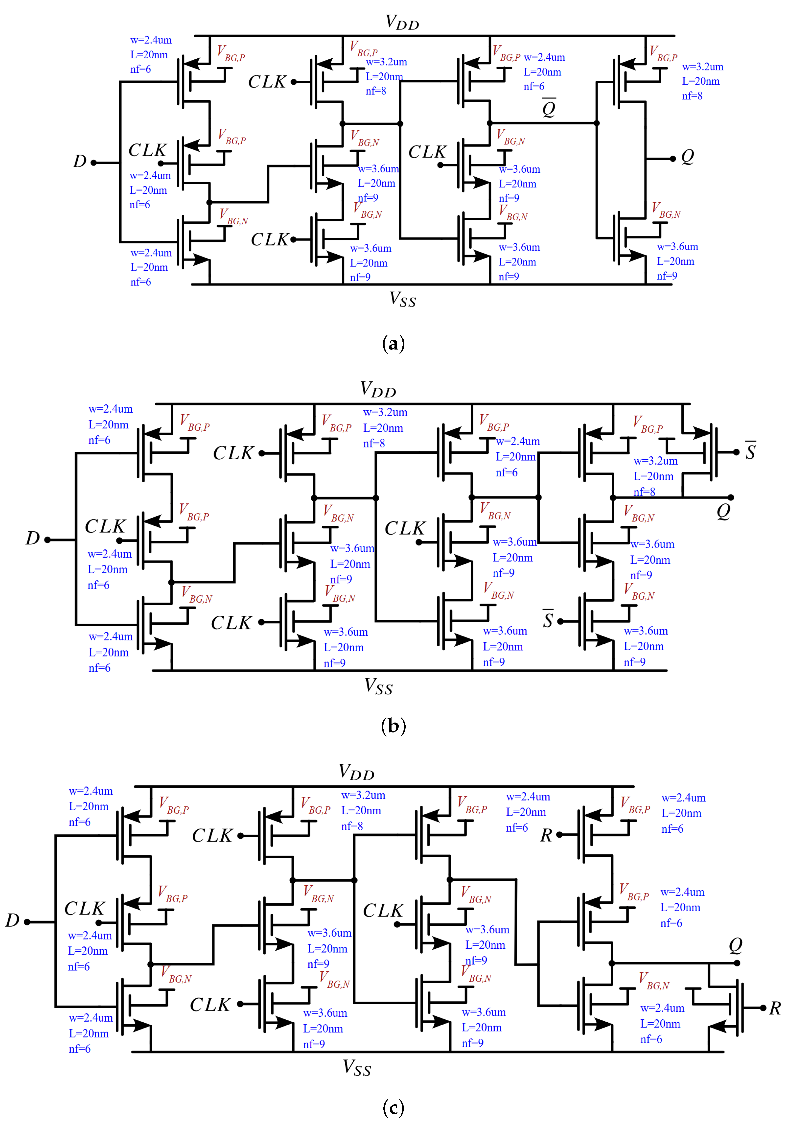
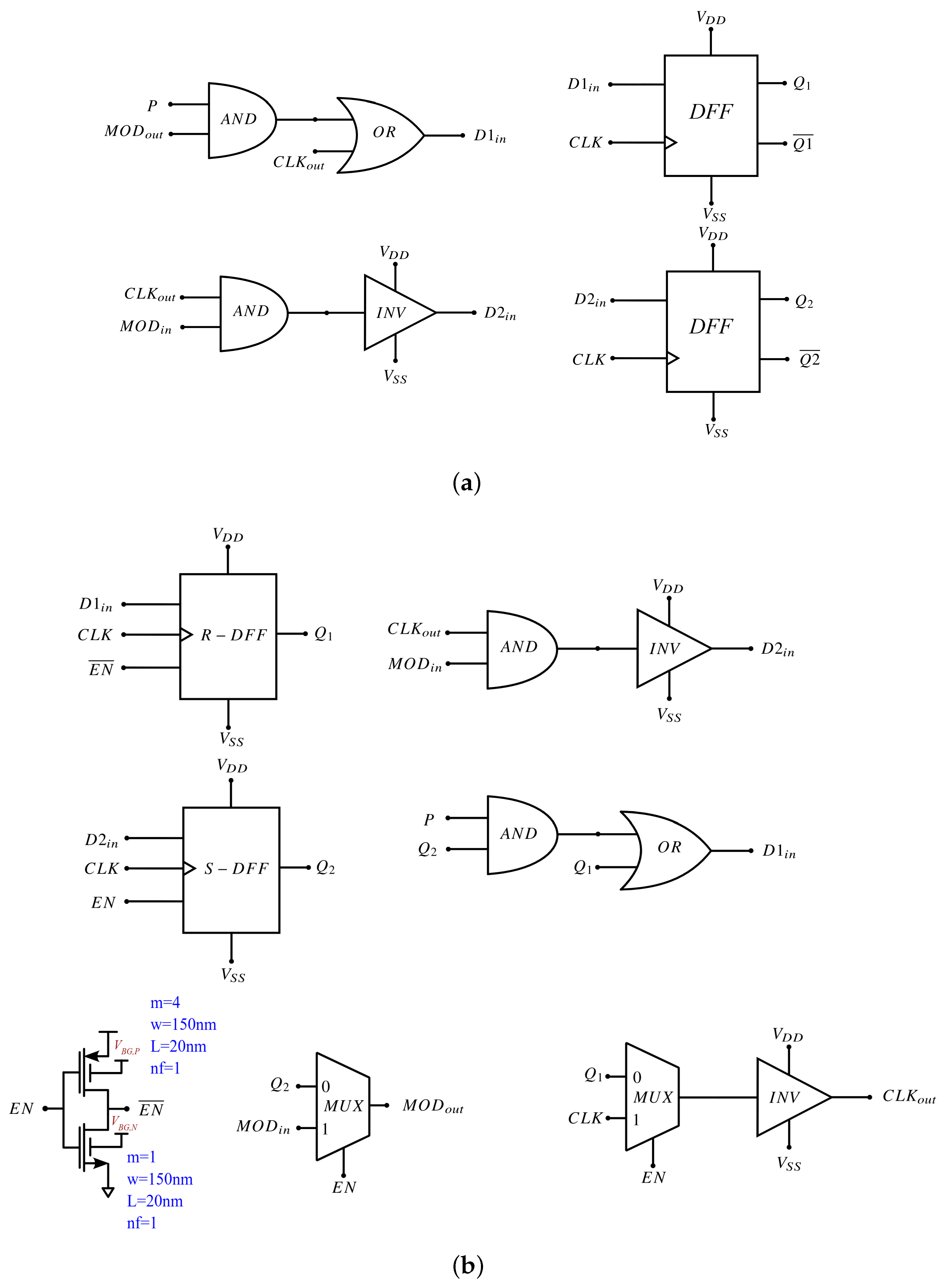
The speed and power of the chain are balanced across its six stages entirely with digital cells. The first two stages, which toggle at or near the full input rate, use higher-drive low-threshold (LVT) TSPC and static cells to meet the timing of the fastest node, while the later four stages use power-optimized regular- to high-threshold (RVT/HVT) static cells. The input clock reaches the first stage through a multiplexer that selects the divider input. The width, channel length, and finger count of every device are annotated on the schematics of Figure 2 and Figure 3, and the well configuration and back-gate rail of each stage group are summarized in Table 2.
Figure 2. Divider cell composition. The modulus AND function is implemented as a discrete gate ahead of the cell rather than merged into the master latch. (a) The 2/3 cell of the front high-speed stages: two clocked D flip-flops, shown at transistor level in Figure 3a, driven by the AND/OR/inverter modulus logic that selects between division by 2 and by 3. (b) The extended-range 1/2/3 cell of the later stages, which adds set and reset flip-flops (S-DFF, R-DFF) together with the enable multiplexers on the modulus and clock paths that force the stage transparent to realize the divide-by-1 mode; the back-gate pins of its enable inverter are labelled as in Figure 3 and assigned by Table 2.
Electronics 15 04036 g002
Figure 3. Transistor-level schematics of the flip-flops from which the cells are built, with the device width, channel length, and finger count annotated in blue and the back-gate terminal of every device drawn explicitly and labelled in red with its cell-level pin, V BG , N for an NMOS and V BG , P for a PMOS. The labels are net names rather than per-device connections: all devices of one polarity within a cell share a well, and therefore a single back-gate node, which is the rail the label names. (a) The clocked D flip-flop of the 2/3 cells. (b) The set flip-flop (S-DFF) and (c) the reset flip-flop (R-DFF) that generate the modulus-extension control for the divide-by-1 mode in the 1/2/3 cells. Because the front and later stages use opposite well configurations, the well and the rail behind each pin depend on the stage in which the cell is instantiated rather than on the cell; Table 2 gives that assignment and Figure 4a the corresponding cross-sections.
Electronics 15 04036 g003
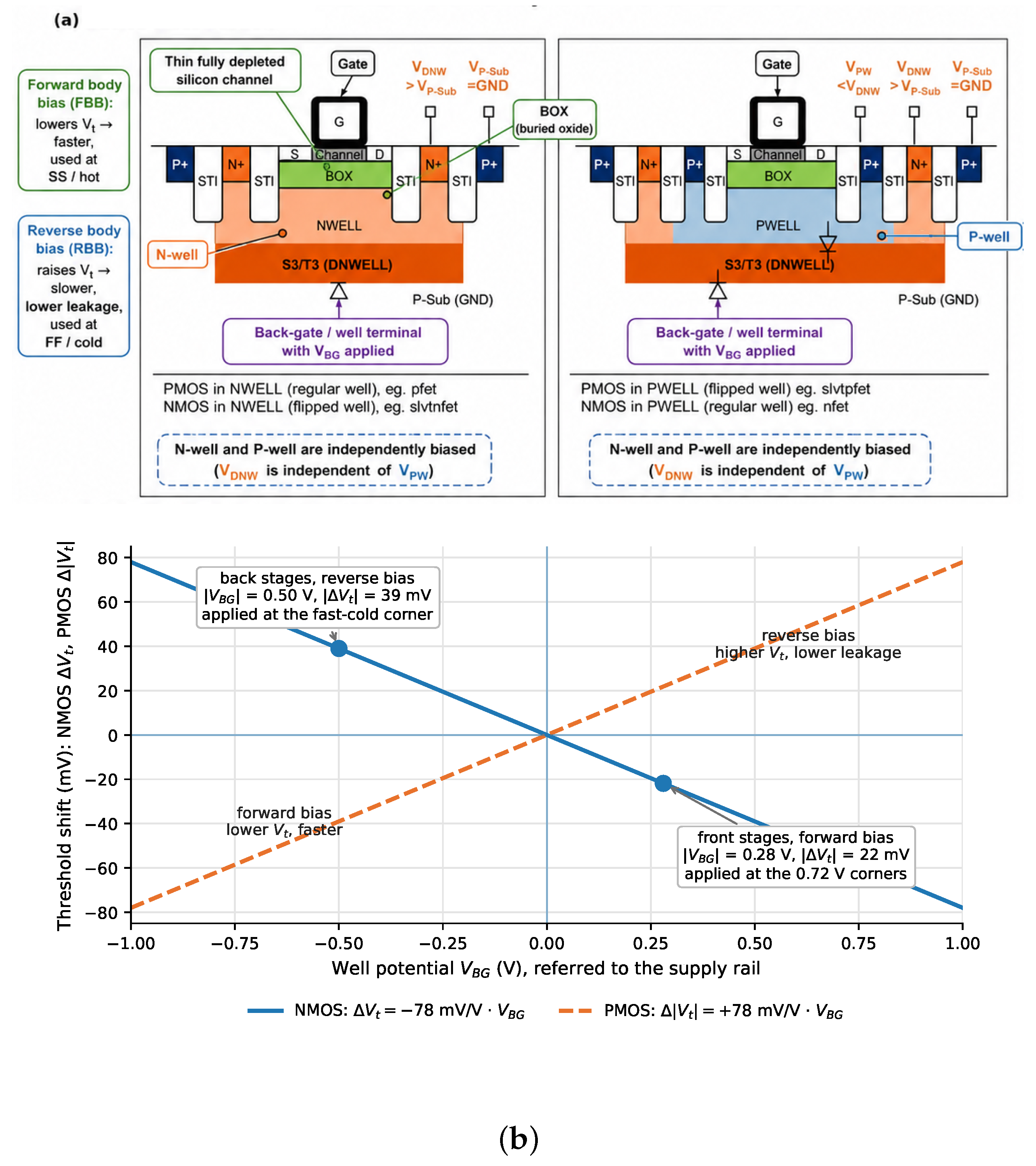
Figure 4. The FDSOI back gate as a continuous threshold-voltage knob. (a) Device cross-sections for the two well configurations: the buried-oxide back gate and the independently biased n-well and p-well, whose rails are labelled V DNW (deep n-well) and V PW (p-well) and which carry the bias values quoted in Section 2.5. Forward body bias lowers V t to speed the devices at slow corners, while reverse body bias raises V t at fast corners and rebalances the NMOS and PMOS edge rates. (b) Threshold shift against back-gate bias at a coupling of 78 mV/V, in the middle of the 70 to 85 mV/V range reported for the technology. The marked points are the well potentials actually applied in the extracted results of Section 3.5: 0.28 V on the front-stage rails at the 0.72 V corners and 0.50 V on the back-stage rails at the fast-cold corner. They are shown on the NMOS characteristic; the PMOS characteristic is its mirror image, so each point implies an equal and opposite excursion on the complementary rail.
Electronics 15 04036 g004

2.3. Flip-Flop and Modulus Logic

The high-speed first cell is composed of TSPC flip-flops, and the remaining cells of static D flip-flops, in each case with the modulus AND function realized as a discrete gate ahead of the master latch. Merging that function into the flip-flop itself, by embedding the modulus devices in the input network of the master latch, is an established technique for TSPC divider cells, and it removes a gate from the swallow path. A full NOR gate merged into the first flip-flop of a 2 / 3 prescaler is reported in [14,17]; it reduces that merge to a two-transistor swallowing network, lowering the node count on the critical path. That optimization is not applied in the present design, whose reported maximum frequencies are therefore obtained with the discrete-gate implementation; adopting it is a straightforward refinement for a future revision of the cell, at the cost of the wider devices needed to restore drive through the deeper series stack. The set and reset flip-flops generate the modulus-extension control that forces a stage transparent, realizing the divide-by-1 mode and the seamless range described above. Retiming of the modulus-control signal widens its timing margin, following the principle of [18]. In the present design the swallow path of each cell therefore comprises the two-input modulus AND, the OR that combines its output with the cell clock, and a single feedback inverter ahead of the master latch; the resulting modulus-control delay is contained within the available window at the target frequency, as confirmed by the functional verification of Section 3. The composition of the two cell types is shown in Figure 2, and the transistor-level flip-flops from which they are built in Figure 3.

2.4. FDSOI Back-Gate as a Design Knob

The divider is implemented in a 22 nm FDSOI process. A defining feature of this technology is the buried-oxide back gate, which acts as a continuous threshold-voltage control with a reported sensitivity of roughly 70 to 85 mV per volt of body bias and a usable range of about ± 2 V [9,11,19]. The nominal threshold of each device is first set by the well and device-type choice [20]. Forward body bias (FBB) lowers the threshold and speeds the devices, which recovers speed at slow corners, while reverse body bias (RBB) raises the threshold to slow the devices and recover leakage at fast corners [21,22]. Because the n-well and p-well are biased independently, the back gate also provides a direct means of rebalancing the relative strength of the NMOS and PMOS networks. The usable window depends on the well configuration: the LVT devices of the front stages are realized in the flipped-well configuration (NMOS above an n-well, PMOS above a p-well), which favors forward bias, whereas the RVT and HVT devices of the later stages use the conventional well configuration, whose window is mirrored toward reverse bias [11,20]. The compensation plan of Section 2.5 respects these windows: forward bias is applied to the flipped-well front stages at the slow corners, reverse bias to the conventional-well later stages at the fast corners, and the flipped-well devices are returned to zero back-gate voltage where a reverse bias would exceed their small permitted range. Figure 4 illustrates the knob.

2.5. Three-Method PVT Compensation Scheme

The timing margin that the all-digital implementation gives up relative to CML is recovered by a layered scheme that proceeds from a global knob to a local one to a systematic one.
The three layers are not three independent knobs, and it is worth stating their division of labor before describing them individually. Method 1 acts on the devices through the back gate; it is the only layer that changes the internal clock duty cycle, and it is therefore the layer that closes the duty-collapse failure mode. Method 2 is the physical trim hardware, namely the programmable delay cells placed on the timing-critical stages. Method 3 is not additional hardware but the systematic procedure that chooses the codes those cells are given; Methods 2 and 3 consequently share the same registers and are applied as one code assignment rather than as two independent corrections. In the compensated design the codes are set by the Method 3 projection, which minimizes the accumulated timing error of the chain as a whole rather than centring any single path; the swallow-path timing that this leaves uncentred is then carried by the margin that Method 1 restores. The methods are thus complementary by construction: Method 1 supplies margin and duty balance, and Methods 2 and 3 supply accuracy within that margin.

2.5.1. Method 1: Back-Gate Body Bias (Global)

The back gate is used as a global PVT knob, and it acts differently at each of the three failing corners. At the slow corners, where the swallow path evaluates too slowly and the data misses the next clock edge, forward body bias speeds the logic and restores the setup margin. At the fast-cold corner (FF, 0.88 V, 40   ° C), where the data races through before the latch has settled, reverse body bias slows the path and restores the hold margin. At the skewed corners (SF and FS), where the NMOS and PMOS edge rates diverge and the collapsing internal duty cycle erodes the precharge and evaluate windows of the TSPC front cell, biasing the two wells by different amounts rebalances the edges. Body-bias compensation of process and temperature spread in 22FDX is well established for digital and mixed-signal blocks [10,22,23,24]; the complete compensation of corner and temperature dependence in a 22FDX oscillator is a direct precedent [9], and back-gate control of a 22 nm FD-SOI divide-by-four prescaler has been demonstrated in silicon [12,13].
The rails that carry these biases follow from the well structure of Section 2.4. In the flipped-well front stages the NMOS body lies above the deep n-well and is controlled by V DNW , while the PMOS body lies above the p-well and is controlled by V PW ; in the conventional-well later stages the two assignments are exchanged. The two groups are not biased alike at a given corner since their permitted windows differ, so they cannot share one pair of wells. The front stages therefore carry their own rail pair, V DNW , F and V PW , F , and the later stages a separate pair, V DNW , B and V PW , B : four independently driven back-gate nets in all. On the schematics of Figure 2b and Figure 3 each back-gate terminal is drawn explicitly and labelled with its cell-level pin, V BG , N for an NMOS and V BG , P for a PMOS, because which of the four rails an instance connects to is set by the stage it is placed in rather than by the cell. Table 2 gives that binding so that every transistor in the figures can be traced to the rail that drives it and, through the cross-sections of Figure 4a, to the well that rail biases. The delay-trim cells of Method 2 belong to none of the four nets and are held at a fixed back-gate potential, which keeps the two knobs independent.
The quantity actually programmed is the potential of the well itself. In FDSOI the back gate of a device is the well beneath the buried oxide, so every device sharing a well shares one back-gate node, and within a cell all the devices of one polarity therefore sit on a single rail, as Figure 3 shows. Forward and reverse bias denote driving that rail in the direction that respectively lowers and raises the threshold of the devices above it, and the values quoted here are well potentials referred to the supply rail of the corresponding polarity. Because some devices sit in series stacks, their source is at an internal node rather than at the supply, so the body-to-source bias they see, and with it the threshold shift they receive, is somewhat smaller than for a device whose source is at the rail; the coupling quoted in Section 2.4 refers to the latter case. In the extracted results of Section 3.5 the applied forward bias reaches 0.28 V on the front-stage rails at the 0.72 V corners, and a reverse bias of 0.50 V is applied to the back-stage rails at the fast-cold corner; both are well inside the safe range of the technology and the per-flavor windows of Section 2.4. The rebalancing at the skewed corners is visible in the same table as an asymmetry between the two front-stage rails, + 0.18 and 0.12 V at SF and the mirror-image pair at FS, according to whether the PMOS or the NMOS edge is the slower one. Forward body bias in FDSOI does not degrade device reliability and adds only a bounded junction leakage that remains small relative to the dynamic current at the operating frequency [21]. The bias values are applied as a one-time, per-corner setting; a closed-loop controller that senses an on-chip timing monitor and sets the bias could be added with the small area and power overhead reported for 22FDX back-bias regulators [22,23], and is left to future work.

2.5.2. Method 2: Per-Stage Programmable Delay Trim (Local)

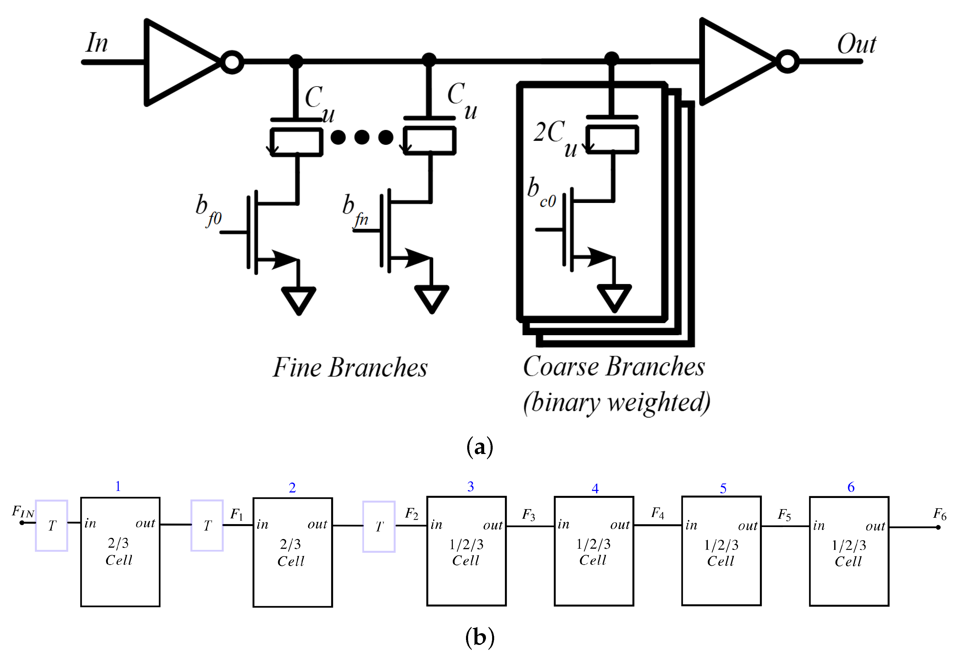
The second layer is local: a digitally programmable delay trim on the timing-critical stages, built from a 0.10 μ m/20 nm RVT unit cell, equalizes the stage-to-stage path delays and recenters the timing of the swallow/AND critical path that limits the maximum frequency. Each trimmed stage carries a coarse and a fine trim code. The cell is a digitally controlled shunt-capacitor delay element: the inter-stage path is buffered at full strength, the delay is set by switching capacitors onto the internal node, and a second inverter restores the edge rate before the path continues, with unit capacitors on the fine branches and binary-weighted ones on the coarse branches, as shown in Figure 5a. This topology is preferred here over a current-starved inverter or a variable-drive array because it dissipates only the switching energy of the capacitors actually selected, draws no static current, and leaves the driver at full strength so that the edge rate, and with it the sensitivity of the following stage, is not degraded by the trim. Selective tuning of only the timing-critical elements follows the philosophy of clustered compensation [25], and the coarse–fine arrangement mirrors common digital calibration practice [26]. The same trim cells provide the correction vectors { δ k } used by the systematic trim of Method 3, which sets their code width and quantifies the achievable residual. Here δ k denotes the change produced in the chain’s timing-error vector when the trim code of stage k is advanced by one coarse step, with all other codes held fixed, measured at the critical flip-flop; it is extracted at the same corner at which the timing-error vector itself is reported, SS at 0.72 V and 125   ° C, so that the correction subspace and the error it is projected against belong to one operating point, and the extracted step is 1.05 ps per coarse code step, the fine step being 0.13 ps. It is a vector with one component per stage rather than a scalar delay, because a code step on one stage also perturbs the edge timing seen by the others.

2.5.3. Method 3: INL Trim and the Error-Span Limit (Systematic)

The final layer is a systematic trim that targets the accumulated, integral-nonlinearity-like timing error across the chain, in the spirit of integral-nonlinearity background calibration of dividers [27]. Each trimmed stage k carries a B-bit code c k , with B = 6 split as a three-bit coarse field and a three-bit fine field, so that the stage spans 2 B delay settings, and the applied correction is k c k δ k , where c k is a signed integer over that stage’s code range. The codes are multi-level rather than binary selectors so that a stage’s correction is an integer multiple of its delay step rather than a single on/off increment. Within that range the correction can reach any point of span { δ k } up to the quantization step, so what limits the achievable accuracy is not the number of codes but the component of the error lying outside that span. Writing the true error e for the vector of per-stage swallow-path timing deviations defined below, the residual is the projection of e onto the orthogonal complement of span { δ k } ,
e res = I P e , P = projector onto span { δ k } .
The error vector is defined as follows: its components are the per-stage swallow-path timing errors, that is, the deviation of each stage’s modulus-window edge from its nominal position at the critical flip-flop, obtained from a post-layout transient at the target frequency, so that e has one component per stage of the six-stage chain. Each basis vector δ k is characterized once per corner by stepping trim code k alone and recording the resulting change in e.
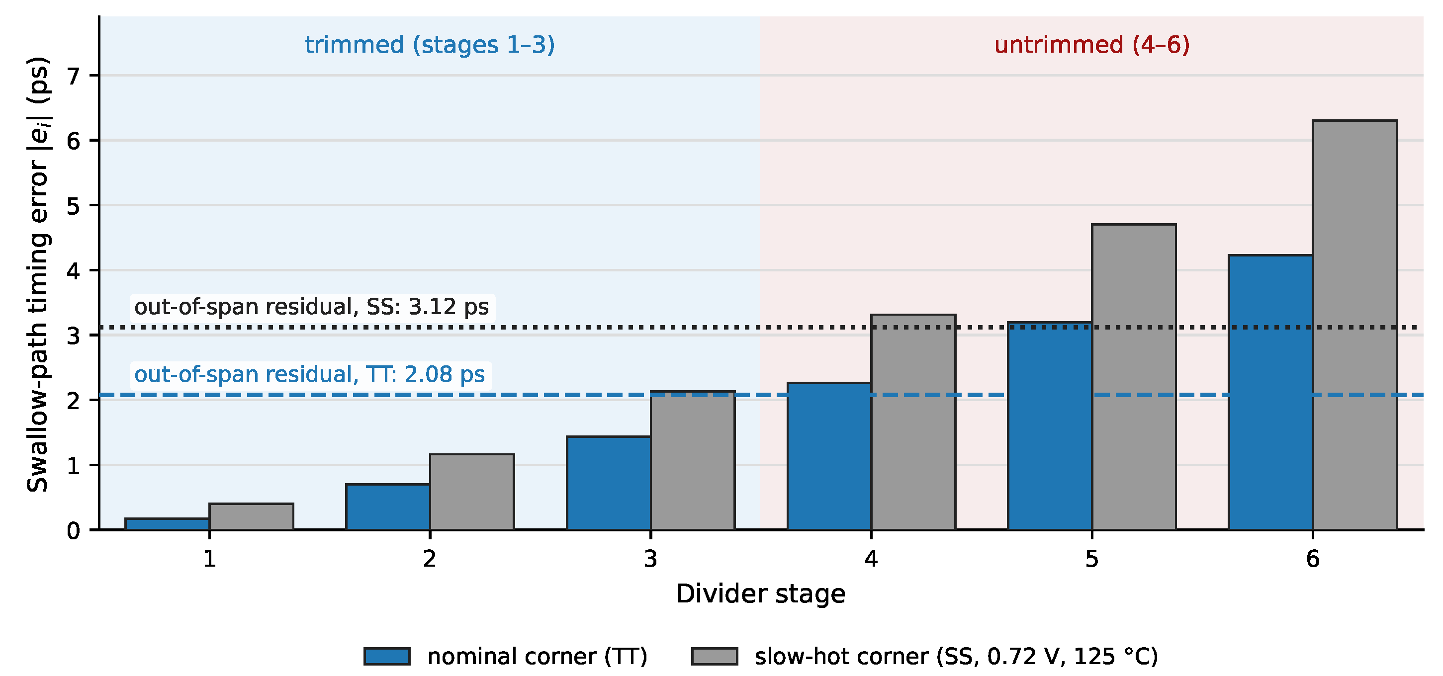
The delay trim is placed only on the timing-critical stages 1–3, the three fastest stages of the cascade, which set the maximum frequency, and not on the divided-down back-end stages 4–6, which self-clean through their divider flip-flops. The correction subspace span { δ k } is therefore a strict subspace of the six-dimensional error space, of dimension three when stages 1–3 are trimmed. It is not, however, confined to the trimmed stages. Because the output of stage k is the clock of stage k + 1 , and the trim cells are delay elements inserted in that inter-stage path, advancing a trim code displaces the modulus window of the trimmed stage and of every stage downstream of it by the same amount. The correction subspace therefore contains the common-mode component of the untrimmed back-end errors, and only their relative spread lies in the orthogonal complement. The residual does not vanish, but neither is it the root-sum-square of the untrimmed-stage errors: it is the norm of the orthogonal projection itself,
e res = ( I P ) e .
Table 3 gives the post-layout per-stage error vector at the nominal and slow-hot corners, extracted from transient simulation at the target frequency. The error accumulates monotonically along the chain, as expected of a cascade in which each stage inherits the edge displacement of its predecessor. The trim cancels the errors of the trimmed stages and, through the inter-stage coupling described above, also cancels the common-mode component of the back-end errors; what survives is the spread of the back-end errors about that common value. The resulting residual is 2.08 ps at the nominal corner and 3.12 ps at the slow-hot corner (SS, 0.72 V, 125   ° C), as Figure 6 shows. These residuals are the floor the correction reaches when the three stage codes are set independently, which is what gives span { δ k } its dimension of three. The corner runs of Section 3.5 apply a single shared code word to the three trimmed stages, which confines the applied correction to a one-dimensional line within that subspace, so the residual realized at those points is no smaller than, and in general exceeds, the values above. They are the achievable limit of the method rather than the value realized at every tabulated corner. The conclusion the decomposition demonstrates, that the achievable accuracy is set by the uncorrected error subspace and not by the number of trim codes, does not depend on the particular values.
As a corollary, trimming every stage would make span { δ k } the full space and drive the delay residual to zero; the floor would then be set not by delay but by the non-delay part of the error, the duty-cycle and edge-rate skew that a delay trim cannot represent, which for this design is about 0.6 ps. This is why the systematic trim is framed as an error-span limit rather than as an arbitrarily improvable knob. Because the codes are quantized, a quantization residual also exists; with the measured 0.13 ps fine step it contributes the step divided by 12 , about 0.04 ps, in quadrature, which is negligible against the out-of-span component, so the residual reported above is a timing-error floor and not a code-resolution limit. The trade-off between correction speed and accuracy is discussed in [28].
A dedicated duty-cycle correction block is not used. Because the application does not require a 50% output duty cycle, the duty-cycle behavior at the skewed corners is treated as a robustness property that Method 1 restores, rather than as a specified output feature. If a 50% output were required, the all-digital duty-cycle correctors of [29,30,31] would be the natural addition; they are cited for completeness but not used here.

3. Results

3.1. Verification Methodology

All results in this work are obtained by simulation; no silicon is measured. The flow is designed to be reproducible and to approximate measurement as closely as possible. The design is characterized over the PVT box formed by the process corners { SS , FF , SF , FS } , supply voltages { 0.72 , 0.80 , 0.88 } V, and temperatures { 40 , 27 , 125 } ° C, giving the 45-point matrix of Table 4; the temperature axis of the verification flow is these three temperatures at every corner and supply. The temperature dependence is not monotonic across the supply range: at 0.72 V the chain becomes faster as it heats and at 0.88 V slower, which is the zero-temperature-coefficient behavior set out in Section 3.5. Each block is simulated first at the schematic level and then after layout with extracted parasitic resistance and coupling capacitance so that all reported performance is post-layout; the layout parasitics are extracted with Siemens Calibre, after design-rule (DRC) and layout-versus-schematic (LVS) checks, in RC-coupled mode. Transient and timing simulations use Cadence Spectre, and phase noise and jitter use the periodic steady-state (PSS) and periodic-noise (PNoise) analyses of SpectreRF. The reported quantities are the maximum operating frequency, the setup and hold margins, the internal clock duty cycle, the additive jitter and phase-noise floor, and the average and peak supply current with the energy per cycle. Robustness is assessed over the corner box defined above and, for random process and mismatch variation, by the paired Monte Carlo campaign of Section 3.8. The technology is the GlobalFoundries 22FDX (22 nm FDSOI) process.
The power of the all-digital divider is compared with current-mode logic through two arguments with deliberately different roles. The first is mechanistic: an analytical lower bound on the CML bias current that shows how that current arises and how it scales with frequency. The second is empirical: a magnitude comparison against the measured power of published CML dividers. Only the second supports the numeric efficiency figure; the analytical bound is used to characterize the nature of the CML supply current, not to claim that the all-digital design draws less power than an idealized CML latch. No CML reference was designed in this work, so the magnitude comparison cannot be biased by a self-chosen baseline; the absence of a same-node CML anchor is discussed as a limitation in Section 4. A CML latch develops a logic swing Δ V across a load resistor R L and must resolve it within the bit period. Settling at frequency f requires the output pole to satisfy 1 / ( 2 π R L C L ) f , hence R L 1 / ( 2 π f C L ) with C L the latch load; combined with the swing condition Δ V = I tail R L , this bounds the tail current of each latch from below,
I tail , min = 2 π f C L Δ V .
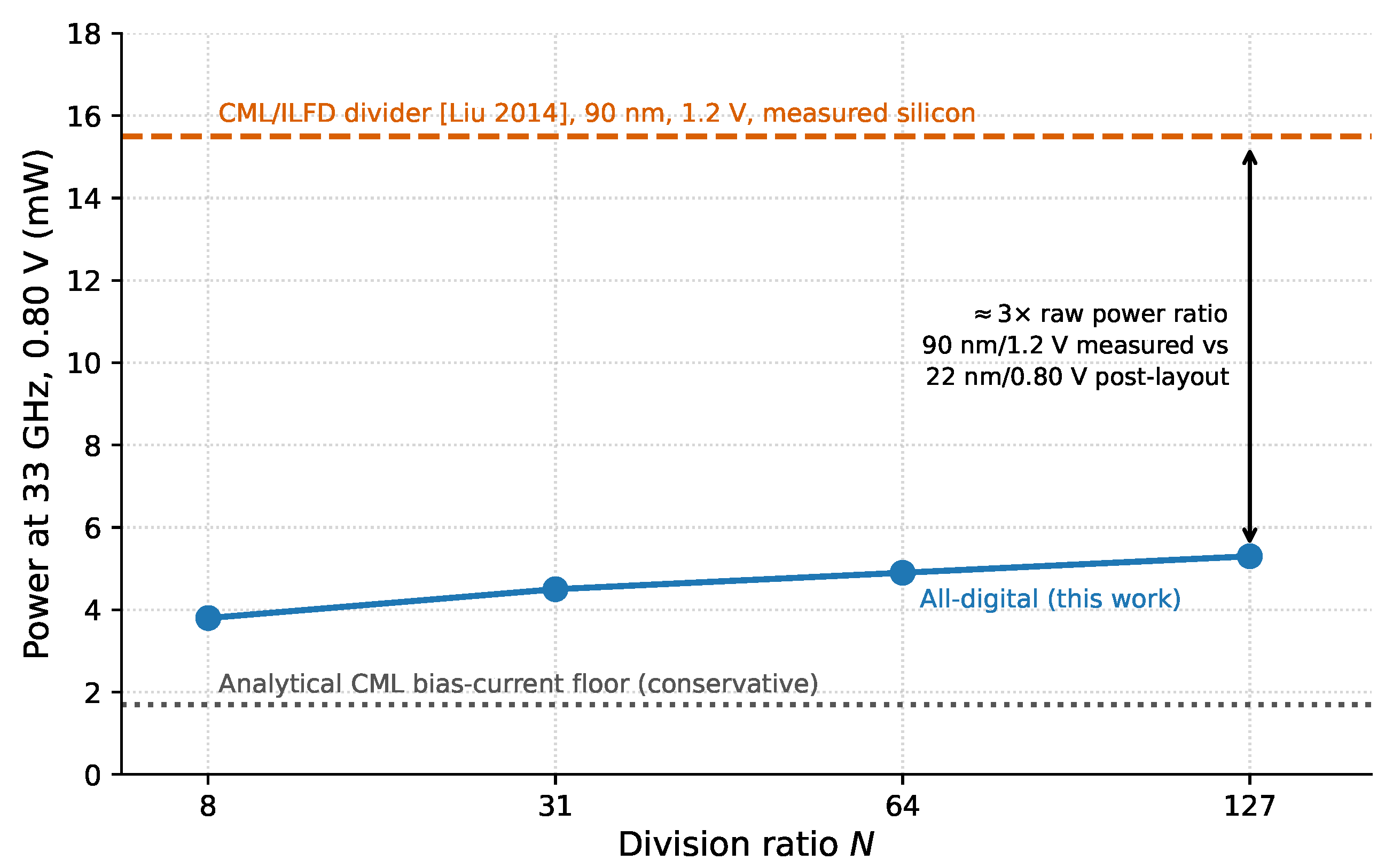
Since CML latches regenerate rather than settle fully, Equation (5) is a conservative settling-based floor rather than an exact limit. The essential difference is qualitative: this bias current grows linearly with the operating frequency and is drawn continuously, independently of activity, whereas the static-CMOS chain draws only dynamic current that scales with activity, plus leakage, and falls at low division ratios where fewer stages are active. Numerically the bound is deliberately small: for a latch load C L = 10 fF and a logic swing Δ V = 250 mV at the 33 GHz target, it evaluates to 0.52 mA per latch, so a four-latch high-speed front end is bounded below by only about 2.1 mA, or 1.7 mW at 0.8 V, which is itself below the simulated supply current of the all-digital divider. This is expected, and it is why the bound characterizes the mechanism rather than the magnitude. Equation (5) bounds the irreducible bias term alone. The realized power of a current-mode divider is instead set by the practical overheads of the style: the swing margin, the device sizing needed for gain and matching, the output buffering, and the always-on bias. For published CML and BiCMOS dividers at comparable speed these reach tens of milliwatts [3,4,5]. The efficiency comparison therefore rests entirely on the measured power of these published designs, normalized by a power-efficiency figure of merit, and the all-digital jitter is reported so that the comparison is not confounded by an unstated noise penalty. The bound is illustrated in Figure 7.

3.2. Layout and Area

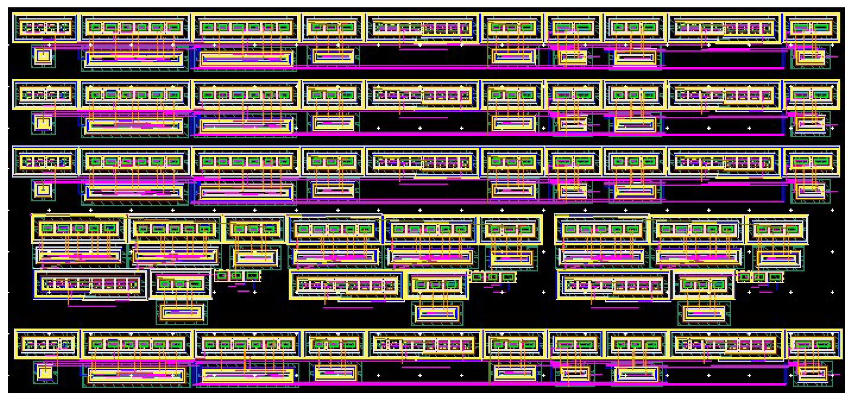
The divider was laid out in the 22 nm FDSOI process, and all reported results are extracted from this layout. The core occupies 100 × 50 μ   m 2 , that is 0.005   mm 2 , excluding pads, which reflects the compactness of an all-digital realization that needs no bias network or large current-mode devices. Figure 8 shows the core layout.

3.3. Functional Verification

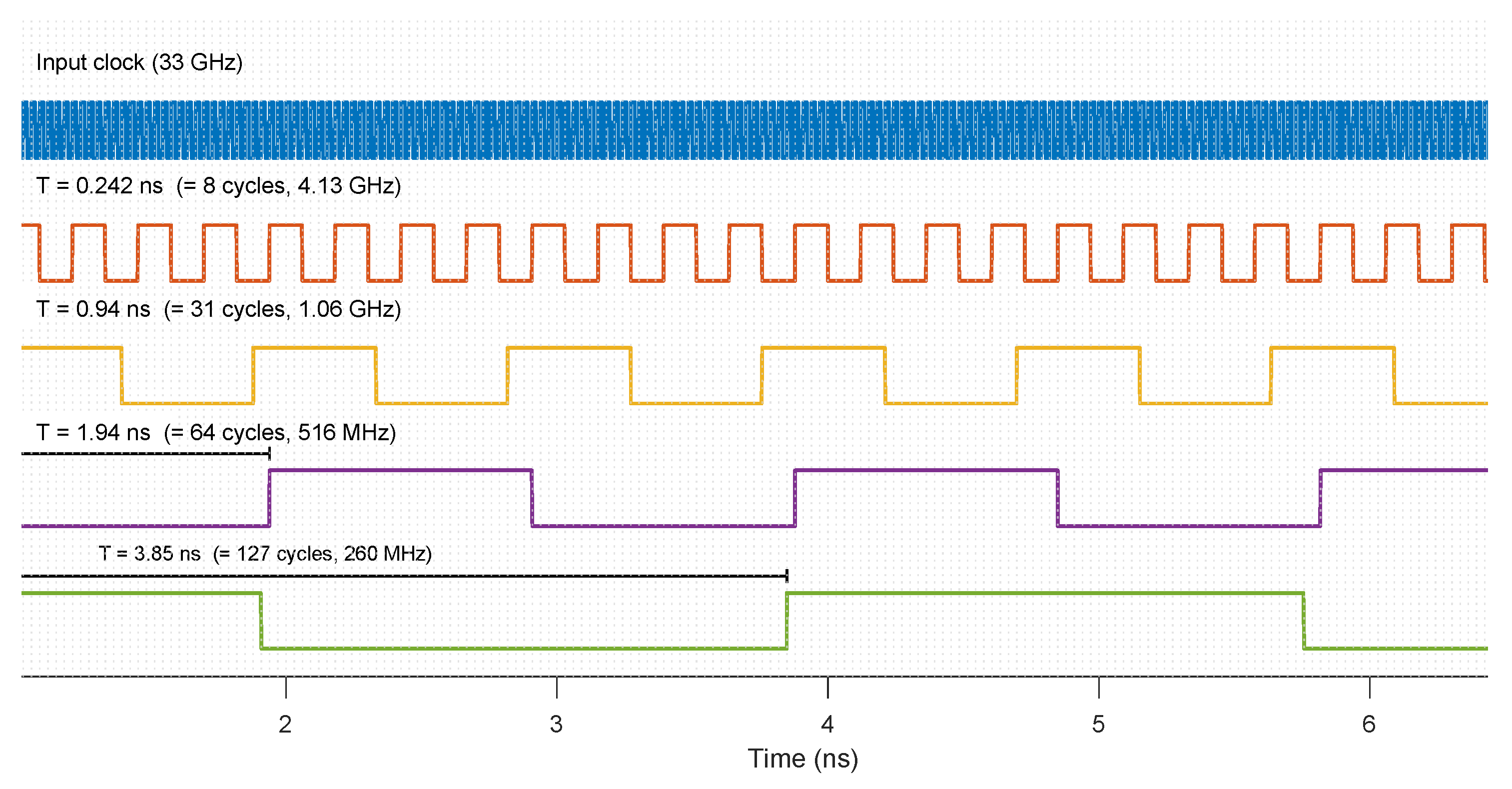
Correct division is confirmed at N = 8 , 31 , 64 , 127 and across the full programmable range. At the 33 GHz input these ratios produce output frequencies of 4.13 GHz, 1.06 GHz, 516 MHz, and 260 MHz, respectively, with no missing or extra cycles observed over 10 4 input periods at the typical corner. Figure 9 shows the input clock and the divided outputs.

3.4. Operating Range and Input Sensitivity

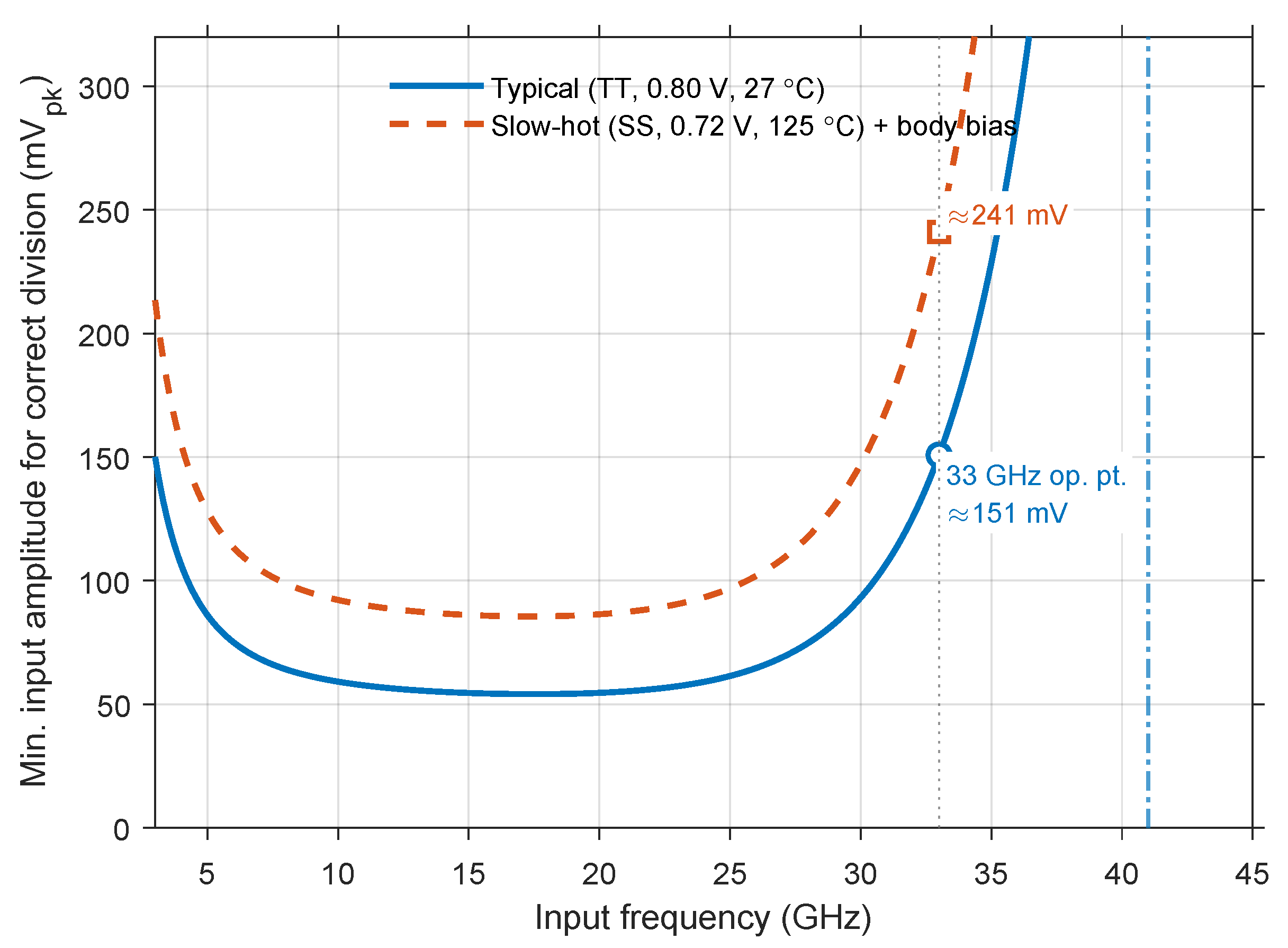
Because the first cell processes the full 33 GHz input directly, the self-oscillation and input-sensitivity behavior of the TSPC front stage set the practical operating range. Figure 10 shows the minimum input swing required for correct division as a function of input frequency. At the typical corner the front cell divides correctly up to 41 GHz, its toggle limit, which lies above the 39.5 GHz maximum frequency of the complete chain in Table 4. The minimum input amplitude there is 151 mV at 33 GHz. Input amplitudes in this section and in Figure 10 are quoted as peak values of the sinusoidal input. At the slow-hot corner the requirement rises to 241 mV, but the divider still captures the 33 GHz input once body bias is applied, consistent with the input sensitivity reported for modular 2/3 chains [1]. Without body bias the slow-hot corner cannot capture the 33 GHz input at any amplitude, consistent with its uncompensated maximum frequency of 30.5 GHz in Table 4; the compensated curve of Figure 10 therefore shows a margin that Method 1 creates.
The sensitivity curves are U-shaped, and the rising branch at the low-frequency end is worth identifying because it bounds the divider from below. The results reported here hold the input at 33 GHz and let the output move with the division ratio, which characterizes the divider as a standalone block at its speed-limiting condition. In a synthesizer with a fixed reference the convention is inverted: the output is pinned to the reference and the input frequency moves with N, so a small ratio corresponds to a low input frequency. The limit that a low input frequency threatens is not the setup, which relaxes as the clock period grows, but the charge retention. The front cell is TSPC and its internal nodes are dynamic, so at a sufficiently low frequency their stored charge droops through subthreshold and junction leakage before the next evaluate phase, most severely at the hot corner where that leakage is largest. The all-digital chain therefore has a minimum as well as a maximum operating frequency, and it is the low-frequency branch of Figure 10, rather than the high-frequency one, that governs operation at small N.
That limit was quantified by sweeping the input frequency and amplitude at the corner where leakage is largest, FF at 0.88 V and 125   ° C, with the front-cell dynamic node probed directly. Two mechanisms are separable there, and they are distinguished by repeating the failing points with a fast-edged square wave of the same amplitude. The first is the charge droop itself. Measured droop scales inversely with input frequency, as retention on a dynamic node must, giving a droop-frequency product of about 19.5 mV·GHz at this corner and hence a leakage-limited minimum frequency of roughly 222 MHz against a droop budget of a tenth of the supply. Between 27 and 125   ° C the droop rises by a factor of 3.75 , a weaker temperature dependence than subthreshold conduction alone would give.
The second mechanism binds first, and it is not a property of the divider’s storage nodes. Below an input slew rate of about 0.47 V/ns, taken at the zero crossing and equal to π f V pp for a sinusoidal input, the crowbar current drawn while both clocked devices conduct through the input transition prevents the precharge node from establishing, and the cell fails while its droop is still well inside budget. The threshold is a function of slew alone rather than of frequency or amplitude separately. At fixed frequency the cell divides correctly down to 150 mV of input swing and fails at 120 mV; the same slew reached instead by lowering the frequency at constant amplitude fails identically; and restoring the edge rate with a square-wave input of the same amplitude recovers correct division at every point tested. Consistently with the crowbar mechanism, the requirement is more severe at the fast corner, where the devices are strongest, than at the slow corner.
The practical consequence is favourable. At the N = 8 operating point of the fixed-reference plan, an input of 2.08 GHz, the slew requirement corresponds to an amplitude of about 36 mV peak, that is 72 mV peak-to-peak, whereas the front cell already requires 151 mV peak at 33 GHz for the high-frequency limit of Figure 10. The drive that the high end of the range demands therefore exceeds the low-frequency requirement by about a factor of four. The divider is bounded from below by an input-interface specification, a minimum slew rate to be met by the buffer that drives it, rather than by an intrinsic retention limit of its own nodes; the retention limit lies almost an order of magnitude below the lowest input frequency the division range calls for.

3.5. Maximum Operating Frequency over PVT

The post-layout maximum operating frequency was extracted across the PVT corner box, both with the back-gate compensation of Method 1 disabled and enabled. The criterion is stated explicitly since a maximum frequency is only meaningful with one: f max is the highest input frequency at which the complete six-stage chain divides correctly in a post-layout transient, correctness being evaluated over a settled output interval at the critical flip-flop, at the division ratio and input amplitude quoted with the table. It is a transient-verified toggle limit rather than an extrapolation from a timing arc. The results are summarized in Table 4. Without compensation the slow and skewed corners fall below the 33 GHz target at 0.72 V: the slow-process corner reaches only 29.8 to 30.5 GHz and the two skewed corners 30.5 to 32.0 GHz, which is the origin of the setup failure analyzed in Section 3.6. The typical and fast corners clear the target at this supply without compensation, reaching 34.5 to 35.2 GHz and 42.5 to 45.0 GHz respectively, so the low supply alone is not sufficient to cause the failure: it requires the slow or skewed process corner as well. With the per-corner body bias applied, every corner is held at or above the target, the tightest being 33.0 GHz. At the fast-cold corner, the limitation is hold rather than speed; there, the reverse bias deliberately trades the excess speed of the corner ( 51.0 GHz to 46.5 GHz in Table 4) for the hold margin restored in Section 3.6. The two corners are therefore limited by different mechanisms. The worst-case operating condition is the cold corner at the low supply, FS at 0.72 V and 40   ° C, where the maximum frequency is limited to 33.0 GHz; the neighboring SS corner at the same supply and temperature reaches 33.2 GHz. At the cold corner the threshold voltage is high enough that even the applied forward bias leaves the TSPC front cell only just able to resolve the 33 GHz input, and the compensated margin over the target is correspondingly small.
The hot corner at the same supply is not the worst case, which is worth stating because it inverts the usual expectation. At SS, 0.72 V and 125   ° C the maximum frequency improves to 35.0 GHz: at this supply the design operates near the zero-temperature-coefficient point, where the fall of the threshold voltage with temperature outweighs the loss of carrier mobility, so the chain becomes faster as it heats. The consequence for the compensation plan is that the binding condition is cold rather than hot at 0.72 V, and the forward bias must be sized for the cold corner. The higher figure at the fast-cold corner is not a better operating point but a different constraint, hold rather than speed.

3.6. Failure-Mode Analysis and Closure

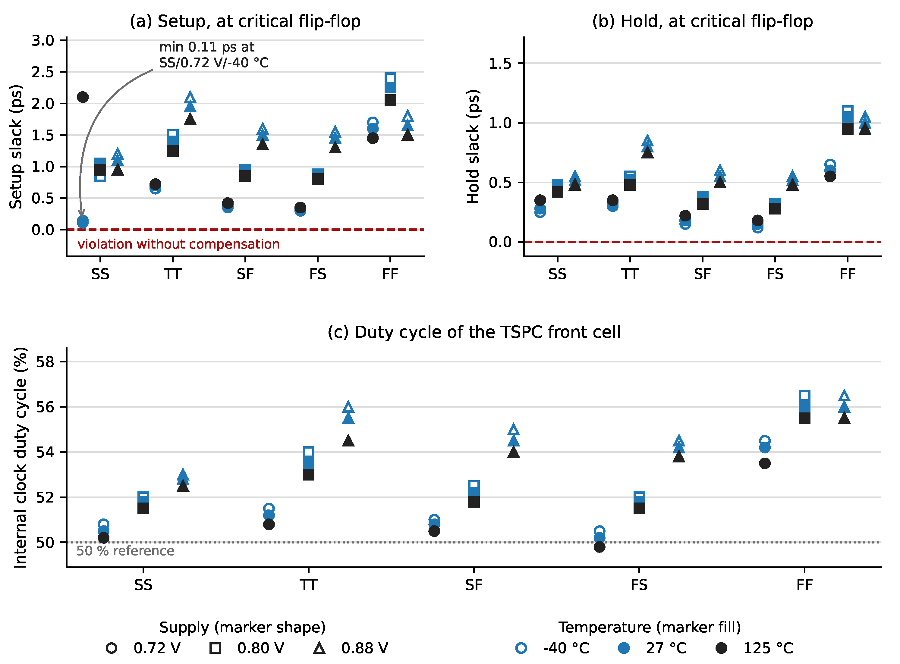
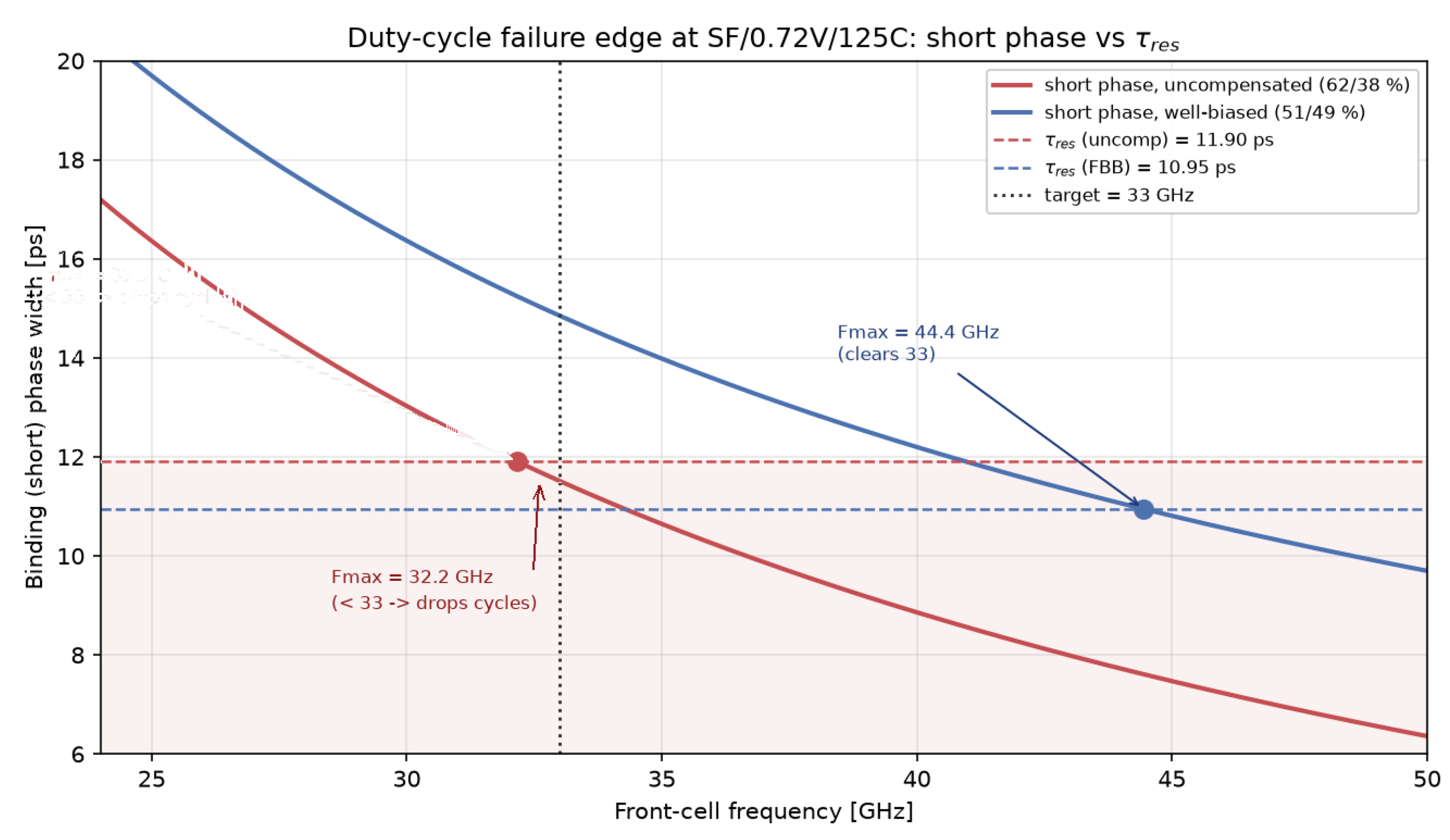
Each of the three PVT failure modes is shown first as a violation and then closed by the corresponding method, as summarized in Table 5 and illustrated in Figure 11. At the slow-hot corner the setup slack is negative before compensation and is restored to a positive value by forward body bias. The restored margins are small in absolute terms: the extracted post-layout system-level setup slack at the critical swallow-path flip-flop, which includes the clock-tree insertion delay and the chain output edge, ranges from + 0.11 ps at the cold low-supply corner to + 2.40 ps at the fast-cold corner across the whole box. At the fast-cold corner the hold slack, measured on the same basis as the setup slack but against the earliest rather than the latest permitted data arrival, is negative before compensation and is restored to a positive value by reverse body bias. At the skewed corners the internal clock duty cycle collapses to 62 / 38 % and is rebalanced to 50.5 / 49.5 % by independent well biasing; across the supply and temperature extremes of the corner box the rebalanced duty at the two skewed corners stays within 49.8 to 55.0 % (Table 4, Figure 11c). This collapse is a genuine functional failure at the corner extreme, not merely a loss of margin. At the worst skewed corner (SF, 0.72 V, 125   ° C) the 62 / 38 % duty narrows the binding, short evaluate phase of the TSPC front cell to 11.51 ps, below the front-cell resolve time τ res 11.90 ps needed at 33 GHz, a deficit of 0.39 ps; the front cell then drops and inserts cycles, and its reliable divide frequency falls to 32.2 GHz, below the target. Independent well biasing widens the binding phase to 14.85 ps and, through the accompanying forward bias, lowers τ res to 10.95 ps, lifting the front-cell limit to 44.4 GHz and restoring correct division, as Figure 12 shows. That the mechanism is duty skew rather than raw slowness is confirmed by the symmetric slow corner SS ( 0.72 V, 125   ° C). That corner is equally slow in supply and temperature, but its duty stays near-balanced at 50.2 / 49.8 % and it still divides correctly to 35.0 GHz (Table 4), above the target. It is therefore the NMOS/PMOS edge-rate asymmetry of the skewed corners, not the reduced device speed, that erodes the evaluate window. The resolve-time and edge-skew magnitudes used here are representative values consistent with the simulated 62 / 38 % duty, and the mechanism does not depend on their exact size. The slack values are extracted from the data and clock waveforms at the critical swallow-path flip-flop. The maximum frequencies of Table 4, by contrast, come from transient simulation of the complete chain and are set by the worst mechanism at each corner. The two characterizations are therefore related but not arithmetically interchangeable: a negative slack is measured against the required setup window of the flip-flop rather than against outright functional failure, and after compensation the chain is limited by the next-worst mechanism rather than by the corrected path.

3.7. Contribution of the Individual Methods

The three methods act on different quantities, so their contributions are reported separately and in the units each one governs, rather than combined into a single figure of merit.
Method 1 is isolated directly by the paired columns of Table 4, which give the maximum operating frequency at each point with the back-gate compensation disabled and enabled and are otherwise identical runs. Where forward bias is applied it contributes between + 1.3 and + 4.5 GHz, the largest gains falling on the slow-process corners that fail without it and the smaller ones on the skewed corners, where the bias is asymmetric and is spent on rebalancing the edges rather than on speed alone. At the typical corner the contribution is zero since no bias is applied there. At the fast-cold corner the sign reverses by design: reverse bias on the back-stage rails costs between 1.0 and 14.5 GHz of maximum frequency, the largest reduction occurring at 0.88 V where the back-stage race is tightest, and buys the hold margin of Table 5. That this cost is a deliberate trade rather than a loss of capability is clear from the uncompensated column, which reaches 61.0 GHz at that corner with no usable hold margin. Method 1 is also the only layer that acts on the internal duty cycle, moving it from 62 / 38 % to 50.5 / 49.5 % at the skewed corner, and the only one that closes the setup and hold violations, restoring both to positive extracted slack ( + 2.10 ps and + 1.05 ps at the respective corners of Table 5).
Methods 2 and 3 are reported jointly because they are not separable by construction. Method 2 is the trim hardware and Method 3 is the procedure that selects the codes those cells are given; the two share the same registers and are applied as a single code assignment, so a contribution attributable to the hardware independently of a code choice is not a defined quantity. What they jointly make achievable is the reduction of the accumulated timing error from the norm of the uncorrected error vector of Table 3, 5.98 ps at the nominal corner and 8.89 ps at the slow-hot corner, to the out-of-span residual of 2.08 and 3.12 ps, a reduction of about 65 % at both corners. That figure assumes the three stage codes are set independently; the corner runs of Table 4 apply a single shared code and so do not realize it in full, as Section 2.5 notes. That the two corners give the same fractional reduction is expected, since the residual is set by the geometry of the correction subspace rather than by the magnitude of the error.
The two contributions are therefore complementary rather than additive: Method 1 supplies the frequency margin and the duty balance, and Methods 2 and 3 improve the accuracy of the edge placement within that margin. Neither substitutes for the other, and the residual of the trim is a floor set by the uncorrected error subspace, as Section 2.5 shows, not a quantity that further trim resolution would reduce.

3.8. Statistical Robustness

The corner analysis of Section 3.5 bounds the systematic component of the variation, which is the component a single global back-gate setting is able to remove. It does not bound the die-to-die mismatch that survives a shared setting. Robustness to random variation was therefore assessed by a paired Monte Carlo campaign including process and mismatch variation, run at the binding condition identified in Section 3.5, namely 0.72 V and 40   ° C.
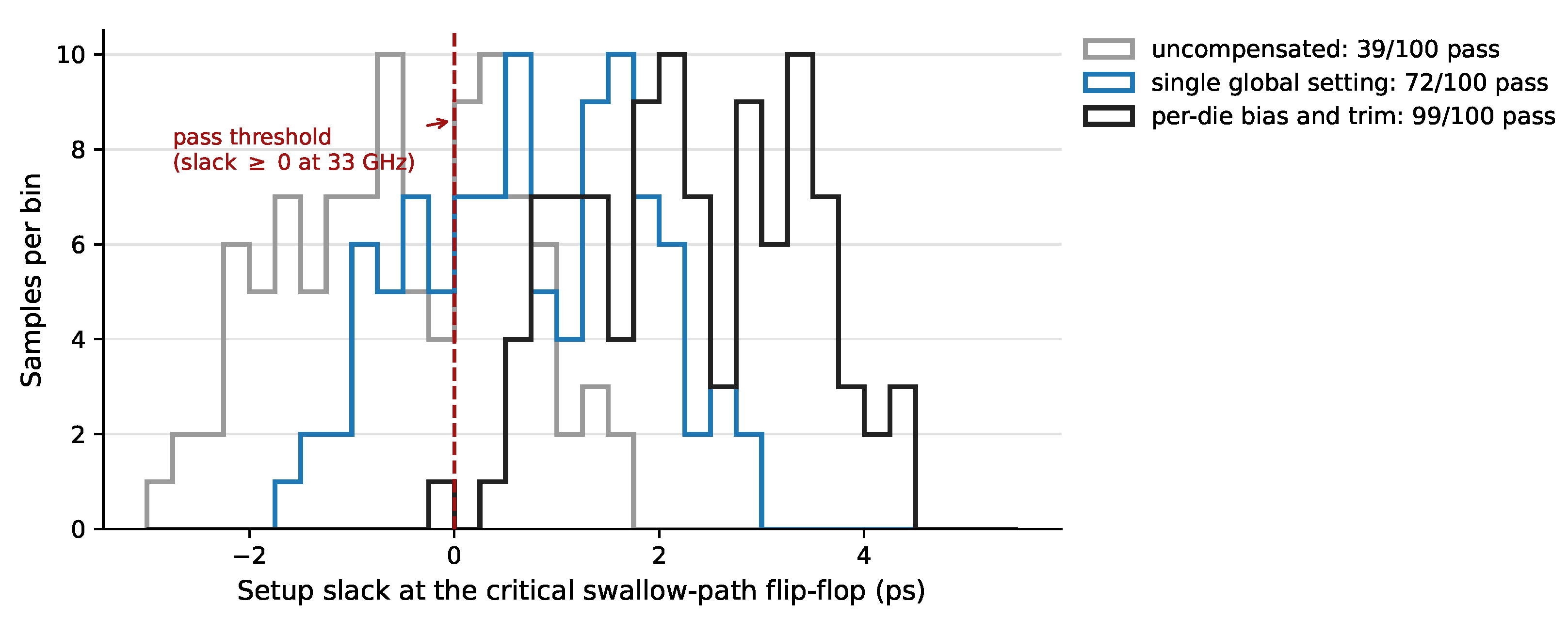
The campaign uses 100 samples and three compensation tiers, and the tiers are paired: each die is simulated three times, once uncompensated, once with a single global setting applied to every die, and once with a per-die bias and trim code. Pairing matters because the effect of a back-gate or trim setting is specific to the mismatch profile of the die it is applied to. Mismatch displaces the clock-tree insertion delay and the resolve time of the TSPC cells at the same time, so the improvement a given bias produces is not a fixed increment and cannot be inferred from the uncompensated result. The compensated tiers are therefore separately simulated rather than derived, giving 300 post-layout transient runs in total. In each run the setup slack is measured directly at the critical swallow-path flip-flop on the same system-level basis as in Section 3.6, that is, including the clock-tree insertion delay and the chain output edge rather than the local resolve margin of the front cell alone, and a sample passes when that slack is non-negative at the 33 GHz target.
Table 6 gives the resulting yields and Figure 13 the slack distributions. Uncompensated, 39 of 100 samples meet the target. A single global forward bias of 0.50 V with one shared trim code applied to every die raises this to 72 of 100, and a per-die bias and trim to 99 of 100. The intervals quoted with each yield are Wilson score intervals at 95 % confidence for the stated sample count; with 100 samples they span roughly ± 10 points at the middle tier, and the yields should be read with that width in mind rather than as point estimates.
The decomposition is informative about what each layer does. The global setting removes the common-mode part of the impairment: it lifts the whole distribution by a similar amount, and Figure 13 shows the uncompensated and global histograms as near-translations of one another. What it cannot remove is the die-to-die spread itself, and the residual failures at that tier are the samples whose mismatch places them far enough into the slow tail that a shared setting does not reach them. Allowing the bias and trim to be chosen per die narrows the distribution as well as shifting it, since each die receives the correction its own mismatch profile calls for, and the surviving failure is the single sample whose resolve-time deficit exceeds what the available bias range can recover.
Two limits on this result should be stated. First, the per-die tier is an upper bound rather than the yield of a self-contained system: every sample is individually optimized by the external search described below, which the proposed circuit does not implement, so the gain it shows over the global setting is available only at the cost of that per-die procedure. Second, the maximum frequency quoted per sample is not swept but converted from the measured slack at the operating point, f max = 1 / ( T 0 α Δ t ) with T 0 = 30.303 ps, since a nested frequency sweep over 300 runs would be prohibitive. The pass criterion depends only on the directly measured slack, so the yields do not rest on that conversion.
Three points of comparison with the corner results of Section 3.5 are worth making explicit since the two characterizations answer different questions. First, the maximum frequency quoted per Monte Carlo sample is the converted quantity just described and not the swept, transient-verified limit that Section 3.5 defines, so the two should not be compared sample by corner. Second, the mean of the Monte Carlo distribution lies below the nominal corner at the same supply and temperature, which is expected rather than anomalous: the maximum frequency of the chain is a minimum taken over its six stages, and adding mismatch to a minimum lowers its mean even when the underlying distributions are centred. Third, the global setting used here, a forward bias of 0.50 V, is larger than the per-corner values of Table 4 because it is chosen to maximize yield over the whole sampled population rather than to close one nominal corner; a single setting that must also reach the slow tail is necessarily more aggressive than the optimum for the corner alone.
A per-die setting requires a search procedure that the proposed circuit does not implement, and it is worth recording what that procedure is, since it bounds what per-die tuning could deliver. It is a monotone coarse-then-fine sweep over the trim codes and the two bias rails, using the divided output at N = 127 as the pass/fail observable, completing in about 20 at-speed iterations per die; the closed-loop controller noted in Section 2.5 would automate it. The choice of N = 127 as the observable follows from the modulus structure of Table 1: it is the ratio at which all six cells are active and none is forced transparent, so it exercises the longest modulus path the design contains. Because the per-stage timing error accumulates monotonically along the chain (Table 3), the accumulated error observed there is the largest the chain produces, and at smaller ratios the later cells are made transparent so that the active path is a strict subset of the calibrated one. A code set that passes at N = 127 therefore exercises every stage that any smaller ratio can exercise. This argument covers the accumulated swallow-path timing that the trim corrects; it does not extend to the low-frequency retention limit of Section 3.3, which depends on the input frequency rather than on the division ratio.

3.9. Power and Energy

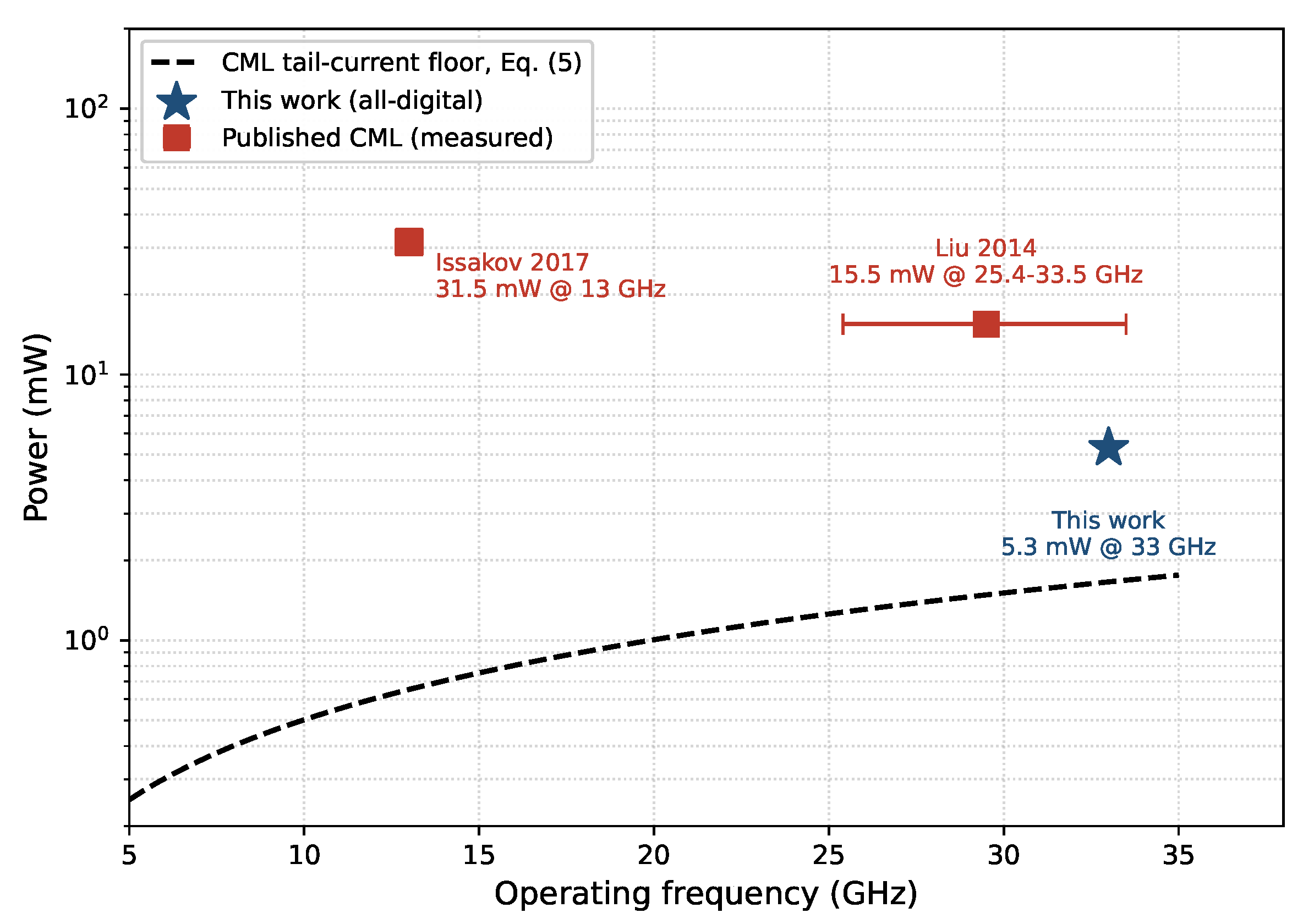
Power is the central quantitative result of this section. The all-digital divider was simulated at a 33 GHz input and 0.80 V supply; Table 7 reports its supply current and power. The current rises only weakly with N, from 4.8 mA at N = 8 to 6.6 mA at N = 127 , because the TSPC first stage toggles at the full input rate for all ratios while later stages add little. At the full ratio the divider consumes 5.3 mW at an energy of 0.16 pJ per input cycle, with the leakage component below 8 % at the typical corner, for a power-efficiency figure of merit of 6.2 GHz/mW. The reported power includes the per-stage trim cells, which sit in the signal path, and excludes the generation of the back-gate biases; automatic back-biasing units in FDSOI add about 2.5 μ W and 0.0067   mm 2 [22]. The power overhead is negligible, below 0.05 % of the divider budget, but the area is not: the cited regulator occupies about 1.3 × the area of the divider core itself, so a dedicated bias unit would more than double the block area. Such units are in practice shared across a chip rather than dedicated to a single block, and amortized over four or more blocks the area penalty falls below 35 % ; the comparison of Table 8 nevertheless reports the divider core alone, and the reader should read the area column with that boundary in mind. The monitors, adaptive controller, calibration state machine, and code storage that a self-contained implementation would additionally require are not designed here and are therefore not costed at all, which is a further reason the area and power figures of this work describe the divider rather than a complete compensation system. As established in Section 3.1, current-mode-logic dividers are bounded below by the frequency-proportional, always-on bias of Equation (5). The narrow-range, injection-locked CML divider of [5] consumes 15.5 mW at this speed, so the all-digital design is about 3 × more efficient at the same input frequency. This anchor is functionally different, a fixed narrow-range ILFD rather than a wide-range MMD, and lies two technology nodes away, so the ratio illustrates the activity-scaling advantage rather than a like-for-like comparison; the gap to the lower-frequency CML and BiCMOS designs of [3,4] is larger. This ratio spans two technology nodes (90 versus 22 nm), a supply difference ( 1.2 versus 0.80 V), and an evidence class (measured silicon versus post-layout simulation), so part of the gap reflects scaling rather than topology alone; the caveat is taken up in Section 4. The emphasis of this work, however, is not minimum power but robust operation at current-mode-logic speed with an activity-scaling, bias-free supply current. Figure 14 plots the power against both current-mode baselines.

3.10. Jitter and Phase Noise

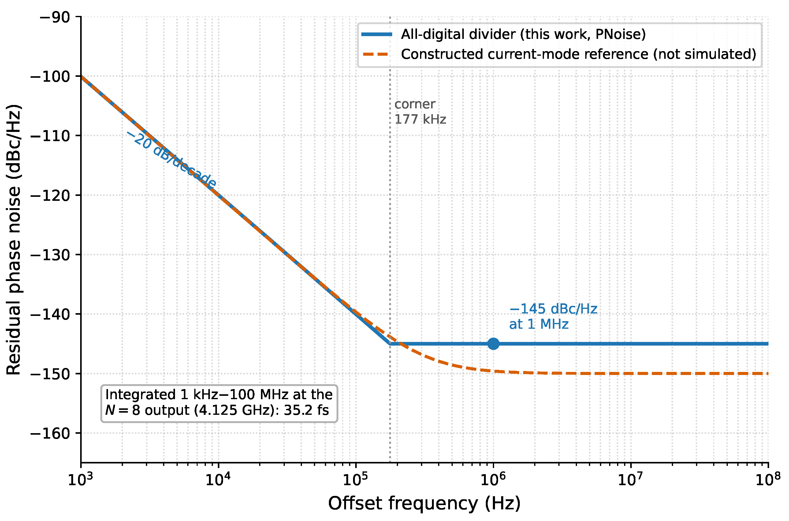
The additive jitter and residual phase noise were obtained from PSS and PNoise analysis. The periodic steady state of the divide-by-eight chain repeats at the output rather than at the input, so the PSS beat frequency is set to the 4.125 GHz output ( 242.42 ps) with eight harmonics retained to capture the 33 GHz input, and the PNoise analysis references the first harmonic, that is the output carrier, with maxsideband = 30 . Referred to that carrier the all-digital divider adds 35.2 fs RMS jitter (integrated from 1 kHz to 100 MHz) at N = 8 , with a phase-noise floor of 145 dBc/Hz reached beyond a corner at 177 kHz, below which the residual noise falls at 20 dB per decade from 100.1 dBc/Hz at 1 kHz. Of this total, the in-path delay-trim cells contribute about 3.1 fs, assessed by repeating the PNoise analysis at the minimum and maximum trim codes. The back gate also converts bias-rail ripple to threshold ripple through the sensitivity of Section 2.4; with a sensitivity of the setup margin at the critical flip-flop of about 1.5 ps per 100 mV of back-gate voltage, holding the back-gate rails below 2 mV of ripple keeps their contribution below 30 fs. This term is an externally injected disturbance rather than device noise, so it does not appear in the PNoise result and adds to it in quadrature, giving 46.2 fs in total. At the stated ripple bound the bias generator therefore contributes more jitter than the divider itself, which is what sets the filtering requirement on the shared bias rail. Current-mode dividers typically achieve somewhat lower additive jitter, of order tens of femtoseconds, as expected for a current-biased topology; this is a qualitative expectation drawn from published practice rather than a comparison performed here. The current-mode curve in Figure 15 is a constructed reference, not a design of this work and not a simulation result: it is drawn with the low-offset noise of the all-digital divider and an assumed flat floor of 150 dBc/Hz representative of published current-biased dividers. It is included only to indicate the direction and approximate scale of the expected difference, and no quantitative jitter comparison is drawn from it. Relative to a typical oscillator the all-digital additive jitter remains small, so the efficiency and speed advantages of the all-digital design are obtained at a modest noise penalty. In a closed loop the 35.2 fs additive jitter adds in quadrature to the much larger oscillator and charge-pump contributions and is therefore not expected to dominate the integrated jitter, although a full in-loop characterization is left to future work. Figure 15 shows the phase-noise curves.

3.11. Comparison with the State of the Art

Table 8 compares this work with recent programmable and multi-modulus dividers, separating current-mode and digital implementations. The closest prior art is the six-stage extended-range TSPC divider of [8], which shares the same 8 to 127 range. The present work differs in its 22 nm FDSOI implementation with back-gate compensation, its full post-layout corner characterization, and its combination of high speed with explicit PVT compensation, noting that the speed figures in the table are drawn from different nodes, supplies, and evidence classes and are therefore not directly rankable. Among the compared designs, this work is the only one to combine a wide 8 to 127 range, 39.5 GHz operation, and explicit PVT compensation while remaining compact at 0.005   mm 2 . It is the fastest entry in the table. The qualitative claim this work supports is architectural: an all-digital chain reaches this speed without an always-on bias current, so its supply current scales with activity. The quantitative comparison against the same-frequency narrow-range CML/ILFD divider of [5] should be read far more narrowly. The figure-of-merit ratio is 6.2 versus 2.2 GHz/mW, but the two entries differ in technology node (22 nm versus 90 nm), supply ( 0.80 V versus 1.2 V), functional class (wide-range multi-modulus versus narrow-range injection-locked), and evidence class (post-layout simulation versus silicon measurement). Supply scaling alone accounts for a factor of about ( 1.2 / 0.8 ) 2 2.3 in dynamic power, which is most of the observed ratio, so the residual attributable to topology is small and cannot be separated from the node difference with the data available. We therefore do not claim a threefold topological advantage; what the comparison establishes is that an all-digital divider operates in the same speed class as a current-mode design while drawing no static bias. The value of the present work is not the single lowest power but the unique combination of that speed with wide range, compactness, and PVT compensation, as the last column of Table 8 makes explicit. Some digital designs, the narrow-range TSPC divider of [16] and the wide-band E-TSPC divider of [32], report a higher raw power efficiency. Those numbers are nominal-corner results, however, and in the wide-range case a schematic-level one (Table 8), so they represent a best-case speed rather than an operating point guaranteed across process and temperature, and they are accompanied by neither a PVT-compensation mechanism nor corner and statistical characterization. The distinction is concrete: the uncompensated version of the present all-digital chain reaches a comparable nominal speed yet falls to 30.5 GHz at the slow-hot corner (Table 4), below the 33 GHz target, and it is precisely this corner that the compensation closes. Operation held across the full PVT box by a defined knob, rather than raw nominal efficiency, is the dimension this methodology targets. Two further qualifications belong with any comparison against current-mode logic. First, the CML entries of Table 8 are fixed-bias designs, whereas a CML divider can itself be optimized for the operating point: the tail current and the load resistance can be scaled together with the required speed so that a CML chain adapted to each stage’s frequency would consume considerably less than a chain biased uniformly for the front-stage rate. The comparison here is therefore against published practice, not against a CML divider optimized to the same degree as the present design, and the efficiency gap would narrow against such a reference. Second, the constant supply current of CML is not only a cost. Because it does not modulate with switching activity, it generates far less supply and substrate disturbance than a rail-to-rail chain, which is an advantage in electromagnetic emission and in coexistence with sensitive analog blocks on the same die; the activity-scaling current of the all-digital divider trades that quality for average power. Neither point is addressed by simulation in this work, and both should be weighed by a designer choosing between the two topologies. Measurement supports the second: in a 17 GHz TSPC multi-modulus divider embedded in a PLL, the single-ended logic was found to inject supply disturbance that coupled to the oscillator control voltage, giving a worst-case spur 58.9 dB below the carrier and requiring separate supply domains for the oscillator and the digital logic [14]. The same mechanism applies to the chain presented here.
The comparison of Table 8 lists uncompensated dividers, and it should be read alongside the other routes to PVT robustness rather than as the only one. Within the current-mode family the bias itself can be regulated: replica and feedback schemes that hold the load resistance and tail current of a CML latch against process and temperature have been demonstrated in divider chains, trading additional analog circuitry for a stabilized operating point. In the digital domain the supply is the alternative knob to the threshold, and adaptive voltage scaling closes the same corner spread by moving V D D rather than V t ; published comparisons report the two as complementary, with body bias offering a smaller tuning range at far lower energy cost and the two frequently combined [10,22]. The back gate is chosen here because it is available at no area cost in this technology, acts on the threshold directly, and can rebalance the NMOS and PMOS networks independently, which the supply cannot. No FDSOI multi-modulus divider reporting divider-level power and range figures was identified in the surveyed literature, so the table contains no FDSOI entry; the published FDSOI divider work addresses fixed-ratio prescalers and divider chains rather than wide-range programmable dividers, and the FDSOI precedents of Section 2.4 concern oscillators and mixed-signal blocks.

4. Discussion

The results support the central claim that the static current of a CML divider can be avoided without sacrificing the operating range or the target speed, provided the PVT sensitivity of the all-digital implementation is closed by design. The back gate proves to be an efficient global knob: over the range applied here a timing-margin recovery of approximately 1.5 ps per 100 mV of forward body bias is observed, which over the 0.28 V applied at the low-supply corners is sufficient to move the worst corner from a setup violation to a positive slack without supply scaling. This is consistent with the corner and temperature compensation reported for 22FDX digital and mixed-signal blocks [9,10,22].
The trim layers are deliberately bounded. As formalized in Section 2.5, the per-stage and integral-nonlinearity trims can only remove the error that lies in the span of the trim vectors, so a residual of 2.08 ps at the nominal corner, rising to 3.12 ps at the slow-hot corner, remains after trimming and is reported explicitly. This residual sets the floor on the achievable accuracy and is independent of how many trim codes are added, a point that is easy to overlook when a calibration is presented only by its code resolution.
The reported margins are time-zero quantities. Bias-temperature instability and hot-carrier injection shift the device thresholds over the product lifetime in the same direction as a slow process corner, so aging consumes setup margin exactly where it is scarcest. An assumed end-of-life threshold drift can be converted to an equivalent back-gate excursion through the coupling of Section 2.4, which is 70 to 85 mV of threshold shift per volt of back-gate bias. On that basis a drift of 20 to 30 mV corresponds to 0.24 to 0.43 V of back-gate equivalent, and therefore, at the observed 1.5 ps per 100 mV, to roughly 3.5 to 6.4 ps of lost setup margin. Set against the extracted post-layout setup slacks of Section 3.6, which span + 0.11 to + 2.40 ps across the corner box, this is not a fraction of the available margin but a multiple of it. The predicted drift exceeds the time-zero slack at every corner, by roughly 1.5 × at the most relaxed and by more than an order of magnitude at the tightest. A one-time bias and trim setting therefore cannot be expected to hold over life. The forward-bias reserve nevertheless retains the authority to recover it: restoring 6.4 ps requires about 0.43 V of additional forward bias, and since the applied front-stage bias reaches only 0.28 V the greater part of the usable window is still unused. Because bias-temperature instability acts principally on the PMOS devices while hot-carrier injection acts on the NMOS devices, aging also skews the relative edge rates and therefore reappears as the duty-cycle mechanism of Section 3.6, not only as a symmetric loss of setup margin. Lifetime tracking therefore requires periodic recalibration or the closed-loop controller noted in Section 2.5 rather than a one-time setting. The 20 to 30 mV drift used above is an assumed end-of-life range rather than a simulated result; transistor-level aging simulation would narrow it, and is left to future work. It would not alter the conclusion drawn here, which is that the degradation is of the order of the available setup margin rather than negligible against it, and that the back gate retains the authority to recover it.
Because no silicon is measured, the credibility of the work rests on the verification flow. Post-layout extraction captures the interconnect parasitics that dominate timing at this node, the corner box bounds the systematic component of the variation, and the paired Monte Carlo campaign of Section 3.8 quantifies the sensitivity to random variation that a corner sweep alone cannot capture. The same combination of corner sign-off and statistical analysis underlies the back-bias-aware industrial flows of [10,22], which lends external support to its use here as a measurement proxy. The methodology is not specific to this divider and can be applied to other all-digital blocks that must meet timing targets ordinarily served by current-mode logic.
Relative to the closest prior art, the six-stage extended-range TSPC divider of [8], the contribution is not the architecture, which is shared, but the implementation in 22 nm FDSOI with an explicit back-gate compensation method, the post-layout corner characterization, and the efficiency advantage over the same-frequency current-mode-logic divider. Four limitations remain. First, the comparison with current-mode logic rests on published designs in older nodes and on the analytical bound of Equation (5); no same-node CML reference cell was designed, so the efficiency figure should be read against published practice rather than against an optimized 22 nm CML implementation. In particular, the divider of [5] is an injection-locked, narrow-range design measured in 90 nm silicon at 1.2 V, so the 3 × ratio mixes topology with node and supply scaling; the qualitative claim, the absence of an always-on bias, is unaffected, but the numeric ratio should not be read as a same-node topology comparison. Second, the generation of the back-gate biases is not designed in this work; its overhead is estimated from published FDSOI back-biasing regulators [22,23], and the bias and trim settings are applied as one-time per-corner or per-die values rather than by the closed-loop controller noted in Section 2.5. Third, the Monte Carlo campaign uses 100 samples at a single corner, so the reported yields carry confidence intervals of roughly ten points and do not resolve the supply and temperature dependence of the yield itself. Fourth, no silicon is measured; fabrication and measurement of the divider, including its behavior inside a closed PLL, are the subject of future work.

5. Conclusions

An all-digital multi-modulus divider in 22 nm FDSOI has been presented together with the design and verification methodology that closes the PVT sensitivity of a timing-sensitive all-digital implementation in post-layout simulation. The results establish post-layout feasibility at the 33 GHz target rather than a demonstrated replacement for current-mode hardware: no same-node CML reference cell was designed and no silicon has been measured. By removing the constant bias current of CML and balancing speed against power with digital cells, the divider consumes 5.3 mW at N = 127 with an activity-scaling, bias-free supply current, while covering N = 8 to 127 at up to 39.5 GHz in a compact 0.005   mm 2 core. The three-method compensation scheme, built on the FDSOI back gate, per-stage delay trim, and a bounded integral-nonlinearity trim, closes the setup, hold, and duty-cycle failure modes, and the design achieves a worst-case post-layout maximum frequency of 33.0 GHz across the PVT box, at the cold low-supply corner, against the 33 GHz target. Across 100 Monte Carlo samples at that corner the yield rises from 39% uncompensated to 72% with a single global back-gate setting and 99% with a per-die setting. These settings are selected externally and applied as one-time per-corner or per-die values; taken together with the lifetime threshold drift analyzed in Section 4, which exceeds the post-compensation setup margin at every corner, this makes the closed-loop controller of Section 2.5 a requirement for a deployable implementation rather than a refinement of one. Future work will design that control loop, validate the methodology in silicon, and characterize the divider inside a closed PLL.

Author Contributions

Conceptualization, S.K. and D.C.; methodology, S.K.; software, S.K.; validation, S.K., E.N.D. and B.A.; formal analysis, S.K.; investigation, S.K., E.N.D. and R.K.S.; writing—original draft preparation, S.K.; writing—review and editing, E.N.D., B.A., R.K.S. and D.C.; visualization, S.K.; supervision, D.C.; project administration, D.C. All authors have read and agreed to the published version of the manuscript.

Funding

This research received no external funding.

Institutional Review Board Statement

Not applicable.

Informed Consent Statement

Not applicable.

Data Availability Statement

The simulation data supporting the reported results are available from the corresponding author upon reasonable request. Foundry-related design data are subject to a non-disclosure agreement and cannot be shared.

Acknowledgments

The authors used Anthropic’s Claude (Sonnet 5) during the preparation and revision of this manuscript. It was used for (i) language editing, including a full clarity, grammar, and consistency pass over the revised text; (ii) assistance in locating relevant references; and (iii) suggesting supplementary supporting evidence and related work. All circuit design, simulation, and parasitic extraction were performed by the authors, and every figure reports data the authors generated. The core research ideas, circuit analyses, and derivations are the authors’ original work.

Conflicts of Interest

The authors declare no conflicts of interest.

Abbreviations

The following abbreviations are used in this manuscript:
BBBody Bias (externally applied)INLIntegral Nonlinearity
CMLCurrent-Mode LogicLVSLayout Versus Schematic
DFFD Flip-FlopLVTLow Threshold Voltage
DRCDesign-Rule CheckMMDMulti-Modulus Divider
E-TSPCExtended True Single-Phase ClockPLLPhase-Locked Loop
FBBForward Body BiasPVTProcess, Voltage, Temperature
FDSOIFully Depleted Silicon-On-InsulatorRBBReverse Body Bias
HVTHigh Threshold VoltageRVTRegular Threshold Voltage
ILFDInjection-Locked Frequency DividerTSPCTrue Single-Phase Clock

References

  1. Vaucher, C.S.; Ferencic, I.; Locher, M.; Sedvallson, S.; Voegeli, U.; Wang, Z. A family of low-power truly modular programmable dividers in standard 0.35-μm CMOS technology. IEEE J. Solid-State Circuits 2000, 35, 1039–1045. [Google Scholar] [CrossRef] [Scilit]
  2. Wang, Y.; Wang, Y.; Wu, Z.; Quan, Z.; Liou, J.J. A Programmable Frequency Divider with a Full Modulus Range and 50% Output Duty Cycle. IEEE Access 2020, 8, 102032–102039. [Google Scholar] [CrossRef] [Scilit]
  3. Issakov, V.; Trotta, S. Low-power dual-modulus frequency divider by 4/5 up to 13-GHz in 0.13 μm CMOS. In Proceedings of the 2017 IEEE International Conference on Microwaves, Antennas, Communications and Electronic Systems (COMCAS), Tel-Aviv, Israel, 13–15 November 2017. [Google Scholar]
  4. Cheng, G.; Li, Z.; Wu, W. Analysis and design of low power wideband programmable frequency divider in 0.13-μm SiGe BiCMOS technology. AEU Int. J. Electron. Commun. 2021, 138, 153879. [Google Scholar] [CrossRef] [Scilit]
  5. Liu, F.; Wang, Z.; Li, Z.; Li, Q.; Yang, G.; Guo, T. Low-power 25.4–33.5 GHz programmable multi-modulus frequency divider. Electron. Lett. 2014, 50, 1067–1068. [Google Scholar] [CrossRef] [Scilit]
  6. Chen, Z.; Zhang, Y.; Tang, X.; Li, J.; Huang, F.; Jiang, N. Design of Low Power Consumption, High-Speed and Wide Division Ratio Range Programmable Frequency Divider. In Proceedings of the 2020 IEEE 5th International Conference on Integrated Circuits and Microsystems (ICICM), Nanjing, China, 23–25 October 2020. [Google Scholar]
  7. Lin, C.S.; Chien, T.H.; Wey, C.L. A 5.5-GHz 1-mW Full-Modulus-Range Programmable Frequency Divider in 90-nm CMOS Process. IEEE Trans. Circuits Syst. II Express Briefs 2011, 58, 550–554. [Google Scholar] [CrossRef] [Scilit]
  8. Kulkarni, P.; Garg, S.; Agrawal, S.; Shojaei Baghini, M. Low Power Extended Range Multi-Modulus Divider Using True-Single-Phase-Clock Logic. In Proceedings of the 2021 34th International Conference on VLSI Design and 2021 20th International Conference on Embedded Systems (VLSID), Guwahati, India, 20–24 February 2021. [Google Scholar]
  9. Wittenhagen, E.; Runge, M.; Lotfi, N.; Ghafarian, H.; Tian, Y.; Gerfers, F. Advanced Mixed Signal Concepts Exploiting the Strong Body-Bias Effect in CMOS 22FDX. IEEE Trans. Circuits Syst. Regul. Pap. 2021, 68, 57–66. [Google Scholar] [CrossRef] [Scilit]
  10. Höppner, S.; Eisenreich, H.; Walter, D.; Scharfe, A.; Oefelein, A.; Schraut, F.; Prengel, H. Adaptive Body Bias Aware Implementation for Ultra-Low-Voltage Designs in 22FDX Technology. IEEE Trans. Circuits Syst. II Express Briefs 2020, 67, 2159–2163. [Google Scholar] [CrossRef] [Scilit]
  11. Gerfers, F.; Lotfi, N.; Wittenhagen, E.; Ghafarian, H.; Tian, Y.; Runge, M. Body-Bias Techniques in CMOS 22FDX for Mixed-Signal Circuits and Systems. In Proceedings of the 2019 26th IEEE International Conference on Electronics, Circuits and Systems (ICECS), Genoa, Italy, 27–29 November 2019. [Google Scholar]
  12. Tibenszky, Z.; Carta, C.; Ellinger, F. A 0.35 mW 70 GHz Divide-by-4 TSPC Frequency Divider on 22 nm FD-SOI CMOS Technology. In Proceedings of the 2020 IEEE Radio Frequency Integrated Circuits Symposium (RFIC), Los Angeles, CA, USA, 4–6 August 2020; pp. 243–246. [Google Scholar]
  13. Tibenszky, Z.; Kreißig, M.; Carta, C.; Ellinger, F. A 0.35-mW 70-GHz Self-Resonant E-TSPC Frequency Divider with Backgate Adjustment. IEEE Trans. Microw. Theory Tech. 2022, 70, 2236–2247. [Google Scholar] [CrossRef] [Scilit]
  14. Krishna, M.V.; Jain, A.; Quadir, N.A.; Townsend, P.D.; Ossieur, P. A 1V 2mW 17GHz Multi-Modulus Frequency Divider based on TSPC Logic using 65nm CMOS. In Proceedings of the ESSCIRC 2014—40th European Solid State Circuits Conference (ESSCIRC), Venice Lido, Italy, 22–26 September 2014; pp. 431–434. [Google Scholar]
  15. Zhao, M.; Huang, J. Design of a multi-modulus divider with a wide frequency dividing range and low power consumption. J. Phys. Conf. Ser. 2023, 2524, 012008. [Google Scholar] [CrossRef] [Scilit]
  16. Shao, Y.; Liu, H.; Wang, W. A High-Speed Low Power Multi-Modulus Frequency Divider based on TSPC logic using 55 nm CMOS. IOP Conf. Ser. Mater. Sci. Eng. 2018, 452, 042120. [Google Scholar] [CrossRef] [Scilit]
  17. Krishna, M.V.; Do, M.A.; Yeo, K.S.; Boon, C.C.; Lim, W.M. Design and Analysis of Ultra Low Power True Single Phase Clock CMOS 2/3 Prescaler. IEEE Trans. Circuits Syst. Regul. Pap. 2010, 57, 72–82. [Google Scholar] [CrossRef] [Scilit]
  18. Radhapuram, S.; Bae, J.; Jo, I.; Kihara, T.; Matsuoka, T. A low-power CMOS programmable frequency divider with novel retiming scheme. IEICE Electron. Express 2015, 12, 20141233. [Google Scholar] [CrossRef] [Scilit][Green Version]
  19. Ong, S.N.; Chan, L.H.K.; Chew, K.W.J.; Lim, C.K.; Oo, W.L.; Bellaouar, A.; Zhang, C.; Chow, W.H.; Chen, T.; Rassel, R.; et al. 22 nm FD-SOI Technology with Back-biasing Capability Offers Excellent Performance for Enabling Efficient, Ultra-low Power Analog and RF/Millimeter-Wave Designs. In Proceedings of the 2019 IEEE Radio Frequency Integrated Circuits Symposium (RFIC), Boston, MA, USA, 2–4 June 2019. [Google Scholar]
  20. Blackwell, D.; Hui, X.; Wang, Y.; Duan, H.; Hang, P.; Ton-That, V.; Ginawi, A.; Wehbi, A. Novel Analog Designs with Back-Gate Bias by Using Global Foundries 22FDX Technology. In Proceedings of the 2022 IEEE 5th International Conference on Electronics Technology (ICET), Chengdu, China, 13–16 May 2022. [Google Scholar]
  21. Arnaud, F.; Clerc, S.; Haendler, S.; Bingert, R.; Flatresse, P.; Huard, V.; Poiroux, T. Enhanced design performance thanks to adaptative body biasing technique in FDSOI technologies. In Proceedings of the 2017 IEEE SOI-3D-Subthreshold Microelectronics Technology Unified Conference (S3S), Burlingame, CA, USA, 16–19 October 2017. [Google Scholar]
  22. Quelen, A.; Pillonnet, G.; Flatresse, P.; Beigne, E. A 2.5 μW 0.0067 mm2 automatic back-biasing compensation unit achieving 50% leakage reduction in FDSOI 28 nm. In Proceedings of the 2018 IEEE International Solid-State Circuits Conference—(ISSCC), San Francisco, CA, USA, 11–15 February 2018. [Google Scholar]
  23. Moursy, Y.; Raupp da Rosa, T.; Jure, L.; Quelen, A.; Genevey, S.; Pierrefeu, L.; Grand, E.; Winkler, J.; Park, J.; Pillonnet, G.; et al. A 0.021 mm2 PVT-Aware Digital-Flow-Compatible Adaptive Back-Biasing Regulator with Scalable Drivers Achieving 450% Frequency Boosting and 30% Power Reduction in 22 nm FDSOI Technology. In Proceedings of the 2021 IEEE International Solid-State Circuits Conference (ISSCC), San Francisco, CA, USA, 13–22 February 2021; pp. 492–494. [Google Scholar]
  24. Pazionis, P.; Tsimpos, A.; Theodoratos, G.; Panagopoulos, G. A 4.8ps Resolution, PVT-insensitive Vernier-based TDC using switched-RO PLL and Back Gate Calibration. In Proceedings of the 2025 IEEE Computer Society Annual Symposium on VLSI (ISVLSI), Kalamata, Greece, 6–9 July 2025. [Google Scholar]
  25. Sathanur, A.; Pullini, A.; Benini, L.; De Micheli, G.; Macii, E. Physically clustered forward body biasing for variability compensation in nanometer CMOS design. In Proceedings of the 2009 Design, Automation & Test in Europe Conference & Exhibition, Nice, France, 20–24 April 2009. [Google Scholar]
  26. Ma, S.; Mo, T.; Wang, H.; Chen, Z.; Kang, Z.; Hu, K. A Wide-Range Oscillator with Dual-Mode Calibration and Duty Cycle Control. In Proceedings of the 2025 7th International Conference on Electronic Engineering and Informatics (EEI), Yangzhou, China, 7–9 November 2025. [Google Scholar]
  27. Yang, Y.; Deng, W.; Yan, A.; Jia, H.; Gong, J.; Wang, Z.; Chi, B. A Low-Spur and Low-Jitter Fractional Output Divider with Self-Adaption Frequency Filtering Technique. IEEE J. Solid-State Circuits 2025, 60, 4167–4179. [Google Scholar] [CrossRef] [Scilit]
  28. Eissa, A.I.; Alvarez-Fontecilla, E.; Weltin-Wu, C.; Galton, I. A Duty-Cycle-Error-Immune Reference Frequency Doubling Technique for Fractional-N Digital PLLs. IEEE Trans. Circuits Syst. Regul. Pap. 2024, 71, 4524–4537. [Google Scholar] [CrossRef] [Scilit]
  29. Kao, S.K.; Liu, S.I. All-Digital Fast-Locked Synchronous Duty-Cycle Corrector. IEEE Trans. Circuits Syst. II Express Briefs 2006, 53, 1363–1367. [Google Scholar] [CrossRef] [Scilit]
  30. Hai, Y.; Liu, F.; Wang, Y. A wide-frequency all-digital duty cycle corrector with self-adaptive configurable delay chain. IEICE Electron. Express 2024, 21, 20230557. [Google Scholar] [CrossRef] [Scilit]
  31. Li, Z.; Deng, L.; Li, C.; Yan, C.; Qian, Z.; Shan, W. A 250M-2.5GHz Two-Stage Duty-Cycle Corrector with 10%–90% Correction Range and 3-Cycle Correction Latency for Mitigating Aging Effects. In Proceedings of the 2025 IEEE International Symposium on Circuits and Systems (ISCAS), London, UK, 25–28 May 2025. [Google Scholar]
  32. Chen, P.L.; Tsai, M.L.; Sheu, M.H. VLSI Design for Low-power and Wide-band Programmable Frequency Divider. In Proceedings of the 2023 IEEE 5th Eurasia Conference on IOT, Communication and Engineering (ECICE), Yunlin, Taiwan, 27–29 October 2023. [Google Scholar]
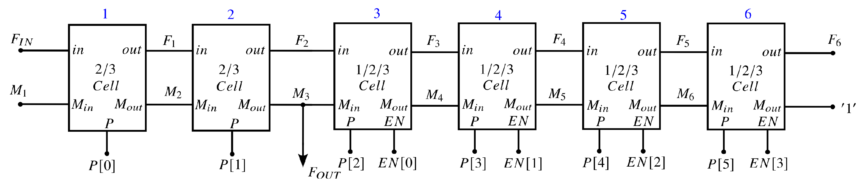
Figure 1. Architecture of the all-digital multi-modulus divider. The input F IN is processed by a cascade of six programmable divider cells: the first two high-speed stages are 2/3 cells and the remaining four are extended-range 1/2/3 cells. Each cell divides under the control of a program bit P [ i ] and exchanges a modulus-request signal ( M in , M out ) with its neighbor, while the enable inputs E N of the later stages force a stage transparent to reach the low end of the range. The output F OUT is taken from the modulus terminal of the last active stage.
Electronics 15 04036 g001
Figure 5. The delay-trim unit cell of Method 2. (a) Digitally controlled shunt-capacitor delay element. The inter-stage path is driven at full strength, and switched capacitor branches on the internal node set the delay: the fine branches carry unit capacitors C u gated by the fine code bits b f , and the coarse branches binary-weighted multiples of C u gated by the coarse code bits b c so that the coarse and fine codes span the range and the resolution respectively. Branch counts are drawn representatively; the code width is B as introduced in Section 2.5. The switch devices are the 0.10 μ m/20 nm RVT devices of Section 2.5; their back gate is not connected to any of the four rails of Table 2 but held at a fixed potential, which is what keeps Methods 1 and 2 independent. (b) Placement in the chain. The trim cells, marked T, sit in the inter-stage paths feeding the timing-critical stages 1–3, and the divided-down back-end stages 4–6 carry none. Because the output of stage k clocks stage k + 1 , a single code step displaces the modulus window of the trimmed stage and of every stage downstream of it by the same amount, which is the coupling that makes the correction vectors { δ k } of Section 2.5 reach beyond the trimmed stages.
Electronics 15 04036 g005
Figure 6. Error-span limit of the systematic trim (Method 3), for the post-layout error vector of Table 3. The delay trim cancels the errors of the timing-critical front stages (1–3) and, through the inter-stage path, the common-mode component of the untrimmed back-end stages (4–6); their relative spread lies outside span { δ k } and sets the out-of-span residual floor, about 2.08 ps at the nominal corner. The floor is a property of the uncorrected error subspace, not of the trim code resolution.
Electronics 15 04036 g006
Figure 7. Power versus operating frequency for current-mode logic and this work. The dashed line is the analytical CML tail-current floor of Equation (5), drawn for C L = 10 fF, Δ V = 250 mV, and four high-speed latches at 0.8 V; as a bound on the bias term alone it lies below the realized power of every plotted design, including this work, and is shown to convey the continuous, frequency-proportional nature of the CML supply current rather than a power magnitude. The squares are the measured power of published CML dividers, 31.5 mW at 13 GHz [3] (including a 50 Ω measurement buffer) and 15.5 mW over 25.4 33.5 GHz [5]; the star is the all-digital design of this work, about 3 × below the same-frequency narrow-range CML/ILFD divider of [5]. Values are reported at each design’s own supply and node.
Electronics 15 04036 g007
Figure 8. Post-layout view of the divider core in 22 nm FDSOI, occupying 100 × 50 μ m2 ( 0.005   mm 2 ), shown without I/O pins.
Electronics 15 04036 g008
Figure 9. Post-layout transient waveforms of the divider at a 33 GHz input clock, typical corner, for N = 8 , 31 , 64 , 127 , producing output frequencies of 4.13 GHz, 1.06 GHz, 516 MHz, and 260 MHz. The period of each output is marked. The input clock is drawn in blue, and the divided outputs for N = 8 , 31, 64 and 127 in orange, yellow, purple and green, respectively.
Electronics 15 04036 g009
Figure 10. Input sensitivity of the TSPC front stage: minimum input amplitude for correct division versus input frequency, at the typical corner (solid) and the slow-hot corner with body bias (dashed). The 33 GHz operating points (151 and 241 mV) and the 41 GHz maximum toggle frequency are marked.
Electronics 15 04036 g010
Figure 11. The three PVT failure modes after closure by Method 1, across the full corner box (post-layout, 33 GHz, N = 127 ). Each marker is one of the 45 simulated operating points of Table 4; marker shape denotes the supply and fill denotes the temperature. (a) Setup slack at the critical swallow-path flip-flop, positive at every point, with the binding value of + 0.11 ps at the cold low-supply corner. (b) Hold slack, positive at every point; the fast-cold corner, where the constraint binds, is held by the reverse bias applied to the back-stage rails. (c) Internal clock duty cycle of the TSPC front cell, held within 49.8 to 58.0 % once the wells are independently biased, against the 62 / 38 % collapse that occurs at the skewed corners without it.
Electronics 15 04036 g011
Figure 12. The duty-cycle mechanism at the skewed corner (SF, 0.72 V, 125   ° C), drawn as a constructed illustration rather than as extracted data. The binding, short evaluate phase of the TSPC front cell is plotted against front-cell frequency for the uncompensated 62 / 38 % duty and for the rebalanced duty obtained with independent well biasing, each against its front-cell resolve time τ res . Uncompensated, the short phase meets τ res at 32.2 GHz, below the 33 GHz target, so the front cell drops cycles; the forward bias that accompanies the rebalancing also lowers τ res , moving the crossing above the target and restoring operation. The curves are analytic and the resolve-time and edge-skew magnitudes are representative values chosen to be consistent with the simulated duty; the figure is included to show the mechanism, and the compensated duty values actually extracted at this corner are those of Table 4.
Electronics 15 04036 g012
Figure 13. Monte Carlo distribution of the setup slack at the critical swallow-path flip-flop, 100 paired samples with process and mismatch variation at 0.72 V and 40   ° C. The dashed line is the pass criterion, a non-negative slack at the 33 GHz target. The global setting translates the distribution without appreciably narrowing it, which is the signature of a common-mode correction; the per-die setting both shifts and narrows it, since each die receives the correction its own mismatch calls for.
Electronics 15 04036 g013
Figure 14. Power versus division ratio at a 33 GHz input and 0.80 V, typical corner (Table 7), against two current-mode references of Section 3.1: the measured same-frequency CML/ILFD divider of [5] (90 nm, reported at its own 1.2 V supply and node), which anchors the magnitude comparison, and the conservative analytical CML bias floor of Equation (5), a lower bound on the bias term shown for mechanism only and lying below the realized power of both designs. The all-digital power scales with activity and lies about 3 × below the measured reference at N = 127 . That ratio is a raw power comparison between designs at different nodes, supplies, and evidence classes, of which supply scaling alone accounts for roughly ( 1.2 / 0.8 ) 2 ; it is not a topological advantage, and the annotation is scoped accordingly.
Electronics 15 04036 g014
Figure 15. Residual phase noise of the all-digital divider from the PSS/PNoise sweep at the N = 8 output ( 4.125 GHz) with a 33 GHz input, shown together with a constructed current-mode reference (assumed flat 150 dBc/Hz floor). The reference is not a design of this work and is not a simulation result; it is drawn only as a qualitative illustration of the expected direction of the difference and should not be read as a quantitative comparison.
Electronics 15 04036 g015
Table 1. Contiguous division bands of the six-stage divider. Holding 6 m of the later cells transparent leaves m active 2 / 3 stages; the four bands tile the full N = 8 to 127 range without a gap. The four ratios N = 8 , 31 , 64 , 127 used as representative operating points fall in three of the bands; the 32–63 band is reached by the same mechanism but is not among the four spot-verified ratios.
Active Stages mTransparent CellsDivision Band NRepresentative N
338–158
4216–3131
5132–63
6064–12764, 127
Table 2. Back-gate rail assignment. The back-gate terminal of every device in Figure 2 and Figure 3 is drawn explicitly and labelled with its cell-level pin, V BG , N for the NMOS and V BG , P for the PMOS. Which well that pin biases, and which rail drives it, is set by the well configuration of the stage in which the cell is instantiated, so the two assignments are exchanged between the front and the later stages. The wells are those of the cross-sections in Figure 4a and the bias magnitudes those of Section 2.5.
Stage GroupWell Config./Vt FlavorVBG,N (NMOS Back Gate)VBG,P (PMOS Back Gate)
Stages 1–2 (2/3 cells)flipped/LVTdeep n-well, V DNW , F p-well, V PW , F
Stages 3–6 (1/2/3 cells)conventional/RVT–HVTp-well, V PW , B deep n-well, V DNW , B
Delay-trim cells (Method 2)conventional/RVTfixed, not drivenfixed, not driven
Table 3. Post-layout per-stage swallow-path timing error, extracted from transient simulation at the 33 GHz target, referenced to the clock edge at the critical flip-flop. Only the timing-critical stages 1–3 carry the delay trim; because the trim cells sit in the inter-stage path, a code step also displaces every stage downstream, so the back-end common-mode error is corrected and only its spread survives.
Stageei, TT (ps)ei, SS/0.72 V/125 °C (ps)Delay Trim
1 (2/3 cell, TSPC) 0.171 0.401 yes
2 (2/3 cell) 0.702 1.162 yes
3 (1/2/3 cell) 1.433 2.133 yes
4 (1/2/3 cell) 2.264 3.314 no
5 (1/2/3 cell) 3.195 4.705 no
6 (1/2/3 cell) 4.226 6.306 no
e res after trim 2.08 3.12
Table 4. Post-layout PVT matrix: maximum operating frequency without and with the applied back-gate bias, with the applied rail voltages and trim code, at N = 127 and the f max criterion of Section 3.5. V BG , F is the front-stage rail pair and V BG , B the back-stage pair, each quoted as the well potential referred to the supply rail of the corresponding polarity; the two columns of a pair are the n-side and p-side wells, which are driven independently. Slacks are the extracted system-level values at the critical swallow-path flip-flop. All 45 points meet the 33 GHz target. The composite trim code is the six-bit word applied to the delay-trim cells of Section 2.5: a three-bit coarse field in bits [ 5 : 3 ] and a three-bit fine field in bits [ 2 : 0 ] , gating respectively the binary-weighted and the unit shunt-capacitor branches of Figure 5a, with 0 x 00 applying no added capacitance. The values are absolute settings, one coarse step corresponding to 1.05 ps and one fine step to 0.13 ps of applied delay; in these corner runs a single shared word is applied to all three trimmed stages.
Cor.VDDTVBG,F (V)VBG,B (V)Comp.fmaxfmaxSetup
(V)(°C)npnpCodeno BBBB(ps)
SS0.72−40+0.28−0.280x1F29.833.20.11
SS0.7227+0.28−0.280x1A30.033.80.14
SS0.72125+0.28−0.280x1F30.535.02.10
SS0.80−40+0.15−0.150x1236.040.50.85
SS0.8027+0.15−0.150x1237.041.51.05
SS0.80125+0.15−0.150x1436.841.00.95
SS0.88−400x0843.543.51.20
SS0.88270x0842.542.51.10
SS0.881250x0841.041.00.95
TT0.72−400x0834.534.50.65
TT0.72270x0835.035.00.70
TT0.721250x0835.235.20.72
TT0.80−400x0A40.240.21.50
TT0.80270x0A39.539.51.40
TT0.801250x0A38.838.81.25
TT0.88−400x0A48.548.52.10
TT0.88270x0A47.047.01.95
TT0.881250x0A45.045.01.75
SF0.72−40+0.18−0.120x1431.033.50.35
SF0.7227+0.18−0.120x1431.534.00.38
SF0.72125+0.18−0.120x1432.034.50.42
SF0.80−40+0.18−0.120x1136.237.50.90
SF0.8027+0.18−0.120x1136.538.00.95
SF0.80125+0.18−0.120x1135.537.00.85
SF0.88−400x0A44.044.01.60
SF0.88270x0A43.043.01.50
SF0.881250x0A41.541.51.35
FS0.72−40+0.12−0.180x1430.533.00.30
FS0.7227+0.12−0.180x1431.033.50.32
FS0.72125+0.12−0.180x1431.534.00.35
FS0.80−40+0.12−0.180x1335.537.00.85
FS0.8027+0.12−0.180x1335.537.50.88
FS0.80125+0.12−0.180x1334.536.50.80
FS0.88−400x0A43.043.01.55
FS0.88270x0A42.042.01.45
FS0.881250x0A40.540.51.30
FF0.72−40+0.50−0.500x2A45.044.01.70
FF0.7227+0.50−0.500x2A44.043.01.60
FF0.72125+0.50−0.500x2A42.541.51.45
FF0.80−40+0.50−0.500x2A54.052.02.40
FF0.8027+0.50−0.500x2A52.050.02.25
FF0.80125+0.50−0.500x2A50.048.02.05
FF0.88−40+0.50−0.500x2A61.046.51.80
FF0.8827+0.50−0.500x2A59.045.01.65
FF0.88125+0.50−0.500x2A57.044.01.50
Table 5. The three PVT failure modes and their closure. The compensated slacks are the extracted post-layout system-level values at the critical swallow-path flip-flop, which include the clock-tree insertion delay and the chain output edge; they are therefore tighter than a local front-cell resolve margin measured at the same corner. The uncompensated setup and hold entries are reported as the functional outcome rather than as a slack, since the uncompensated slack was not extracted.
ModeCornerBeforeAfter (Method)
Setup slackSS, 0.72 V, 125 °Cfails ( f max = 30.5  GHz) + 2.10  ps (M1 FBB)
Hold slackFF, 0.88 V, −40 °Cfails (back-stage race) + 1.05  ps (M1 RBB)
Duty cycleSF, 0.72 V, 125 °C62/38% (fails)50.5/49.5% (M1 well rebalance)
Table 6. Monte Carlo yield at the 33 GHz target, 0.72 V and 40   ° C, from 100 paired samples with process and mismatch variation. A sample passes when the measured setup slack at the critical swallow-path flip-flop is non-negative. Intervals are Wilson score intervals at 95 % confidence. The per-die tier is the yield after idealized per-die calibration, in which every sample is individually optimized by an external search that the proposed circuit does not implement.
CompensationSettingYield (of 100)95% CI
None39.0% (39)30.0–48.8%
Single globalFBB 0.50  V, shared trim72.0% (72)62.5–79.9%
Per-die bias + trimper-die code, idealized99.0% (99)94.6–99.8%
Table 7. Supply current and power of the all-digital divider at a 33 GHz input, 0.80 V, typical corner.
Nfout (MHz)Supply Current (mA)Power (mW)
841254.83.8
3110655.64.5
645166.14.9
1272606.65.3
Table 8. Comparison with the state of the art for programmable and multi-modulus dividers. The entries differ in technology node, supply, functional class, and evidence class, so the table supports architectural comparison rather than like-for-like quantitative ranking; the evidence class of every row is marked, and the caveats are discussed in the text.
ReferenceTech.LogicRange (N) V DD (V) f max (GHz)Power (mW)FoM aArea ( mm 2 )PVT Comp.
[7M90 nmStatic1–2561.05.51.05.50.0011No
[3M0.13  μ mCML4/51.51331.50.410.009No
[5M90 nmCML/ILFD542–6541.233.515.52.20.34No
[16M55 nmTSPC32–691.2150.17880.0007No
[2M0.18  μ mStatic1–2561.82.33.40.68No
[6S0.18  μ mTSPC16–1591.84.710.60.44No
[8S65 nmTSPC8–1270.956.01.63.75No
[14M65 nmTSPC64–140 b1.0172.08.50.00125No
[32S40 nmE-TSPC16–2630.9300.3294No
This work PL22 nm FDSOITSPC+stat.8–1270.8039.55.36.20.005Yes
a FoM = frequency/power; for the cited designs the maximum frequency and its published power are used, and for this work the 33 GHz operating point (the value is frequency-independent for this design, whose power scales with frequency). M measured, S schematic simulation, PL post-layout simulation. b seven non-contiguous ratios (64, 80, 96, 100, 112, 120, 140) rather than a contiguous range. This work is the only entry with explicit PVT compensation (externally applied back-gate body bias plus trim).
Disclaimer/Publisher’s Note: The statements, opinions and data contained in all publications are solely those of the individual author(s) and contributor(s) and not of MDPI and/or the editor(s). MDPI and/or the editor(s) disclaim responsibility for any injury to people or property resulting from any ideas, methods, instructions or products referred to in the content.