
Article

Joint Multiplier–Adder Approximation with Flag-Based Error Recovery for BF16 Digital Compute-in-Memory

Department of Electronic Engineering, Seoul National University of Science and Technology, Seoul 01811, Republic of Korea
*
Author to whom correspondence should be addressed.
Electronics 2026, 15(17), 3861; https://doi.org/10.3390/electronics15173861
Submission received: 4 August 2026 / Revised: 21 August 2026 / Accepted: 26 August 2026 / Published: 27 August 2026
(This article belongs to the Special Issue Emerging Computing Paradigms for Efficient Edge AI Acceleration)

Abstract

Digital computing-in-memory (DCIM) provides deterministic floating-point computation but incurs substantial area and power overhead from replicated mantissa multipliers and adder trees. This work proposes an error-recoverable BF16 DCIM arithmetic unit that jointly approximates a 2-bit multiplier and the first adder stage. For the 11 × 11 input, the multiplier outputs 0111 instead of the Baseline 1111, converting the error from +6 to −2 and fixing the product MSB to 0. This enables the first adder stage to be reduced from 4 bits to 3 bits. A lightweight flag detects the same error condition and is reused as a carry input for local compensation, avoiding a separate multi-bit correction circuit. Hierarchical design-space exploration selected the 0111 approximation with carry compensation at bit position 1. Transistor-level evaluation showed reductions of 14.81% in transistor count and 28.56% in average power relative to the Baseline. Across ResNet18, VGG16-BN, and AlexNet on CIFAR-10 and CIFAR-100, the Proposed scheme achieved the lowest BF16-referenced Layer NRMSE and Logit NRMSE among the evaluated Baseline, DIMC-S-derived, LSAC OR+SXAFA-derived, and Proposed schemes, while the Top-1 accuracy difference relative to the Baseline remained within −0.02%p to +0.12%p. These results demonstrate an improved hardware–accuracy trade-off without retraining or data rearrangement.

1. Introduction

As neural network (NN) models increase in scale, frequent data movement between memory and compute units becomes a bottleneck in conventional von Neumann architectures [1,2]. Because computing-in-memory (CIM) can perform multiply–accumulate (MAC) operations within memory, it can mitigate this bottleneck by minimizing data movement. In addition, by simultaneously activating multiple static random-access memory (SRAM) rows to perform parallel MAC operations, CIM can reduce the overhead of repetitive row-by-row memory access and improve energy efficiency and computational throughput [3,4,5]. Meanwhile, NN weights, activations, and intermediate results can span a wide range of values depending on the layer and computation stage. A limited-bit-width integer (INT) format involves a trade-off between representable range and quantization resolution, whereas a floating-point (FP) format supports a wider dynamic range through exponent scaling [6].
Among the various types of CIM, analog computing-in-memory (ACIM) in particular has provided high efficiency in low-power, low-precision edge-device environments because it can perform INT MAC operations at low energy and area cost [3,4]. However, reduced robustness caused by limited signal margins and process variation is a major source of inference-accuracy degradation and can impair performance [4,7]. Although FP computation can also be implemented using analog arithmetic, achieving both computational accuracy and low circuit cost is difficult because exponent processing, mantissa alignment, and high-resolution readout circuits are required [8,9]. In contrast, digital computing-in-memory (DCIM) performs computation in the digital domain and is therefore less sensitive to computational errors caused by the nonidealities of analog accumulation, while providing deterministic computation results [5,7]. It is also relatively straightforward to construct an FP datapath and support multiple precision levels by integrating DCIM with conventional digital logic. Accordingly, DCIM has attracted attention as a promising approach for accurate and flexible FP-CIM implementation [7,8,9].
Unlike integer MAC, however, FP MAC additionally requires exponent comparison, exponent-difference calculation, mantissa alignment, multiplication, and multi-input accumulation [7,8,9]. Repeated placement of the comparators, subtractors, shifters, multipliers, and adder trees required for these operations at the sub-array or column level substantially increases area and switching energy [7,8,10]. Conversely, sharing these circuits increases the number of processing cycles and latency, thereby limiting throughput [7,10]. Thus, FP arithmetic overhead not only degrades energy efficiency and compute density, but also reduces the fraction of SRAM bitcells within a fixed macro area, thereby limiting weight density [10,11].
Approximate arithmetic has been studied as a means of addressing these issues [12]. In a floating-point format, the exponent represents the magnitude of a value; therefore, lower mantissa bits have a relatively small effect on the overall value. In bfloat16 (BF16), exponent-based scaling can limit the relative effect of lower-mantissa-bit approximation on the overall value, and previous BF16-CIM designs have applied least significant bit (LSB) approximation based on this property [6,11]. This can reduce the area, energy, and processing cycles of multipliers and adder trees [11,13]. However, because the magnitude and direction of the resulting error depend on the approximation method and errors can accumulate through repeated MAC operations, recent studies have focused on maximizing hardware gains while limiting accuracy loss [14,15,16,17,18,19,20,21].
Accordingly, this work makes three main contributions. First, the exceptional 11 × 11 multiplier output and the first-stage adder are jointly redesigned so that the approximation error changes from +6 to −2 while the product MSB is fixed to 0, enabling the first-stage adder to be reduced from a 4-bit to a 3-bit structure. Second, the error-inducing output pattern is detected using a lightweight flag, which is reused in the existing bit-1 carry path to provide selective compensation without a separate multi-bit correction circuit. Third, a hierarchical design-space exploration of the multiplier output mapping and compensation position is performed, and the selected design is evaluated through transistor-level circuit analysis and full CIFAR-10/CIFAR-100 inference using ResNet18, VGG16-BN, and AlexNet without retraining or data rearrangement.

2. Related Work

2.1. Multiplier-Centric Approximation

Multiplier-centric approaches focus on reducing the multiplication and alignment costs of FP-CIM. Conventional pre-accumulation alignment repeatedly uses comparators and shifters before accumulating multiplication results. To reduce this cost, STAR-SRAM proposed pre-multiply symmetric alignment, which simultaneously aligns the input and weight mantissas before multiplication [10]. Although this method introduces its own numerical error because information is shifted within a limited bit width, it enables the partial products that contribute to MSB formation to be preserved while selectively removing the less significant remaining partial products [10].
Mitchell-based DCIM avoids directly performing conventional binary multiplication and instead transforms multiplication into operations centered on addition and shifting using an approximate logarithmic representation [22]. Although this avoids bit-serial multiplication, the actual datapath still requires multi-bit adders, shifters, 2’s-complement units, and an adder tree [22].
By concentrating approximation on alignment and multiplication, these multiplier-centric approaches are advantageous for reducing hardware cost with relatively limited error [10,19,22]. However, the scope of circuit reduction may be narrower than that of approaches that directly approximate compressors and adder trees.

2.2. Accumulation-Centric Approximation

In digital CIM, the compressor and adder tree that sum multiple multiplication results are major contributors to area and power [13,23]. DIMC constructs an approximate compressor in which errors are partially canceled by exploiting the fact that AND and OR operations generate negative and positive errors, respectively [23]. This approach substantially reduces the transistor count of the compressor; however, applying aggressive approximation directly to an existing trained model caused considerable accuracy degradation. DIMC therefore combined approximation-aware training with the MB-XNOR number format to recover inference accuracy [23].
LSAC replaces exact full adders in the adder tree with single-XOR- and single-OR-based approximate full adders [24]. It also applies different approximate adders to high-bit and low-bit weights, and reduces the frequency of input combinations that produce large errors through structural pruning and offline data rearrangement. Accordingly, LSAC represents hardware–software co-design that considers not only circuit-level approximation but also weight sparsity and data placement [24].
Because these methods directly simplify the adder tree, they have the potential to achieve greater circuit reduction than methods that approximate only part of the multiplier. However, arithmetic error increases as the approximation becomes more aggressive, and software-level processing such as retraining, pruning, or data rearrangement is required to maintain the accuracy levels reported in the corresponding studies [23,24]. In other words, rather than replacing only the hardware in an already trained model, the model and data mapping must be adapted to the approximate circuit.

2.3. Joint Multiplier–Adder-Tree Approximation

Joint approximation simultaneously reduces multiple computation stages in the mantissa datapath by simplifying both the local multiplier and the subsequent adder tree. The BF16 DCIM macro reported by Kim et al. divides the mantissa into 2-bit segments, processes them over three cycles, and approximates the exact 11 × 11 result of 1001 as 1111 [11]. In the following first adder-tree stage, it removes one full adder by using the OR of the MSBs of the two operands as the carry-in, thereby mitigating the resulting accumulation error [11]. Thus, the multiplier and adder-tree approximations are not independent; rather, they can be regarded as a fixed arithmetic co-design that combines a particular multiplier output pattern with an MSB-OR carry rule. However, because a systematic design-space exploration of other approximate output mappings and carry-compensation rules was not presented, it is difficult to determine whether this combination provides the optimal hardware–accuracy trade-off [11].
Joint approximation can reduce both multiplication and accumulation costs, but the errors generated in the two stages interact; therefore, joint design of the multiplier error pattern and adder compensation rule is important [14,15,16,17,18,19,20,25]. In this study, the error direction of the 11 × 11 approximation is constrained to be negative, and the corresponding condition is detected using a lightweight flag to apply carry compensation in the next adder stage. Unlike the conventional fixed MSB-OR carry rule, the proposed method detects the actual error-inducing multiplication case and selectively compensates for it.

3. Proposed Design

3.1. Joint Approximation

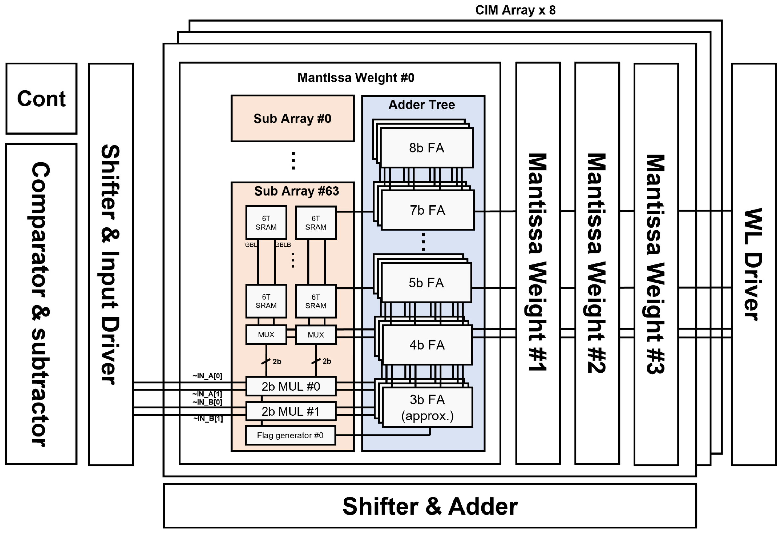
Figure 1 shows the overall mantissa datapath of the proposed BF16 DCIM macro. Weight mantissas are stored in four mantissa weight groups, each consisting of 64 sub-arrays. In each sub-array, the aligned input mantissa and stored weight mantissa are processed in 2-bit segments, and two 2-bit multipliers generate local products. The local products are accumulated through an adder tree, in which the proposed 3-bit approximate adder with flag-based recovery is applied at the first stage. Subsequent higher-stage adders and a shifter-and-adder combine the partial sums to generate the final mantissa-accumulation result.
This study jointly approximates the local multiplier and first-stage adder, which are major contributors to hardware cost in BF16 DCIM mantissa computation. In conventional independent approximation, the errors generated by each operation can overlap during accumulation and degrade accuracy [14,15,16,17,18]. In contrast, the proposed structure intentionally constrains the direction and occurrence condition of the multiplier error, detects whether an error has occurred, and conditionally compensates for it in the first-stage adder.
The exact result of 11 × 11 in 2-bit unsigned multiplication is as follows.
(11)2 × (11)2 = (1001)2 = 9.
The Baseline multiplier approximates this case as 1111, producing the following positive error.
ε_BASE = 15 − 9 = +6.
In this study, the corresponding product is approximated as (0111)2.
ε_PROP = 7 − 9 = −2.
Therefore, the absolute error of the error-inducing multiplication case is reduced from 6 to 2, and the error direction is constrained to be negative. This negative error can be compensated for by injecting a positive carry in the subsequent adder [14,15,16,20]. In contrast, directly compensating for a positive error may require a separate subtraction or borrow operation to remove a value from the result. Thus, a bounded negative error is more suitable for the proposed structure, which uses low-cost carry-in-based recovery [14,15,16,18,20].
Furthermore, among all input combinations of 2-bit unsigned multiplication, the only case in which bit 3 of the product is 1 is 11 × 11 = 1001. Because the proposed multiplier changes this result to 0111, the MSB is 0 for every reachable output generated by the proposed multiplier. Consequently, the first-stage adder does not need to process the fourth multiplier output bit, and the conventional 4-bit product-addition structure can be reduced to an adder structure with 3-bit operands. Thus, the 0111 mapping not only reduces multiplier error but also structurally reduces the cost of the subsequent first-stage adder.
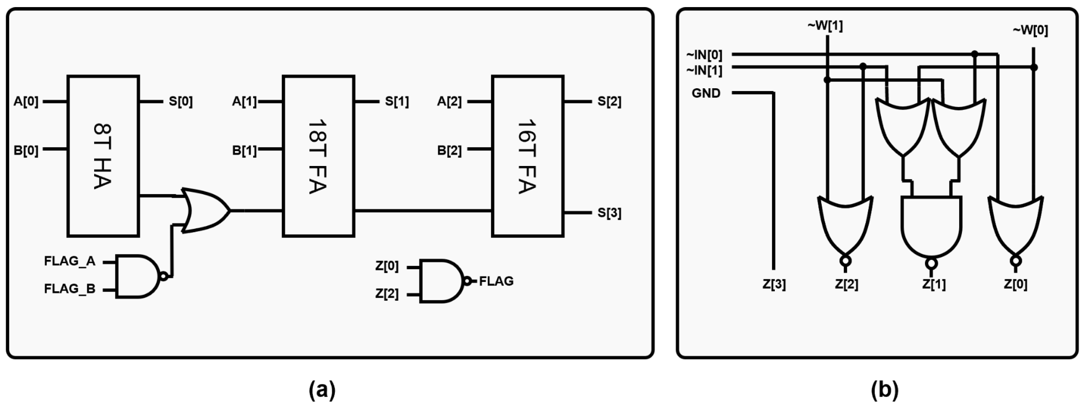
Figure 2 shows the gate-level structures of the proposed multiplier and first-stage recovery adder. The multiplier in Figure 2b generates the product using the complementary inputs I[1:0] and W[1:0]. Z[0] and Z[2] are implemented using NOR gates with I[0], W[0] and I[1], W[1] as their respective inputs. Z[1] is generated by combining the two cross-product terms in an OAI22 form, and Z[3] is tied to GND. The output of the proposed multiplier can therefore be expressed as follows.
Z[0] = ~(~I0 ∨ ~W0) = I0 ∧ W0,
Z[1] = ~[(~W1 ∨ ~I0) ∧ (~W0 ∨ ~I1)] = (I0 ∧ W1) ∨ (I1 ∧ W0),
Z[2] = ~(~I1 ∨ ~W1) = I1 ∧ W1,
Z[3] = 0.
This gate configuration generates only the three valid product bits required for the proposed mapping and removes the Z[3] path that is required for exact multiplication when the inputs are 11 × 11. In particular, instead of cascading two partial-product AND gates followed by a separate OR gate, Z[1] can be integrated into a single OAI logic gate using complementary inputs. Therefore, the 0111 mapping contributes not only to output-width reduction but also to simplification of the internal multiplier logic.
For the 11 × 11 input that produces an approximation error, the output is 0111, and therefore Z[2] and Z[0] are simultaneously 1. Because this condition does not occur for any other output that can be generated by the proposed multiplier, the logical error event E can be detected as follows.
E = Z[2] ∧ Z[0].
In the actual circuit shown in Figure 2a, Z[2] and Z[0] are applied to a NAND gate to generate an active-low flag.
FLAG_N = ~(Z[2] ∧ Z[0]).
Thus, error detection requires only two product bits already generated by the multiplier and one NAND gate, without a separate comparator to re-evaluate the original operands.
Figure 2a shows the proposed first-stage adder that accumulates the outputs of two local multipliers and its flag-based recovery path. Let the 3-bit outputs of the two multipliers be A[2:0] and B[2:0], respectively. The LSBs A[0] and B[0] are processed by an 8T half adder to generate S[0] and carry C0. The active-low flag generated by each multiplier is transferred to the recovery logic. If the two flags are denoted as FLAG_N,A and FLAG_N,B, the active-high recovery signal R, which indicates that an error has occurred in at least one multiplier, is generated as follows.
R = ~(FLAG_N,A ∧ FLAG_N,B) = E_A ∨ E_B.
The generated recovery signal is ORed with the original carry C0 of the LSB half adder and then applied as the carry-in of the 18T FA responsible for bit 1.
C_in,1 = C0 ∨ R.
The 16T FA at bit 2 then generates S[2] and the final carry S[3]. Thus, the proposed first-stage adder consists of an 8T HA, an 18T FA, and a 16T FA, and performs recovery within the existing carry path without a separate multi-bit correction adder.
The error introduced by the 11 × 11 → 0111 mapping is −2; therefore, activating the carry at bit position 1 provides a +2 arithmetic correction. When a single approximation event occurs, and the native carry generated by the LSB half adder is 0, the recovery signal changes the carry input at bit position 1 from 0 to 1, and the −2 multiplier error can be fully compensated. The flag is reused both as a signal indicating the occurrence of an error and as local metadata for generating the correction bit, thereby minimizing the additional datapath required for error detection and recovery [14,15,16].
In contrast, if an approximation event occurs while the native carry is already 1, activating the recovery signal cannot further increase the carry input. In this work, OR saturation denotes this logical condition in which the already-activated carry prevents the 1-bit OR-based recovery path from representing an additional +2 correction. Consequently, a single approximation event under this condition can leave a −2 residual error. When approximation events occur simultaneously in both multipliers, the total multiplier error becomes −4, but the two events are merged into a single binary recovery signal. Because the recovery path cannot represent two independent +2 corrections, a −4 residual error can remain. These incomplete-recovery conditions correspond to the nonzero entries in Table 1.

3.2. Design-Space Exploration

To determine which approximation method is most efficient for local arithmetic in BF16 DCIM, this study conducted a hierarchical design-space exploration of the multiplier and first-stage adder [17,19,25]. Because both operators are repeatedly used in the local computations of the mantissa datapath and account for a substantial portion of the circuit cost, even limited circuit modifications can produce considerable cost reductions. Throughout the exploration, exponent alignment, three-cycle operation, the multiplier-pair configuration, the subsequent accumulation structure, and the 16T/18T full-adder cells were held constant. The independent variables were limited to the exceptional output code of the 2-bit × 2-bit multiplier, the 3FA/4FA architecture of the first-stage adder, and the compensation position. Therefore, the candidates differed only in the multiplier error pattern and first-stage recovery method.
The exploration metrics were divided into arithmetic accuracy and hardware cost [17,18,19,25]. Arithmetic accuracy was evaluated using error rate, mean signed error, absolute bias, RMSE, maximum absolute error, and residual-error rate [17,18,19,25]. For the recovery candidates, full-recovery count and OR-saturation count were also measured. In the initial exhaustive search, the transistor counts of the multiplier, flag, and adder macro were used as hardware-cost proxies. Transistor-level PPA and CNN inference accuracy were then evaluated separately for the final candidate set.
In the first stage, the exceptional output of the 2-bit × 2-bit multiplier for the 11 × 11 input was varied from 0 to 15. Multiplication for the remaining 15 input combinations was fixed to exact multiplication. Because the exact result of 11 × 11 is 9, the multiplier error of exceptional code c was defined as c − 9. For each code, the multiplier transistor count, flag-generation overhead, error polarity and magnitude, and output MSB were compared. Codes 10–15 produce positive multiplier errors, which are difficult to reduce consistently through simple positive carry injection. Instead, positive errors require compensation such as XOR-based correction or adder reduction at the compensation stage. XOR-based compensation can provide precise correction but is more costly than OR-based compensation, whereas adder reduction makes it difficult to control the error magnitude. Therefore, under the proposed positive-carry compensation constraint, negative-error mappings are more suitable.
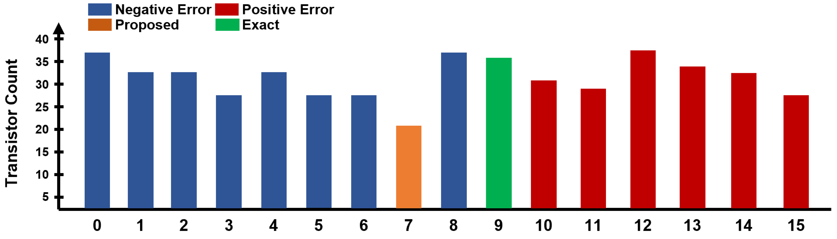
Codes 0–8 produce negative multiplier errors and are therefore directionally compatible with subsequent positive carry compensation. In particular, codes 0–7 always have an output MSB of 0, allowing the first-stage adder to be reduced from 4FA to 3FA. Within this range, code 7 outputs 0111 and produces a bounded error of −2, while exhibiting the lowest circuit cost with a 16T multiplier and a 20T implementation including the flag. Code 8 has a smaller error of −1, but its output MSB is 1 and the multiplier cost increases. Thus, when both multiplier cost and the possibility of adder reduction are considered, code 7 emerges as the primary candidate.
Figure 3 compares the transistor count of the local multiplier for each exceptional output code. Code 7 has a lower circuit cost than code 9, which corresponds to exact multiplication, and fixes the output MSB to 0. It therefore enables both simplification of the multiplier itself and reduction of the first-stage adder to 3FA. Accordingly, when the transistor count and subsequent adder structure are considered together, code 7 is included among the most advantageous candidates.
In the second stage, only the compensation position was varied while each multiplier code was fixed. The evaluated candidates were a structure without compensation, a BIT0 structure that directly applies compensation to the LSB carry-in, and structures that insert OR compensation at BIT1, BIT2, BIT3, or the output bit. All candidates were exhaustively evaluated over the 256 possible input combinations of the two multipliers. This evaluation considered not only the nominal compensation weight but also OR saturation, in which compensation is lost because of a native carry.
Table 2 summarizes the results obtained by varying the compensation position for the code-7 multiplier. The NONE structure without compensation has the lowest circuit cost at 74T, but its residual-error rate remains at 12.109%. BIT0 has the lowest RMSE and maximum error; however, because it injects only +1 for every error event, no complete recovery occurs, and the residual-error rate is not reduced. OR_BIT2 has a mean bias of 0, but this results from cancelation between positive and negative errors, and neither the RMSE nor residual-error rate is improved. In contrast, OR_BIT1 provides compensation with the same weight as the −2 error of the code-7 multiplier, completely recovering 24 of the 31 event cases. It reduces the residual-error rate from 12.109% to 2.734% and the absolute bias from 0.128906 to 0.062500. Its RMSE is approximately 1.27% higher than that of BIT0, but its total transistor count is lower by 2T. Across the complete 256 pair-input combinations, 31 combinations contain at least one Code-7 approximation event; 24 are fully recovered by OR_BIT1, whereas the remaining 7 are limited by the OR-based recovery path and retain a nonzero residual error.
Table 3 compares the principal candidates derived from the design-space exploration with the Exact and Baseline structures over the same local-arithmetic scope. The Proposed structure uses 92T, which is lower than the 156T of the Exact FULL4FA and the 108T of the Baseline 3FA. Its RMSE is approximately 1.27% higher than that of the minimum-RMSE endpoint, code 7 BIT0; however, the residual-error rate decreases from 12.109% to 2.734%, and the absolute bias decreases from 0.128906 to 0.062500. Therefore, the Proposed structure is not a candidate that minimizes only RMSE or transistor count; rather, it is a design point that improves both circuit cost and residual-error characteristics.
The final multiplier code was selected by considering both the exceptional-error magnitude and the possibility of reducing the first-stage adder width. For the exact exceptional multiplication (112 × 112 = 9), the error of an output code c is defined as ε = c − 9; therefore, Codes 6, 7, and 8 correspond to errors of −3, −2, and −1, respectively. Codes 0–7 have a zero output MSB and can therefore retain the reduced first-stage operand width. Among these MSB-zero candidates, Code 7 has the smallest exceptional-error magnitude. Code 8 further reduces the error magnitude to −1, but retains the output MSB and therefore does not provide the same first-stage width reduction.
The compensation position was subsequently evaluated according to its arithmetic correspondence with the multiplier error. The −2 error of Code 7 is directly matched by the +2 correction at bit 1, enabling exact recovery for a large fraction of the error-event cases. By contrast, Code 6 + OR_BIT1 applies only a +2 correction to a −3 error and therefore cannot exactly cancel a single approximation event. Code 8 + BIT0 directly matches its −1 error with a +1 correction and can consequently reduce the numerical error further; however, this configuration retains the multiplier-output MSB and cannot use the reduced first-stage architecture.
The joint DSE comprises 61 Code × compensation configurations evaluated exhaustively over all 256 multiplier-pair inputs. Code 7 + OR_BIT1 achieves a normalized RMSE of 2.1960% and a residual-error rate of 2.734%, with 24 full-recovery cases at an analytical structural cost of 92T. Code 8 + BIT0 further reduces the normalized RMSE to 0.3472% and the residual-error rate to 0.391%. However, because Code 8 retains the output MSB and does not enable the first-stage width reduction, its analytical structural cost increases to 122T, 30T higher than the Proposed configuration. Code 6 + OR_BIT1, in comparison, requires 104T, with a normalized RMSE of 2.3550% and a residual-error rate of 12.109%.
Table 4 summarizes representative hardware–error trade-offs in the joint code–compensation design space.
Accordingly, the final design point was selected based on the combined hardware–error trade-off rather than arithmetic-error minimization alone. Code 7 + OR_BIT1 preserves the reduced first-stage architecture and maintains substantially lower structural cost than the lower-error Code 8 alternative, while reducing the residual-error rate from 12.109% without compensation to 2.734%. Thus, the selected configuration provides the hardware reduction targeted by the joint multiplier–adder approximation while retaining effective error control.

4. Evaluation and Analysis

4.1. Evaluation Setup and Baseline

The Baseline local arithmetic unit used in this study was reconstructed from the BF16 DCIM arithmetic organization reported in [11]. In the published Baseline macro [11], the upper six bits of the 7-bit fraction of the BF16 weight mantissa, excluding the LSB, are divided into 2-bit segments and processed over three cycles. For the local circuit comparison, the overall datapath, including exponent alignment, three-cycle operation, and the accumulation structure, was kept consistent with the published architecture, and the compared arithmetic units are explicitly denoted as Exact, Baseline, and Proposed.
The Baseline and Proposed designs are not evaluated as two independently redesigned BF16 DCIM macros. The exponent-alignment scheme, three-cycle mantissa processing, multiplier-pair organization, and subsequent higher-stage accumulation are retained consistently with the published Baseline architecture, while the structural modification is concentrated in the local 2-bit × 2-bit multiplier and first-stage pair-adder boundary. The Proposed flag-generation and carry-recovery circuitry are also included within this local replacement boundary. Accordingly, the macro-level significance of the local circuit-level PPA can be examined from the replication of this arithmetic boundary in the published Baseline hierarchy.
The circuit-level comparison evaluates a common local arithmetic boundary consisting of two 2-bit × 2-bit multipliers and one first-stage pair adder, including the flag-generation and carry-recovery circuitry in the Proposed design. The arithmetic units were implemented at the transistor level in Cadence Virtuoso and evaluated using Spectre transient simulation in a 28 nm technology. Transistor count is used as a circuit-complexity-based area proxy rather than as a physical layout-area measurement. The nominal circuit-level comparison is performed at 1.0 V under the TT/25 °C condition. For the nominal power and energy comparison, the same 64-vector sequence is applied for 5 ns per vector with 50 ps input rise/fall times, for a total simulation interval of 320 ns.
CIFAR-10 and CIFAR-100 are 32 × 32 color-image classification datasets containing 60,000 images each, with 10 and 100 classes, respectively; each dataset contains 50,000 training images and 10,000 test images. Inference accuracy was evaluated on all 10,000 test images in each dataset using pretrained ResNet18, VGG16-BN, and AlexNet checkpoints.
To provide a controlled comparison with external approximate-arithmetic schemes, representative approximation mechanisms from DIMC and LSAC were functionally emulated within the same BF16 evaluation framework. DIMC-S-derived applies the single-approximate compressor mechanism [23], whereas LSAC OR+SXAFA-derived applies the OR+SXAFA approximate-adder-tree mechanism [24]. The same pretrained checkpoints, preprocessing, test-sample order, and BF16 reference were used for all schemes. Accordingly, this comparison evaluates the numerical behavior of the approximation mechanisms under a common BF16 workload rather than reproducing the native macros or their complete software co-design procedures.
Numerical error was evaluated using Layer normalized root mean square error (NRMSE) and Logit NRMSE against the same BF16 reference. Layer NRMSE was evaluated for Conv2d and Linear outputs over a fixed 64-image diagnostic subset, whereas Logit NRMSE and Top-1 accuracy were evaluated over the complete 10,000-image test set of each dataset.

4.2. PPA Evaluation

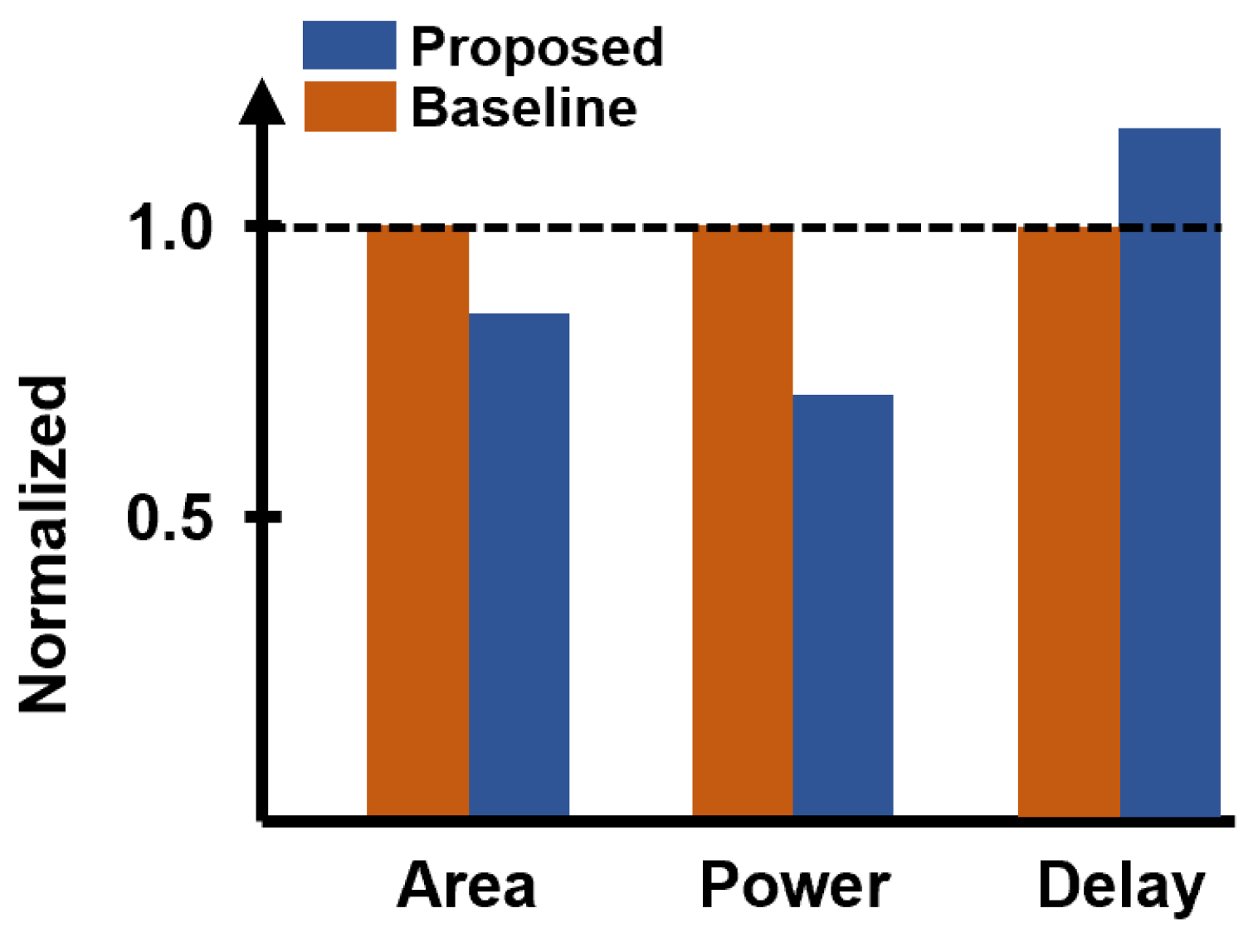
Table 5 compares the circuit-level implementation results of the Exact, Baseline, and Proposed arithmetic units over the common local boundary. The transistor counts of the Exact, Baseline, and Proposed structures are 156T, 108T, and 92T, respectively; thus, the Proposed structure reduces the transistor count by 14.81% relative to the Baseline. The normalized area proxy likewise decreases from 0.692 for the Baseline to 0.590 for the Proposed structure.
The average power was measured as 1.71, 1.40, and 1.00 μW for the Exact, Baseline, and Proposed structures, respectively, and the Proposed structure consumed 28.56% less power than the Baseline. Over the same 320 ns, 64-vector sequence, the total supply energy decreased from 449.33 fJ for the Baseline to 321.00 fJ for the Proposed design. This result directly quantifies the energy advantage of the repeated local arithmetic boundary; the actual complete-macro energy reduction additionally depends on the switching activity of global circuitry, interconnect capacitance, and physical integration and is therefore not directly extrapolated from the local value.
At the nominal TT/1.0 V/25 °C condition, the worst propagation delays of the Baseline and Proposed local pair-arithmetic units are 46.589 ps and 54.602 ps, respectively. The Proposed design therefore introduces an absolute delay increase of 8.013 ps, corresponding to a 17.20% relative local delay overhead.
The same local timing boundary was further evaluated under representative PVT conditions. The Proposed-to-Baseline delay overheads are 18.67%, 16.30%, 17.20%, 16.38%, and 16.28% for SSF/0.9 V/125 °C, SSF/0.9 V/−40 °C, TT/1.0 V/25 °C, FFF/1.1 V/125 °C, and FFF/1.1 V/−40 °C, respectively. The maximum Proposed delay within the evaluated set is 98.568 ps. These results show that the relative local timing penalty remains within a narrow 16.28–18.67% range across the evaluated PVT conditions.
For macro-level timing interpretation, the absolute delay increment provides a more meaningful scale than directly applying the 17.20% local percentage to the macro clock frequency. The published Baseline shmoo includes a passing operating point at 205 MHz and 0.9 V [11], corresponding to a clock period of approximately 4.878 ns. The nominal 8.013 ps local delay increment is approximately 0.164% of this demonstrated clock-period scale. Therefore, the 17.20% relative delay increase observed inside the local arithmetic boundary does not correspond to an equivalent 17.20% reduction in macro operating frequency or throughput.
In addition, the Proposed arithmetic replacement preserves the Baseline three-cycle mantissa-processing schedule [11] and introduces no additional processing cycle or pipeline stage. Thus, the Proposed structure does not add cycle-level latency at the architectural level. The PVT results indicate a consistent local timing cost, while its absolute increment remains small relative to the demonstrated macro clock-period scale; accordingly, the local delay penalty is treated as a timing cost of the replacement boundary rather than as an equivalent macro-throughput penalty.
Table 6 summarizes the representative PVT timing results for the local pair-arithmetic unit.
The published Baseline contains eight CIM arrays, and three of the four mantissa-weight blocks in each array process non-sign 2-bit mantissa segments, while the remaining block implements the sign path. Because each non-sign block contains 64 2-bit multipliers, the published non-sign datapath affected by the Proposed structure contains a total of 1536 2-bit multipliers and 768 first-stage multiplier-pair boundaries [11].
In the present circuit-level comparison, one replacement boundary consists of two 2-bit multipliers and one first-stage pair adder, with transistor counts of 108T for the Baseline and 92T for the Proposed design. Replicating the same local implementation over the 768 pair boundaries identified in the published hierarchy gives transistor-count proxies of 82,944T and 70,656T, respectively. This corresponds to a reduction of 12,288T, or 14.81%, showing that the measured local reduction ratio is preserved when the replacement boundary is propagated through the repeated arithmetic hierarchy.
The first stage of the published six-stage Baseline adder tree consists of 32 three-bit pair adders. In terms of logical adder-bit instances, this stage contains 96 of the 246 instances in the approximate tree, corresponding to approximately 39.0%. Thus, the Proposed modification targets the most highly replicated stage of the adder tree rather than an isolated arithmetic element.
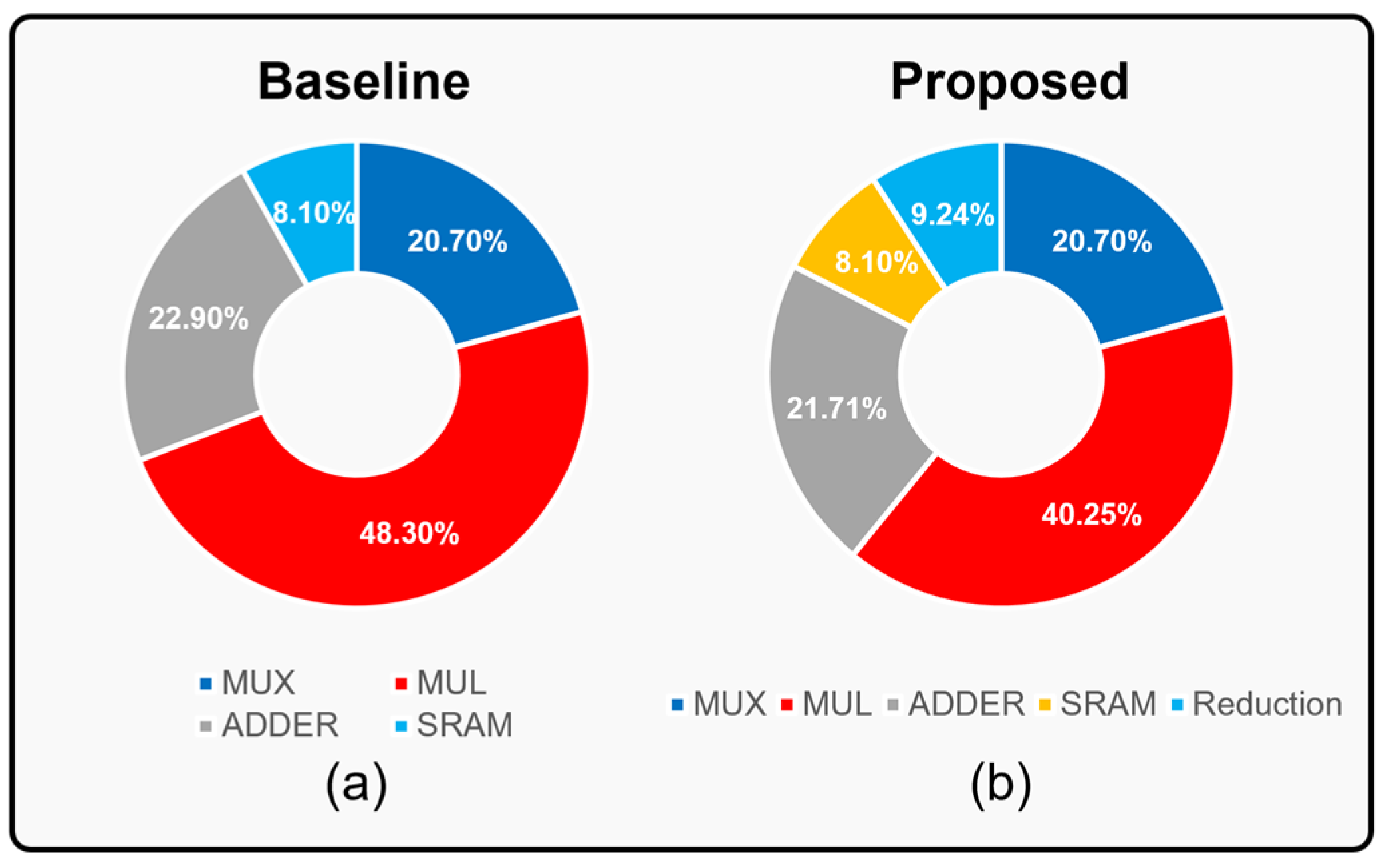
The reported compute/memory composition in Baseline Figure 4 assigns 20.7%, 48.3%, 22.9%, and 8.1% to MUX, MUL, ADDER, and SRAM, respectively [11], indicating that multiplier and adder circuitry are major hardware-cost components of the reported compute structure. When the measured implementation reductions of the multiplier and first-stage adder are combined with the topology-derived first-stage contribution, the resulting first-order hardware-cost proxy corresponds to an approximately 9.2% reduction in the four-category composition reported in Baseline Figure 4. This value is an architecture-derived area proxy obtained from the published topology and measured local transistor-count ratios, rather than a post-layout measurement of the complete macro.
Figure 4 visualizes the published Baseline hardware composition and the corresponding first-order Proposed composition after applying the architecture-derived reduction proxy. Figure 5 summarizes the normalized local area-proxy, average-power, and propagation-delay comparison between the Baseline and Proposed arithmetic units.

4.3. Numerical Error and Inference Accuracy

Table 7 compares the numerical error of the Baseline, DIMC-S-derived, LSAC OR+SXAFA-derived, and Proposed schemes under the same BF16 reference and CNN workloads. Unlike the previous local-RMSE evaluation, the revised comparison uses Layer NRMSE and Logit NRMSE so that approximation mechanisms with different arithmetic boundaries can be evaluated using a common numerical reference. The Proposed scheme achieves the lowest Layer NRMSE and Logit NRMSE among the four evaluated schemes for ResNet18, VGG16-BN, and AlexNet on both CIFAR-10 and CIFAR-100.
Relative to DIMC-S-derived, the Proposed scheme reduces Layer NRMSE by 61.85–80.55% and Logit NRMSE by 35.30–63.13%. Relative to LSAC OR+SXAFA-derived, the corresponding reductions are 28.43–58.64% and 8.14–33.75%, respectively. The layer-call NRMSE distributions show the same trend, with the Proposed scheme exhibiting the lowest median, P95, and maximum values in all six model–dataset combinations. Thus, the reduction in aggregate numerical error is consistently observed across the layer-wise error distribution.
The 256-case exhaustive analysis in Section 3.2 characterizes the structural residual behavior of the Proposed recovery logic, but it does not represent how often each local operand combination occurs in a trained CNN workload. To quantify workload-level behavior, the existing BF16 inference path was additionally instrumented to count the 2-bit local operands after exponent alignment for all 10,000 test images of CIFAR-10 and CIFAR-100 using ResNet18, VGG16-BN, and AlexNet. The instrumentation only observes the operands and does not alter the arithmetic path; the instrumented runs reproduced the previously obtained Proposed logits and Top-1 results.
Exceptional MUL is normalized by the number of individual local multiplier operations. Flagged Pair and Residual/Pair are normalized by the number of local pair operations scheduled in the fixed group-64 arithmetic datapath, including zero-padded lanes used to complete an incomplete group. Full Recovery/Flag and OR Saturation/Flag use flagged pairs as the denominator. The observed nonzero residuals (−2 and −4) are unscaled first-stage local arithmetic residuals before sign, positional weighting, and exponent scaling.
As shown in Table 8, exceptional 112 × 112 multiplier events occurred in 0.368–0.638% of individual multiplier operations, while at least one error flag was raised in 0.726–1.254% of scheduled local pair operations. Among flagged pairs, 80.50–88.53% were fully recovered through the bit-1 carry compensation, whereas 11.47–19.50% corresponded to OR saturation. Consequently, the empirical nonzero residual-event rate was 0.083–0.220% of scheduled local pairs. In all six model–dataset configurations, the residual-event count exactly matched the OR-saturation count, and all observed nonzero local residuals were limited to −2 or −4. Accordingly, the 2.734% value from the uniform 256-case evaluation is interpreted as an exhaustive-domain residual rate rather than the occurrence probability of residual errors in an actual CNN workload.
The full-workload layer-wise aggregation showed workload-dependent variation in local event frequency but no monotonic trend with network depth. When the three activation-mantissa processing cycles were grouped as XH, XM, and XL, the residual-event frequency increased from XH to XM to XL in all six evaluated model–dataset configurations. Because each activation-cycle bucket aggregates cross-products with WH, WM, and WL, this result is used only as an event-frequency trend and not as a direct measure of numerical significance. Sign, individual exponent shift, channel, accumulation depth, and zero/denormal category were not independently stratified; therefore, no conditional error-bias claim is made for these categories.
Table 9 compares the Top-1 inference accuracy of the four schemes under the same workloads. The Proposed scheme achieves higher Top-1 accuracy than DIMC-S-derived and LSAC OR+SXAFA-derived in all six model–dataset combinations. Relative to the Baseline, the difference remains within −0.02 to +0.12 percentage points. Accordingly, the results are interpreted as reduced numerical distortion with inference accuracy comparable to the Baseline rather than as a general improvement in inference accuracy.

5. Discussion

Although this study directly evaluates the mantissa datapath of BF16 DCIM, the fundamental design objective of the proposed structure is not limited to a particular data format or CIM architecture. In various arithmetic units dominated by repeated MAC operations, multipliers and accumulation circuits are major contributors to area and power. Some conventional approximate-arithmetic methods combine circuit simplification with software-level processing, such as retraining, pruning, data mapping, or number formats designed for approximate arithmetic, to mitigate the resulting accuracy degradation [21,23,24]. These methods can provide high efficiency optimized for particular models and data distributions, but additional preprocessing and calibration may be required when they are applied to pretrained models or other input distributions. In contrast, this study aims to constrain the sign and occurrence condition of multiplication errors within the hardware and apply the same local compensation rule to every operation without separate software modification. Therefore, the main objective of this study is not merely to reduce error for a particular workload, but to explicitly control the relationship among error generation, detection, and compensation at the circuit level.
In the common-BF16 evaluation, the Proposed scheme exhibits lower Layer NRMSE and Logit NRMSE than the Baseline, DIMC-S-derived, and LSAC OR+SXAFA-derived schemes in all six model–dataset combinations, with the same trend observed across the layer-call NRMSE distributions. However, because the Top-1 difference relative to the Baseline remains within −0.02 to +0.12 percentage points, the numerical-error reduction is not interpreted as a general improvement in inference accuracy. The DIMC-S-derived and LSAC OR+SXAFA-derived results represent mechanism-level functional comparisons under the common BF16 workload.
The Proposed approximation–detection–compensation structure does not necessarily guarantee simultaneous improvements in area, power, and delay. The error-detection and compensation paths can introduce additional logic, wiring, and critical-path overhead [14,15,16,20]. At TT/1.0 V/25 °C, the Proposed local pair-arithmetic delay is 54.602 ps compared with 46.589 ps for the Baseline, an absolute increase of 8.013 ps and a relative increase of 17.20%. Across the five evaluated PVT conditions, the relative local delay overhead remains within 16.28–18.67%, with a maximum Proposed delay of 98.568 ps. These values characterize the local replacement boundary and are not measured complete-macro Fmax or throughput degradations. The published Baseline passing point of 205 MHz at 0.9 V [11] provides only a timing-scale reference: the nominal 8.013 ps increment is approximately 0.164% of the corresponding 4.878 ns clock period, and the Proposed design preserves the same three-cycle mantissa-processing schedule without adding a pipeline stage. Complete-macro critical-path timing, explicit next-stage loading, extracted routing parasitics, PVT-dependent power/energy, energy-delay product, and transistor-level Monte Carlo variation remain outside the direct measurement scope.
Despite these limitations, the directly measured local transistor count and average power are reduced by 14.81% and 28.56%, respectively, relative to the Baseline. The architecture-derived composition analysis further indicates an approximately 9.24% first-order hardware-cost reduction within the four-category composition reported for the published Baseline, but this value is an area proxy rather than a complete-macro post-layout measurement. The compensation is implemented by reusing the 1-bit flag in the existing carry path rather than by adding a separate multi-bit correction circuit; thus, the main benefit is the combined reduction in local circuit cost and BF16-referenced numerical distortion while maintaining inference accuracy comparable to the Baseline.
Future work should extend the current joint-design scope, which is limited to the multiplier and first adder stage, to the entire MAC datapath. For example, not only the approximate output value and the weight and position of the compensation bit, but also mantissa significance, adder-tree stage, accumulation depth, sign processing, and normalization could be included as joint exploration variables. It is also necessary to compare the current approach, which applies identical compensation at every position, with a selective approach that controls compensation according to the layer or cycle under the same hardware constraints. Such an extended exploration is not simply a matter of selecting the smallest multiplier or adder; rather, it must determine where errors should be introduced, through which signals they should be transferred, and at which stage they should be compensated to provide the most favorable balance between overall circuit cost and accuracy [17,19,25]. However, because the current results are limited to local arithmetic units in BF16 DCIM and CNNs based on CIFAR-10 and CIFAR-100, further verification is required to determine whether these design principles provide the same benefits in other MAC structures.

6. Conclusions

This study proposed an error-recoverable arithmetic structure that jointly approximates the 2-bit multiplier and first adder stage in BF16 digital compute-in-memory mantissa computation. The Proposed multiplier maps the exceptional 11 × 11 result to 0111, changing the Baseline error from +6 to −2 and fixing the product MSB to 0 so that the first-stage adder can be reduced from 4 bits to 3 bits. A lightweight flag detects the error-inducing condition and is directly reused in the existing bit-1 carry path to provide conditional compensation without a separate multi-bit correction circuit. Transistor-level evaluation of the common local arithmetic boundary showed 14.81% and 28.56% reductions in transistor count and average power, respectively, relative to the Baseline, while the nominal propagation delay increased by 17.20%; across the evaluated PVT conditions, the relative local delay overhead remained within 16.28–18.67%. The architecture-derived composition analysis gives an approximately 9.24% first-order hardware-cost proxy, which is not a complete-macro post-layout result. Under the common-BF16 evaluation, the Proposed scheme achieved the lowest Layer NRMSE and Logit NRMSE among the Baseline, DIMC-S-derived, LSAC OR+SXAFA-derived, and Proposed schemes for all six ResNet18, VGG16-BN, and AlexNet model–dataset combinations on CIFAR-10 and CIFAR-100. The Top-1 accuracy difference relative to the Baseline remained within −0.02 to +0.12 percentage points. Therefore, the Proposed structure provides a balanced hardware–accuracy design point that reduces local circuit cost and BF16-referenced numerical distortion while maintaining inference accuracy comparable to the Baseline, without retraining or data rearrangement. Future work should include post-layout parasitics, flag-routing load, complete-macro timing and energy evaluation, and an extended joint-design exploration covering higher adder-tree stages.

Author Contributions

Conceptualization, Y.J. and M.K.; methodology, Y.J. and M.K.; software, Y.J.; validation, Y.J. and M.K.; formal analysis, Y.J.; investigation, Y.J.; data curation, Y.J.; visualization, Y.J.; writing—original draft preparation, Y.J.; writing—review and editing, M.K.; supervision, M.K.; project administration, M.K.; funding acquisition, M.K. All authors have read and agreed to the published version of the manuscript.

Funding

This work was supported by the National Research Foundation of Korea (NRF) grant funded by the Korea government (MSIT) (No. RS-2026-25536380). The EDA tool was supported by the IC Design Education Center (IDEC), Korea. This work was supported by Seoul National University of Science and Technology.

Data Availability Statement

The raw data supporting the conclusions of this article will be made available by the authors on request.

Conflicts of Interest

The authors declare no conflicts of interest.

References

  1. Horowitz, M. 1.1 Computing’s Energy Problem (and What We Can Do About It). In Proceedings of the 2014 IEEE International Solid-State Circuits Conference (ISSCC), San Francisco, CA, USA, 9–13 February 2014; pp. 10–14. [Google Scholar] [CrossRef] [Scilit]
  2. Sze, V.; Chen, Y.-H.; Yang, T.-J.; Emer, J.S. Efficient Processing of Deep Neural Networks: A Tutorial and Survey. Proc. IEEE 2017, 105, 2295–2329. [Google Scholar] [CrossRef] [Scilit]
  3. Verma, N.; Jia, H.; Valavi, H.; Tang, Y.; Ozatay, M.; Chen, L.-Y.; Zhang, B.; Deaville, P. In-Memory Computing: Advances and Prospects. IEEE Solid-State Circuits Mag. 2019, 11, 43–55. [Google Scholar] [CrossRef] [Scilit]
  4. Si, X.; Tu, Y.-N.; Huang, W.-H.; Su, J.-W.; Lu, P.-J.; Wang, J.-H.; Liu, T.-W.; Wu, S.-Y.; Liu, R.; Chou, Y.-C.; et al. A 28 nm 64 Kb 6T SRAM Computing-in-Memory Macro with 8b MAC Operation for AI Edge Chips. In Proceedings of the 2020 IEEE International Solid-State Circuits Conference (ISSCC), San Francisco, CA, USA, 16–20 February 2020; pp. 246–248. [Google Scholar] [CrossRef] [Scilit]
  5. Chih, Y.-D.; Lee, P.-H.; Fujiwara, H.; Shih, Y.-C.; Lee, C.-F.; Naous, R.; Chen, Y.-L.; Lo, C.-P.; Lu, C.-H.; Mori, H.; et al. An 89 TOPS/W and 16.3 TOPS/mm2 All-Digital SRAM-Based Full-Precision Compute-In-Memory Macro in 22 nm for Machine-Learning Edge Applications. In Proceedings of the 2021 IEEE International Solid-State Circuits Conference (ISSCC), San Francisco, CA, USA, 13–22 February 2021; pp. 252–254. [Google Scholar] [CrossRef] [Scilit]
  6. Henry, G.; Tang, P.T.P.; Heinecke, A. Leveraging the bfloat16 Artificial Intelligence Datatype for Higher-Precision Computations. In Proceedings of the 26th IEEE Symposium on Computer Arithmetic (ARITH), Kyoto, Japan, 10–12 June 2019; pp. 69–76. [Google Scholar] [CrossRef] [Scilit]
  7. Tu, F.; Wang, Y.; Wu, Z.; Liang, L.; Ding, Y.; Kim, B.; Liu, L.; Wei, S.; Xie, Y.; Yin, S. ReDCIM: Reconfigurable Digital Computing-In-Memory Processor with Unified FP/INT Pipeline for Cloud AI Acceleration. IEEE J. Solid-State Circuits 2023, 58, 243–255. [Google Scholar] [CrossRef] [Scilit]
  8. Guo, A.; Si, X.; Chen, X.; Dong, F.; Pu, X.; Li, D.; Zhou, Y.; Ren, L.; Xue, Y.; Dong, X.; et al. A 28 nm 64-kb 31.6-TFLOPS/W Digital-Domain Floating-Point-Computing-Unit and Double-Bit 6T-SRAM Computing-in-Memory Macro for Floating-Point CNNs. In Proceedings of the 2023 IEEE International Solid-State Circuits Conference (ISSCC), San Francisco, CA, USA, 19–23 February 2023; pp. 128–130. [Google Scholar] [CrossRef] [Scilit]
  9. Wu, P.-C.; Su, J.-W.; Hong, L.-Y.; Ren, J.-S.; Chien, C.-H.; Chen, H.-Y.; Ke, C.-E.; Hsiao, H.-M.; Li, S.-H.; Sheu, S.-S.; et al. A 22 nm 832 Kb Hybrid-Domain Floating-Point SRAM In-Memory-Compute Macro with 16.2–70.2 TFLOPS/W for High-Accuracy AI-Edge Devices. In Proceedings of the 2023 IEEE International Solid-State Circuits Conference (ISSCC), San Francisco, CA, USA, 19–23 February 2023; pp. 126–128. [Google Scholar] [CrossRef] [Scilit]
  10. Lin, C.-T.; Oh, J.; Seok, M. STAR-SRAM: 16-bit Floating-Point SRAM-Based Digital Computing-in-Memory Macro in a 28 nm. IEEE J. Solid-State Circuits 2026, 1–13. [Google Scholar] [CrossRef] [Scilit]
  11. Kim, J.; Kim, H.; Lee, Y. A 28 nm 77.2 TFLOPS/W Digital Floating-Point Compute-In-Memory Macro Employing Dynamic Find-Max and Reduced-Cycle Bit-Serial Architecture with Approximation. In Proceedings of the 2025 IEEE Asian Solid-State Circuits Conference (A-SSCC), Daejeon, Republic of Korea, 2–5 November 2025; pp. 142–144. [Google Scholar] [CrossRef] [Scilit]
  12. Xu, Q.; Mytkowicz, T.; Kim, N.S. Approximate Computing: A Survey. IEEE Des. Test 2016, 33, 8–22. [Google Scholar] [CrossRef] [Scilit]
  13. Momeni, A.; Han, J.; Montuschi, P.; Lombardi, F. Design and Analysis of Approximate Compressors for Multiplication. IEEE Trans. Comput. 2015, 64, 984–994. [Google Scholar] [CrossRef] [Scilit]
  14. Ha, M.; Lee, S. Multipliers with Approximate 4–2 Compressors and Error Recovery Modules. IEEE Embed. Syst. Lett. 2018, 10, 6–9. [Google Scholar] [CrossRef] [Scilit]
  15. Liu, C.; Han, J.; Lombardi, F. A Low-Power, High-Performance Approximate Multiplier with Configurable Partial Error Recovery. In Proceedings of the 2014 Design, Automation and Test in Europe Conference and Exhibition (DATE), Dresden, Germany, 24–28 March 2014; pp. 1–4. [Google Scholar] [CrossRef] [Scilit]
  16. Jiang, H.; Liu, C.; Lombardi, F.; Han, J. Low-Power Approximate Unsigned Multipliers with Configurable Error Recovery. IEEE Trans. Circuits Syst. I Regul. Pap. 2019, 66, 189–202. [Google Scholar] [CrossRef] [Scilit]
  17. Strollo, A.G.M.; Napoli, E.; De Caro, D.; Petra, N.; Di Meo, G. Comparison and Extension of Approximate 4–2 Compressors for Low-Power Approximate Multipliers. IEEE Trans. Circuits Syst. I Regul. Pap. 2020, 67, 3021–3034. [Google Scholar] [CrossRef] [Scilit]
  18. Hashemi, S.; Bahar, R.I.; Reda, S. DRUM: A Dynamic Range Unbiased Multiplier for Approximate Applications. In Proceedings of the 2015 IEEE/ACM International Conference on Computer-Aided Design (ICCAD), Austin, TX, USA, 2–6 November 2015; pp. 418–425. [Google Scholar] [CrossRef] [Scilit]
  19. Strollo, A.G.M.; Napoli, E.; De Caro, D.; Petra, N.; Saggese, G.; Di Meo, G. Approximate Multipliers Using Static Segmentation: Error Analysis and Improvements. IEEE Trans. Circuits Syst. I Regul. Pap. 2022, 69, 2449–2462. [Google Scholar] [CrossRef] [Scilit]
  20. Sabetzadeh, F.; Moaiyeri, M.H.; Ahmadinejad, M. An Ultra-Efficient Approximate Multiplier with Error Compensation for Error-Resilient Applications. IEEE Trans. Circuits Syst. II Express Briefs 2023, 70, 776–780. [Google Scholar] [CrossRef] [Scilit]
  21. Kumari, A.; Palathinkal, R.P. Design and Analysis of Energy Efficient Approximate Multipliers for Image Processing and Deep Neural Network. IEEE Trans. Circuits Syst. I Regul. Pap. 2025, 72, 854–867. [Google Scholar] [CrossRef] [Scilit]
  22. Guo, R.; Chen, X.; Wang, L.; Tu, F.; Wei, S.; Hu, Y.; Yin, S. A 28 nm 4170-TFLOPS/W/b and 195-TFLOPS/mm2/b Multiply-Free Fully-Digital Floating-Point Compute-In-Memory Macro with Mitchell’s Approximation. In Proceedings of the 2024 IEEE Symposium on VLSI Technology and Circuits, Honolulu, HI, USA, 16–20 June 2024; pp. 1–2. [Google Scholar] [CrossRef] [Scilit]
  23. Wang, D.; Lin, C.-T.; Chen, G.K.; Knag, P.; Krishnamurthy, R.K.; Seok, M. DIMC: 2219 TOPS/W 2569F2/b Digital In-Memory Computing Macro in 28 nm Based on Approximate Arithmetic Hardware. In Proceedings of the 2022 IEEE International Solid-State Circuits Conference (ISSCC), San Francisco, CA, USA, 20–24 February 2022; pp. 266–268. [Google Scholar] [CrossRef] [Scilit]
  24. He, C.; Wang, Z.; Xiang, F.; Dai, Z.; He, Y.; Yue, J.; Liu, Y. LSAC: A Low-Power Adder Tree for Digital Computing-in-Memory by Sparsity and Approximate Circuits Co-Design. IEEE Trans. Circuits Syst. II Express Briefs 2024, 71, 852–856. [Google Scholar] [CrossRef] [Scilit]
  25. Napoli, E.; Zacharelos, E.; Strollo, A.G.M.; Di Meo, G. Approximate Full-Adders: A Comprehensive Analysis. IEEE Access 2024, 12, 136054–136072. [Google Scholar] [CrossRef] [Scilit]
Figure 1. Overall architecture of the proposed error-recoverable BF16 digital computing-in-memory macro.
Electronics 15 03861 g001
Figure 2. Proposed local arithmetic circuits: (a) flag-based approximate first-stage adder; (b) 2-bit × 2-bit approximate multiplier and flag generator.
Electronics 15 03861 g002
Figure 3. Transistor-count comparison across the explored local multiplier codes.
Electronics 15 03861 g003
Figure 4. Hardware composition of the Baseline and Proposed designs: (a) Baseline composition; (b) Proposed composition including the architecture-derived 9.24% hardware reduction.
Electronics 15 03861 g004
Figure 5. Normalized area, power, and delay comparison between the Baseline and Proposed local arithmetic units.
Electronics 15 03861 g005
Table 1. Output error for valid first-stage adder input combinations.
A\B0000000100100011010001100111
00000000000
0001000000−2
00100000000
0011000000−2
01000000000
01100000000
01110−20−200−4
−2/−4: residual error magnitude; 0: recovered or error-free output.
Table 2. Code 7 compensation-placement comparison.
PlacementTotal TransistorsNormalized
RMSE (%)
Residual Error Rate (%)Absolute
Bias
Maximum
Error
Full
Recovery
OR
Saturation
NONE744.049312.109%0.250000400
BIT0942.168412.109%0.128906300
OR_BIT1 (Proposed)922.19602.734%0.0625004247
OR_BIT2924.049312.109%0.0000004015
OR_BIT3928.391012.109%0.1875006017
OR_OUTPUT49226.949512.109%1.6875001400
The RMSE was normalized by the maximum exact sum of two 2-bit multiplication results, i.e., 18. The selected Proposed configuration is shown in bold.
Table 3. Final local-arithmetic architecture comparison.
ArchitectureTotal TransistorsRMSE (%)Absolute
Bias
Maximum
Error
Role
Exact FULL4FA1560.000.000Exact endpoint
Baseline 3FA1082.170.133Baseline
Code 7 NONE744.050.254Minimum-cost endpoint
Code 7 BIT0942.170.133Minimum-RMSE endpoint
Proposed: Code 7 + OR_BIT1922.200.064Selected design point
The selected Proposed design point is shown in bold.
Table 4. Representative hardware–error trade-offs in the joint code–compensation design space.
ConfigurationError
ε
Analytical
Cost (T) *
Normalized
RMSE (%)
Residual
Error Rate
Absolute
Bias
Maximum
Error
Full
Recovery
OR
Saturation
Code 6 + OR_BIT1−31042.355012.109%0.132812400
Code 7 + NONE−2744.049312.109%0.250000400
Code 7 + BIT0−2942.168412.109%0.128906300
Code 7 + OR_BIT1 (Proposed)−2922.19602.734%0.0625004247
Code 8 + NONE−11102.024612.109%0.125000200
Code 8 + BIT0−11220.34720.391%0.0039061300
Code 8 + OR_BIT1−11201.901811.719%0.117188110
* Analytical Cost (T): DSE transistor-count proxy, not measured area/PPA. Code 8 retains the output MSB; NRMSE is normalized by 18. The selected Proposed configuration is shown in bold; additional bold values indicate the best numerical-error/recovery metrics among the listed alternatives.
Table 5. Circuit-level implementation metrics for the local arithmetic unit.
DesignTransistor CountNormalized AreaAverage
Power (µW)
Normalized PowerEnergy (fJ)Worst-Case Propagation Delay (ps)
Exact1561.0001.711.00546.4075.457
Baseline1080.6921.400.82449.3346.589
Proposed920.5901.000.59321.0054.602
Transistor count is used as an area proxy. Area and power are normalized to the Exact implementation. Energy is the total supply energy over the common 64-vector input sequence. Best values for each metric are shown in bold.
Table 6. Representative PVT timing evaluation of the local pair-arithmetic unit.
PVT ConditionBaseline Worst Delay (ps)Proposed Worst Delay (ps)Proposed vs. Baseline
SSF/0.9 V/125 °C64.13576.108+18.67%
SSF/0.9 V/−40 °C84.75498.568+16.30%
TT/1.0 V/25 °C46.58954.602+17.20%
FFF/1.1 V/125 °C33.27938.729+16.38%
FFF/1.1 V/−40 °C34.78140.443+16.28%
Table 7. BF16-referenced NRMSE comparison under common CNN workloads.
DatasetModelBaselineDIMC-S-DerivedLSAC OR+SXAFA-DerivedProposed
CIFAR-10ResNet183.321/4.78710.632/9.2056.896/6.1653.230/4.634
CIFAR-10VGG16-BN2.940/5.33314.684/13.5296.906/5.6482.856/5.086
CIFAR-10AlexNet3.106/5.1447.913/13.0544.218/7.0663.019/5.018
CIFAR-100ResNet183.135/9.2999.672/14.0456.318/9.8923.050/9.087
CIFAR-100VGG16-BN3.185/7.59113.782/19.8547.466/11.0503.094/7.321
CIFAR-100AlexNet5.750/9.58914.870/18.58710.293/11.3765.636/9.225
Layer/Logit NRMSE (%). Layer: fixed 64-image Conv2d/Linear diagnostic; Logit: full 10,000-image test set. BF16 reference; lower is better. Best values in each row are shown in bold.
Table 8. Workload-level occurrence and recovery statistics for the Proposed arithmetic unit.
DatasetModelExceptional MUL (%)Flagged Pair (%)Full Recovery/Flag (%)OR Saturation/Flag (%)Residual/Pair (%)
CIFAR-10ResNet180.4270.84287.32412.6760.107
CIFAR-10VGG16-BN0.3680.72688.52811.4720.083
CIFAR-10AlexNet0.6381.25485.71514.2850.179
CIFAR-100ResNet180.4270.84187.08712.9130.109
CIFAR-100VGG16-BN0.4050.79987.86012.1400.097
CIFAR-100AlexNet0.5841.12880.50319.4970.220
Denominators: MUL = individual operations; Pair = scheduled pairs (including zero padding); Recovery/Saturation = flagged pairs. Residuals are unscaled local errors (−2/−4).
Table 9. Top-1 inference-accuracy comparison under the common BF16 workloads.
DatasetModelBaseline (%)DIMC-S-Derived (%)LSAC OR+SXAFA-Derived (%)Proposed (%)
CIFAR-10ResNet1894.7294.5894.7294.74
CIFAR-10VGG16-BN93.2292.5793.1293.26
CIFAR-10AlexNet88.5588.1688.2988.59
CIFAR-100ResNet1878.9578.4878.7778.96
CIFAR-100VGG16-BN74.6773.7074.3774.79
CIFAR-100AlexNet68.5864.2066.8668.56
Top-1: full 10,000-image test set; higher is better. Best values in each row are shown in bold.
Disclaimer/Publisher’s Note: The statements, opinions and data contained in all publications are solely those of the individual author(s) and contributor(s) and not of MDPI and/or the editor(s). MDPI and/or the editor(s) disclaim responsibility for any injury to people or property resulting from any ideas, methods, instructions or products referred to in the content.