Review

A Critical Review of Techniques for the Experimental Extraction of the Thermal Resistance of Bipolar Transistors from DC Measurements—Part III: Approaches Exploiting the Base Current


by
Vincenzo d’Alessandro
*,
Ciro Scognamillo
and
Antonio Pio Catalano
Department of Electrical Engineering and Information Technology, University Federico II, 80125 Naples, Italy
*
Author to whom correspondence should be addressed.
Electronics 2026, 15(17), 3821; https://doi.org/10.3390/electronics15173821
Submission received: 22 July 2026 / Revised: 11 August 2026 / Accepted: 19 August 2026 / Published: 26 August 2026

Abstract

This work constitutes Part III of a comprehensive three-part study that critically reviews techniques for the indirect extraction of the thermal resistance in bipolar transistors using simple DC current/voltage measurements. While Part I focused on thermometer-based methods and Part II examined approaches relying on intersection points between characteristics, this paper mainly investigates techniques exploiting the base current. Their accuracy is assessed by applying them to DC electrothermal characteristics obtained through circuit simulations of an in-house transistor model incorporating nonlinear thermal effects and comparing the extracted thermal resistance data with the formulation embedded in the model. An InGaP/GaAs HBT and a Si/SiGe HBT for high-frequency applications are considered as case studies. The analysis highlights the accuracy, advantages, and limitations of the examined approaches, discussing the impact of theoretical approximations and physical mechanisms. In addition, the analytical method proposed by Menozzi et al. is critically evaluated within the same simulation framework. Overall, the results show that none of the examined techniques provides a universally applicable, straightforward, and robust extraction procedure, since each involves theoretical assumptions and/or practical constraints that restrict its range of validity, numerical robustness, or ease of application. Finally, the findings from all three parts of this study are summarized, and practical guidelines are provided to support the selection and correct application of extraction techniques.

1. Introduction

Electrothermal (ET) effects have become one of the major design concerns in modern high-speed bipolar transistors, regardless of the adopted semiconductor technology. The adverse consequences of strong ET feedback can be categorized as follows. In single-finger devices, ET effects modify the I V characteristics, shifting the DC bias and shrinking the safe operating area [1,2,3,4,5,6,7]; in multi-finger devices, the self-heating of the fingers and the mutual thermal interactions among them can cause current hogging, in turn leading to performance reduction, and, in severe cases, to irreversible failure [2,8,9,10,11,12,13,14,15,16,17,18,19,20]; the characteristics of analog electronic building blocks in bipolar technology are altered, which compromises their performance [21,22,23,24,25,26]; the small-signal low-frequency response of individual devices may also deteriorate [27]; the cut-off frequency reduces, as induced by the enhanced carrier scattering rate at elevated temperatures [28]; in RF power amplifiers, the thermal interaction between neighboring devices can modify gain compression, introduce memory effects, and degrade the linearity of the transmitted signal [29].
The severity of ET effects has become increasingly pronounced over the past decades as the inevitable side effect of several technology trends devised to improve device and circuit performance. First, transistors are intentionally operated at progressively higher currents (and thus higher power) in order to improve the high-frequency behavior. Meanwhile, high thermal resistances have emerged from various technology-related factors. Gallium arsenide (GaAs)-based heterojunction bipolar transistors (HBTs) such as InGaP/GaAs and AlGaAs/GaAs suffer from high thermal resistances due to (i) the low thermal conductivity of the GaAs substrate compared to silicon, (ii) the lateral heat confinement induced by mesa isolation, and (iii) the presence of interlevel dielectric films [2,7,8,9,10,11,12,13,14,15,16,20,24,26,29,30,31,32]. In silicon/silicon–germanium (Si/SiGe) HBTs for mm-wave and near-THz applications, namely, wireless and optical communication, medical equipment, and automotive radars [33,34,35], thermal resistances have rapidly increased due to technology strategies focused on enhancing frequency performance. These include (i) the adoption of oxide-based shallow/deep trenches and reduction in the spacing between intrinsic transistors and trenches, which weakens the lateral heat propagation away from the power dissipation region, and (ii) the horizontal scaling of the emitter, primarily aimed at reducing parasitics, but leading to greater power density for a given power. Such factors have resulted in thermal resistances of single-finger Si/SiGe HBTs reaching the range of thousands of K/W [28,36,37,38,39,40,41,42,43,44,45].
Experimentally determining the thermal resistances of individual bipolar transistors is of utmost importance, as this would improve the self-heating description in compact device models used for computer-aided design simulations. Indirect thermal resistance extraction techniques based on DC current/voltage measurements are very popular due to their simplicity and the cost-effectiveness of the equipment required, in contrast to direct methods (relying on infrared imaging [46] and liquid crystal [47]) and to indirect low-frequency AC [39] or pulsed [48,49] approaches.
A plethora of papers proposing indirect DC extraction techniques can be encountered in the literature. For the purposes of this review, we classify them into the following categories:
  • Techniques assisted by a thermometer, i.e., the relation between a temperature-sensitive electrical parameter (TSEP), typically the base-emitter voltage V B E , and the average temperature over the base-emitter junction T j [42,50,51,52,53,54,55,56,57].
  • Techniques exploiting intersection points between characteristics [43,45,58,59,60].
  • Techniques exploiting the base current I B [61,62,63,64,65].
  • A technique relying on analytical assumptions that allows for the full evaluation of nonlinear thermal effects [66].
Some papers attempting to reconcile, review, and compare indirect DC techniques for the extraction of the thermal resistance of bipolar transistors have appeared in the literature [67,68,69]. However, their coverage remains partial; for example, the review in [69] is mainly aimed at comparing the practical applicability of the methods. Hence, we decided to undertake a comprehensive trilogy to examine the extraction techniques in considerably greater depth. This objective was achieved by simultaneously providing a unified theoretical framework, a rigorous rederivation of the original methods, and a detailed critical discussion about them, highlighting advantages, underlying assumptions, and limitations. More specifically, the quantitative assessment of the extraction accuracy and numerical robustness of the techniques is carried out by applying them to DC ET device characteristics obtained by circuit simulations of an in-house transistor model embedding a known thermal resistance formulation. Additionally, as a by-product of this work, all the major aspects governing the ET behavior of HBTs have been exhaustively clarified.
Part I of this trilogy [70] was exclusively focused on thermometer-assisted techniques, while Part II [71] dealt with intersection-based approaches.
In this final paper, we further expand on the work by analyzing approaches that exploit the base current. Moreover, despite what the title may suggest, we also provide a critical assessment of the technique developed by Menozzi and co-workers [66], which does not naturally fit into any of the three main categories addressed throughout this three-part study.
The remainder of this paper is structured as follows. Section 2 provides an extensive theoretical background, including the definition of thermal resistance, an explanation of the physics governing nonlinear thermal effects, and a description of the most accurate strategy for modeling them. Section 3 briefly revisits some important features of the devices under test and outlines the circuit-based simulation methodology to produce synthetic data, which are used to assess the accuracy of the analyzed techniques, enabling an objective and rigorous comparison. It is worth noting that the theoretical developments presented in Section 2 and Section 3 closely follow the corresponding discussions in Part I and Part II of this trilogy; this deliberate choice was made to ensure that the present paper remains as self-contained as possible. Section 4 offers a tutorial-style overview of the principles behind the techniques relying on the base current with a unified nomenclature, clarifying their limitations and approximations. The techniques are then applied to the simulated characteristics of the devices under test, and the results are discussed. Section 5 probes into the approach proposed by Menozzi et al. Section 6 synthesizes the main findings of the entire trilogy and provides practical guidelines for selecting the most suitable indirect DC extraction techniques. Finally, conclusions are drawn in Section 7.

2. Thermal Resistance: Theoretical Background

As mentioned in Section 1, the most important parameter describing the static heat removal in an electronic device is the (self-heating) thermal resistance  R T H [K/W], which is an indicator of the inability of the component to transfer heat from the power dissipation region (simply denoted as heat source in the following) to the environment. By specifically referring to a bipolar transistor, R T H is defined as
R T H = T j T B P D = Δ T j P D
where T j [K] is the temperature averaged over the base-emitter junction, T B [K] is the temperature of the substrate backside (imposed by a thermochuck or heater), and P D [W] is the dissipated power, given by
P D = I B V B E + I C V C E = I E V B E + I C V C B
where I B , I C , and I E [A] are the base, collector, and emitter currents, V B E , V C E , V C B [V] are the base-emitter, collector-emitter, and collector-base voltages.
The definition (1) is commonly accepted since the electrical characteristics of a bipolar transistor significantly depend on T j .
The thermal resistance in turn depends on (i) device and heat source geometry, (ii) thermal conductivities of the materials through which heat dissipates from the source, and (iii) boundary conditions. A transistor with a horizontally and/or vertically scaled heat source suffers from a higher R T H since for the same P D the dissipated power density is higher, and therefore also T j is higher. Similarly, the adoption of materials with low thermal conductivities hinders the heat flow, thus leading to an increase in R T H .
In addition, it must be considered that the thermal conductivities k [W/µmK] of materials traversed by the heat flow in a transistor decrease with temperature ([72] and references therein), thereby lowering the heat transfer efficiency. The thermally induced k degradation introduces a nonlinearity in the heat conduction equation, and the resulting effects are referred to as nonlinear thermal effects. The device temperature in turn increases through two distinct physical mechanisms: (i) the rise in backside temperature T B (nonlinear thermal effect due to backside temperature) in the absence of power dissipation and (ii) the increase in dissipated power P D (nonlinear self-heating effect). Consequently, R T H is a monotonically increasing function of both T B and P D , and should be more properly formulated as R T H T B , P D , where the dependence on T B and P D implicitly comes from the k reduction with increasing temperature [72,73]. Accordingly, from (1),
T j = T B + R T H T B , P D P D
Let us denote as T 0 the temperature used as a reference, equal to 300 K in our analysis. Henceforth, R T H 00 will conventionally denote the thermal resistance of the bipolar transistor at T B = T 0 and very low P D (ideally for P D 0   W , i.e., in the absence of the nonlinear self-heating effect), that is,
R T H 00 = R T H T B = T 0 , P D 0
In essence, R T H 00 would be the thermal resistance of the transistor if the thermal conductivities of all materials were ideally equal to their k T 0 value.
In [45,52,73,74], the following theoretical approach was used to account for both nonlinear thermal effects. The low-power thermal resistance R T H B 0 = R T H T B , P D 0 at an arbitrary T B in the range 250 to 450 K (nonlinear thermal effect due to the backside temperature) can be expressed as
R T H B 0 = R T H 00 T B T 0 α
where α (>0) is a dimensionless fitting parameter. The further thermal resistance growth due to the increase in P D (nonlinear self-heating effect) can be accounted for by invoking Kirchhoff’s transformation [75,76] as
R T H T B , P D = T B P D 1 α 1 R T H B 0 P D T B 1 α 1 1
with α being the same parameter applied in (5). Using (5) in (6), the following R T H expression is obtained:
R T H T B , P D = T B P D 1 α 1 R T H 00 P D T B T 0 T B α 1 α 1 1
Such an approach can also be referred to as single-semiconductor assumption, as it implicitly considers the device to be homogeneously composed of only one semiconductor, the thermal conductivity of which obeys
k T = k T 0 T T 0 α
where α is a fitting parameter. In [72], an extensive numerical investigation relying on a 3-D finite-element method simulation campaign allowed verifying that the single-semiconductor assumption correctly works for InGaP/GaAs and Si/SiGe HBT technologies. Consequently, such an approach, already exploited for Part I [70] and Part II [71] of this work, will also be used for the following analysis.
It must be considered that many papers use the ambient temperature T a m b instead of the substrate backside temperature T B in the above formulas [27,45,52,59,74]. This is justified since, under low-power dissipation, the device temperature is uniform and closely follows the externally imposed boundary condition–whether it is the backside temperature set by a thermochuck or the ambient temperature of the surrounding environment when no active thermal control is applied.

3. Devices Under Test and Methodology

3.1. Devices Under Test

Similar to [70,71,72], the analysis was conducted on two NPN HBT technologies, namely, a mesa-isolated InGaP/GaAs NPN HBT with four 2 × 20.5 µm2 emitter fingers fabricated by Qorvo and a Si/SiGe NPN HBT with a drawn emitter area equal to 0.2 × 2.8 µm2 manufactured by Infineon Technologies AG in the framework of the European Project DOTFIVE. The choice fell on these technologies since they suffer from pronounced ET effects compared to conventional Si bipolar junction transistors (BJTs), which only find use in low-cost and low-frequency applications. The most important figures of merit of the devices under test are listed in Table 1 and Table 2. Additional details are reported elsewhere ([20] for the InGaP/GaAs HBT and [42] for the Si/SiGe HBT) and will be omitted here for the sake of brevity.
These case studies were deliberately selected because they exhibit markedly different electrical and ET characteristics, including current gain, breakdown voltage, peak cut-off frequency, thermal resistance, and overall self-heating behavior. Moreover, the same devices are consistently employed in Part I [70] and Part II [71] of the trilogy to ensure a direct comparison among all the investigated extraction techniques. It is worth noting that most of the theoretical considerations developed in this work are expected to apply to other bipolar transistor technologies, provided that the assumptions underlying the individual extraction technique remain valid.

3.2. Methodology

The DC behavior of both devices under test was described by means of an analytical model developed in-house by the authors. The model is simple, sufficiently accurate, and enables a low-effort parameter extraction procedure, thus ensuring high flexibility throughout the whole investigation. Moreover, it accounts for all the physical mechanisms influencing the forward active mode, namely, high-current (Kirk, resistive) effects, Early effect, avalanche multiplication due to successive impact ionization events, and includes the temperature dependence of all the temperature-sensitive parameters. All the model details can be found in Section 3.2 of Part I [70].
The model was implemented in the popular PSPICE circuit simulator [77] as a subcircuit connected to a thermal feedback block (TFB), where the ET feedback is accounted for by invoking the thermal equivalent of Ohm’s law: a temperature rise is a voltage drop, a dissipated power is a current, and a thermal resistance is an electrical resistance.
The subcircuit makes use of the standard bipolar transistor instance as a core component at temperature T 0 , and, besides the collector, emitter, and base terminals, it is equipped with an additional (input) thermal node and an extra (output) power node. The thermal node is fed with the junction temperature rise above backside Δ T j = T j T B (a voltage drop), while the power node provides the dissipated power P D (a current), internally computed according to (2). Apart from the standard transistor, the subcircuit is enriched with linear/nonlinear controlled voltage/current sources. These are adopted (i) to account for high-current, Early, and avalanche effects and (ii) to enable the variation in the temperature-sensitive parameters during the simulation run.
The TFB is based on a nonlinear voltage source implementing (7) (which describes the impact of both nonlinear thermal effects on R T H ) and it is connected to the power node and the thermal node of the device subcircuit. Given the dissipated power P D , the TFB computes the temperature rise Δ T j that is fed back to the thermal node, thus modifying the temperature-sensitive parameters [70].
In other words, the connection of subcircuit and TFB gives rise to an ET transistor model based on the thermal equivalent of Ohm’s law, the solution of which is delegated to the optimized and robust PSPICE engine (in principle, any other circuit simulation package can be used) without encountering convergence issues. With this approach, it is very simple (i) to monitor the behavior of any quantity of interest, e.g., currents/voltages at the terminals, dissipated power, junction temperature, avalanche current, forward current gain, voltage drop across the parasitic resistances, and (ii) to assess the impact of an individual physical mechanism.
The electrical parameters of the model and their temperature dependence, as well as the thermal resistance parameters R T H 00 and α in (7), were properly tailored for both bipolar technologies under test. Specifically, R T H 00 = 460   K / W , α = 0.95 for the InGaP/GaAs HBT and R T H 00 = 6855.8   K / W , α = 1.333 for the Si/SiGe HBT, as carefully determined from a simulation campaign performed in [72] with COMSOL [78].
Then, DC ET simulations of the transistor models are performed in PSPICE to emulate the experimental current/voltage data needed for the application of the extraction techniques (Section 4 and Section 5). The extracted R T H results are then compared to the reference (equivalently denoted as target) data resulting from (7) with the calibrated R T H 00 and α values embedded in the transistor model. This is equivalent to feeding the techniques with ideal (noiseless) measurements; as a consequence, any discrepancy between the extracted data and the reference (7) can only be attributed to the nature of the adopted extraction technique. The approach of using simulation current/voltage data (also referred to as synthetic data) based on a known target formulation has already been applied in many previous papers dealing with bipolar transistors [43,45,57,65,69,79,80].
It should be emphasized that the transistor model itself is not the object under test in the present analysis; rather, it serves as a controlled, well-defined benchmark to assess the accuracy of the extraction techniques. Perturbing its calibrated parameters within statistically reasonable bounds would generate a large population of different virtual transistors (a device for each parameter set), with correspondingly different DC characteristics. Consequently, the uncertainty envelopes obtained from the parameter variations would mix the device-to-device variability with the error specifically dictated by the extraction procedure, thus requiring a dedicated, specific framework for separating these two contributions. However, this investigation is well beyond the scope of this trilogy. Therefore, the parameters of the transistor models of the two HBTs under test are retained at their calibrated values.

4. Analysis of Experimental RTH Extraction Techniques Exploiting the Base Current

In this section, the extraction techniques relying on base current are discussed using a unified and comprehensible nomenclature. First, the theory behind them is explained in detail; then, the techniques are applied to synthetic current/voltage data obtained with DC ET PSPICE simulations of the transistor models corresponding to the devices under test; the extracted thermal resistances are finally compared to the target formulations included in the transistor models.

4.1. Reisch [61] and Tran et al. [63]

The techniques of Reisch and Tran et al. are discussed within the same section because they originate from the same theoretical framework, which can be described as follows. A compact expression for the base current I B is
I B = I B S T j exp V B E j η B V T
where V B E j [V] is the internal (junction) base-emitter voltage, η B is the ideality factor (assumed bias- and temperature-insensitive), V T = k T j q [V] is the thermal voltage (with k being the Boltzmann constant, equal to 8.617 × 10⁻⁵ eV/K when energies are expressed in eV), and the pre-exponential coefficient I B S [A] depends on T j due to the temperature dependence of the hole diffusivity in the emitter D p E T j and of the square of the intrinsic carrier concentration in the same region n i E 2 T j . V B E j is related to the externally applied (or measurable) V B E by
V B E j = V B E R E I E R B I B = V B E R E B I C
In (10), R E and R B [Ω] represent the parasitic resistances of the quasi-neutral emitter and base regions, respectively, and
R E B = R E + R E + R B β F
where β F is the common-emitter forward current gain; R E , R B , and the aggregate resistance R E B are assumed to be temperature-insensitive for the sake of simplicity. Based on (10) and (11), (9) can be rewritten as
I B = I B S T j exp V B E R E B I C η B V T
As mentioned above, I B S T j is proportional to n i E 2 T j , which is given by
n i E 2 T j = n i E 2 T 0 T j T 0 3 exp E G E 0 Δ E G E , B G N k 1 T j 1 T 0
where E G E 0 [eV] is the extrapolation of the emitter bandgap to 0 K from the linear E G E vs. T j behavior beyond 250 K, and Δ E G E , B G N [eV] is the bandgap narrowing (BGN) due to the high doping (assumed to be temperature insensitive). By neglecting the temperature dependence of D p E T j and making use of (13), I B S T j can be expressed as
I B S T j = I B S T 0 T j T 0 3 exp E G E 0 Δ E G E , B G N k 1 T j 1 T 0
Dividing (12) by I B T 0 , i.e., the base current under negligible self-heating T j = T 0 , yields
I B I B T 0 = I B S T j exp V B E R E B I C η B V T I B S T 0 exp V B E R E B I C T 0 η B V T 0 = I B S T j I B S T 0 exp q V B E q R E B I C η B k T j exp q V B E q R E B I C T 0 η B k T 0
Exploiting (14), (15) becomes
I B I B T 0 = T j T 0 3 exp E G E 0 Δ E G E , B G N k 1 T j 1 T 0 exp q V B E η B k 1 T j 1 T 0 q R E B η B k I C T j I C T 0 T 0 = T j T 0 3 exp E G E 0 Δ E G E , B G N q V B E / η B k 1 T j 1 T 0 q R E B / η B k I C T j I C T 0 T 0
whence
ln I B I B T 0 = 3 ln T j T 0 E G E 0 Δ E G E , B G N q V B E / η B k 1 T j 1 T 0 q R E B / η B k I C T j I C T 0 T 0
By differentiating with respect to the dissipated power P D at constant V B E and T B ,
d d P D ln I B I B T 0 = 3 d T j d P D T j + E G E 0 Δ E G E , B G N q V B E / η B k d T j d P D T j 2 q R E B / η B k d I C d P D T j d T j d P D I C T j 2
Then, by assuming a negligible nonlinear self-heating effect, i.e., a P D -insensitive R T H , from (1),
d T j d P D = R T H
Using (19), (18) becomes
d d P D ln I B I B T 0 = 3 R T H T j + E G E 0 Δ E G E , B G N q V B E / η B k R T H T j 2 q R E B / η B k d I C d P D T j R T H I C T j 2                                           = 3 R T H T j + E G E 0 Δ E G E , B G N q V B E R E B I C / η B k R T H T j 2 q R E B η B d I C d P D k T j     = 3 R T H T j + E G E 0 Δ E G E , B G N q V B E j / η B k R T H T j 2 q R E B η B d I C d P D k T j
where T j = T B + R T H P D according to the definition (1). By rearranging (20), R T H can be expressed as
R T H = d d P D ln I B I B T 0 + R E B η B d I C d P D k T j q 1 3 T j + E G E 0 Δ E G E , B G N q V B E j η B k T j 2
which can be finally recast as
R T H = d d P D ln I B I B T 0 + R E B η B d I C d P D k T j q k T j 2 3 k T j + E G E 0 Δ E G E , B G N q V B E j η B
or, equivalently, as
R T H = d d P D ln I B I B T 0 + R E B η B d I C d P D k T j q k T j 2 q 3 k T j q + V G E 0 Δ V G E , B G N V B E j η B
where V G E 0 [V] and Δ V G E , B G N [V] are the voltage equivalents of the bandgaps E G E 0 and Δ E G E , B G N .
Compared to (22), Reisch [61] makes use of the following approximations: R E B = 0   Ω , so that V B E j = V B E ; η B = 1; the 3 k T j term is neglected, which originates from the assumption of T j T 0 3 1 in (13) and (14); additionally, he generically writes E G instead of E G E 0 Δ E G E , B G N , without specifying anything about the nature of E G . Consequently, (22) reduces to
R T H = d d P D ln I B I B T 0 k T j 2 E G q V B E
Finally, he considers that
ln I B I B T 0 = ln I B T 0 + I B I B T 0 I B T 0 = ln 1 + I B I B T 0 I B T 0 I B I B T 0 I B T 0
which holds true if I B I B T 0 I B T 0 is small. Hence, he obtains
R T H = d d P D I B I B T 0 I B T 0 k T j 2 E G q V B E
which constitutes the theoretical basis of the technique.
The extraction procedure is practically applied as follows. Let us consider a bipolar transistor mounted either (i) in a common-base or (ii) in a common-emitter configuration operated under forward active mode at a constant V B E and T B = T 0 . V C B is swept in case (i) while V C E = V C B + V B E is swept in case (ii), V C B being confined over a range within which avalanche multiplication is negligible. The reference current I B T 0 corresponds to a bias condition at which the self-heating can be assumed very low. The derivative d d P D I B I B T 0 I B T 0 is computed as the slope of the straight line fitting the behavior of I B I B T 0 I B T 0 vs. P D P D @ I B T 0 , where P D @ I B T 0 is the low dissipated power at the bias condition corresponding to I B T 0 .
Some considerations are in order. On the RHS of (26), T j (which is an unknown of the problem) appears to be assumed equal to T 0 , although it was not clarified in [61]. In Reisch’s implementation, I B V B E , V C B = 0 is implicitly regarded as the self-heating-free reference current I B T 0 . However, while this condition may be reasonable for the low-power BJT considered in the original paper [61], it does not work for the HBT technologies under test, since appreciable self-heating already occurs at V C B = 0   V under medium- V B E bias conditions. Hence, I B T 0 was chosen as the base current corresponding to the minimum dissipated power under forward active mode at the assigned V B E . Another source of ambiguity concerns the unspecified bandgap energy E G on the RHS of (26), which is apparently assumed to be known; it will be demonstrated that the choice of the E G value will have a significant impact on the extracted R T H . The extraction procedure requires the identification of the linear portion of the behavior of I B I B T 0 I B T 0 vs. P D P D @ I B T 0 , which ceases to be linear when self-heating plays a relevant role. Lastly, the technique allows determining a specific R T H value, i.e., it is not conceived to extract the R T H dependence on T B and P D .
Let us refer to the InGaP/GaAs HBT mounted in a common-emitter configuration. The first extraction was performed at V B E = 1.3   V and T B = T 0 . V C E = 1   V was adopted as the voltage corresponding to the reference current I B T 0 = 47.89   µ A , as under this bias condition T j is expected to be only slightly higher than T 0 due to the low P D level. For the bandgap E G , a practitioner might naturally use 1.424 eV (the GaAs value at T 0 ) or 1.91 eV (typical value for lattice-matched InGaP at T 0 ). Results corresponding to various V C E ranges ensuring the aforementioned linear behavior and to the two E G values are reported in Table 3. It can be inferred that the major impact is given by E G . Owing to the approximations leading to (26) and to the poor E G choice (it should actually be the emitter bandgap extrapolated to 0 K E G E 0 Δ E G E , B G N ), the approach gives rise to an unacceptable R T H overestimation (using E G = 1.424   eV ) or underestimation (using E G = 1.91   eV ) of the reference value R T H 00 = 460   K / W .
Similar conclusions can be drawn by repeating the extraction at V B E = 1.35   V . In this case, V C E = 0.7   V was exploited as the voltage corresponding to the reference current I B T 0 = 0.247   mA . Results are also shown in Table 3.
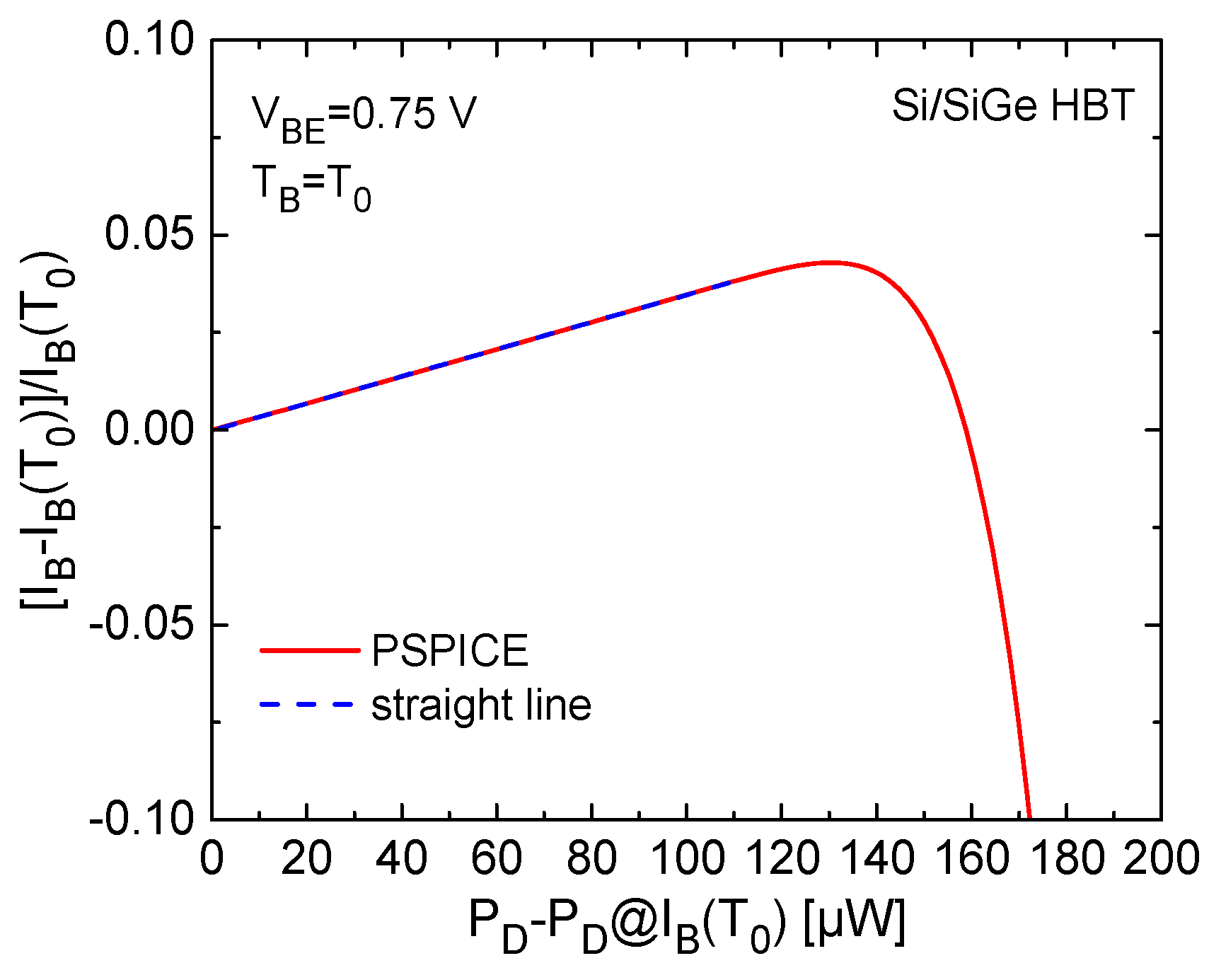
For the Si/SiGe HBT, the extraction was conducted at V B E = 0.75   V and T B = T 0 with the device mounted under common-emitter conditions. V C E = 0.55   V was selected as the voltage corresponding to the reference current I B T 0 = 82.5   nA . In this case, in the absence of any indication, the user might naturally choose E G = 1.12   eV on the RHS of (26), as this is the accepted bandgap of Si at T 0 . The extraction results corresponding to various V C E ranges for the evaluation of the slope of the linear behavior of I B I B T 0 I B T 0 against P D P D @ I B T 0 are listed in Table 4. In particular, the extraction of such a slope for V C E ranging from 0.55 to 1.2 V is illustrated in Figure 1. It is found that the extracted thermal resistances only slightly overestimate the reference value R T H 00 = 6855.8   K / W ; however, such results are most likely due to a compensation of the approximations leading to the simple (26), as it will be evident when testing the more accurate approach by Tran and co-workers [63], and therefore they should not be regarded as reliable. In addition, it must be emphasized that for Si/SiGe HBTs characterized by very high β F values, I B currents can be very small, and the overlapping measurement noise is likely to adversely affect the procedure.
In [63], Tran et al. improve the technique developed by Reisch as follows. A slightly simplified variant of their formula is given by
R T H = d d P D ln I B I B T 0 k T j 2 q 3 k T j q + V G V B E j η B = d d P D ln I B I B T 0 k T j 2 q 3 k T j q + E G q V B E j η B
where V G is generically referred to as the “bandgap voltage” and should more appropriately be replaced by V G E 0 Δ V G E , B G N ; in this respect, it is worth recalling that the authors explicitly account for Δ E G E , B G N when introducing the expressions for n i E T j , i.e., the square root of (13), and for the base current I B T j . Unfortunately, compared to the complete expression (23), the term R E B η B d I C d P D V T = R E B η B d I C d P D k T j q is disregarded. It is worth noting that (27) is an implicit equation with unknown R T H , as T j on the RHS is given by (1). Moreover, V B E j = V B E R E B I C where R E B is given by (11); therefore, this technique requires the simultaneous extraction of R T H , R B , and R E .
Concerning the impact of the parasitic resistances, the authors neglect R B , so that V B E j V B E R E I E and (12) becomes
I B = I B S T j exp V B E R E I E η B V T
Let us define I B , R f r e e as the resistance-free base current, given by
I B , R f r e e = I B S T j exp V B E η B V T
Dividing (29) by (28) gives
I B , R f r e e I B = exp R E I E η B V T
Taking the logarithm of both sides of (30),
η B V T ln I B , R f r e e I B = R E I E
Let us focus on the practical application of the procedure; since the original work [63] does not explicitly address all the implementation details, we present our plausible interpretation of the approach.
The simultaneous extraction of R E and R T H requires two independent measurements:
  • I C and I B as functions of V B E at a constant V C E to extract R E (for a known R T H );
  • I C and I B as functions of V C E at a constant V B E , with V C B spanning a range within which avalanche multiplication is negligible, to extract R T H (for a known R E ).
As an initial step, it is assumed that the first measurement gives rise to isothermal data. Consequently, (31) becomes
η B V T 0 ln I B , R f r e e T 0 I B = R E I E
where V T 0 = k T 0 q and
I B , R f r e e T 0 = I B S T 0 exp V B E η B V T 0
Parameters I B S T 0 and η B can be optimized by comparing (33) and the PSPICE I B V B E characteristic at T B = T 0 and low current levels. I E is calculated as I C + I B , the LHS of (32) is then plotted as a function of I E , and R E is determined as the slope of the curve. Subsequently, this first R E estimate is inserted into (27) to extract R T H . However, (27) is a local differential expression explicitly containing the junction temperature T j , which varies with the dissipated power P D according to (1); hence, R T H must be evaluated point-by-point against the swept V C E . Yet, the original paper [63] does not clarify the criterion for the choice of the single R T H value to be used for the subsequent step; we decided to evaluate an average R T H value within the V C E span where the extracted R T H vs. V C E behavior remains nearly linear, which means that the constant- V B E characteristic is not yet significantly distorted by self-heating. The average R T H value is subsequently used for the evaluation of T j through (1); T j is in turn exploited to determine I B S T j according to (14) and I B , R f r e e from (29). Consequently, an updated behavior of the LHS of (31) vs. I E is obtained, which allows for the extraction of an improved R E ; the improved R E is used to determine the average R T H from (27); this process is repeated until R E and the average R T H converge.
Such an iterative procedure was first applied to the InGaP/GaAs HBT. Unfortunately, the first step was found to be rather critical. While it is easy to optimize I B S T 0 = 3.61 × 10 26   A and η B = 1 . 033 , particular care should be taken in choosing V C E , as well as in defining the range of I E , for the evaluation of the slope of the LHS of (32) vs. I E . Selecting V C E = 1.5   V , this slope turned out to be negative, which is inconsistent with its interpretation as an emitter series resistance R E . This occurs because the self-heating produces a significant increase in I B , which outweighs the reduction caused by R E . Hence, the assigned V C E was lowered to 1 V. In this case, over low/medium I E values the slope was found to be positive (yet less positive than it would be in the presence of resistive effects only), but markedly dependent on the selected I E range, as shown in Table 5. From this table, it is evident that the extracted first-guess R E values are much lower than the actual emitter resistance embedded in the transistor model, i.e., 0.5 Ω. R E = 30   m Ω was selected as initial guess for the R T H evaluation through (27).
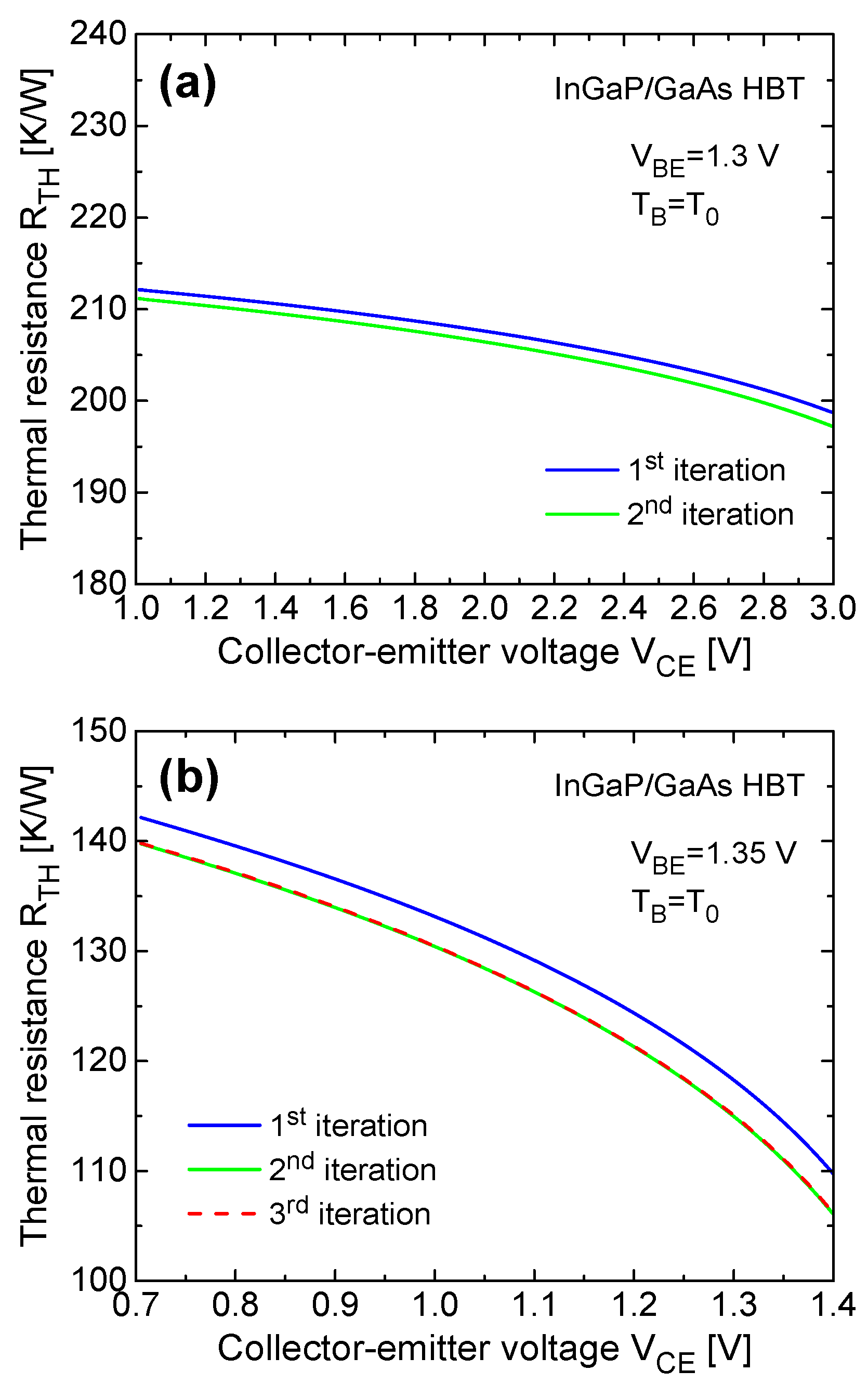
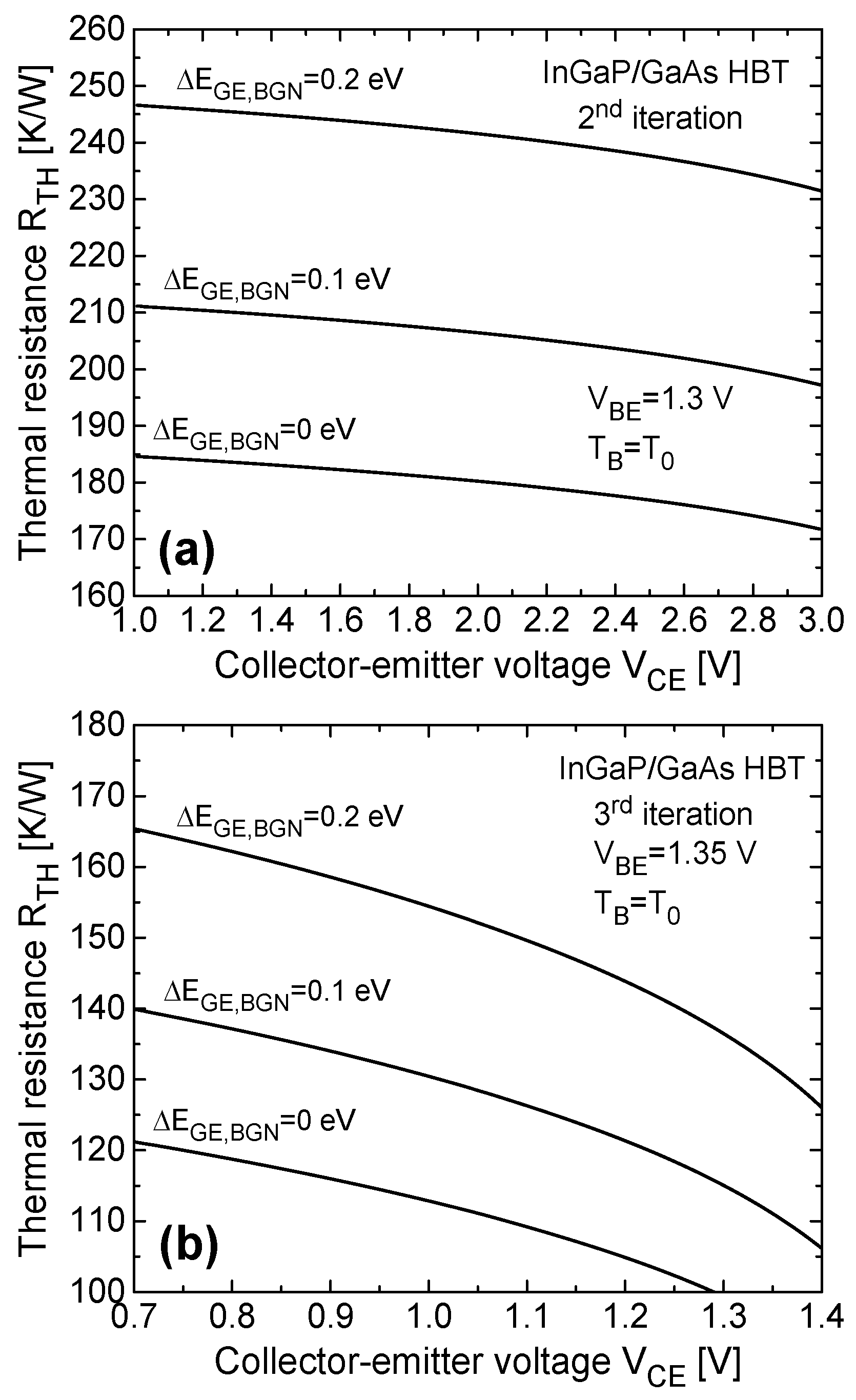
As in the Reisch procedure, the PSPICE simulation for R T H extraction was performed by sweeping V C E at V B E = 1.3   V and T B = T 0 . The minimum V C E value was assumed to be 1 V, at which I B T 0 = 47.89   µ A . Equation (27) with E G = E G E 0 Δ E G E , B G N = 1.98   eV 0 . 1   eV gave rise to the 1st iteration R T H V C E curve shown in Figure 2a; from this curve, an average R T H value of 210   K / W was arbitrarily chosen over the range where moderate self-heating arises, and then inserted into (31), where I B , R f r e e is given by (29), with I B S T j expressed by (14). From the slope of the LHS of (31) vs. I E , R E = 0.484   Ω was determined over the I E range 0.04 to 0.06 A, in close agreement with the actual value of 0.5 Ω. Subsequently, (27) yielded the 2nd iteration R T H V C E curve, also reported in Figure 2a, from which an average R T H value of 209   K / W was computed. Hence, the iterative process reached convergence.
The procedure was repeated by applying V B E = 1.35   V , T B = T 0 , using the same value of E G as above. The minimum V C E value was assumed to be 0.7 V, at which I B T 0 = 0.247   mA . Equation (27) led to the 1st iteration R T H V C E curve shown in Figure 2b; from this curve, an average R T H value of 140   K / W was estimated, and then fed into (31). From the slope of the LHS of (31) vs. I E , R E = 0.333   Ω was evaluated. Then (27) yielded the 2nd iteration R T H V C E curve in Figure 2b, from which an average R T H value of 137   K / W was computed. Then R E was determined to be 0.327 Ω, which was inserted into (27) and gave rise to the 3rd iteration R T H V C E characteristic. As this curve nearly overlaps the 2nd iteration one, the iterative procedure can be considered converged.
The impact of the BGN in the emitter was determined by also analyzing the cases Δ E G E , B G N = 0   eV and Δ E G E , B G N = 0.2   eV . Similar values of R E were obtained; unfortunately, it was found that (i) the average R T H is markedly sensitive to Δ E G E , B G N and (ii) it significantly underestimates the target R T H 00 = 460   K / W over the analyzed range of Δ E G E , B G N , as illustrated in Figure 3.
For the Si/SiGe HBT, I B S T 0 = 8.39 × 10 20   A and η B = 1 . 05 . Again, care is required in selecting V C E ; if the PSPICE I B V B E characteristic at V C E = 1   V is considered, the slope of the LHS of (32) vs. I E is found to be negative due to the significant self-heating occurring at medium V B E values. By contrast, considering the I B V B E curve at V C E = 0.6   V , the slope becomes positive. Again, the extracted initial estimate of R E was found to be significantly dependent on the selected I E range, as reported in Table 6. It is worth noting that the actual R E embedded in the transistor model amounts to 6 Ω.
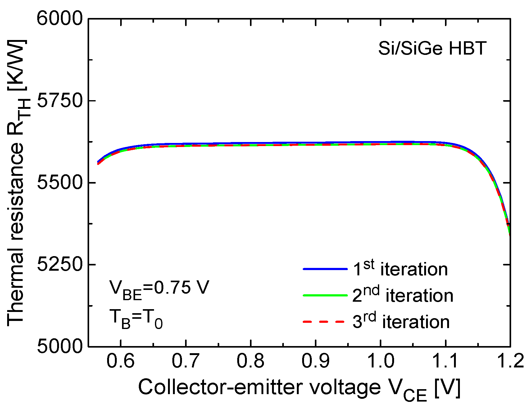
From a visual inspection of the values reported in Table 6, we selected R E = 2.7   Ω as an initial guess. The PSPICE simulation for the R T H extraction was executed by sweeping V C E at V B E = 0.75   V and T B = T 0 . The minimum V C E value was assumed to be 0.55 V, at which I B T 0 = 82.5   nA , as mentioned earlier. E G = E G E 0 Δ E G E , B G N = 1.21   eV 0 . 1   eV was chosen in (27), as 1.21 eV is the recommended value extrapolated to 0 K for Si. Using (27) with R E = 2.7   Ω , the 1st iteration R T H V C E curve was obtained, from which the average R T H = 5620   K / W was estimated and fed into (31); from the slope of the LHS of (31) vs. I E , it was obtained that R E = 6.34   Ω over the I E range from 2 to 6 mA, close to the actual value. In the 2nd iteration, the average R T H and R E were determined to be 5614 K/W and 6.33 Ω. Inputting R E = 6.33   Ω into (27), it was found that the 3rd iteration R T H V C E characteristic practically coincides with the 2nd iteration one, thereby indicating convergence of the iterative procedure. The R T H V C E characteristics corresponding to all the iterations are shown in Figure 4. Again, the average R T H value significantly underestimates R T H 00 .
The results confirm the findings obtained for the InGaP/GaAs HBT, which can be summarized as follows. Although the iterative procedure converges rapidly, the technique suffers from various limitations. First, (27) is only an approximation of the complete (23), since an R E B -dependent term is neglected. Second, this approach involves the estimation of a single representative R T H value from an R T H V C E curve originating from T j on the RHS of (27) without providing a clear criterion for its choice. Third, the method exhibits a pronounced sensitivity to the value of the emitter bandgap extrapolated to 0 K E G = E G E 0 Δ E G E , B G N to be inserted into (27); as this parameter is generally uncertain a priori, and thus unavailable to the user, the practical applicability and robustness of the extraction procedure are somewhat compromised.
Additional limitations deserve mention. Care should be taken when selecting the V C E to be applied for the initial R E guess, so as to avoid a negative slope of the LHS of (32) vs. I E , which further affects the robustness of the procedure. A practical difficulty–leading to higher inaccuracy–may arise in Si/SiGe HBTs because of the measurement noise affecting their extremely small base currents (it should be recalled that this noise is totally absent in the synthetic PSPICE data used in this work). Lastly, the technique is not conceived to extract nonlinear thermal effects, i.e., the influence of backside temperature T B and dissipated power P D on R T H .

4.2. Zweidinger et al. [62]

Similar to the thermometer-assisted method developed by Bovolon et al. [51] (also described in Part I [70]), this technique relies on a differential formulation. Neglecting resistive effects, and considering the bipolar transistor mounted in a common-emitter configuration, the collector current I C is a function of V B E , V C E , and T j , that is,
I C = I C V B E , V C E , T j
Consequently, under constant- V B E conditions, its total differential can be written as
d I C = 𝜕 I C 𝜕 V C E d V C E + 𝜕 I C 𝜕 T j d T j
I C varies with V C E at a given T j because of the Early effect, and 𝜕 I C 𝜕 V C E I C V A F , where V A F is the forward Early voltage; therefore,
d I C = I C V A F d V C E + 𝜕 I C 𝜕 T j d T j
where d T j can be due either to a small variation in the backside temperature d T B at a constant V C E   d V C E = 0 or to a variation d V C E at a constant T B   d T B = 0 . In the first case,
d I C d V C E = 0 = 𝜕 I C 𝜕 T j d T j d V C E = 0
while in the second
d I C d T B = 0 = I C V A F d V C E d T B = 0 + 𝜕 I C 𝜕 T j d T j d T B = 0
For a first-order analysis, P D , given by (2), can be approximated as V C E I C so that (1) reduces to
T j T B + R T H V C E I C
From (39), the variation in T j caused by a small variation d T B is
d T j d V C E = 0 = d T B d V C E = 0 + R T H V C E d I C d V C E = 0 = d T B d V C E = 0 + R T H V C E 𝜕 I C 𝜕 T j d T j d V C E = 0
whence
d T j d V C E = 0 = d T B d V C E = 0 1 R T H V C E 𝜕 I C 𝜕 T j
Moreover, from (39), the variation in T j due to a small variation d V C E is
d T j d T B = 0 R T H d I C d T B = 0 V C E + I C d V C E d T B = 0
which, exploiting (38), becomes
d T j d T B = 0 = R T H I C 1 + V C E V A F d V C E d T B = 0 + R T H V C E 𝜕 I C 𝜕 T j d T j d T B = 0
whence
d T j d T B = 0 = R T H I C 1 + V C E V A F d V C E d T B = 0 1 R T H V C E 𝜕 I C 𝜕 T j
Let us consider that the base current I B , in the absence of resistive effects, is a function of V B E and T j , that is,
I B = I B V B E , T j
Consequently, under constant- V B E conditions, its total differential can be written as
d I B = 𝜕 I B 𝜕 T j d T j
If d T j is induced by a small variation in the backside temperature d T B ,
d I B d V C E = 0 = 𝜕 I B 𝜕 T j d T j d V C E = 0
If d T j is induced by a small variation in the collector-emitter voltage d V C E ,
d I B d T B = 0 = 𝜕 I B 𝜕 T j d T j d T B = 0
Dividing (47) by (48) and making use of (41) and (44),
d I B d V C E = 0 d I B d T B = 0 = d T j d V C E = 0 d T j d T B = 0 = d T B d V C E = 0 R T H I C 1 + V C E V A F d V C E d T B = 0
from which
R T H = 1 I C 1 + V C E V A F d I B d V C E d T B = 0 d I B d T B d V C E = 0 = 1 I C 1 + V C E V A F I B V B E , V C E + d V C E , T B I B V B E , V C E , T B d V C E I B V B E , V C E , T B + d T B I B V B E , V C E , T B d T B
Equation (50) can be used for any bipolar transistor technology. Its adoption for conventional Si BJTs requires the preliminary knowledge of the Early voltage V A F ; in HBT technologies the Early effect is generally weak, so that 1 + V C E V A F 1 .
The technique can be practically applied by (i) measuring three characteristics at V C E , T B   , V C E + d V C E , T B   , and V C E , T B + d T B   by sweeping V B E , with V C B low enough to safely neglect the avalanche effect, (ii) identifying the three I B   values on the RHS of (50) at a chosen V B E , and (iii) using the I C value at V B E , V C E (nominal bias condition), and T B .
It is worth noting that, albeit not clarified in the original paper [62], the procedure could in principle be repeated at different T B values. Provided that the dissipated power P D is relatively low, this would allow obtaining the experimental R T H B 0 as a function of T B .
A major limitation of this technique concerns its inherently poor numerical robustness. The extracted R T H is highly sensitive to several user-defined quantities, including the selected bias point V B E , V C E at the assigned T B , the small increments d V C E and d T B employed for the numerical differentiation, as well as the interpolation procedure adopted to reconstruct the currents at that point. As these issues arise even when synthetic noiseless data are used, the robustness is expected to deteriorate further when this differential procedure is applied to actual experimental data; a similar conclusion is drawn in the review [69].
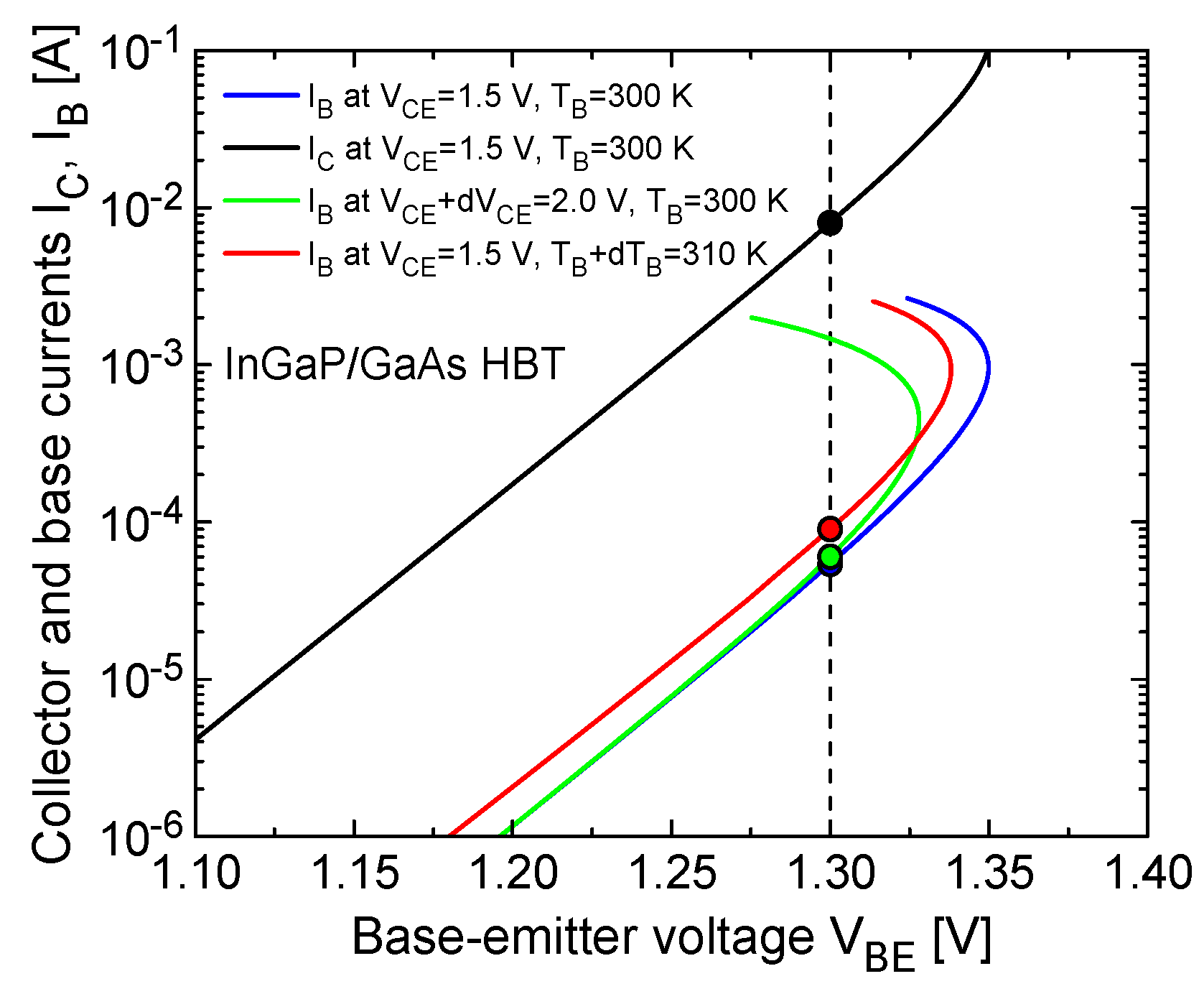
Let us first consider the InGaP/GaAs HBT under test at V C E = 1.5   V and T B = T 0 = 300   K . The increments d V C E and d T B were initially chosen to be 0.5 V and 10 K to ensure a practical compromise between sensitivity to potential measurement noise and accuracy of the differential evaluation. Selecting V B E = 1.3   V and performing an extremely fine shape-preserving interpolation to get I C V B E , V C E , T B , I B V B E , V C E , T B , I B V B E , V C E + d V C E , T B , and I B V B E , V C E , T B + d T B at the chosen bias point, (50) yielded R T H = 413.84   K / W , to be compared to R T H 00 = 460   K / W and to the reference value 464 K/W obtained from (7) by inputting T B = T 0 and the value of P D at the selected bias point. The application of the procedure is shown in Figure 5.
Repeating the extraction at the nearby operating points, namely, V B E = 1.28 , 1.29, and 1.31 V and retaining the same interpolation procedure to reconstruct the current values led to R T H = 385.17 , 396.27, 446.94 K/W, which reveals a perceptible sensitivity of the extraction outcome to V B E .
A step-size sensitivity investigation was also performed by repeating the whole analysis for different, experimentally reasonable, d V C E and d T B values.
Moreover, to assess the robustness of the method against finite current-measurement accuracy, the current values entering (50) were subsequently perturbed within assumed uncertainty bounds (±0.01 mA for I C   and ±0.1 µA for I B   ); this procedure allowed determining the worst-case uncertainty range, limited by the minimum and maximum R T H values extracted by the technique. This was initially done for each d V C E , d T B combination at V B E = 1.3   V ; then, an overall practical uncertainty range was defined as the envelope of the ranges obtained for V B E = 1.28 , 1.29, 1.3, and 1.31 V, representative of the interval of possible values that a practitioner may obtain when applying the technique to real-world experimental data. The results are summarized in Table 7.
The table clearly shows that the extracted R T H is highly sensitive to the selected increments d V C E , d T B and to the realistic uncertainties affecting the measured currents. This undesired behavior is an intrinsic consequence of the differential nature of the approach, which relies on finite differences between closely spaced current values. A key finding is that reducing d V C E improves the locality of the finite-difference approximation, but at the same time reduces the current differences, thereby amplifying the influence of the measurement uncertainty.
Overall, the results indicate that no unique combination of the bias point and finite increments can be regarded as optimal, which ultimately limits the practical reliability of the method.
The technique was also applied to the Si/SiGe HBT. Special care was required in selecting the operating conditions because of the low breakdown voltage. We chose V C E = 1   V , T B = T 0 = 300   K , d V C E = 0.2   V , d T B = 10   K . Assigning V B E = 0.8 , 0.81, 0.82, 0.83 V, and considering an accurate shape-preserving interpolation procedure for the evaluation of the currents, the extracted R T H values were found to be 5840, 5940, 6055, 6184 K/W to be compared with R T H 00 = 6855.8   K / W or to the values obtained from (7) by inputting T B = T 0 = 300   K and the actual value of P D at each V B E ; for example, at V B E = 0.8   V , (7) provides R T H = 6935   K / W . Considering the impact of the measurement accuracy for the values of I B and I C further widens the span of the extracted R T H ; more specifically, assuming the same relative current uncertainties as for the case of the InGaP/GaAs HBTs leads to an R T H worst-case uncertainty range of 3000–7000 K/W.

4.3. Williams and Tasker [64]

This technique can be viewed as an attempt to eliminate measurements at different backside temperatures. Unfortunately, the theoretical background and the practical procedure were somewhat cryptic in the original manuscript [64]; hence, the following derivation reflects our interpretation.
The general expression of the base current I B is given by (9), or, equivalently, by (12), which highlights the contribution of the aggregate parasitic resistance R E B . At low/medium current levels, the term R E B I C can be disregarded, and (12) becomes equal to I B , R f r e e given by (29), that is,
I B = I B , R f r e e = I B S T j exp V B E η B V T = I B S T j exp V B E η B k T j q
As discussed earlier, neglecting the temperature dependence of the hole diffusivity in the emitter and taking into account (13) for the dependence of the intrinsic concentration in the same region, I B S T j can be expressed by (14); Williams and Tasker rewrite (14) as
I B S T j = I B 0 exp q ϕ B k T j I B 0 exp ϕ B η B k T j q
i.e., they implicitly neglect the term T j T 0 3 , write q ϕ B , referred to as “barrier height at the base-emitter diode”, instead of E G E 0 Δ E G E , B G N , and probably define I B 0 as
I B 0 = I B S T 0 exp ϕ B k T 0 q I B S T 0 exp ϕ B η B k T 0 q
It is worth noting that the second, approximate equality in (52) is acceptable only if the ideality factor η B is sufficiently close to unity.
Substituting (52) into (51) yields
I B = I B 0 exp V B E ϕ B η B k T j q
whence
V B E = ϕ B η B k T j q ln I B 0 I B
Considering T B = T 0 in (1), the junction temperature T j can be expressed as T 0 + R T H P D , where R T H is assumed to be P D -independent, so that (55) becomes
V B E = ϕ B η B k T 0 q ln I B 0 I B η B k R T H P D q ln I B 0 I B
Concerning the practical application, Williams and Tasker propose to (i) measure a set of V B E V C E characteristics at different I B values; (ii) process the data to obtain the corresponding V B E P D curves; (iii) for each curve, find a straight line approximating the experimental V B E P D behavior; (iv) determine the slopes γ = d V B E d P D of such lines (with γ being necessarily negative for a bipolar transistor subject to self-heating), as well as their intercepts with the V B E axis at P D = 0   W , denoted by V B E P D = 0 . Starting from (56), it is possible to obtain that
ln I B = ln I B 0 ϕ B η B k T 0 q + V B E P D = 0 η B k T 0 q
and
ln I B = ln I B 0 γ η B k q R T H
from which
R T H = γ η B k q ln I B 0 I B
As the absolute slopes γ and the V B E P D = 0 intercepts are extracted at different base currents I B , two plots can be constructed with the available data, namely, ln I B vs. γ and ln I B vs. V B E P D = 0 ; I B 0 can be determined by extrapolating the first plot to γ = 0   V / W according to (58), whereas η B and ϕ B can be obtained from the slope and the extrapolation to V B E P D = 0 = 0   V (in particular, ϕ B is determined using I B 0 extracted in the former step) of the second, respectively, according to (57). Lastly, substituting I B 0 and η B into (59),   R T H can be evaluated at each I B .
It should be noted that, strictly speaking,   R T H is derived from a V B E P D curve where I B is forced; on the other hand, this technique makes use of the temperature dependence of I B (like the techniques proposed in [61,63,65]). For this reason, this method was included in the category of techniques exploiting the base current.
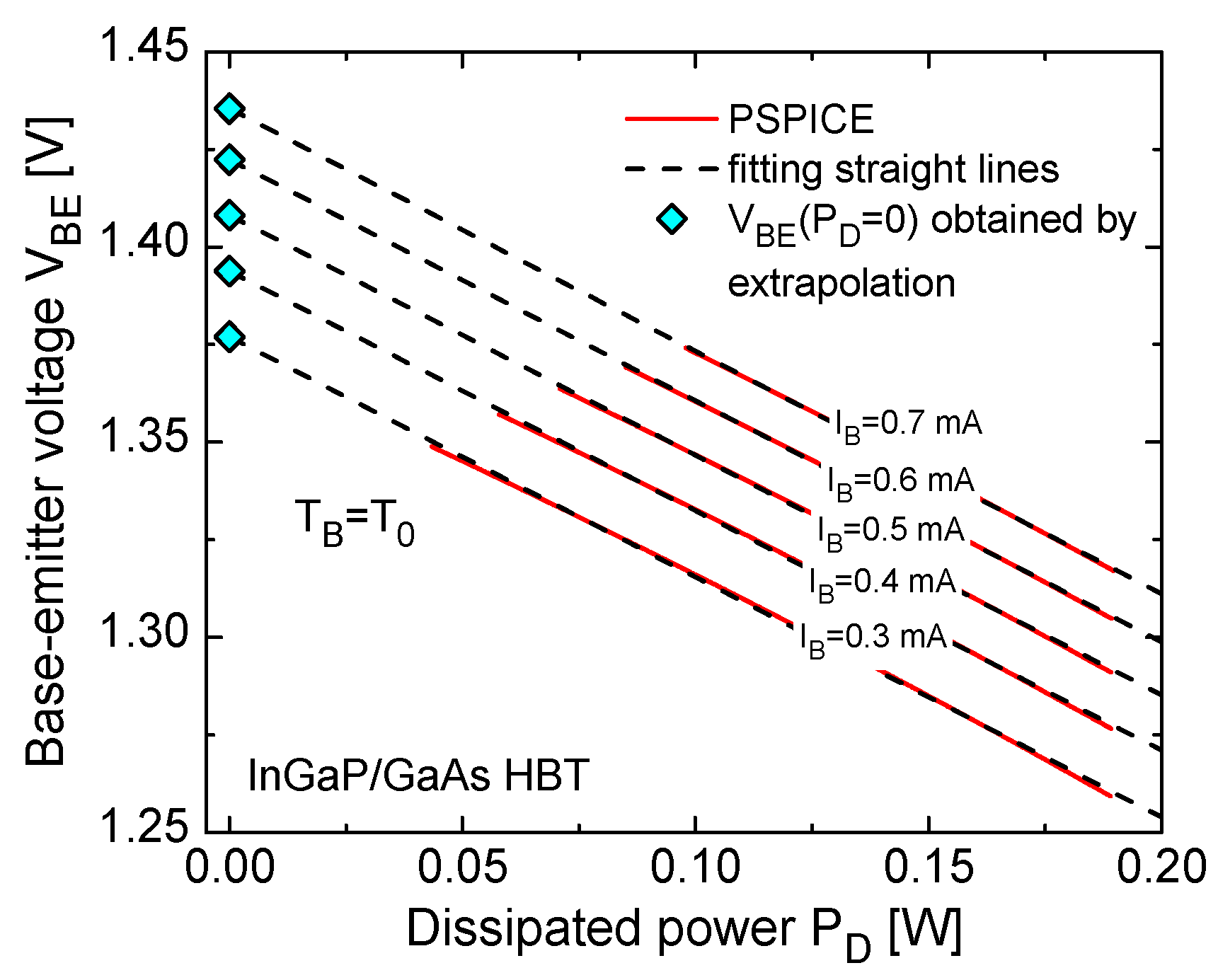
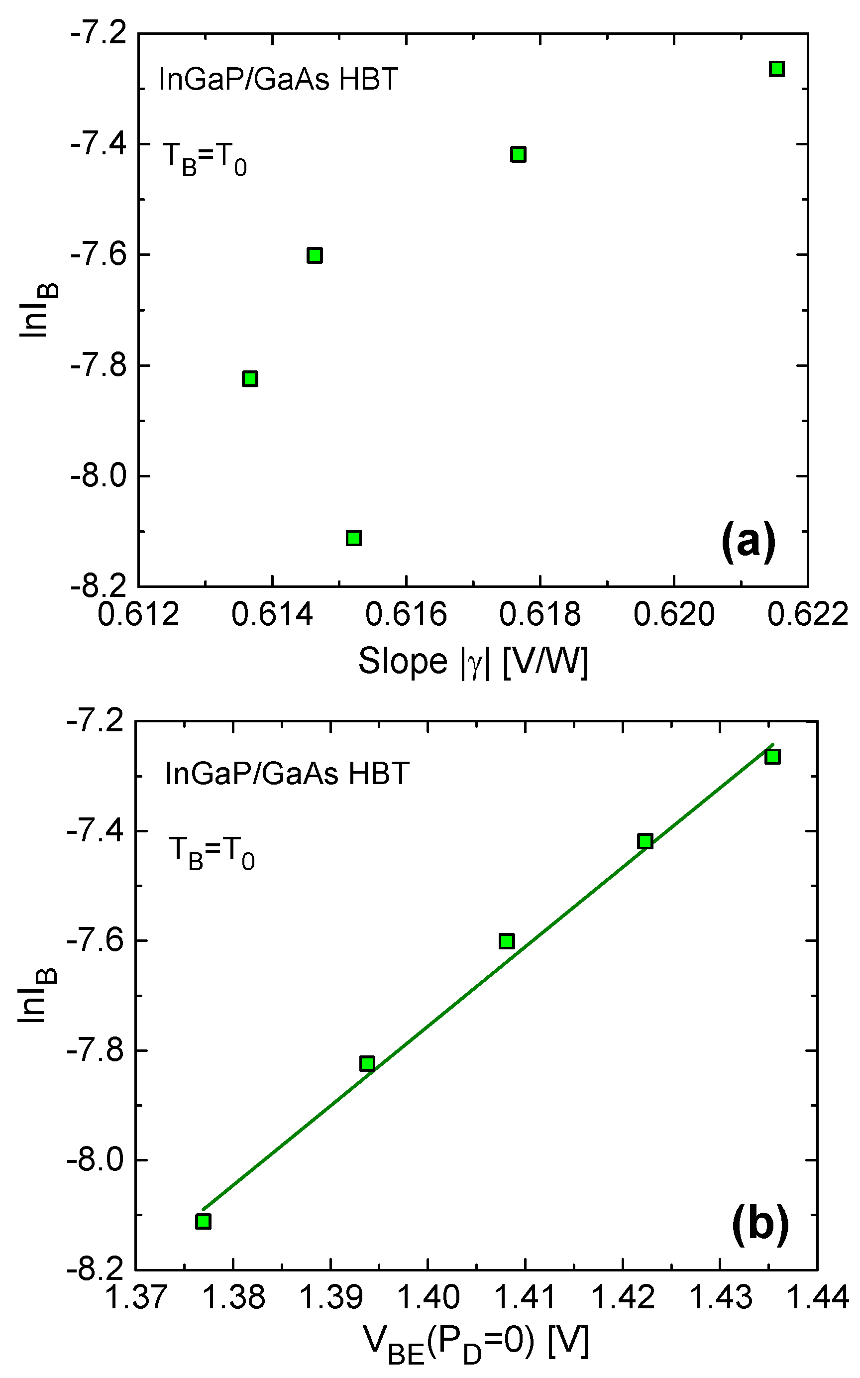
The approach was applied to the InGaP/GaAs HBT under test. The V B E V C E curves were simulated through PSPICE at T B = T 0 for I B values spanning the 0.3–0.7 mA range with a 0.1 mA step, and the corresponding V B E P D characteristics were determined. Straight lines were fitted to the linear portion of these curves where the HBT operates under forward active mode, which allowed obtaining the slopes γ and the extrapolated intercepts V B E P D = 0 at each I B , as shown in Figure 6. Subsequently, the plots reporting ln I B vs. γ (Figure 7a) and ln I B vs. V B E P D = 0 (Figure 7b) were constructed; from the first, I B 0 = 1.414 × 10 25   A , while from the second, η B = 2.67 and ϕ B 2   V (using the extracted I B 0 ). Unfortunately, all such values are non-physical: q ϕ B is the positive bandgap E G E 0 Δ E G E , B G N ; η B is expected to be close to unity (values I B S T 0 = 3.61 × 10 26   A and η B = 1.033 were independently extracted in Section 4.1 from a synthetic PSPICE I B V B E characteristic at T B = T 0 ); using I B S T 0 = 3.61 × 10 26   A , η B = 1.033 , and a reasonable value for ϕ B , (53) would provide an I B 0 many orders of magnitude higher than 1.414 × 10 25   A ; moreover, η B = 2.67 makes the approximation in (52) unacceptable. Substituting I B 0 = 1.414 × 10 25   A and η B = 2.67 into (59) gives rise to a negative, almost I B -independent, R T H value of approximately 54   K / W .
The failure of the approach can be explained as follows. Although the individual constant- I B   V B E P D characteristics exhibit excellent linearity, the synthetic PSPICE data do not satisfy the assumptions of the technique. In particular, as shown in Figure 7a, γ varies non-monotonically with increasing I B primarily due to the R T H intrinsic dependence on P D ; hence, the extraction of I B 0 , which requires a remote extrapolation of the ln I B vs. γ data to γ = 0   V / W , is severely ill-conditioned and leads to an I B 0 much lower than physically reasonable values. Furthermore, the extracted η B is unreliable, since it is inferred from the slope of the ln I B vs. V B E P D = 0 data, whose abscissas were obtained by extrapolation, i.e., by assuming (56) to be valid down to very low dissipated powers (ideally, for P D 0 ). Lastly, even when the R E B I C voltage drop is relatively small, neglecting it may appreciably alter the fitted slopes and intercepts, thereby further compromising the extraction of I B 0 and η B ; the original study itself [64] emphasized the strong sensitivity to the resistive drop.
In light of the above considerations, the technique was not applied to the Si/SiGe HBT.

4.4. Pawlak et al. [65]

Let us refer to (9) or, equivalently, to (12), which, neglecting the parasitic base resistance R B , reduces to (28), where R E is assumed to be temperature-insensitive. If I B measurements are performed by sweeping V B E under constant- V C E conditions at various backside temperatures T B , for current levels sufficiently low to safely neglect self-heating ( T j T B ) and the voltage drop over R E , (28) turns into
I B = I B , R f r e e T B = I B S T B exp V B E η B k T B q
This procedure allows the concurrent extraction of the I B S vs. T B behavior and the ideality factor η B . Although not explicitly indicated in [65], a formulation should be used to describe the I B S vs. T B dependence. We decided to extend the original procedure by adopting the physics-based model
I B S T B = I B S T 0 T B T 0 3 exp E G E 0 Δ E G E , B G N k 1 T B 1 T 0
obtained by replacing T j with T B in (14). By comparing (61) and the I B S vs. T B data collected in the previous step, I B S T 0 and the bandgap E G E 0 Δ E G E , B G N can be optimized.
Then, Pawlak et al. state that in a first-order approximation, P D V C E R E I E I C so that
T j T 0 = R T H V C E R E I E I C
The procedure requires a measurement under constant- I C conditions by sweeping V C E at T B = T 0 . As explained in [65], if the device is mounted under common-emitter conditions, V C E is swept and V B E is regulated at each V C E value until the chosen I C is obtained, which however makes the measurement cumbersome. If the emitter terminal is available (not connected to ground), it is easier to perform a common-base constant- I E measurement by sweeping V C B , thus getting V C E as V C B + V B E , where V B E is measured. Feeding (28), where I B S T j is given by (14), with a trial emitter resistance value R E , I B and with the measured I B and V B E data, it is possible to obtain T j T 0 as a function of V C E . Subsequently, making a linear fit of the T j T 0 vs. V C E behavior, and extrapolating the intersection with the V C E axis at T j T 0 = 0   K , a V C E 0 is found, which from (62) is equal to
V C E 0 = R E I E
From (63), it is possible to determine a zero-crossing emitter resistance given by R E , V C E 0 = V C E 0 I E . Then, R E , I B is automatically updated through a bisection or Newton algorithm, the new T j T 0 vs. V C E behavior is obtained, leading to another R E , V C E 0 value, until the consistency equation R E , V C E 0 = R E , I B is satisfied. This implies that the procedure has reached convergence, thus providing the extracted R E and the final T j T 0 vs. V C E behavior. Lastly, the thermal resistance R T H can be easily determined from the slope of this curve, which, according to (62), is equal to R T H I C .
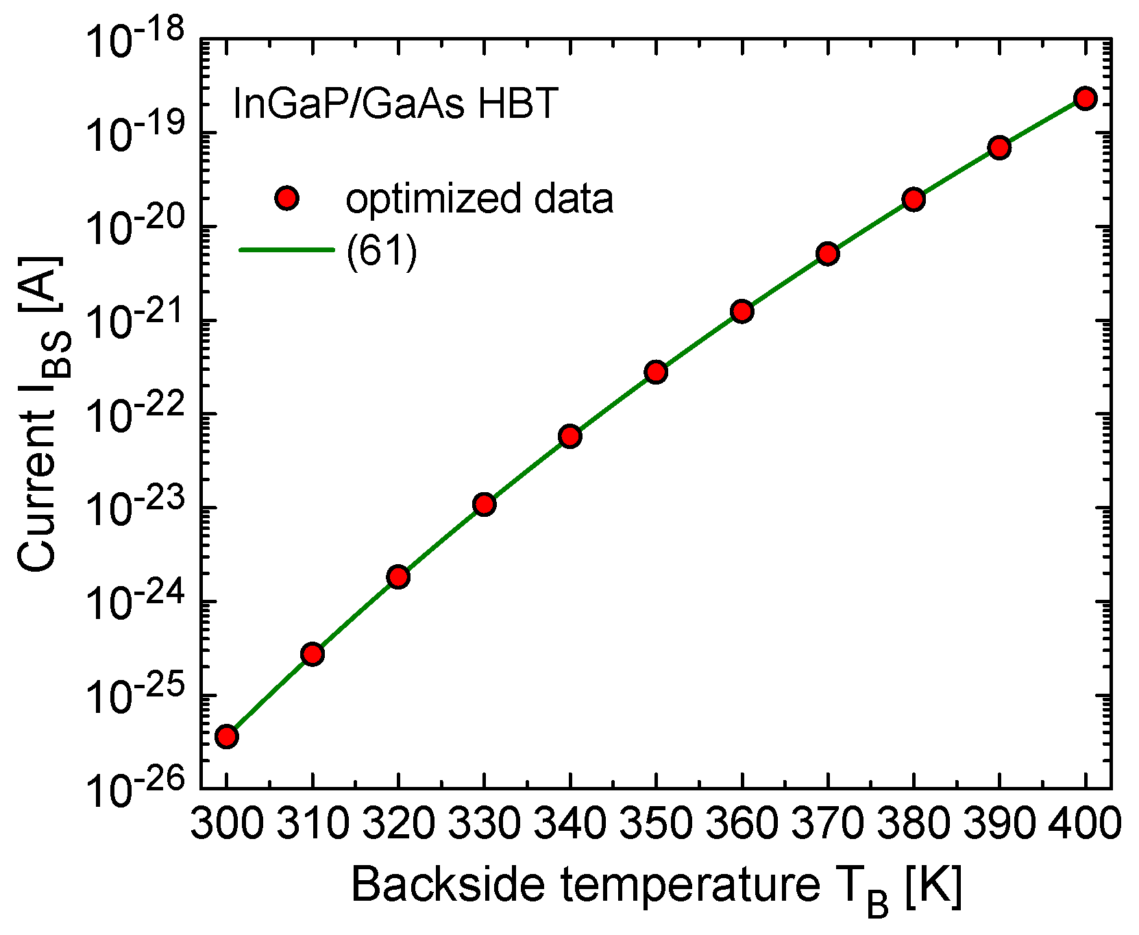
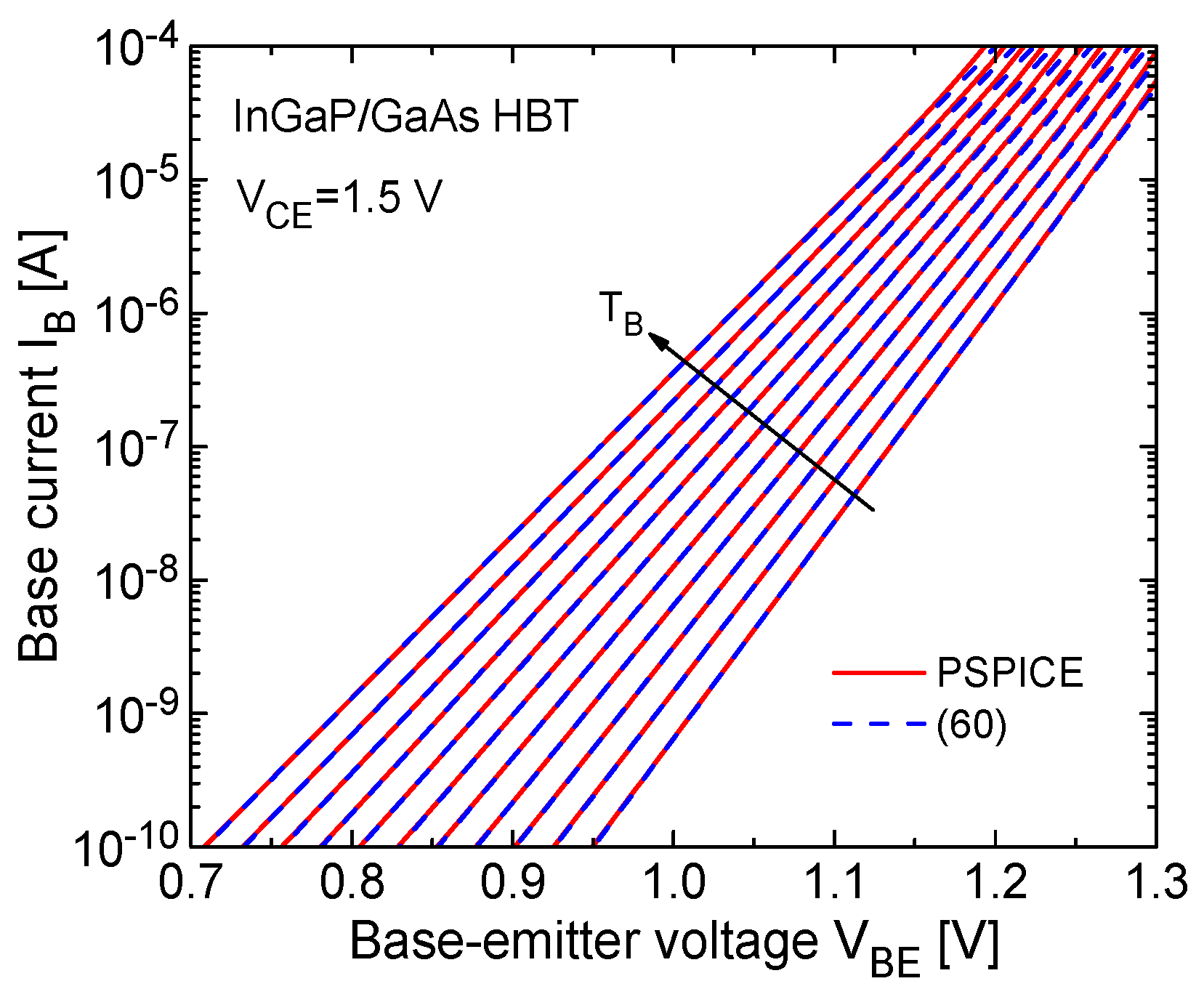
Figure 8 shows the I B V B E characteristics of the InGaP/GaAs HBT generated by PSPICE at V C E = 1.5   V and T B spanning the range 300–400 K with a 10 K step. These curves were compared with (60) to extract the current I B S at each T B and the ideality factor η B , which was again found to be 1.033.
Then, from the comparison between the resulting I B S vs. T B data and (61), the bandgap E G E 0 Δ E G E , B G N was calibrated to be 1.534 eV. This step is represented in Figure 9.
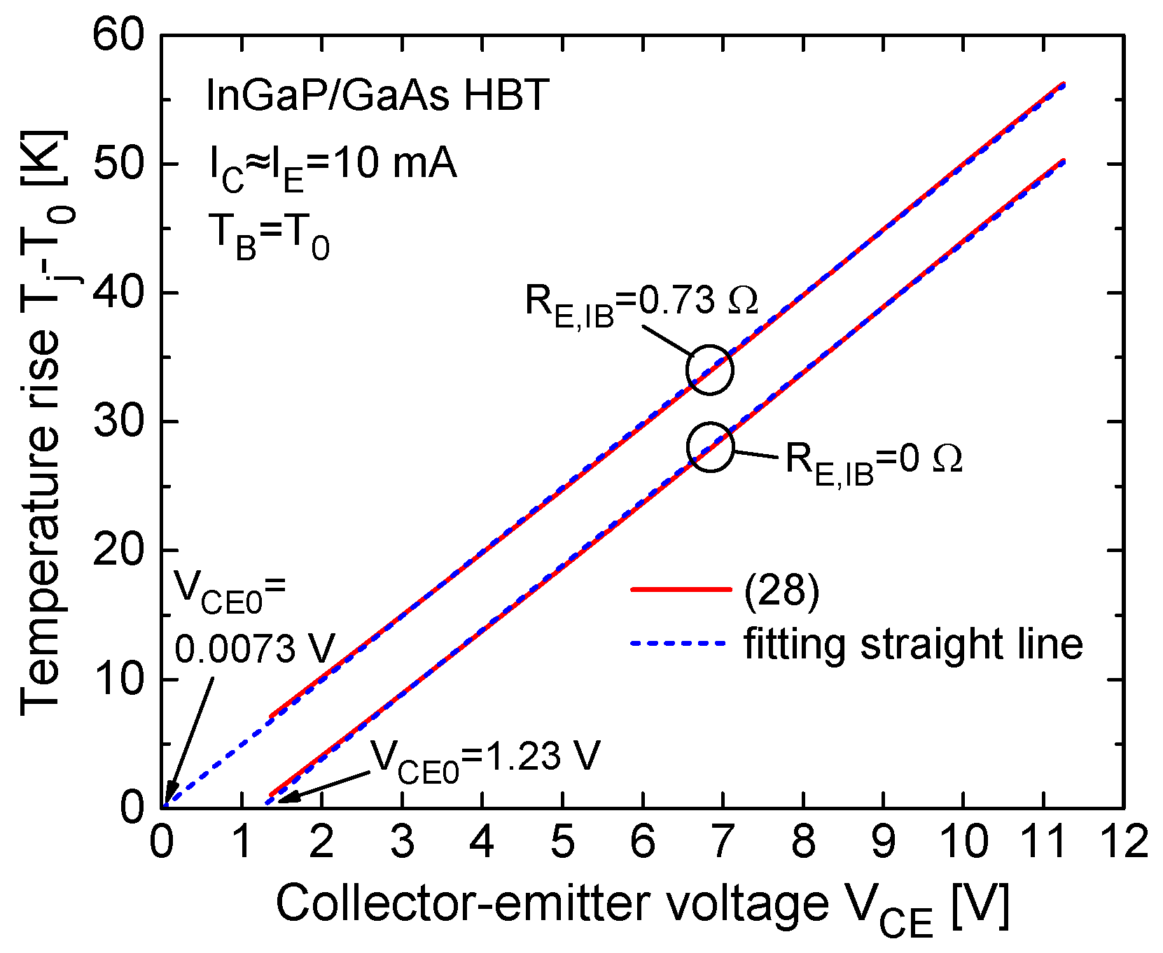
A PSPICE simulation of the device was then carried out under common-base conditions at I E = 10   mA by sweeping V C B . By initially assuming R E , I B = 0   Ω , from (28) the temperature rise T j T 0 was determined as a function of V C E , as shown in Figure 10. Following the procedure outlined above, it was found that V C E 0 = 1.23   V , from which R E , V C E 0 = V C E 0 I E = 123   Ω . After a few Newton-based iterations, the algorithm converged to R E = 0.73   Ω and R T H = 502.4   K / W , which overestimate by 46% and 9% the reference values R E = 0.5   Ω and R T H 00 = 460   K / W embedded in the transistor model. Figure 10 also reports the final T j T 0 vs. V C E behavior, along with the best-fit straight line and the zero-crossing V C E 0 = 0.0073   V leading to R E , V C E 0 = R E , I B = 0.73   Ω . The above discrepancies can be ascribed to (62), where the dissipated power is implicitly assumed to be given by P D = V C E R E I E I C , thus allowing the linear extrapolation of T j T 0 vs. V C E to vanish at V C E 0 = R E I E . However, (62) is questionable, since the power dissipated in a transistor must coincide with the total electrical power delivered to it through its external terminals (power balance dictated by energy conservation). In simple words, also the Joule loss R E I E 2 contributes to the self-heating and cannot be excluded from the dissipated power budget. For the sake of clarity, it must be noted that (62) constitutes the mathematical foundation for the entire algorithm: considering the physically consistent (2) or the approximate P D V C E I C makes the R E extraction unviable, and the whole procedure not self-contained.
Let us now consider the Si/SiGe HBT under test. By applying (60) to the I B V B E synthetic PSPICE characteristics at V C E = 1.0   V and various T B , the ideality factor was again found to be 1.05, and the I B S vs. T B data were available. Subsequently, by comparing such data with (61), the bandgap E G E 0 Δ E G E , B G N was optimized to be 1.024 eV. A PSPICE simulation of the transistor was then executed under common-base conditions at I E = 1   mA by sweeping V C B . By applying the Newton-based iterative procedure described earlier, it was found that R E = 6.473   Ω and R T H = 7246.8   K / W , with errors of 7.9% and 5.7% with respect to R E = 6   Ω and R T H 00 = 6855.8   K / W embedded in the transistor model.

5. Analysis of the Experimental RTH Extraction Technique of Menozzi et al.

The technique developed by Menozzi et al. [66] is conceived to allow the experimental extraction of R T H as a function of T B and P D based on a couple of assumptions. The method requires the common-emitter measurements of various (five to seven can be enough [66]) I C V C E characteristics at an assigned base current I B for various T B values, the lowest of which is referred to as T B 0 . Let us denote by V C E 0 the lowest V C E applied for the sweep of the entire family of curves ensuring that the bipolar transistor operates in forward active mode, and by I C 00 the collector current at the reference point defined by V C E = V C E 0 and T B = T B 0 . Lastly, let us call P D 0 the power dissipated at the starting point of all characteristics, i.e., at V C E = V C E 0 ; clearly, P D 0 depends on T B (in HBTs, it reduces with increasing T B due to the negative temperature coefficient of the common-emitter current gain β F ) and can be more effectively denoted by P D 0 T B .
The first assumption of the method is that, for any assigned T B , R T H T B , P D is a linearly increasing function of P D , that is,
R T H T B , P D = R T H T B , P D 0 T B + A T B P D P D 0 T B
where the slope A is a function of the applied T B and is expected to be positive.
The second assumption is that the collector current I C linearly decreases with T j (regardless of the mechanism responsible for the increase in T j ) at a given I B . This can be expressed as
I C T j = I C 00 1 κ T j T j 00
where κ > 0   K - 1 and T j 00 is the lowest junction temperature, i.e., the one corresponding to V C E 0 and T B 0 :
T j 00 = T B 0 + R T H T B 0 , P D 00 P D 00
Here, P D 00 denotes P D 0 T B 0 , which, by resorting to the approximation P D V C E I C , is given by V C E 0 I C 00 . Obviously, the assumption (65) can only be justified for HBTs due to the negative temperature coefficient of β F . Let us subtract (66) from (3):
T j T j 00 = T B T B 0 + R T H T B , P D P D R T H T B 0 , P D 00 P D 00
By making use of (64),
T j T j 00 = T B T B 0 + R T H T B , P D 0 T B + A T B P D P D 0 T B P D R T H T B 0 , P D 00 P D 00
Substituting the RHS of (68) into (65), we obtain
I C T B , P D = a 2 T B P D 2 + a 1 T B P D + a 0 T B
with
a 0 T B = I C 00 1 κ T B T B 0 R T H T B 0 , P D 00 P D 00 = B T B + C
representing the collector current extrapolated to P D = 0   W , and
a 1 T B = I C 00 κ R T H T B , P D 0 T B A T B P D 0 T B
a 2 T B = I C 00 κ A T B
Hence, I C is expressed as a function of T B and P D at any point of the measured curves.
First, the constant- I B   I C P D characteristics associated with the measured I C V C E ones are determined by a simple elaboration of the data. Then, the values of coefficients a 0 , a 1 , a 2 favoring the best agreement between the experimental I C P D curves and (69) are found for each T B , so that the three a 0 T B , a 1 T B , and a 2 T B characteristics are available. By comparing the a 0 T B curve and (70), parameters B and C can be calibrated. Consequently, κ can be evaluated as
κ = B I C 00
and the lowest thermal resistance R T H T B 0 , P D 00 as
R T H T B 0 , P D 00 = C I C 00 κ T B 0 1 κ P D 00
From (72), A T B can be obtained for each T B as
A T B = a 2 T B I C 00 κ
As a result, from (71), R T H T B , P D 0 T B can be determined at each T B as
R T H T B , P D 0 T B = A T B P D 0 T B a 1 T B I C 00 κ
Once A T B and R T H T B , P D 0 T B are known, the linear R T H vs. P D increase at each T B as given by (64) is achieved.
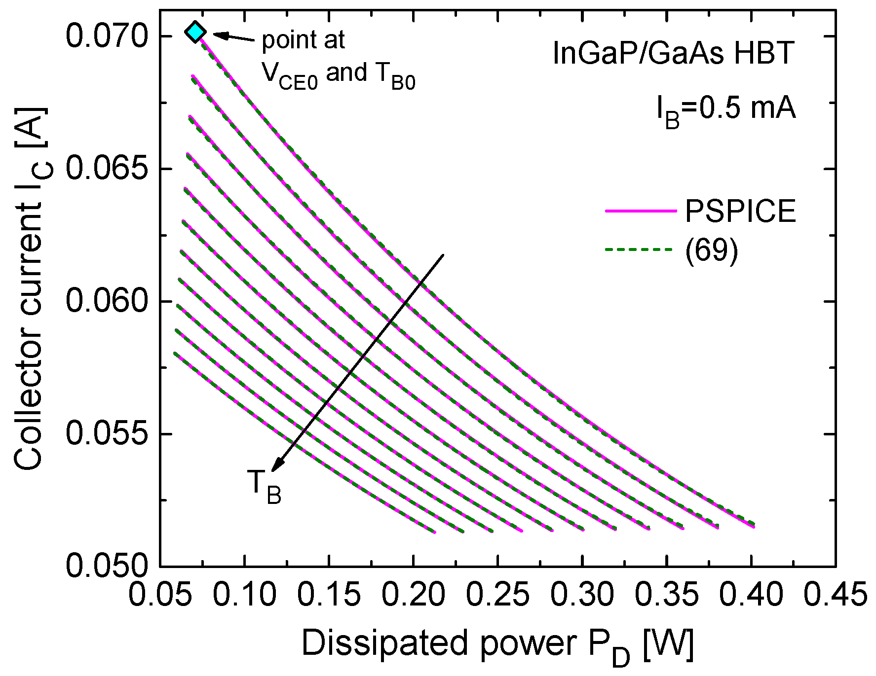
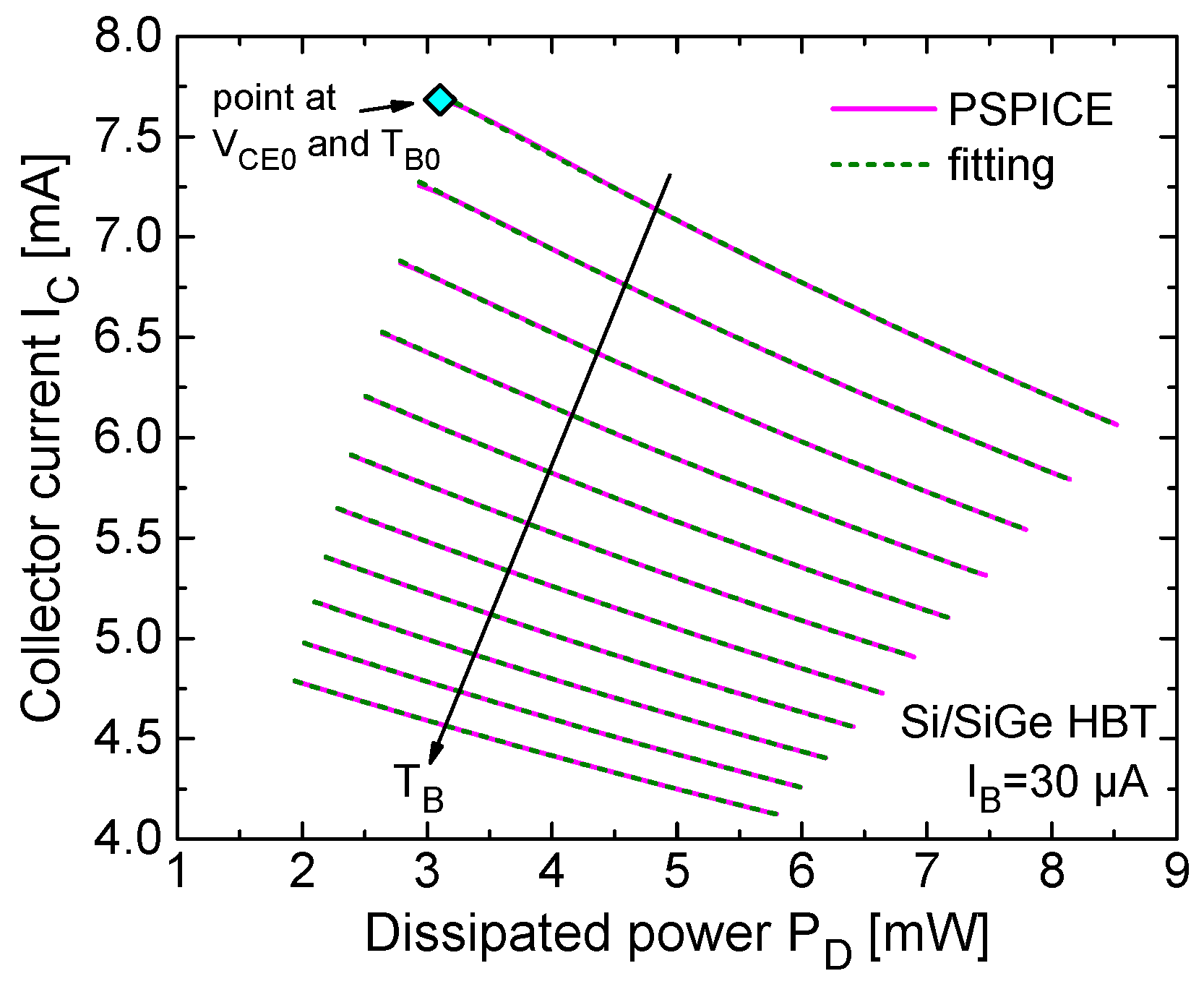
The technique was first applied to the InGaP/GaAs HBT. The I C V C E characteristics were simulated by PSPICE from V C E = V C E 0 = 1   V at a base current I B = 0.5   mA and varying T B from T B 0 = T 0 = 300   K to 400 K with a 10 K step. Figure 11 shows the corresponding I C P D curves alongside those obtained from (69) after optimizing coefficients a 0 , a 1 , a 2 at each T B .
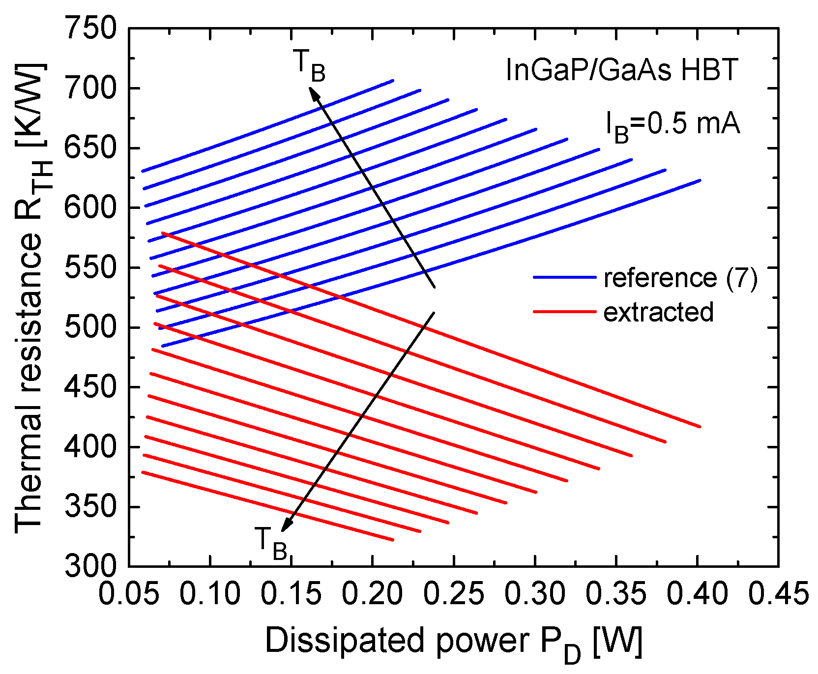
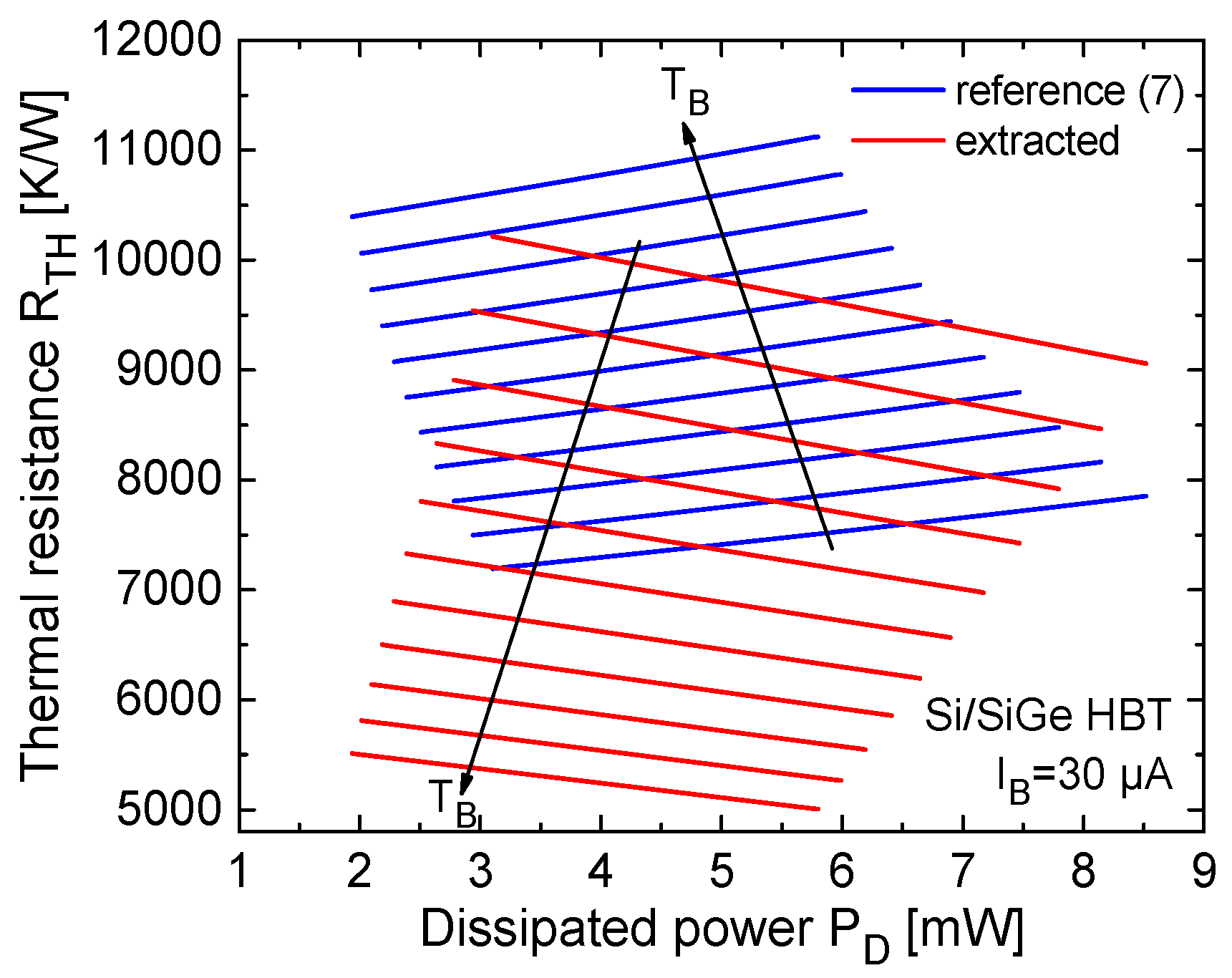
The thermal resistance R T H as a function of P D at various T B , obtained with the extraction technique, is shown in Figure 12, which also reports the target behavior computed from (7) with R T H 00 = 460   K / W and α = 0.95 . Unfortunately, the method produces rather inaccurate results: R T H decreases with increasing P D for an assigned T B (due to an extracted A T B < 0   K / W 2 ) and with increasing T B for a given P D , both trends being physically unreasonable. Moreover, the R T H T B 0 , P D 00 value obtained from (74), i.e., 476.8 K/W, does not coincide with the value computed from (64) at T B 0 and P D 00 , i.e., 578.9 K/W.
The inaccuracy of the technique is mainly ascribable to the assumption of linear dependence of I C on T j given by (65). Such an assumption is questionable for the following reason. Under forward active mode, at a constant I B , the collector current is given by I C T j = β F T j I B ; in HBTs, regardless of the selected technology, β F T j reduces with T j according to the well-known exponential law [70,81,82,83,84,85,86]
β F T j = β F T 0 exp Δ E G E B k 1 T j 1 T 0 = β F T 0 exp E G E E G B k 1 T j 1 T 0
where E G E and E G B ( E G E > E G B ) are the bandgaps in emitter and base, respectively. Assumption (65) is also criticized in [69], where synthetic I C vs. T j data are reported. Equation (77) leads to constant- T B  convex (curving upward) I C P D characteristics (e.g., [87]), and thus to positive coefficients a 2 at all backside temperatures T B that imply A T B < 0   K / W 2 , whereas the technique requires negative coefficients a 2 in order to obtain A T B > 0   K / W 2 and then an R T H T B , P D increasing with P D . The inconsistency of (65) also results in an R T H T B , P D reduction with T B and a difference between two quantities that should in principle coincide, namely, R T H T B 0 , P D 00 as given (i) by (74) and (ii) by inputting T B = T B 0 and P D = P D 00 into (64).
This finding was corroborated by the following analysis. In the transistor model implemented in PSPICE [70] we replaced formulation (77) with the simple linear law
β F T j = β F T 0 1 ξ β T j T 0
where ξ β > 0   K 1 . The constant- I B   I C V C E curves were again simulated by PSPICE and processed; in this case, the associated I C P D characteristics are concave (curving downward), coefficients a 2 are negative, which implies that A T B > 0   K / W 2 , and the technique predicts fairly well the reference R T H T B , P D behavior given by (7).
We are aware that Menozzi et al. showed a reasonable outcome of their procedure applied to characteristics measured on a 3 × 30 µm2 single-finger InGaP/GaAs HBT [66], that is, the resulting R T H T B , P D increases with both T B and P D , although the accuracy of the values could not be assessed. However, this was dictated by concave I C P D curves compatible with the underlying assumption of I C (and thus β F ) linearly decreasing with T j , which is theoretically inconsistent. One possible explanation for such a concave experimental I C P D behavior in [66] might be an uneven current density distribution over the emitter, which exacerbates the ET feedback and gives rise to a shape distortion of the I C V C E characteristics apparently due to a linear β F reduction with T j . In other words, it is likely that the technique does not provide inconsistent outcomes since the collector current measured at the device terminal reflects not only the intrinsic current gain of the transistor, described by the widely accepted (77), but also the distribution of the emitter current density.
Concerning the Si/SiGe HBT, the I C V C E characteristics were simulated by PSPICE from V C E = V C E 0 = 0.4   V to 1.4 V; such a low upper boundary was necessary to prevent a significant avalanche effect ( B V C E O = 1.6   V , as reported in Table 2), which would have adversely affected the extraction. A base current I B = 30   µ A was applied.
Figure 13 depicts the I C P D curves together with those obtained from (69) through optimization of coefficients a 0 , a 1 , a 2 at each T B , while Figure 14 illustrates R T H as a function of P D at various T B , as determined by the technique, and the reference behavior given by (7) with R T H 00 = 6855.8   K / W and α = 1.333 .
Unfortunately, the same inconsistencies observed for the InGaP/GaAs HBT were also found for the Si/SiGe HBT. In particular, the technique yields positive values of a 2 , A T B < 0   K / W 2 , an R T H T B , P D reducing with increasing T B at a given P D , and a significant discrepancy between the R T H T B 0 , P D 00 value obtained from (74), i.e., 7693.7 K/W, and that computed from (64) at T B 0 and P D 00 , i.e., 10,215.1 K/W. These physically meaningless results are again dictated by the assumption (65).
The present analysis based on synthetic data indicates that the technique proposed by Menozzi et al. [66] does not seem to be sufficiently robust for general-purpose R T H extraction, as the underlying assumption of a linear temperature dependence of I C does not reflect the theoretical constant- I B ET behavior of an HBT operated under a uniform distribution of emitter current density, and may yield inaccurate and physically inconsistent trends. Conversely, the technique can in principle provide an acceptable outcome when the shape of the experimental I C V C E characteristics leads to concave I C P D curves, which however are not consistent with (77). Consequently, the procedure seems to provide reasonable results only when the device deviates from the theoretically expected intrinsic ET behavior leading to convex I C P D curves.

6. Comparative Assessment and Practical Guidelines

This paper completes a three-part critical review of experimental techniques for extracting the self-heating thermal resistance of bipolar transistors from indirect DC current/voltage measurements at various backside temperatures. Throughout the trilogy, the original methods have been rederived within a unified theoretical framework and assessed by applying them to synthetic (and noiseless) ET characteristics generated through circuit simulations of transistor models embedding a known reference/target thermal resistance formulation. This controlled framework provides a best-case benchmark of the intrinsic accuracy and numerical robustness of each extraction procedure, as it isolates method-related issues from experimental uncertainties. Accordingly, good agreement with the reference thermal resistance should be regarded as a necessary, but not sufficient, condition for satisfactory experimental performance.
An InGaP/GaAs HBT and a Si/SiGe HBT were chosen as representative case studies, the latter technology being more critical than the first, as it is affected by avalanche multiplication (jeopardizing the extraction accuracy) at relatively low collector-base voltages.
Part I showed that thermometer-based techniques generally provide the most favorable compromise among theoretical soundness, experimental simplicity, numerical robustness, and accuracy, provided that the thermometer (the relation between the base-emitter voltage V B E and the junction temperature T j ) is carefully calibrated under sufficiently low-power conditions. Most thermometer-assisted techniques (Dawson et al., Rieh et al., Vanhoucke et al., d’Alessandro et al.) were found to be fairly accurate for the determination of the R T H 00 (the low-power thermal resistance at T B = T 0 = 300   K ) of the HBTs under test, for which the Early effect is negligible. Among the thermometer-based methods, the procedure proposed by Yeats deserves special attention because it enables a straightforward and accurate determination of nonlinear thermal effects, i.e., the R T H dependence on T B and P D . However, since this technique directly converts the thermometer into T j , its experimental performance is expected to be more sensitive to the V B E measurement accuracy than the other two-step procedures. The differential technique developed by Bovolon et al. can also be used to assess the impact of nonlinear thermal effects; unfortunately, it lacks robustness and fails to describe the nonlinear self-heating effect.
Techniques based on the identification of intersection points were conceived with the aim of getting rid of errors related to the thermometer evaluation. However, Part II demonstrated that eliminating the thermometer does not automatically improve the extraction accuracy. Most intersection-point methods suffer from severe approximations or even theoretical inconsistencies. Moreover, all of them are particularly sensitive to the numerical identification of the intersections; such an issue is expected to be further exacerbated by using actual experimental data due to the unavoidable measurement noise. Notably, a refined implementation of the technique developed by Huszka et al., relying on true intersection points, substantially improves the results and allows for the complete description of nonlinear thermal effects, thereby representing the most effective non-thermometer-based approach examined in this trilogy; on the other hand, this updated procedure is quite challenging to apply, as it requires an extensive measurement campaign, careful interpolation, and proper optimization routines.
Part III demonstrated that techniques exploiting the base current generally benefit from relatively simple measurement setups, although their practical performance is strongly method-dependent. The method proposed by Reisch and its improved variant conceived by Tran et al. (the latter aimed at extracting both R T H and the parasitic emitter resistance R E ) strongly depend on the emitter bandgap extrapolated to 0 K, which is generally unknown to the user; additionally, they are affected by simplifying assumptions that limit their extraction accuracy. The differential approach of Zweidinger et al. is highly sensitive to the selected bias point and the small increments in V C E and T B , besides being impacted by the current-measurement uncertainty at that bias point. The algorithm proposed by Williams and Tasker relies on two remote extrapolations. Although this procedure formally allows determining all the relevant I B parameters and the R T H , the extraction is severely ill-conditioned, ultimately leading to non-physical values for all the extracted quantities, including R T H . The procedure proposed by Pawlak et al. is designed to extract simultaneously R E and R T H by solving a nonlinear consistency condition between the trial value of an input R E used to determine the temperature rise and an output R E inferred with an extrapolation procedure. Its practical application therefore requires a dedicated numerical routine implementing a Newton method or a bisection algorithm. The method can provide reasonable estimates when applied over a suitably selected quasi-linear bias range; the moderate discrepancies with respect to the reference values are dictated by an assumption in the expression of the dissipated power P D , which does not satisfy the complete terminal power balance.
In addition, all the methods exploiting the base current are subject to other limitations and issues: first, none of them was conceived to describe nonlinear thermal effects, that is, they yield only a single thermal resistance; second, the base currents are generally very small in HBT technologies (in particular in Si/SiGe HBTs), so the impact of measurement noise is expected to further–and significantly–affect the accuracy of results.
Part III also explored the technique proposed by Menozzi et al., which does not naturally fall into the previous categories. Such a method is based on ingenious analytical assumptions that should in principle lead to the full evaluation of nonlinear thermal effects. However, we found that the R T H T B , P D results extracted from synthetic PSPICE data obtained for the two HBT technologies under test were inaccurate and physically inconsistent in terms of description of nonlinear thermal effects. After further investigation, it was found that the technique fails due to the assumption of I C (and thus β F ) linearly decreasing with junction temperature T j , which inherently corresponds to concave I C P D curves; instead, the widely accepted physics-based exponential decrease of β F with T j corresponds to convex I C P D characteristics, for which the algorithm is not applicable. In the original paper, the technique produced a reasonable output since it was applied to experimental I C P D curves with a concave shape, possibly originating from a mechanism not described by the standard theory, such as electrothermally induced current crowding in the device. Overall, the present analysis suggests that this technique is not robust enough for general-purpose R T H extraction.

7. Conclusions

The present trilogy provides a unified theoretical framework reviewing and reconciling all indirect DC techniques proposed over the past four decades for the experimental extraction of the thermal resistance of bipolar transistors. For each method, the underlying assumptions have been explicitly identified, the origins of its limitations clarified, its accuracy assessed against synthetic data obtained through circuit simulation of a transistor model incorporating a reference thermal-resistance formulation, and its actual range of applicability established. It is hoped that these results will facilitate the selection of the most appropriate extraction technique for a given experimental scenario.

Author Contributions

Methodology, V.d.; Software, V.d.; Investigation, V.d., A.P.C., and C.S.; Writing—Original Draft Preparation, V.d.; Writing—Review and Editing, V.d.; Supervision, V.d. All authors have read and agreed to the published version of the manuscript.

Funding

This research received no external funding.

Data Availability Statement

The raw data supporting the conclusions of this article will be made available by the authors on request.

Acknowledgments

This work is dedicated to the memory of Niccolò Rinaldi, a brilliant Researcher and Professor who was taken from us prematurely in 2018.

Conflicts of Interest

The authors declare no conflicts of interest.

References

  1. Latif, M.; Bryant, P.R. Multiple equilibrium points and their significance in the second breakdown of bipolar transistors. IEEE J. Solid-State Circuits 1981, SC-16, 8–15. [Google Scholar] [CrossRef] [Scilit]
  2. Liou, L.L.; Bayraktaroglu, B.; Huang, C.I. Theoretical thermal runaway analysis of heterojunction bipolar transistors: Junction temperature rise threshold. Solid-State Electron. 1996, 39, 165–172. [Google Scholar] [CrossRef] [Scilit]
  3. Nenadović, N.; d’Alessandro, V.; Nanver, L.K.; Tamigi, F.; Rinaldi, N.; Slotboom, J.W. A back-wafer contacted silicon-on-glass integrated bipolar process–Part II: A novel analysis of thermal breakdown. IEEE Trans. Electron Devices 2004, 51, 51–62. [Google Scholar] [CrossRef]
  4. Rinaldi, N.; d’Alessandro, V. Theory of electrothermal behavior of bipolar transistors: Part I–Single-finger devices. IEEE Trans. Electron Devices 2005, 52, 2009–2021. [Google Scholar] [CrossRef]
  5. Vanhoucke, T.; Hurkx, G.A.M. Unified electro-thermal stability criterion for bipolar transistors. In Proceedings of the IEEE Bipolar/BiCMOS Circuits and Technology Meeting (BCTM), Santa Barbara, CA, USA, 9–11 October 2005; pp. 37–40. [Google Scholar]
  6. La Spina, L.; d’Alessandro, V.; Russo, S.; Rinaldi, N.; Nanver, L.K. Influence of concurrent electrothermal and avalanche effects on the safe operating area of multifinger bipolar transistors. IEEE Trans. Electron Devices 2009, 56, 483–491. [Google Scholar] [CrossRef]
  7. Lee, C.-P.; Tao, N.G.M.; Lin, B.J.-F. Studies of safe operating area of InGaP/GaAs heterojunction bipolar transistors. IEEE Trans. Electron Devices 2014, 61, 943–949. [Google Scholar] [CrossRef] [Scilit]
  8. Gao, G.-B.; Wang, M.-Z.; Gui, X.; Morkoç, H. Thermal design studies of high-power heterojunction bipolar transistors. IEEE Trans. Electron Devices 1989, 36, 854–863. [Google Scholar] [CrossRef] [Scilit]
  9. Seiler, U.; Koenig, E.; Narozny, P.; Dämbkes, H. Thermally triggered collapse of collector current in power heterojunction bipolar transistors. In Proceedings of the IEEE Bipolar/BiCMOS Circuits and Technology Meeting (BCTM), Minneapolis, MN, USA, 4–5 October 1993; pp. 257–260. [Google Scholar]
  10. Liu, W.; Nelson, S.; Hill, D.G.; Khatibzadeh, A. Current gain collapse in microwave multifinger heterojunction bipolar transistors operated at very high power densities. IEEE Trans. Electron Devices 1993, 40, 1917–1927. [Google Scholar] [CrossRef]
  11. Liou, L.L.; Bayraktaroglu, B. Thermal stability analysis of AlGaAs/GaAs heterojunction bipolar transistors with multiple emitter fingers. IEEE Trans. Electron Devices 1994, 41, 629–636. [Google Scholar] [CrossRef] [Scilit]
  12. Liu, W.; Khatibzadeh, A. The collapse of current gain in multi-finger heterojunction bipolar transistors: Its substrate temperature dependence, instability criteria, and modeling. IEEE Trans. Electron Devices 1994, 41, 1698–1707. [Google Scholar] [CrossRef] [Scilit]
  13. Liu, W. Thermal coupling in 2-finger heterojunction bipolar transistors. IEEE Trans. Electron Devices 1995, 42, 1033–1038. [Google Scholar] [CrossRef] [Scilit]
  14. Liu, W.; Chau, H.-F.; Beam, E., III. Thermal properties and thermal instabilities of InP-based heterojunction bipolar transistors. IEEE Trans. Electron Devices 1996, 43, 388–395. [Google Scholar] [CrossRef] [Scilit]
  15. Lu, K.; Snowden, C.M. Analysis of thermal instability in multi-finger power AlGaAs/GaAs HBT’s. IEEE Trans. Electron Devices 1996, 43, 1799–1805. [Google Scholar] [CrossRef]
  16. Dhondt, F.; Barrette, J.; Rolland, P.A. Transient analysis of collector current collapse in multifinger HBT’s. IEEE Microw. Guid. Wave Lett. 1998, 8, 272–274. [Google Scholar] [CrossRef] [Scilit]
  17. Walkey, D.J.; Celo, D.; Smy, T.J. A simplified model for the effect of interfinger metal on maximum temperature rise in a multifinger bipolar transistor. IEEE Trans. Comput.-Aided Des. Integr. Circuits Syst. 2003, 22, 15–25. [Google Scholar] [CrossRef]
  18. Rinaldi, N.; d’Alessandro, V. Theory of electrothermal behavior of bipolar transistors: Part II—Two-finger devices. IEEE Trans. Electron Devices 2005, 52, 2022–2033. [Google Scholar] [CrossRef]
  19. Nenadović, N.; d’Alessandro, V.; La Spina, L.; Rinaldi, N.; Nanver, L.K. Restabilizing mechanisms after the onset of thermal instability in bipolar transistors. IEEE Trans. Electron Devices 2006, 53, 643–653. [Google Scholar] [CrossRef]
  20. d’Alessandro, V.; Catalano, A.P.; Scognamillo, C.; Codecasa, L.; Zampardi, P.J. Analysis of electrothermal effects in devices and arrays in InGaP/GaAs HBT technology. Electronics 2021, 10, 757. [Google Scholar] [CrossRef] [Scilit]
  21. Munro, P.C.; Ye, F.-Q. Simulating the current mirror with a self-heating BJT model. IEEE J. Solid-State Circuits 1991, 26, 1321–1324. [Google Scholar] [CrossRef] [Scilit]
  22. Ganci, P.R.; Hajjar, J.-J.J.; Clark, T.; Humphries, P.; Lapham, J.; Buss, D. Self-heating in high performance bipolar transistors fabricated on SOI substrates. In Proceedings of the International Technical Digest on Electron Devices Meeting (IEDM), San Francisco, CA, USA, 13–16 December 1992; pp. 417–420. [Google Scholar]
  23. Lee, S.-S.; Allstot, D.J. Electrothermal simulation of integrated circuits. IEEE J. Solid-State Circuits 1993, 28, 1283–1293. [Google Scholar] [CrossRef] [Scilit]
  24. Rinaldi, N.; d’Alessandro, V.; Nanver, L.K. Analysis of the bipolar current mirror including electrothermal and avalanche effects. IEEE Trans. Electron Devices 2009, 56, 1309–1321. [Google Scholar] [CrossRef]
  25. d’Alessandro, V.; La Spina, L.; Nanver, L.K.; Rinaldi, N. Analysis of electrothermal effects in bipolar differential pairs. IEEE Trans. Electron Devices 2011, 58, 966–978. [Google Scholar] [CrossRef]
  26. d’Alessandro, V.; D’Esposito, R.; Metzger, A.G.; Kwok, K.H.; Aufinger, K.; Zimmer, T.; Rinaldi, N. Analysis of electrothermal and impact-ionization effects in bipolar cascode amplifiers. IEEE Trans. Electron Devices 2018, 65, 431–439. [Google Scholar] [CrossRef]
  27. Rinaldi, N. Small-signal operation of semiconductor devices including self-heating, with application to thermal characterization and instability analysis. IEEE Trans. Electron Devices 2001, 48, 323–331. [Google Scholar] [CrossRef] [Scilit]
  28. Rieh, J.-S.; Greenberg, D.; Liu, Q.; Joseph, A.J.; Freeman, G.; Ahlgren, D.C. Structure optimization of trench-isolated SiGe HBTs for simultaneous improvements in thermal and electrical performances. IEEE Trans. Electron Devices 2005, 52, 2744–2752. [Google Scholar] [CrossRef] [Scilit]
  29. Ozalas, M.T. The impact of electro-thermal coupling on HBT power amplifiers. In Proceedings of the IEEE Compound Semiconductor Integrated Circuit Symposium (CSICS), La Jolla, CA, USA, 19–22 October 2014. [Google Scholar]
  30. Higgins, J.A. Thermal properties of power HBT’s. IEEE Trans. Electron Devices 1993, 40, 2171–2177. [Google Scholar] [CrossRef] [Scilit]
  31. Sevimli, O.; Parker, A.E.; Fattorini, A.P.; Mahon, S.J. Measurement and modeling of thermal behavior in InGaP/GaAs HBTs. IEEE Trans. Electron Devices 2013, 60, 1632–1639. [Google Scholar] [CrossRef] [Scilit]
  32. d’Alessandro, V.; Catalano, A.P.; Codecasa, L.; Zampardi, P.J.; Moser, B. Accurate and efficient analysis of the upward heat flow in InGaP/GaAs HBTs through an automated FEM-based tool and Design of Experiments. Int. J. Numer. Model. 2019, 32, e2530. [Google Scholar] [CrossRef] [Scilit]
  33. Cressler, J.D. A retrospective on the SiGe HBT: What we do know, what we don’t know, and what we would like to know better. In Proceedings of the IEEE 13th Topical Meeting on Silicon Monolithic Integrated Circuits in RF Systems (SiRF), Austin, TX, USA, 21–23 January 2013; pp. 81–83. [Google Scholar]
  34. Cressler, J.D.; Coen, C.; Zeinolabedinzadeh, S.; Song, P.; Schmid, R.; Oakley, M.; Chakraborty, P. SiGe technology as a millimeter-wave platform: Scaling issues, reliability physics, circuit performance, and new opportunities. In Proceedings of the IEEE Compound Semiconductor Integrated Circuit Symposium (CSICS), Austin, TX, USA, 23–26 October 2016. [Google Scholar]
  35. Cressler, J.D. New developments in SiGe HBT reliability for RF through mmW circuits. In Proceedings of the IEEE International Reliability Physics Symposium (IRPS), Virtual , 21–25 March 2021. [Google Scholar]
  36. Walkey, D.J.; Smy, T.J.; Marchesan, D.; Tran, H.; Schröter, M. A scalable thermal model for trench isolated bipolar devices. Solid-State Electron. 2000, 44, 1373–1379. [Google Scholar] [CrossRef] [Scilit]
  37. Pacelli, A.; Palestri, P.; Mastrapasqua, M. Compact modeling of thermal resistance in bipolar transistors on bulk and SOI substrates. IEEE Trans. Electron Devices 2002, 49, 1027–1033. [Google Scholar] [CrossRef]
  38. d’Alessandro, V.; Marano, I.; Russo, S.; Céli, D.; Chantre, A.; Chevalier, P.; Pourchon, F.; Rinaldi, N. Impact of layout and technology parameters on the thermal resistance of SiGe:C HBTs. In Proceedings of the IEEE Bipolar/BiCMOS Circuits and Technology Meeting (BCTM), Austin, TX, USA, 4–6 October 2010; pp. 137–140. [Google Scholar]
  39. Sahoo, A.K.; Frégonèse, S.; Zimmer, T.; Malbert, N. Thermal impedance modeling of Si-Ge HBTs from low-frequency small-signal measurements. IEEE Electron Device Lett. 2011, 32, 119–121. [Google Scholar] [CrossRef] [Scilit]
  40. Hasnaoui, I.; Pottrain, A.; Gloria, D.; Chevalier, P.; Avramovic, V.; Gaquiere, C. Self-heating characterization of SiGe:C HBTs by extracting thermal impedances. IEEE Electron Device Lett. 2012, 33, 1762–1764. [Google Scholar] [CrossRef]
  41. Sahoo, A.K.; Frégonèse, S.; Weiß, M.; Malbert, N.; Zimmer, T. A scalable electrothermal model for transient self-heating effects in trench-isolated SiGe HBTs. IEEE Trans. Electron Devices 2012, 59, 2619–2625. [Google Scholar] [CrossRef] [Scilit]
  42. d’Alessandro, V.; Sasso, G.; Rinaldi, N.; Aufinger, K. Influence of scaling and emitter layout on the thermal behavior of toward-THz SiGe:C HBTs. IEEE Trans. Electron Devices 2014, 61, 3386–3394. [Google Scholar] [CrossRef] [Scilit]
  43. Balanethiram, S.; Berkner, J.; D’Esposito, R.; Frégonèse, S.; Céli, D.; Zimmer, T. Extracting the temperature dependence of thermal resistance from temperature-controlled DC measurements of SiGe HBTs. In Proceedings of the IEEE Bipolar/BiCMOS Circuits and Technology Meeting (BCTM), Miami, FL, USA, 19–21 October 2017; pp. 94–97. [Google Scholar]
  44. Balanethiram, S.; D’Esposito, R.; Frégonèse, S.; Chakravorty, A.; Zimmer, T. Validation of thermal resistance extracted from measurements on stripe geometry SiGe HBTs. IEEE Trans. Electron Devices 2019, 66, 4151–4155. [Google Scholar] [CrossRef] [Scilit]
  45. Huszka, Z.; Nidhin, K.; Céli, D.; Chakravorty, A. Extraction of compact static thermal model parameters for SiGe HBTs. IEEE Trans. Electron Devices 2021, 68, 491–496. [Google Scholar] [CrossRef] [Scilit]
  46. Choi, S.; Peake, G.M.; Keeler, G.A.; Geib, K.M.; Briggs, R.D.; Beechem, T.E.; Shaffer, R.A.; Clevenger, J.; Patrizi, G.A.; Klem, J.F.; et al. Thermal design and characterization of heterogeneously integrated InGaP/GaAs HBTs. IEEE Trans. Compon. Packag. Manuf. Technol. 2016, 6, 740–748. [Google Scholar] [CrossRef] [Scilit]
  47. Nenadović, N.; Nanver, L.K.; Schellevis, H.; de Mooij, D.; Zieren, V.; Slotboom, J.W. Sensitive measurement method for evaluation of high thermal resistance in bipolar transistors. In Proceedings of the IEEE International Conference on Microelectronic Test Structures (ICMTS), Cork, Ireland, 11–12 April 2002; pp. 77–82. [Google Scholar]
  48. McIntosh, P.M.; Staniforth, M.J.; Snowden, C.M. Determination of HBT thermal resistance using pulsed I-V measurements. In Proceedings of the EDMO, Leeds, UK, 25–26 November 1996; pp. 120–125. [Google Scholar]
  49. Park, H.-M.; Yoon, S.-W.; Cheon, S.-H.; Hong, S. An accurate determination of thermal resistance of HBT based on pulsed current I-V measurement. In Proceedings of the 30th European Microwave Conference, Paris, France, 2–5 October 2000. [Google Scholar]
  50. Dawson, D.E.; Gupta, A.K.; Salib, M.L. CW measurements of HBT thermal resistance. IEEE Trans. Electron Devices 1992, 39, 2235–2239. [Google Scholar] [CrossRef]
  51. Bovolon, N.; Baureis, P.; Müller, J.-E.; Zwicknagl, P.; Schultheis, R.; Zanoni, E. A simple method for the thermal resistance measurement of AlGaAs/GaAs heterojunction bipolar transistors. IEEE Trans. Electron Devices 1998, 45, 1846–1848. [Google Scholar] [CrossRef]
  52. Yeats, B. Inclusion of topside metal heat spreading in the determination of HBT temperatures by electrical and geometrical methods. In Proceedings of the Technical Digest of the IEEE Gallium Arsenide Integrated Circuit (GaAs IC) Symposium, Monterey, CA, USA, 17–20 October 1999; pp. 59–62. [Google Scholar]
  53. Rieh, J.-S.; Greenberg, D.; Jagannathan, B.; Freeman, G.; Subanna, S. Measurement and modeling of thermal resistance of high speed SiGe heterojunction bipolar transistors. In Proceedings of the Digest of Papers of the IEEE Topical Meeting on Silicon Monolithic Integrated Circuits in RF Systems, Ann Arbor, MI, USA, 14 September 2001; pp. 110–113. [Google Scholar]
  54. Pfost, M.; Kubrak, V.; Brenner, P. A practical method to extract the thermal resistance for heterojunction bipolar transistors. In Proceedings of the IEEE Conference on European Solid-State Device Research (ESSDERC), Estoril, Portugal, 16–18 September 2003; pp. 335–338. [Google Scholar]
  55. Vanhoucke, T.; Boots, H.M.J.; van Noort, W.D. Revised method for extraction of the thermal resistance applied to bulk and SOI SiGe HBTs. IEEE Electron Device Lett. 2004, 25, 150–152. [Google Scholar] [CrossRef]
  56. Koné, G.A. Caractérisation des Effets Thermiques et des Mécanismes de Défaillance Spécifiques aux Transistors Bipolaires Submicroniques sur Substrat InP dédiés aux Transmissions Optiques Ethernet à 112 Gb/s. Ph.D. Dissertation, University of Bordeaux 1, Talence, France, 20 December 2011. [Google Scholar]
  57. d’Alessandro, V. Experimental DC extraction of the thermal resistance of bipolar transistors taking into account the Early effect. Solid-State Electron. 2017, 127, 5–12. [Google Scholar] [CrossRef] [Scilit]
  58. Liu, W.; Yuksel, A. Measurement of junction temperature of an AlGaAs/GaAs heterojunction bipolar transistor operating at large power densities. IEEE Trans. Electron Devices 1995, 42, 358–360. [Google Scholar] [CrossRef] [Scilit]
  59. Marsh, S.P. Direct extraction technique to derive the junction temperature of HBT’s under high self-heating bias conditions. IEEE Trans. Electron Devices 2000, 47, 288–291. [Google Scholar] [CrossRef]
  60. Berkner, J. Extraction of Thermal Resistance and Its Temperature Dependence Using DC Methods. Presentation held at Hicum Workshop, Dresden, Germany, 18–19 June 2007. Available online: https://www.iee.et.tu-dresden.de/iee/eb/forsch/Models/workshop0607/contr/Berkner_Infineon_HICUM_WS_2007_Dresden_070621s.pdf (accessed on 1 August 2022).
  61. Reisch, M. Self-heating in BJT circuit parameter extraction. Solid-State Electron. 1992, 35, 677–679. [Google Scholar] [CrossRef] [Scilit]
  62. Zweidinger, D.T.; Fox, R.M.; Brodsky, J.S.; Jung, T.; Lee, S.-G. Thermal impedance extraction for bipolar transistors. IEEE Trans. Electron Devices 1996, 43, 342–346. [Google Scholar] [CrossRef] [Scilit]
  63. Tran, H.; Schröter, M.; Walkey, D.J.; Marchesan, D.; Smy, T.J. Simultaneous extraction of thermal and emitter series resistances in bipolar transistors. In Proceedings of the IEEE Bipolar/BiCMOS Circuits and Technology Meeting (BCTM), Minneapolis, MN, USA, 28–30 September 1997; pp. 170–173. [Google Scholar]
  64. Williams, D.; Tasker, P. Thermal parameter extraction technique using DC I–V data for HBT transistors. In Proceedings of the IEEE High Frequency Postgraduate Student Colloquium, Dublin, Ireland, 7–8 September 2000; pp. 71–75. [Google Scholar]
  65. Pawlak, A.; Lehmann, S.; Schröter, M. A simple and accurate method for extracting the emitter and thermal resistance of BJTs and HBTs. In Proceedings of the IEEE Bipolar/BiCMOS Circuits and Technology Meeting (BCTM), Coronado, CA, USA, 28 September–1 October 2014; pp. 175–178. [Google Scholar]
  66. Menozzi, R.; Barrett, J.; Ersland, P. A new method to extract HBT thermal resistance and its temperature and power dependence. IEEE Trans. Device Mater. Reliab. 2005, 5, 595–601. [Google Scholar] [CrossRef] [Scilit]
  67. Scott, J. Reconciliation of methods for bipolar transistor thermal resistance extraction. In Proceedings of the IEEE International Symposium on Circuits and Systems (ISCAS), Sydney, Australia, 6–9 May 2001; pp. 465–468. [Google Scholar]
  68. Russo, S.; d’Alessandro, V.; La Spina, L.; Rinaldi, N.; Nanver, L.K. Evaluating the self-heating thermal resistance of bipolar transistors by DC measurements: A critical review and update. In Proceedings of the IEEE Bipolar/BiCMOS Circuits and Technology Meeting (BCTM), Capri, Italy, 12–14 October 2009; pp. 95–98. [Google Scholar]
  69. Müller, M.; d’Alessandro, V.; Falk, S.; Weimer, C.; Jin, X.; Krattenmacher, M.; Kuthe, P.; Claus, M.; Schröter, M. Methods for extracting the temperature- and power-dependent thermal resistance for SiGe and III-V HBTs from DC measurements: A review and comparison across technologies. IEEE Trans. Electron Devices 2022, 69, 4064–4074. [Google Scholar] [CrossRef] [Scilit]
  70. d’Alessandro, V.; Catalano, A.P.; Scognamillo, C.; Müller, M.; Schröter, M.; Zampardi, P.J.; Codecasa, L. A critical review of techniques for the experimental extraction of the thermal resistance of bipolar transistors from DC measurements–Part I: Thermometer-based approaches. Electronics 2023, 12, 3471. [Google Scholar] [CrossRef] [Scilit]
  71. d’Alessandro, V.; Catalano, A.P.; Scognamillo, C. A critical review of techniques for the experimental extraction of the thermal resistance of bipolar transistors from DC measurements–Part II: Approaches based on intersection points. Electronics 2025, 14, 1743. [Google Scholar] [CrossRef] [Scilit]
  72. d’Alessandro, V.; Catalano, A.P.; Scognamillo, C.; Müller, M.; Schröter, M.; Zampardi, P.J.; Codecasa, L. Experimental determination, modeling, and simulation of nonlinear thermal effects in bipolar transistors under static conditions: A critical review and update. Energies 2022, 15, 5457. [Google Scholar] [CrossRef] [Scilit]
  73. Walkey, D.J.; Smy, T.J.; Macelwee, T.; Maliepaard, M. Compact representation of temperature and power dependence of thermal resistance in Si, InP and GaAs substrate devices using linear models. Solid-State Electron. 2002, 46, 819–826. [Google Scholar] [CrossRef] [Scilit]
  74. Paasschens, J.C.J.; Harmsma, S.; van der Toorn, R. Dependence of thermal resistance on ambient and actual temperature. In Proceedings of the IEEE Bipolar/BiCMOS Circuits and Technology Meeting (BCTM), Montreal, QC, Canada, 12–14 September 2004; pp. 96–99. [Google Scholar]
  75. Carslaw, H.S.; Jaeger, J.C. Conduction of Heat in Solids, 2nd ed.; Oxford University Press: London, UK, 1959. [Google Scholar]
  76. Joyce, W.B. Thermal resistance of heat sinks with temperature-dependent conductivity. Solid-State Electron. 1975, 18, 321–322. [Google Scholar] [CrossRef] [Scilit]
  77. Cadence Design Systems, Inc. OrCAD PSpice, Version 16.5; Cadence Design Systems, Inc.: San Jose, CA, USA, 2011.
  78. COMSOL Multiphysics, User’s Guide, Release 5.3a, Dec. 2017. Available online: https://www.comsol.it/blogs/introducing-comsol-software-version-5-3a (accessed on 4 March 2024).
  79. Raya, C.; Ardouin, B.; Huszka, Z. Improving parasitic emitter resistance determination methods for advanced SiGe:C HBT transistors. In Proceedings of the IEEE Bipolar/BiCMOS Circuits and Technology Meeting (BCTM), Atlanta, GA, USA, 9–11 October 2011. [Google Scholar]
  80. Krause, J.; Schröter, M. Methods for determining the emitter resistance in SiGe HBTs: A review and an evaluation across technology generations. IEEE Trans. Electron Devices 2015, 62, 1363–1374. [Google Scholar] [CrossRef] [Scilit]
  81. Liu, W. Fundamentals of III-V Devices: HBTs, MESFETs, and HFETs/HEMTs; Chapter 3: HBT D.C. Characteristics; John Wiley & Sons, Inc.: New York, NY, USA, 1999; p. 149. [Google Scholar]
  82. Sze, S.M. Semiconductor Devices: Physics and Technology, 2nd ed.; Chapter 5: Bipolar Transistor and Related Devices, Section 5.4: The Heterojunction Bipolar Transistor; John Wiley & Sons, Inc.: Hoboken, NJ, USA, 2002; p. 152. [Google Scholar]
  83. Kroemer, H. Heterostructure bipolar transistors and integrated circuits. Proc. IEEE 1982, 70, 13–25. [Google Scholar] [CrossRef] [Scilit]
  84. Van Zeghbroeck, B. Principles of Semiconductor Devices; Chapter 5.7: Heterojunction Bipolar Transistors; University of Colorado Boulder: Boulder, CO, USA, 2004; Available online: https://truenano.com/PSD20/chapter5/ch5_7.htm (accessed on 11 July 2026).
  85. Streetman, B.G.; Banerjee, S.K. Solid State Electronic Devices, 6th ed.; Section 7.9: Heterojunction Bipolar Transistors; Prentice-Hall, Inc.: Upper Saddle River, NJ, USA, 2006; pp. 388–389. [Google Scholar]
  86. Mimila-Arroyo, J.; Cabrera-Arenas, V. Currents of the GaInP/GaAs heterojunction bipolar transistor as a function of the temperature. Appl. Phys. Lett. 2006, 88, 173512. [Google Scholar] [CrossRef] [Scilit]
  87. McAndrew, C.C. A complete and consistent electrical/thermal HBT model. In Proceedings of the IEEE Bipolar/BiCMOS Circuits and Technology Meeting (BCTM), Minneapolis, MN, USA, 7–8 October 1992; pp. 200–203. [Google Scholar]
Figure 1. Si/SiGe HBT: Ratio [IBIB(T0)]/IB(T0) vs. change in dissipated power PDPD@IB(T0) at VBE = 0.75 V and TB = T0. Synthetic PSPICE data (red line) are reported along with the best-fit straight line (dashed blue) in a region where the self-heating is still weak, and avalanche multiplication is negligible. The thermal resistance RTH is determined from (26) using the slope of the straight line.
Electronics 15 03821 g001
Figure 2. InGaP/GaAs HBT: Thermal resistance RTH against VCE, as obtained through the iterative extraction technique of Tran et al. at (a) VBE = 1.3 V and (b) VBE = 1.35 V. The procedure converged after two iterations in (a) and three iterations in (b).
Electronics 15 03821 g002
Figure 3. InGaP/GaAs HBT: Thermal resistance RTH against VCE, as obtained after convergence of the iterative extraction technique of Tran et al. for various ΔEGE,BGN in the emitter at (a) VBE = 1.3 V and (b) VBE = 1.35 V.
Electronics 15 03821 g003
Figure 4. Si/SiGe HBT: Thermal resistance RTH against VCE, as obtained through the iterative extraction technique of Tran et al. at VBE = 0.75 V.
Electronics 15 03821 g004
Figure 5. InGaP/GaAs HBT: Base current IB and collector current IC vs. base-emitter voltage VBE at VCE = 1.5 V, TB = T0 = 300 K (blue and black lines, respectively), IB at VCE + dVCE = 2 V, TB = T0 = 300 K (green line), IB at VCE = 1.5 V, TB + dTB = 310 K (red line), all obtained through PSPICE by sweeping VBE. Also shown are the currents corresponding to VBE = 1.3 V (circles) to be used on the RHS of (50).
Electronics 15 03821 g005
Figure 6. InGaP/GaAs HBT: PSPICE constant-IB VBEPD characteristics at TB = T0 = 300 K (solid red lines), along with straight best-fit lines (dashed black); also shown are the VBE values obtained by extrapolating the lines to PD = 0 W (cyan rhombi).
Electronics 15 03821 g006
Figure 7. InGaP/GaAs HBT: (a) Natural logarithm of the applied IB values against the absolute slopes |γ| extracted from the best-fit lines in Figure 6 for the optimization of IB0 (green squares); (b) natural logarithm of the applied IB values vs. the extrapolated VBE(PD = 0) used to determine ηB and ϕB (green squares); the best-fit straight line is also shown in (b).
Electronics 15 03821 g007
Figure 8. InGaP/GaAs HBT: Procedure to extract the IBSTB curve and the ideality factor ηB. More specifically, IBS (at each TB) and ηB are optimized to obtain the best agreement between (60) (dashed blue lines) and the synthetic PSPICE IBVBE characteristics (solid red) at VCE = 1.5 V and backside temperatures TB ranging from 300 to 400 K with a 10 K step.
Electronics 15 03821 g008
Figure 9. InGaP/GaAs HBT: (61) with the calibrated emitter bandgap EGE0− ΔEGE,BGN (solid green line) is compared with the IBS vs. TB data (red circles) obtained in the previous step.
Electronics 15 03821 g009
Figure 10. InGaP/GaAs HBT: Temperature rise TjT0 against collector-emitter voltage VCE, reconstructed through (28) from the IB, VBE synthetic data generated by a PSPICE simulation at IE = 10 mA and two emitter resistance values RE,IB, namely, 0 Ω (initial trial value) and 0.73 Ω (final value satisfying the consistency equation RE,VCE0 = RE,IB) (solid red lines); the corresponding best-fit straight lines (dashed blue) and the extrapolated VCE0 values are also reported.
Electronics 15 03821 g010
Figure 11. InGaP/GaAs HBT: ICPD characteristics determined at IB = 0.5 mA with TB ranging from TB0 = T0 = 300 K to 400 K with a 10 K step. PSPICE simulations (solid magenta lines) are compared with the fitting curves given by (69), the coefficients a0, a1, a2 of which were optimized at each TB (dashed green). The arrow indicates the direction of increasing TB.
Electronics 15 03821 g011
Figure 12. InGaP/GaAs HBT: RTH results obtained using the technique of Menozzi et al. (solid red lines) compared with the target behavior given by (7) with RTH00 = 460 K/W and α = 0.95 (solid blue). The arrows indicate the direction of increasing TB.
Electronics 15 03821 g012
Figure 13. Si/SiGe HBT: ICPD characteristics determined at IB = 30 µA with TB ranging from TB0 = T0 = 300 K to 400 K with a 10 K step. PSPICE simulations (solid magenta lines) are compared with the fitting curves given by (69), the coefficients a0, a1, a2 of which were optimized at each TB (dashed green). The arrow indicates the direction of increasing TB.
Electronics 15 03821 g013
Figure 14. Si/SiGe HBT: RTH results obtained using the technique of Menozzi et al. (solid red lines) are compared to the reference behavior obtained from (7) with RTH00 = 6855.8 K/W, α = 1.333 (solid blue). The arrows indicate the direction of increasing TB.
Electronics 15 03821 g014
Table 1. Key features of the InGaP/GaAs NPN HBT under test.
ParameterValue
Common-emitter current gain βF at 300 K and medium current levels150
Open-emitter breakdown voltage BVCBO27 V
Open-base breakdown voltage BVCEO17 V
Peak cut-off frequency fT for VCE = 3 V40 GHz
Collector current density JC at peak fT for VCE = 3 V0.2 mA/µm2
Maximum oscillation frequency fMAX for VCE = 3 V82 GHz
Table 2. Key features of the Si/SiGe NPN HBT under test.
ParameterValue
Common-emitter current gain βF at 300 K and medium current levels2200
Open-emitter breakdown voltage BVCBO5.5 V
Open-base breakdown voltage BVCEO1.6 V
Peak cut-off frequency fT for VCB = 0.5 V240 GHz
Collector current density JC at peak fT for VCB = 0.5 V10 mA/µm2
Maximum oscillation frequency fMAX for VCB = 0.5 V380 GHz
Table 3. InGaP/GaAs HBT: Results obtained using the technique proposed by Reisch.
VBE [V]VCE [V] RangeEG [eV]Extracted RTH [K/W]
1.31.0–1.61.4241237.4
1.31.0–1.81.4241257.9
1.31.0–2.01.4241280.7
1.31.0–1.61.91251.5
1.31.0–1.81.91255.7
1.31.0–2.01.91260.3
1.350.7–0.91.4241276.3
1.350.7–1.01.4241309.7
1.350.7–1.11.4241348.6
1.350.7–0.91.91168.6
1.350.7–1.01.91173.1
1.350.7–1.11.91178.2
Table 4. Si/SiGe HBT: Results obtained using the technique proposed by Reisch.
VBE [V] VCE [V] RangeEG [eV]Extracted RTH [K/W]
0.750.55–1.01.127256.2
0.750.55–1.11.127277.0
0.750.55–1.21.127294.5
Table 5. InGaP/GaAs HBT: Extraction of the initial guess value of RE via (32).
IE [A] RangeRE [mΩ] Extracted Assuming Tj = T0
0.02–0.0420.82
0.04–0.0631.57
0.06–0.0834.94
0.06–0.1234.17
0.08–0.1034.53
0.10–0.1231.94
0.12–0.1427.88
0.14–0.1622.77
0.16–0.1816.46
Table 6. Si/SiGe HBT: Extraction of the initial guess value of RE via (32).
IE [mA] RangeRE [Ω] Extracted Assuming Tj = T0
2–52.56
2–62.67
2–72.77
3–52.70
3–62.81
3–72.91
4–52.82
4–62.93
4–73.03
Table 7. InGaP/GaAs HBT: Results of the extraction technique developed by Zweidinger et al. The bold row identifies the dVCE and dTB values initially adopted in the analysis.
dVCE [V]dTB [K]RTH [K/W] Extracted at VBE = 1.3 V with a Fine InterpolationWorst-Case RTH [K/W] Uncertainty Interval at VBE = 1.3 VOverall Practical
RTH [K/W] Extraction Range over the VBE Span 1.28–1.31 V
0.15417.34338–49726–803
0.110365.74296–43523–710
0.120273.20221–32518–547
0.255436.08404–468266–578
0.2510382.16354–410235–511
0.2520285.46264–307181–394
0.55472.23456–489357–523
0.510413.84400–428316–455
0.520309.12298–320244–351
Disclaimer/Publisher’s Note: The statements, opinions and data contained in all publications are solely those of the individual author(s) and contributor(s) and not of MDPI and/or the editor(s). MDPI and/or the editor(s) disclaim responsibility for any injury to people or property resulting from any ideas, methods, instructions or products referred to in the content.