

Review

A Review of Integrated Circuits for Resonant Wireless Power Transfer in Biomedical Implants
1
College of Integrated Circuits, Nanjing University of Aeronautics and Astronautics, Nanjing 211106, China
2
School of Integrated Circuits, Sun Yat-sen University, Shenzhen 518107, China
*
Author to whom correspondence should be addressed.
These authors contributed equally to this work.
Electronics 2026, 15(16), 3723; https://doi.org/10.3390/electronics15163723
Submission received: 30 June 2026 / Revised: 3 August 2026 / Accepted: 13 August 2026 / Published: 20 August 2026
(This article belongs to the Special Issue Wireless Power Transfer: Current Status and Future Prospects)

Abstract

This paper reviews recent advances in integrated circuits for resonant wireless power transfer (WPT) systems in biomedical implants, with emphasis on resonant compensation networks and receiver-side power conversion. In these systems, a compact receiver coil must harvest attenuated alternating current (AC) power through biological tissue and convert it into a safe, efficient, and regulated direct current (DC) supply for implantable electronics. Limited coil size, weak coupling, load variation, and thermal safety constraints have driven the evolution from passive rectifiers to active and regulated rectifiers with delay-compensation techniques. This review first introduces the operating principles of resonant WPT links and compares series–series, series–parallel, parallel–series, and parallel–parallel compensation topologies in terms of output characteristics and implant suitability. It then summarizes passive, cross-coupled, active full-wave, delay-compensated, and regulated rectifiers. Finally, design guidelines are provided for selecting compensation and rectifier architectures according to power level, coupling condition, operating frequency, integration complexity, and regulation requirements.

1. Introduction

The concept of wireless power transfer was pioneered by Nikola Tesla in the 1890s, and its technical feasibility was subsequently demonstrated in 1901 through his ambitious Wardenclyffe Tower project, widely known as the “Tesla Tower”. Nevertheless, due to the limitations of contemporary power electronics, severe energy attenuation over long distances, and a critical shortage of financial funding, WPT failed to achieve widespread commercial adoption at that time. It was not until the 21st century, catalyzed by the rapid proliferation of portable smart electronics [1,2], electric vehicles (EVs) [3,4,5], and bio-implantable medical devices [6,7,8], that WPT systems experienced a significant resurgence. Compared to conventional wired charging modalities, modern WPT systems offer unparalleled portability, enhanced structural durability, and superior environmental adaptability, thereby accelerating their widespread integration across various industrial and biomedical sectors. Among these applications, WPT plays a crucial role in bio-implants.
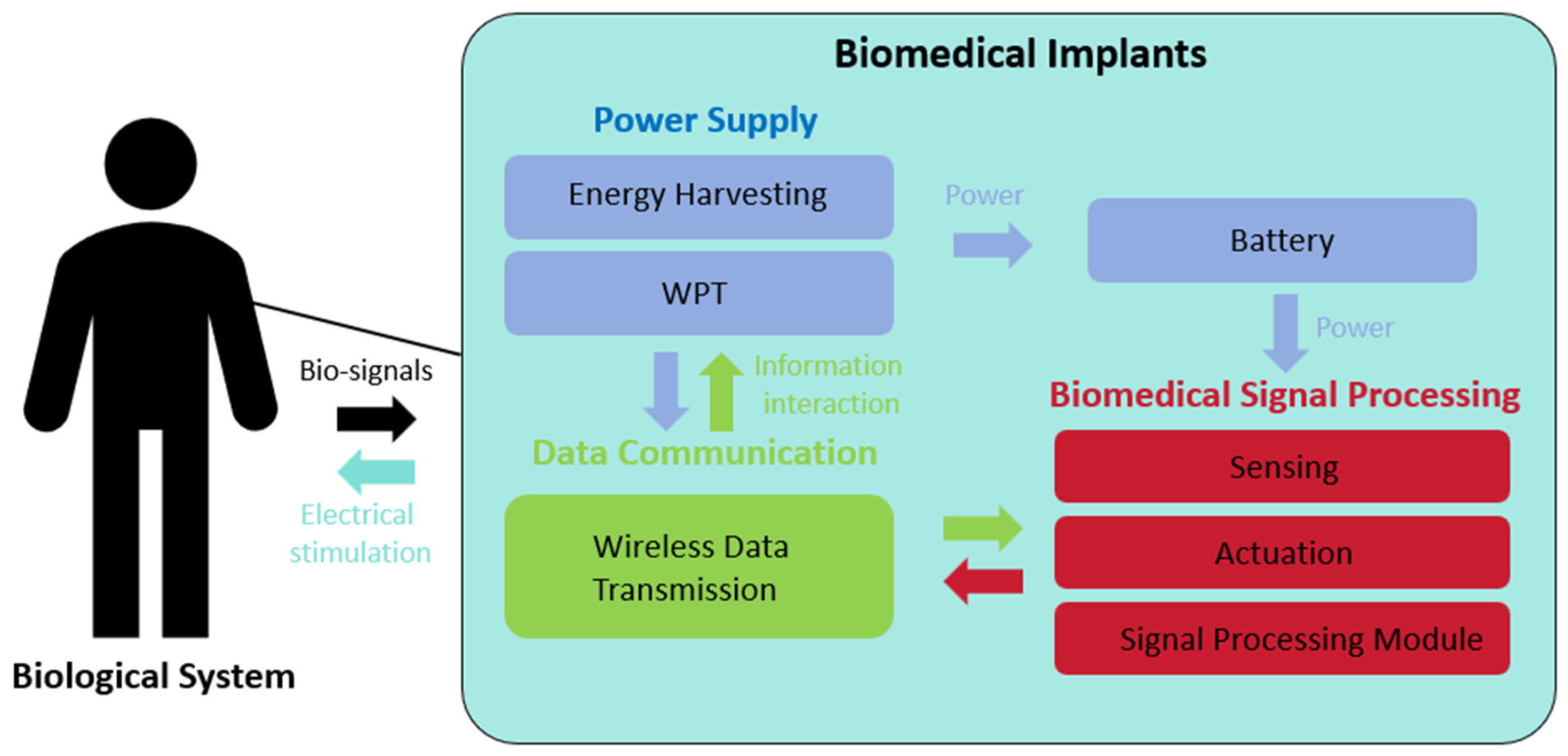
In the 1950s, the invention of the transistor paved the way for the proposal of implantable medical devices to aid patients. Since then, various systems such as cochlear implants, retinal prostheses, and neural prostheses have been widely developed. As depicted in Figure 1, these biomedical devices typically share similar internal functional modules. They comprise four primary functional modules: power supply, battery, data communication unit, and biomedical signal processing module. Although the power consumption of bio-implants is relatively low—where a mW-scale power output is usually sufficient to sustain normal operation—an onboard battery remains indispensable to fulfill the continuous power demands [9]. The volume of the battery is typically much larger than that of the internal circuitry, which explains why the overall size of implantable devices has not seen a significant reduction over the past few decades. To reduce battery size and facilitate energy supply, Wireless Power Transfer and Energy Harvesting have emerged as the primary power supply strategies for bio-implantable medical devices. Since WPT can deliver a much more stable power output than EH, it serves as the primary powering technique in most devices [10].
WPT systems can be broadly classified into near-field and far-field modalities, each demonstrating distinct application potentials for powering biomedical implants [11]. Near-field wireless power transfer, which relies on non-radiative electromagnetic fields for energy transmission, has emerged as the mainstream powering solution for bio-implants.
Near-field WPT is mainly divided into inductive and magnetic resonant coupling. Inductive coupling can achieve high efficiency under tight coupling but is highly sensitive to coil misalignment, making it more suitable for short-range powering of superficial implants [12,13,14]. In contrast, magnetic resonant coupling employs high-Q LC compensation networks to maintain efficient power transfer under weak coupling and spatial displacement. This characteristic is particularly valuable for implantable devices, where patient movement may cause lateral or angular coil misalignment. The operating frequency must balance receiver miniaturization and biosafety. Higher ISM frequencies, such as 6.78 MHz, reduce the required inductance and capacitance, enabling smaller receiving coils and more compact packaging. However, increased tissue absorption and thermal dissipation may raise SAR concerns. Therefore, careful resonant tuning and impedance matching are required to achieve stable and efficient power delivery within thermal and safety limits [15,16]. To meet the miniaturization requirements of implantable medical devices while complying with SAR and thermal safety constraints, future WPT systems will require increasingly compact coils and higher-efficiency rectifiers. The following sections provide a detailed analysis of the relevant design considerations.
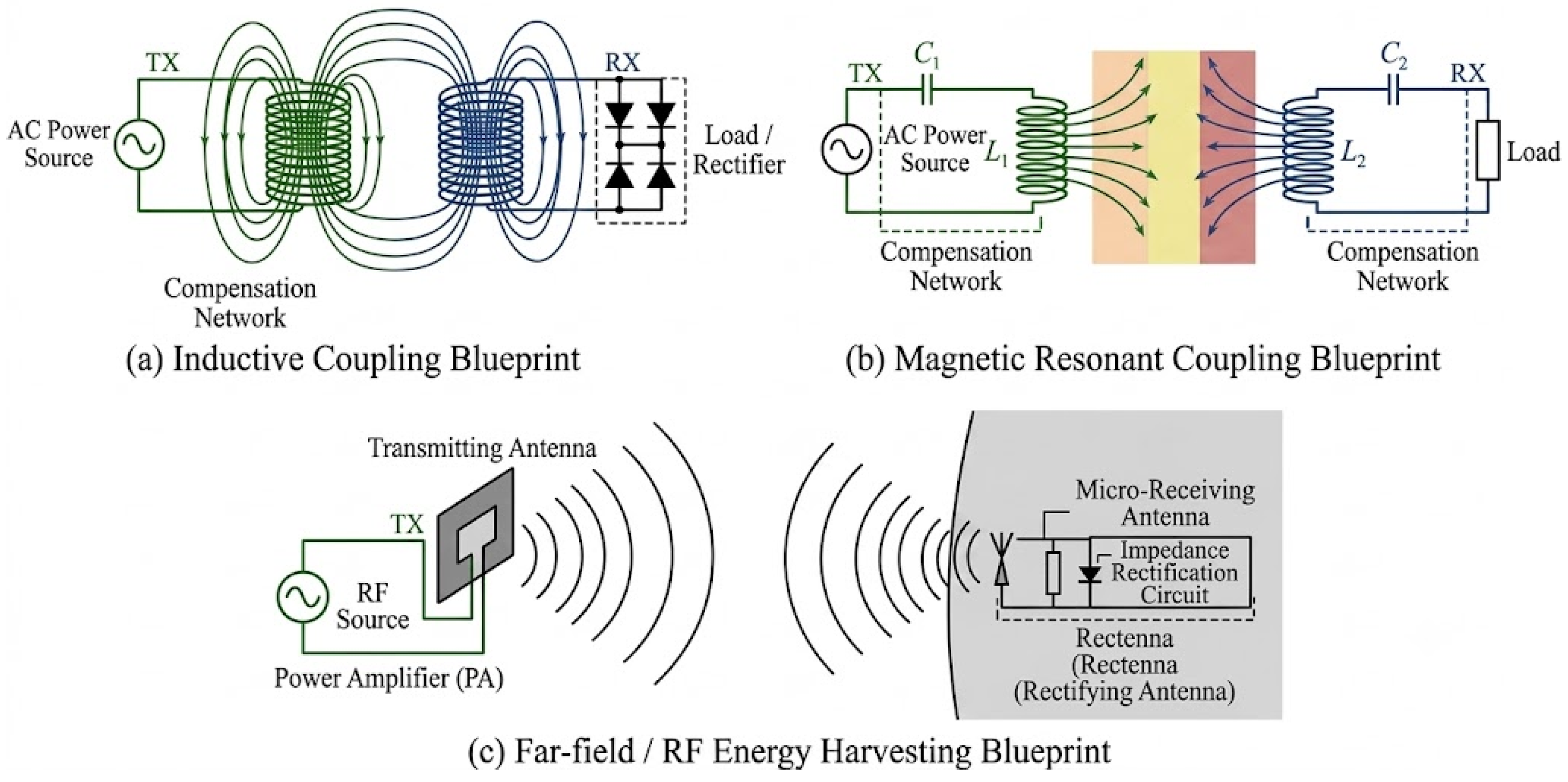
Conversely, far-field techniques utilize microwave or radio frequency (RF) waves to achieve long-distance energy transmission. This approach is capable of powering im-plants situated deeper within the body without necessitating precise alignment between the transmitter (TX) and receiver (RX). However, the widespread adoption of far-field WPT in bio-implants remains constrained by significant ongoing challenges, including severe tissue absorption, strict power density limitations, and safety concerns. Figure 2 illustrates the schematic diagrams of these three architectures [17,18,19].
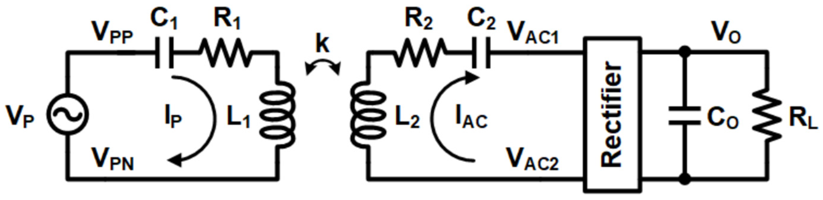
As the most prevalent powering mechanism for biomedical implants, magnetic resonant WPT systems have garnered substantial attention in recent years, with extensive research dedicated to enhancing transmission efficiency and expanding system functionality [20]. As shown in Figure 3, a typical resonant WPT architecture generally comprises a TX unit, an LC resonant link, an AC-DC converter, and a voltage regulation module. Furthermore, in state-of-the-art circuit designs, the biosensing signals acquired by the implantable devices can be transmitted back to external equipment via the receiving RX coil through backward data telemetry. Specifically, the TX front-end primarily consists of a power amplifier (PA) and a primary LC compensation network. Driven by an external power supply, the PA inverts the DC voltage into an AC voltage operating exactly at the target resonant frequency to excite the resonance. Upon capturing the transferred energy, the RX coil induces an AC voltage or current. The cascaded AC-DC converter then rectifies this AC energy into a stable DC voltage to supply the internal circuitry, thereby successfully accomplishing the power delivery from the ex vivo environment to the in vivo implant.
In light of the aforementioned analysis, this review focuses specifically on resonant WPT systems for bio-implantable devices, providing an in-depth analysis of state-of-the-art system architectures within this domain. The remainder of this paper is organized as follows. Section 2 introduces the commonly employed resonant topologies within resonant WPT systems. Section 3 analyses the challenges and evolutionary trends of WPT systems for bio-implants. Section 4 reviews recent advancements of integrated WPT systems applied to biomedical implants, with a particular emphasis on delay compensation techniques for active diodes and the technological evolution of regulating rectifiers. Finally, Section 5 concludes the paper.

2. Compensation Techniques for Magnetic Resonant WPT Systems

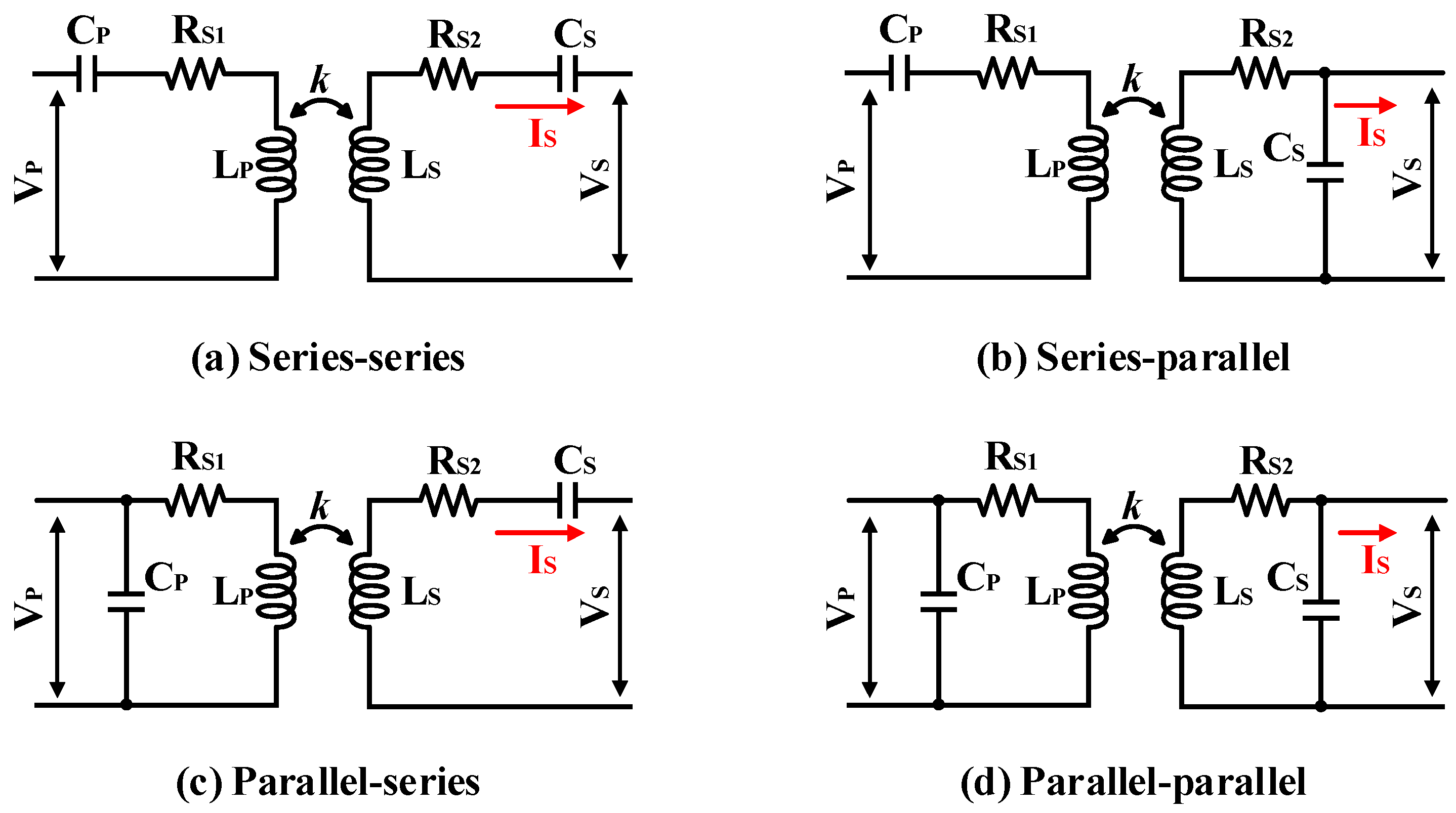
In resonant WPT systems, based on the connection configurations of the compensation capacitors at the transmitting and receiving sides, the system can be classified into four fundamental topologies: series-series (SS), series-parallel (SP), parallel-series (PS), and parallel-parallel (PP), as shown in Figure 4.
These four architectures exhibit distinctly different physical characteristics in terms of impedance matching, output profiles, and sensitivity to environmental variations. A distinguishing feature of the SS topology is that its primary and secondary resonant frequencies are entirely independent of variations in load impedance and the coupling coefficient. Under ideal resonance, it provides a constant-current output characteristic and effectively filters out high-order harmonics, making it the most stable and widely adopted structure to date [21,22]. The SP topology employs parallel compensation at the receiving end. Its secondary resonant tank possesses an inherent voltage amplification capability and exhibits a constant-voltage output characteristic, making it highly suitable for powering rectifier loads that require a stable high voltage for startup. However, the design of its resonant frequency is highly dependent on the coupling coefficient, rendering the system relatively sensitive to spatial misalignments [23,24,25,26]. In contrast, because the PS and PP topologies utilize parallel compensation at the transmitting end, they often require an exceptionally large input current to maintain the voltage across the magnetizing inductance [27]. Consequently, additional series inductors are typically required to form higher-order networks to suppress inrush currents from the power supply [28,29]. Because these two parallel-transmitter architectures impose extreme current stress on the inverter and are prone to severe overvoltage conditions during light-load or no-load operations, they are exceedingly rare in microsystem applications that demand low power consumption and high safety [30]. Instead, they are predominantly found in specific high-power industrial energy transfer scenarios. Table 1. shows the comparison of these topologies.
In implantable medical devices, both SS and SP resonant compensation networks are used for wireless power transfer, but they are usually selected for different power levels and load conditions [31]. In an SS topology, both the transmitter and receiver coils are compensated by series capacitors. The secondary side behaves more like a current-source interface, which is suitable for relatively low equivalent load resistance and high charging current. Therefore, SS compensation is more attractive in medium- to high-power implantable systems, such as implantable pumps, left ventricular assist devices, high-power stimulators, or rechargeable implants requiring fast battery charging. Its advantage is strong power-delivery capability and relatively simple current transfer behavior under heavy-load conditions. However, for small implants, SS compensation may suffer from insufficient voltage build-up at the rectifier input when the coupling is weak or the receiver coil is very small.
In contrast, the SP topology uses series compensation on the primary side and parallel resonance on the secondary side. The secondary parallel tank behaves more like a voltage-source interface, which is more suitable for low-power and medium-power biomedical implants with relatively high equivalent load resistance. Examples include neural recording systems, brain–computer interface implants, cochlear implants, retinal prostheses, and low-power sensor nodes. These systems usually require tens of milliwatts to several hundred milliwatts, and the key design target is to generate enough AC voltage at the receiver for efficient rectification and regulation rather than to deliver a large current directly. SP compensation is therefore commonly preferred in loosely coupled, miniaturized implantable systems. It also matches well with active rectifiers and post-regulation or battery-management circuits. In summary, SP compensation is generally more common in low- to medium-power implantable medical devices, while SS compensation becomes more suitable when the implant requires higher power, larger charging current, or lower load impedance.
Coil misalignment caused by body motion or implant displacement is a major prac-tical challenge in biomedical resonant WPT systems. Lateral, angular, and axial misa-lignments alter the mutual inductance and reflected impedance of the inductive link, leading to resonant detuning, reduced received voltage and power, and degraded transfer efficiency [32]. In addition, coil deformation caused by body motion can vary the coil in-ductance and further shift the resonant frequency [33]. At the link level, misalignment tol-erance can be improved through misalignment-resilient coil geometries and multi-coil or relay-resonator structures, impedance matching and automatic resonance tuning, and closed-loop TX–RX power control [34,35,36,37]. Misalignment tolerance can also be improved us-ing overlapping transmitter-coil arrays. For example, a star-shaped array generates mag-netic-field components in different directions, allowing the receiver to continue receiving power under large angular misalignment and rotation [38]. Nevertheless, these methods involve tradeoffs among coverage range, implementation complexity, power consumption, and safety. The resulting variations in receiver input amplitude and phase also affect the operation of the rectifier and voltage-regulation circuits, as discussed in the following section.
Biological tissue also affects implantable WPT performance. Although tissue is ap-proximately nonmagnetic and coil geometry and alignment mainly determine the mutual inductance, tissue thickness and electrical properties still influence the resonant link. The frequency-dependent conductivity and permittivity of skin, fat, muscle, and bone intro-duce loss and parasitic loading, which can change the coil impedance, reduce the loaded quality factor, and detune the resonant link. As a result, the received voltage, available power, and transfer efficiency may decrease even when the coils are well aligned [39]. In addition, different implantation sites and tissue changes, such as scar formation, can fur-ther shift the resonant condition, making fixed compensation less reliable [40]. These effects can be evaluated using electromagnetic simulations with multilayer or anatomically real-istic tissue models, from which the coil impedance, quality factor, coupling coefficient, and link efficiency can be extracted. The simulation results should be further validated by measuring the link response in tissue-equivalent phantoms or ex vivo tissue. Therefore, tissue properties should be included in the link design, while adaptive tuning, impedance matching, and TX–RX power control can improve robustness under tissue- and cou-pling-dependent variations.
In addition, data-driven methods are emerging as useful tools for handling the mul-tidimensional tradeoffs in implantable WPT design. Recently, an ANN model trained us-ing finite-element data was employed to optimize high-frequency inductive links for effi-ciency and size under SAR constraints [41].

3. Challenges and Evolutionary Trends of WPT for Bio-Implants

3.1. Thermal Safety and SAR Constraints

Thermal safety and specific absorption rate (SAR) constraints are critical considerations in implantable WPT systems. According to the ICNIRP 2020 Guidelines for radiofrequency electromagnetic-field exposure, the localized SAR for the general public should not exceed 2 W/kg in the head and torso or 4 W/kg in the limbs, averaged over a cubic 10-g tissue mass and a 6-min exposure interval [42]. In addition, ISO 14708-1:2014, which specifies general safety requirements for active implantable medical devices, adopts a maximum temperature-rise criterion of 2 °C above the normal surrounding body temperature for the external surface of an implanted device [43]. Although increasing the operating frequency facilitates receiver-coil miniaturization, it may increase electromagnetic absorption in biological tissue and reduce the safely deliverable power [13,44]. The resulting temperature rise originates from both electromagnetic energy absorbed by tissue and power losses in the implanted coil, rectifier, regulator, and other circuit components [45]. Therefore, maximizing power-transfer efficiency alone does not necessarily maximize the power that can be safely delivered; instead, the maximum deliverable power under SAR and temperature-rise constraints should be considered during the joint optimization of the operating frequency, coil geometry, compensation topology, and load conditions [46]. Moreover, nonuniform magnetic fields and coupling variations may create localized hot spots or excessive received power. Field-homogenizing coil structures, resonance detuning, and closed-loop transmitter power control can alleviate these risks [47]. Consequently, implantable WPT systems should be evaluated through combined electromagnetic, circuit, and thermal analyses under realistic implant depths, misalignment conditions, coupling variations, and load conditions.
Long-term in vivo operation introduces additional reliability challenges beyond the initial SAR and temperature requirements. Package aging, moisture ingress, material corrosion, repeated body motion, and tissue changes around the implant may alter the coil impedance, coupling condition, and heat dissipation, leading to resonance drift, reduced transfer efficiency, output instability, or increased local temperature. Therefore, implantable WPT systems require biocompatible moisture-resistant encapsulation, mechanically robust coils and interconnects, adaptive tuning and power control, and voltage and temperature protection. Long-term stability should also be evaluated through accelerated aging, saline-soak, thermal-cycling, mechanical-fatigue, and continuous power-transfer tests.
At the IC level, the active rectifier should be designed to minimize both implant self-heating and the transmitter power required to support the target load. Although rectifier losses do not directly contribute to tissue SAR, conduction loss, body-diode conduction, reverse current, switching loss, and control-circuit overhead are dissipated locally within the implant, thereby increasing the temperature of the chip and surrounding tissue. Meanwhile, a low rectifier efficiency requires a higher transmitted power, which indirectly increases electromagnetic exposure and SAR. Therefore, adaptive on/off delay compensation, low-quiescent-power comparators and controllers, and high-efficiency regulation over wide input-power and load ranges are essential, particularly at high operating frequencies.

3.2. Evolutionary Trends of WPT for Bio-Implants

Implantable medical devices are increasingly being developed toward miniaturization to reduce surgical complexity, tissue damage, and patient discomfort. In a typical wirelessly powered implantable system, the RX coil, power-management circuitry, and battery are among the major contributors to the overall device volume. Continuous or periodic wireless power delivery provides a potential approach to reducing or even eliminating the dependence on bulky batteries. Meanwhile, advances in integrated-circuit technologies allow rectifiers, voltage regulators, and control circuits to be implemented at the chip level, thereby substantially reducing the volume occupied by the power-conversion circuitry. Consequently, the RX coil remains one of the principal constraints on further system miniaturization.
Increasing the operating frequency has therefore been widely considered an effective approach to reducing the required RX-coil inductance. For the RX side of the SP resonant topology commonly employed in implantable wireless power transfer systems, the resonant frequency ω can be expressed as
ω = 1 L R X C R X  
where LRX and CRX denote the resonant inductance and resonant capacitance at the RX side, respectively, and ω represents the resonant angular frequency.
According to (1), increasing the resonant frequency can substantially reduce the required inductance and physical dimensions of the RX coil. Consequently, recent studies on WPT systems for implantable medical devices have progressively increased the operating frequency from 6.78 MHz to 13.56 MHz and even 40.68 MHz. However, this trend also introduces several additional challenges, including increased switching losses and reduced rectification efficiency at high frequencies, potential thermal-safety risks caused by high-frequency reverse current, and more stringent SAR constraints.
In addition, recent studies have addressed detuning caused by coil variations and fluctuations in coupling. In [33], a phase-shift-detection-based resonant-frequency compensation method was proposed, in which the duty cycle of a switched TX-side resonant capacitor is controlled to retune the resonant point and improve efficiency under detuned conditions; In [37], a hybrid voltage-/current-mode receiver structure was proposed to achieve output-voltage recovery under weak-coupling conditions through multi-cycle resonant energy accumulation and current-mode power delivery.
Looking ahead, emerging technologies are expected to further improve the adaptability and miniaturization of implantable WPT systems. Artificial-intelligence-assisted power optimization may enable real-time prediction of coupling variations, load demands, and detuning conditions, allowing the operating frequency, transmitted power, and rectifier control parameters to be adjusted adaptively. Meanwhile, flexible electronics and stretchable implants can improve mechanical conformity with biological tissues, although deformation-induced variations in coil characteristics must be carefully addressed. Energy-aware power-management strategies can further coordinate rectification, voltage regulation, energy storage, and load scheduling according to the available received power, thereby enhancing system efficiency, reliability, and operational lifetime under dynamically varying in-vivo conditions.
Accordingly, chip-level control and optimization of rectifiers have become important research topics in recent years. The remainder of this section reviews representative delay-compensation rectifiers for high-frequency resonant operation, as well as advanced regulating-rectifier IC architectures.

4. Technological Evolution of Integrated Rectifiers for Bio-Implants

4.1. Conventional AC-DC Converters

As previously discussed, the energy at the transmitting (TX) side is converted into alternating current (AC) power via the resonant circuit. For biomedical implants, the allowable wireless power transfer level is substantially lower than that of conventional smart electronic devices. Furthermore, this available power undergoes severe attenuation as it propagates through the tissue layers. Consequently, to ensure that the medical device harvests sufficient power while rigorously minimizing in vivo heat dissipation, an exceptionally high-efficiency AC-DC converter is imperative to execute the AC-to-DC energy conversion [10].
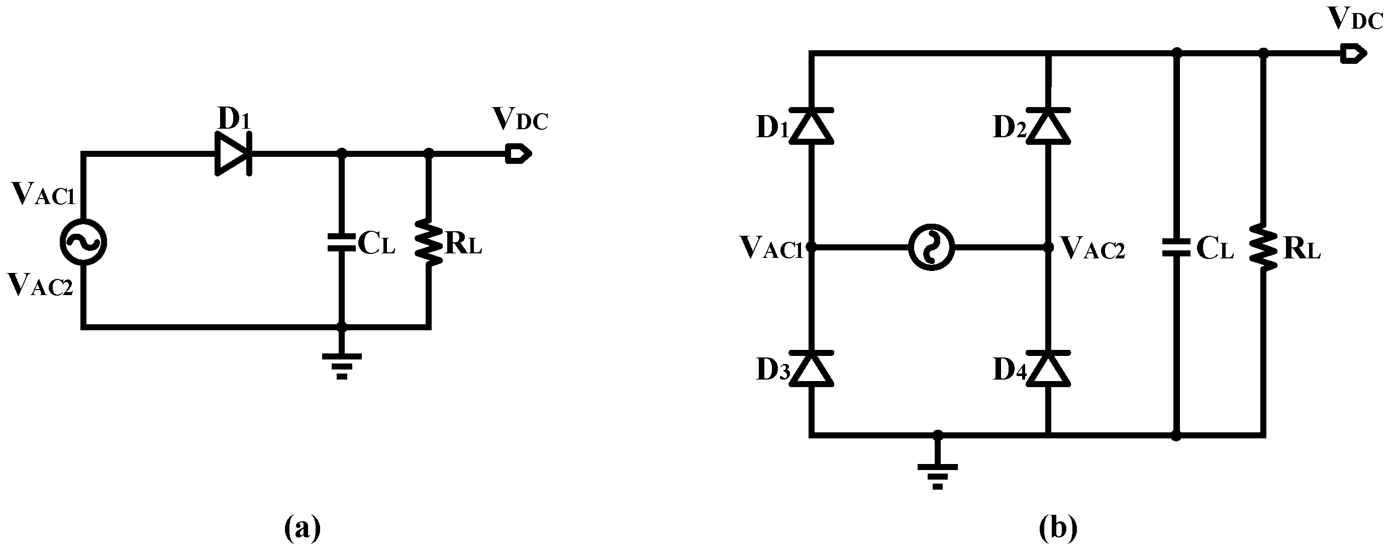
A rectifier is a prevalent converter utilized for AC-DC conversion, typically composed of diodes. In integrated circuit design, passive diodes can be implemented using PN junctions or diode-connected MOSFETs. Figure 5 illustrates two common rectifiers.
Figure 5a shows a half-bridge rectifier. When the AC voltage source outputs an alternating voltage, node VAC1 outputs a high voltage when VAC1 − VAC2 > 0 V, due to the unidirectional conductivity of the diode. When VAC1 − VDC > VTH, diode D1 becomes forward-biased and turns on, allowing current to flow through the diode into the load. Under other conditions where VAC1 − VDC < VTH, diode D1 is reverse-biased. The loop between the voltage source and the load is disconnected, preventing energy from being delivered to the load. For the SP resonant circuit, the receiving (RX) end behaves as a voltage source; therefore, current is output only during the positive half-cycle. However, the SS resonant circuit behaves as a current source at the RX end. Although it can normally output current during the positive half-cycle, the reverse current during the negative half-cycle causes a drastic voltage drop at VAC2, which can easily cause the diode to exceed its voltage rating. Consequently, this type of rectifier is not suitable for the SS resonant topology.
As for the full-bridge rectifier shown in Figure 5b, D1 and D4 conduct to form a current loop during the positive half-cycle when VAC1 − VAC2 > VDC + 2VTH. Conversely, D2 and D3 conduct during the negative half-cycle when VAC2 − VAC1 > VDC + 2VTH. In this way, current output is achieved during both half-cycles of the AC source. Furthermore, because the current source has a corresponding current path in every phase, overvoltage issues are averted. Therefore, this full-bridge rectifier is applicable to both SS and SP topologies.
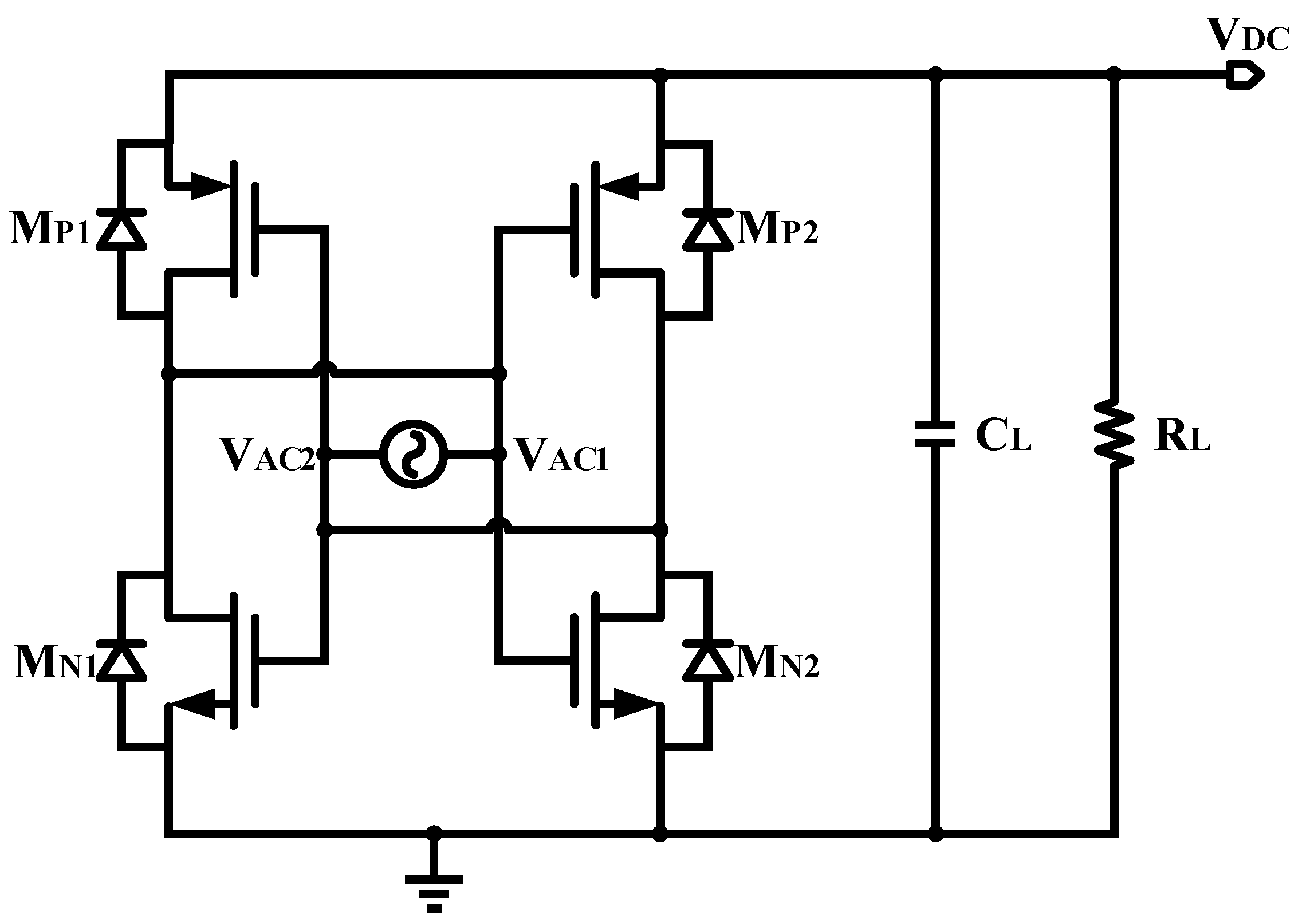
Figure 6 illustrates the cross-coupled rectifier. Unlike conventional diode-based rectifiers, this architecture utilizes VAC1 and VAC2 to drive the MOSFETs, thereby achieving a low on-resistance and strictly limiting the forward voltage drop [48]. At low input voltages, both the reverse current and short-circuit current of the rectifier are significantly suppressed. However, this is accompanied by an increase in on-resistance, making the topology highly suitable for ultra-low-power applications. Nevertheless, if the instantaneous input voltage is excessively high during state transitions, the PMOS and NMOS transistors may turn on simultaneously, leading to substantial leakage current and energy dissipation.
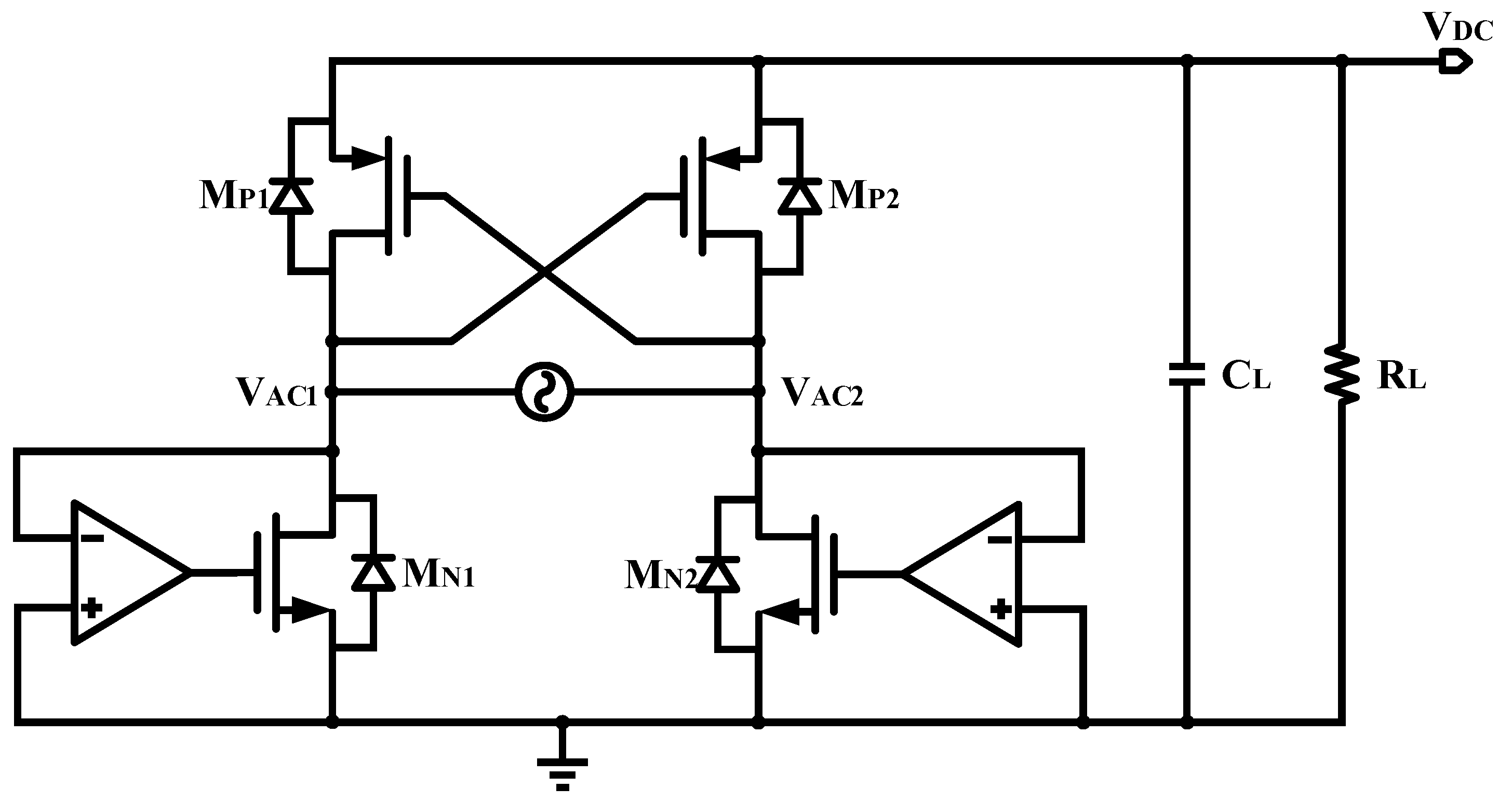
The active full-wave rectifier illustrated in Figure 7 is a widely adopted architecture in modern biomedical implants. By replacing two conventional diodes in a standard full-bridge rectifier with active diodes, while configuring the remaining two MOSFETs in a cross-coupled pair, this topology successfully combines the advantages of both diode-based and cross-coupled rectifiers [49]. Consequently, it not only minimizes the forward voltage drop but also eliminates the shoot-through issues under high input voltages. Its operational principle is described as follows. For the series-parallel (SP) configuration, the AC input VAC acts as a voltage source. When VAC2 − VAC1 > VTH,P, MP2 turns on, clamping VAC2 to VDC. Subsequently, as VAC1 drops below the ground potential, the comparator CMP2 outputs a high level to turn on MN2, enabling the input current IAC to charge VDC through the conduction path formed by MP2 and MN2. When VAC1 rises back above the ground level, CMP2 deactivates MN2, thereby terminating the power delivery phase. During the subsequent half-cycle, the rectifier symmetrically controls MP1 and MN1 to complete the corresponding rectification phase, achieving full-wave operation.
For the series-series (SS) topology, the input behaves as a current source IAC. When the current flows from VAC2 to VAC1, VAC2 drops below ground while VAC1 rises. This triggers the conduction of CMP1 and MP1 while MP2 turns off, allowing IAC to charge VDC via MP1 and MN1; the opposite half-cycle operates analogously. Distinct from the SP topology, the current-source characteristic of the SS configuration drives rapid voltage transitions on VAC1 and VAC2, which typically extends the charging phase across the entire half-cycle. Although the integration of active diodes effectively reduces the forward voltage drop while mitigating shoot-through and reverse-current issues under high input voltages, it inevitably requires active comparators. This introduces additional silicon area and power consumption overhead. Furthermore, since these comparators are powered directly by the rectified output voltage VDC, the startup mechanism of the circuit warrants careful consideration.

4.2. Delay Compensation Techniques

4.2.1. State-of-the-Art Delay Compensation Architectures

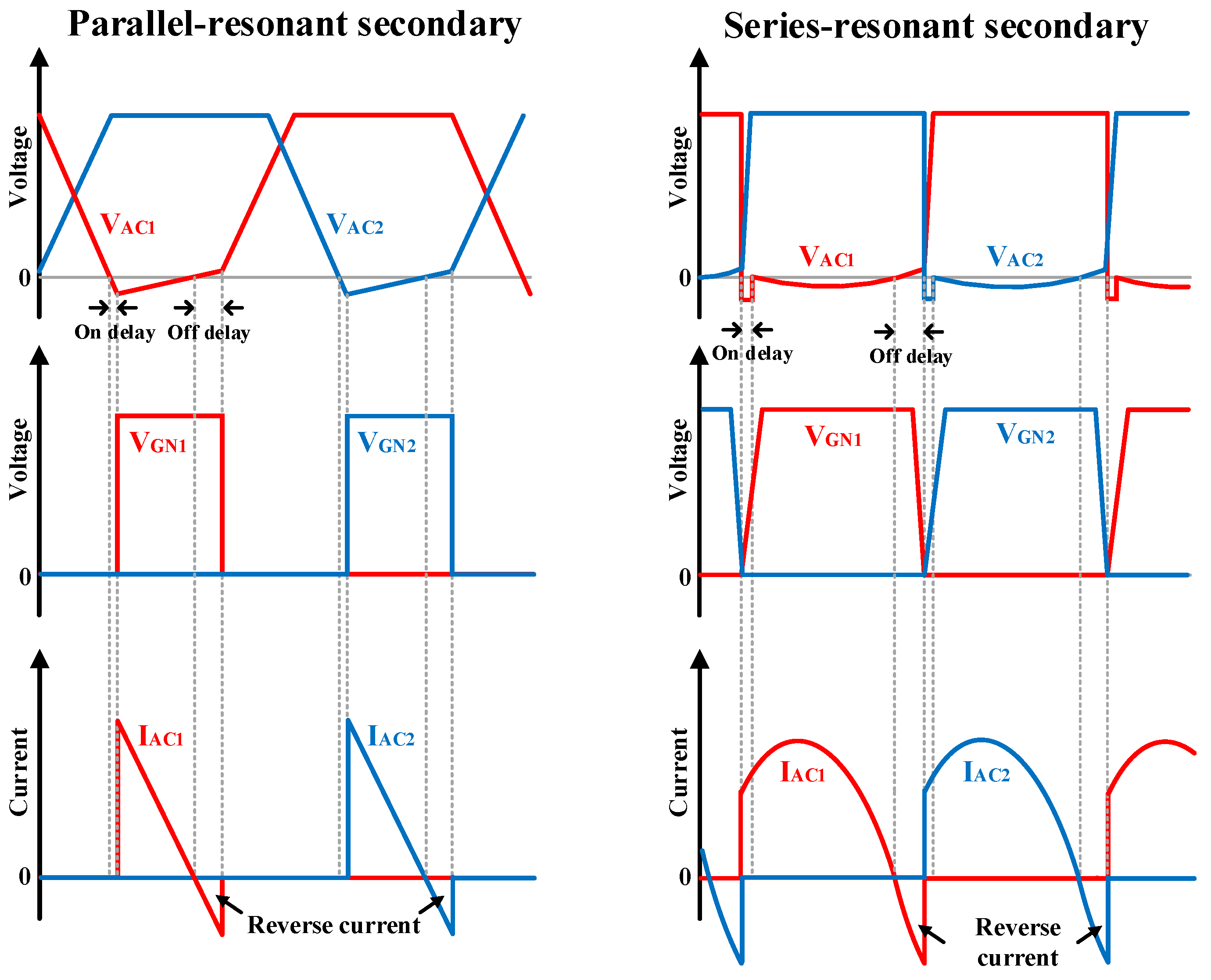
As discussed above, the comparator delay in an active rectifier affects the rectifier’s efficiency to varying degrees. In an SS-type resonant circuit, a turn-on delay causes the body diodes of MN1 and MN2 to conduct, while a turn-off delay leads to reverse current. For an SP-type resonant circuit, a turn-on delay shortens the switch conduction time and increases the peak current, and a turn-off delay similarly introduces reverse current. Figure 8 illustrates the corresponding rectifier voltage and current waveforms for the two compensation topologies.
In SP topology resonant circuits, both turn-on and turn-off delays degrade the active rectifier’s power conversion efficiency (PCE) and voltage conversion ratio (VCR), with turn-off delays exhibiting a more pronounced impact under light-load conditions. In SS-topology resonant circuits, however, the rectifier’s PCE experiences only a marginal decline, presenting a stark contrast to the SP topology [50,51,52,53,54,55,56]. This disparity arises because, in SP circuits, turn-off delays prolong the conduction time of the power transistors, inducing additional conduction losses. Furthermore, at high operating frequencies, comparator and gate-driver delays occupy a larger portion of the switching period. In particular, the turn-off delay duration may become comparable to the forward current conduction time increasing body-diode conduction and reverse-current loss. These additional conduction losses can severely degrade the PCE, making delay compensation essential for maintaining high active-rectifier efficiency.
Conversely, in SS circuits, turn-off delays merely alter the current path without exacerbating transistor conduction losses, thereby limiting the efficiency drop. Nevertheless, the resultant reverse current diminishes the total current delivered to the load in the series-resonant circuit, compelling an increase in the energy output from the transmitter.
Since comparator offset and propagation delay vary with process, supply voltage, and temperature, a fixed compensation value may become insufficient or excessive, thereby increasing body-diode conduction and reverse-current loss. The adaptive delay-compensation techniques reviewed above track the optimum turn-on and turn-off instants and therefore improve the VCR and PCE across PVT variations.
Based on the above analysis, the switching delay significantly impacts the energy conversion efficiency of the parallel resonant secondary side. Therefore, precise delay compensation is essential for the comparators in active diodes. Traditional compensation methods typically introduce a constant offset, utilizing unbalanced currents or asymmetric input transistors to achieve delay compensation. For instance, in [50], a bias voltage is applied to the comparator exclusively during the turn-off phase of the transistor and is removed during the turn-on phase. Although several similar schemes have been proposed in [49,51,52,53,54] to mitigate switching delay, their delay characteristics fluctuate under PVT variations, making precise compensation unachievable.
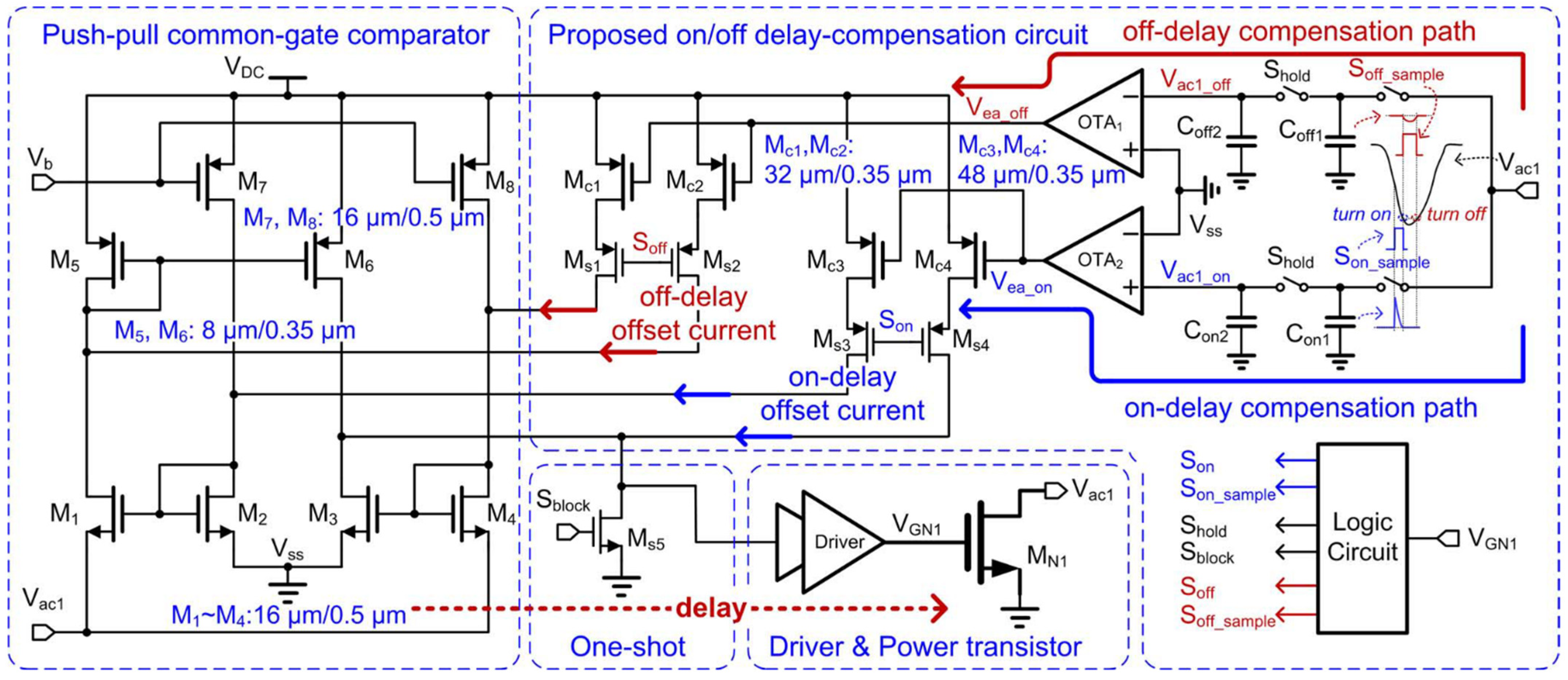
To address this, an adaptive switching delay compensation rectifier was proposed in [57], which dynamically adjusts the compensation current in real time based on the switching states to achieve accurate delay compensation. The architecture of this compensation scheme is illustrated in Figure 9. By sampling the VAC voltage at the switching instants, it compensates for the turn-on and turn-off delays respectively based on the sampled voltage. Since this method adjusts dynamically according to the real-time switching states, it maintains switching accuracy across PVT variations. Consequently, this approach can significantly improve the power conversion efficiency of the parallel resonant secondary. As an early approach, this delay compensation method effectively compensates for comparator offset and delay, thereby improving the VAR and PCE of the rectifier. A similar delay compensation method is also adopted in [58] to improve the rectifier’s performance.
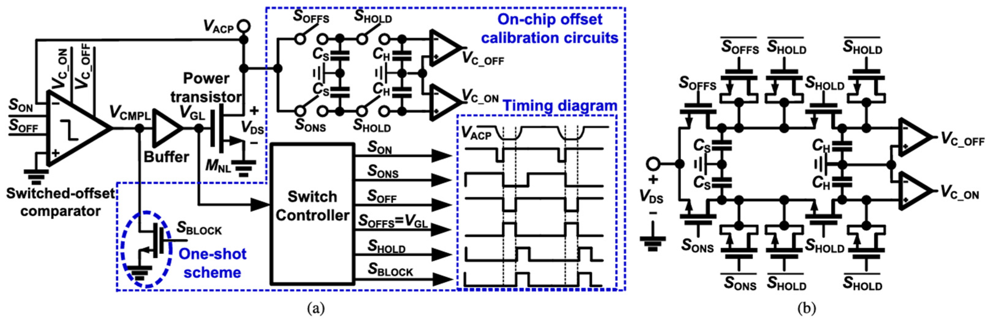
Noh et al. proposed a voltage-mode switched-offset comparator for a 13.56 MHz CMOS active rectifier [59]. As shown in Figure 10, this method still belongs to the category of switched-offset delay compensation. Its basic principle is to intentionally introduce turn-on and turn-off offset voltages, so that the comparator switches before the input voltage reaches the ideal transition point, thereby compensating for the propagation delays of the comparator and the subsequent buffer. Unlike the conventional current-mode switched-offset comparator, this structure does not generate the input-referred offset by injecting additional ION and IOFF. Instead, it directly injects adjustable VON and VOFF inside the comparator. Specifically, VON is used to trigger the turn-on of the power NMOS transistor in advance, thereby extending the effective conduction time, whereas VOFF is used to advance the turn-off transition and reduce reverse current.
In contrast, the voltage-mode approach reuses the original bias current of the comparator to generate continuously adjustable offset voltages. As a result, it can reduce comparator power while maintaining the delay-compensation function. Since the power loss of the comparator and calibration circuits accounts for a larger proportion of the total loss under light-load conditions, this method is particularly effective in improving light-load efficiency.
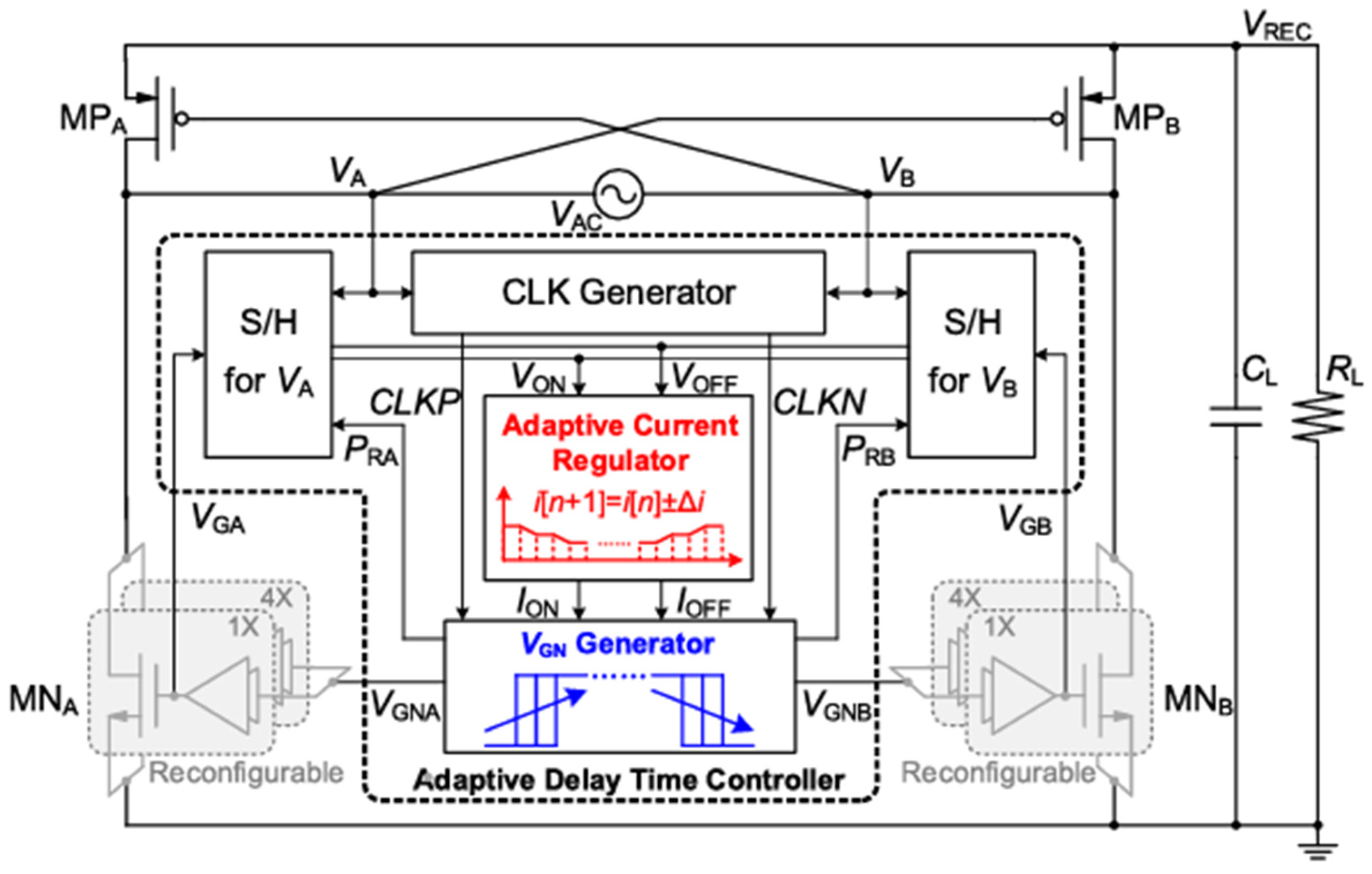
Based on the reduction of power consumption in switched-offset comparators, subsequent studies further attempted to reduce or even eliminate the power overhead introduced by high-speed continuous-time comparators from the perspective of control methodology. Xue et al. proposed an active rectifier architecture based on adaptive delay-time control [60], as shown in Figure 11. Unlike conventional comparator-based approaches that directly detect the zero-crossing point to determine the turn-on and turn-off instants of the power switches, this method no longer relies on high-speed comparators for real-time switching decisions. Instead, current-controlled delay lines are used to generate the optimal switching instants of the power NMOS transistors. The basic idea is to convert the turn-on and turn-off instants into adjustable delay quantities and to regulate these delays cycle by cycle through a tracking algorithm similar to successive approximation, so that the sampled turn-on and turn-off errors gradually converge within an acceptable range.
Through this step-by-step approximation process, the actual turn-on and turn-off instants of the power transistor eventually approach the zero-voltage switching point, thereby extending the effective conduction time and suppressing reverse current. The key feature of this scheme is that delay compensation is shifted from comparator threshold adjustment to time-domain delay adjustment, which avoids the static power consumption associated with high-speed comparators and large offset-injection currents. In addition, since only one gate-drive signal is generated in each cycle, the multiple-pulsing problem can also be alleviated.
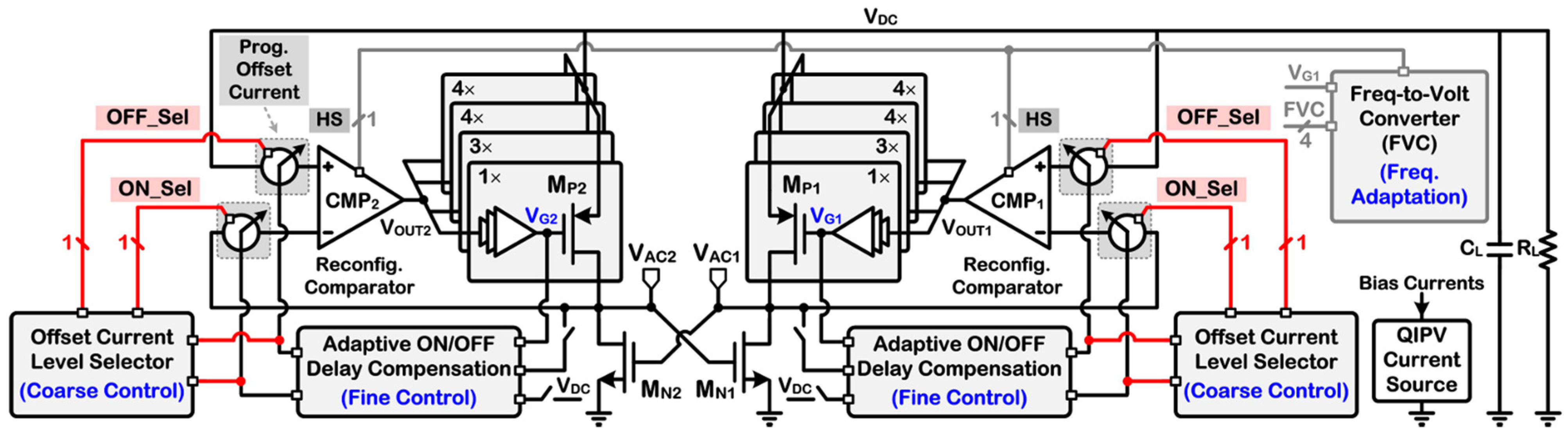
In applications with variable operating frequencies, more flexible delay-compensation schemes are required to maintain high rectifier efficiency. To accommodate rectifier operation under varying input-frequency conditions, Erfani et al. proposed a frequency-aware active rectifier with dual-loop adaptive delay compensation for capacitive wireless power transfer, as shown in Figure 12 [61]. The proposed rectifier combines switched-offset-current-based delay compensation with a dual-loop control architecture, in which a fine-control loop provides high-resolution on/off delay calibration, while a coarse-control loop extends the available compensation range by reconfiguring additional offset-current branches. Compared with conventional adaptive delay-compensation schemes with a fixed maximum offset current, this approach achieves both fine timing accuracy and a wider dynamic compensation range. Moreover, by introducing frequency-aware comparator reconfiguration through a frequency-to-voltage converter, the rectifier can adapt to input-frequency variations from 1 to 10 MHz, making it suitable for wide-frequency, wide-load-range, and high-power capacitive WPT applications.
As mentioned above, the current-injection approach can advance the comparator transition by introducing an artificial offset. However, at high operating frequencies, it requires a relatively large injection current and a short timing window, which leads to high power consumption. In contrast, the delay-line-based approach consumes less power and helps avoid the multiple-pulsing problem, but conventional delay-line structures are mainly used for turn-off delay compensation.
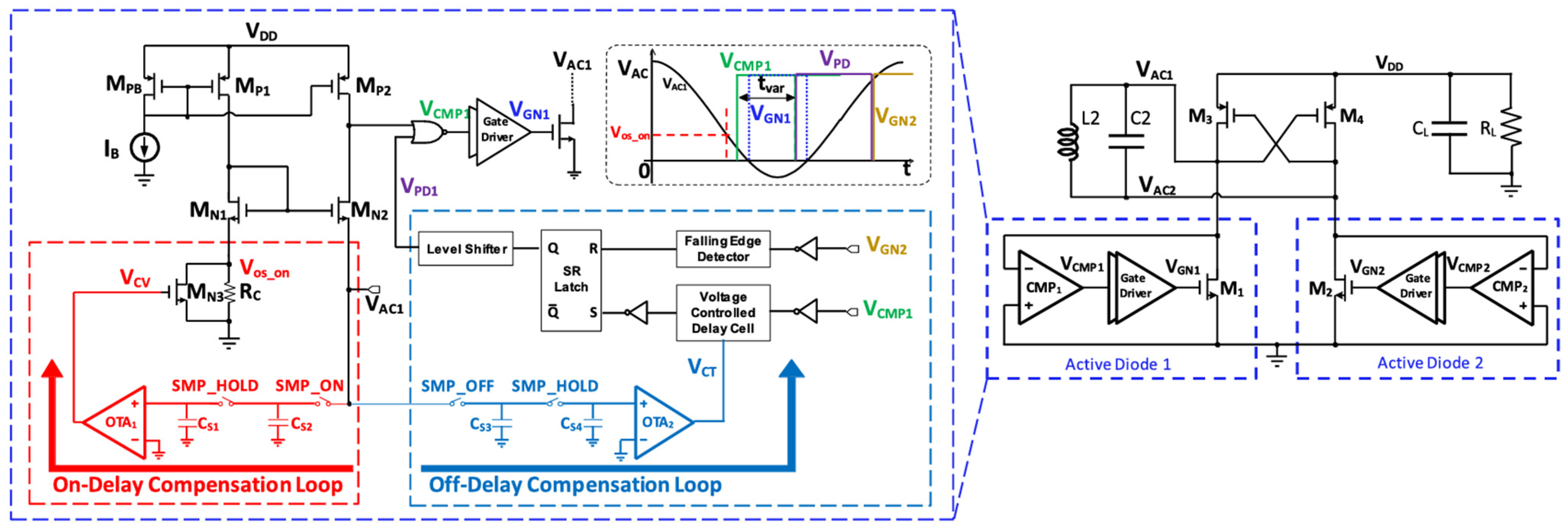
As the operating frequency further increases to 40.68 MHz, conventional current-injection-based switched-offset compensation faces more stringent power and timing constraints. Cheng et al. proposed a hybrid adaptive on/off delay-compensation scheme for high-frequency wirelessly powered implantable receivers, as shown in Figure 13. This scheme combines voltage-based turn-on compensation with delay-based turn-off compensation [62]. For turn-on compensation, an adjustable offset voltage is introduced at the comparator reference terminal, allowing the power NMOS transistor to turn on earlier, thereby reducing body-diode conduction and improving the VCR. For turn-off compensation, an adjustable delay is used to control the pull-down signal, so that the comparator output is reset at an appropriate instant. As a result, the power transistor can be turned off earlier, and the reverse current can be suppressed. Since this scheme does not require conventional current-injection offset, the comparator power consumption is reduced. Meanwhile, the delay-based turn-off control helps avoid multiple triggering.
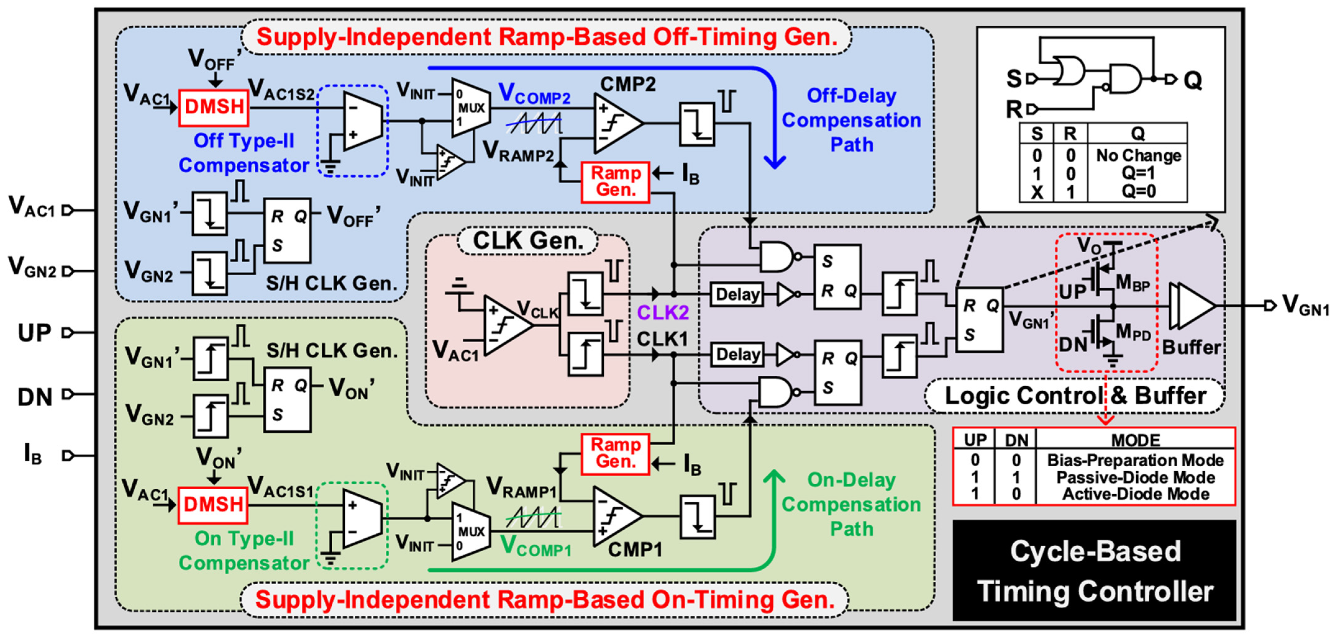
As shown in Figure 14, Luo et al. proposed a cycle-based on/off delay compensation method for 40.68-MHz active rectifiers used in high-current implantable systems [63]. Unlike conventional edge-triggered schemes, whose compensation range is limited by the short zero-crossing interval, this method generates a supply-independent voltage ramp over the entire input cycle and determines the turn-on and turn-off timing through ramp comparison and sample-and-hold circuits. Therefore, the available compensation window is extended to the full cycle, enabling a wider timing-adjustment range and more complete delay compensation at high frequency. With the aid of a delay-mimicking sample-and-hold circuit and a low-voltage-stress startup scheme, the rectifier improves both timing accuracy and device reliability, achieving high output power, high voltage conversion ratio, and high power conversion efficiency in compact-coil implantable WPT applications.

4.2.2. Comparison of Delay Compensation Techniques

The delay-compensation techniques summarized in Table 2 show a clear transition from comparator-offset correction to adaptive time-domain timing control, where the PCE and VCR are defined as follows:
P C E = P o u t P i n × 100 %
V C R = V o u t V o u t , i d e a l × 100 %
The impact of switching delay first depends on the compensation topology. In an SP-compensated receiver, the input behaves as a voltage source, and the available conduction interval becomes short at high frequencies or light loads. Turn-on delay reduces the charge-transfer interval, whereas turn-off delay produces additional conduction loss and reverse current, causing pronounced degradation in both PCE and VCR. In an SS-compensated receiver, the resonant current is mainly determined by the LC tank, and switching delay primarily changes the current path. Therefore, the PCE is generally less sensitive to delay, although reverse current still reduces the net power delivered to the load and increases the required TX power. Consequently, precise adaptive delay compensation is more critical for high-frequency SP receivers, while SS receivers may prioritize reliable current commutation and low control overhead.
Fixed-offset techniques in [49,50,51,52,53,54] provide simple implementations for systems with limited operating variations, but their compensation accuracy deteriorates under PVT changes. Adaptive current-mode schemes, such as [57,58], dynamically adjust the compensation current and improve timing robustness, although their sampling circuits, current-injection branches, and continuously biased comparators increase static power and chip area. Voltage-mode switched-offset compensation [59] reduces the required offset-current overhead, but still requires adjustable voltage generation and high-speed comparison. Its reported peak PCE of 86.1% is lower than the 91.4% achieved in [57], although this difference cannot be attributed solely to the compensation principle because their power levels and circuit implementations differ.
Time-domain control [60] generates the required switching instants using adjustable delay lines rather than comparator offsets. It reports a peak PCE of 94.1% and an area of only 0.117 mm2, demonstrating an attractive efficiency–area trade-off for compact 13.56-MHz implants. However, its compensation range is limited by the delay-line tuning range. The dual-loop architecture in [61] combines fine and coarse adjustment to support a wider frequency range of 1–10 MHz and an output power of 231.6 mW, but frequency detection, loop switching, and multiple control branches increase complexity and control consumption. It is therefore more suitable for wide-range systems than for fixed-frequency, ultra-low-power implants.
At 40.68 MHz, the shortened switching period makes conventional offset-current compensation increasingly inefficient. The hybrid scheme in [62] separately applies voltage-mode turn-on compensation and delay-mode turn-off compensation, reducing the required offset current, but its peak PCE and VCR are limited to 80.9% and 84.1%, respectively. In comparison, the cycle-based method in [63] extends the compensation window to the entire input cycle and achieves a VCR of 96.3% at an output power of 207 mW. This wider timing range is obtained at the cost of additional ramp-generation, sampling, and delay-mimicking circuits, while its peak PCE of 85.1% indicates that high-frequency switching and gate-driving losses remain significant.
Overall, fixed-offset methods provide low complexity, adaptive current- and voltage-mode schemes improve PVT robustness, time-domain control offers favorable efficiency and area at 13.56 MHz, dual-loop control supports wider operating ranges, and hybrid or cycle-based techniques are more suitable for 40.68-MHz operation. Therefore, the appropriate architecture should be selected according to the resonant topology, operating frequency, coupling variation, output-power range, allowable control overhead, and required compensation range, rather than according to peak PCE or VCR alone.

4.3. Regulating Rectifier Techniques

4.3.1. State-of-the-Art Regulating Rectifier Techniques

At the receiver side, a WPT system needs to tolerate output load transients. When the load changes, the output current varies rapidly, which causes disturbances in the output voltage. A conventional RX usually employs an LDO [64,65] or a DC–DC converter [66,67,68,69] after the rectifier to generate a regulated output voltage. However, such a two-stage topology degrades power conversion efficiency and increases chip area as well as system cost. To improve efficiency, voltage regulation can be integrated into the rectifier, leading to the concept of a single-stage regulating rectifier.
For a SS resonant compensation network, the series-resonant tank at the RX side can be regarded as a current-source-like input to the rectifier. Based on this characteristic, the rectifier can be reconfigured to provide different equivalent output-current levels. By controlling the duty ratio of different operating modes within one modulation period, the rectifier can regulate the output voltage while simultaneously performing AC–DC conversion. Compared with the conventional two-stage topology, the single-stage regulating rectifier reduces cascaded power loss and relaxes the requirement for off-chip passive components, making it suitable for wireless power receivers that require high efficiency, compact area, and high integration.
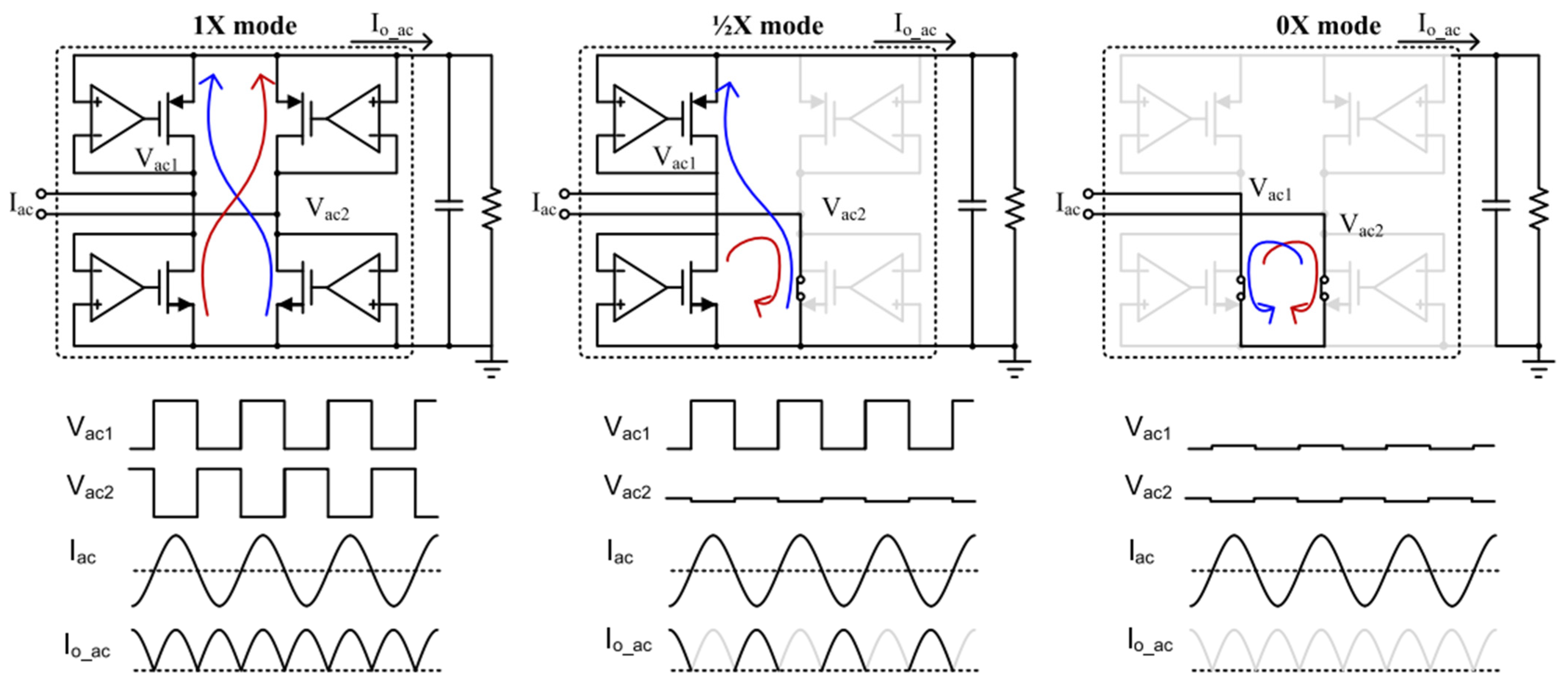
Ref. [70] reports a three-mode reconfigurable resonant regulating rectifier that integrates power conversion and voltage regulation into a single power stage. As shown in Figure 15, the rectifier can switch among 1X, 1/2X, and 0X modes. The 1X mode corresponds to full-wave rectification and provides the maximum output current Imax. The 1/2X mode corresponds to half-bridge rectification and provides approximately 1/2 Imax. The 0X mode is a freewheeling mode, in which the resonant current circulates inside the rectifier without delivering power to the output. By switching between the 1X and 1/2X modes under heavy-load conditions and between the 1/2X and 0X modes under light-load conditions, the average output current can be regulated over a wide load range, thereby achieving local voltage regulation at the RX side.
Compared with a simple 1X/0X two-mode scheme, the three-mode structure provides finer output-current resolution and distributes the delivered energy more evenly, thereby reducing the output voltage ripple. Its main contribution is that it extends the rectifier from a single power-conversion path into a multi-level power-regulation stage. Therefore, output voltage regulation no longer relies on an additional LDO or buck converter, but is realized through mode reconfiguration within the rectifier itself.
Building on this concept, hysteretic control and current-wave modulation (CWM) are further adopted in [71] for a series-resonant receiver. Compared with the three-mode structure, the five-level CWM scheme generates five equivalent output-current levels, namely 1X, 3/4X, 1/2X, 1/4X, and 0X, improving the resolution of average output-current regulation. As a result, the transferred power is distributed more uniformly in time, and the output voltage ripple is further reduced. In addition, the hysteretic controller allows the rectifier to switch rapidly to the required current level according to whether the output voltage crosses the hysteretic window, avoiding the response delay of conventional multicycle PWM control.
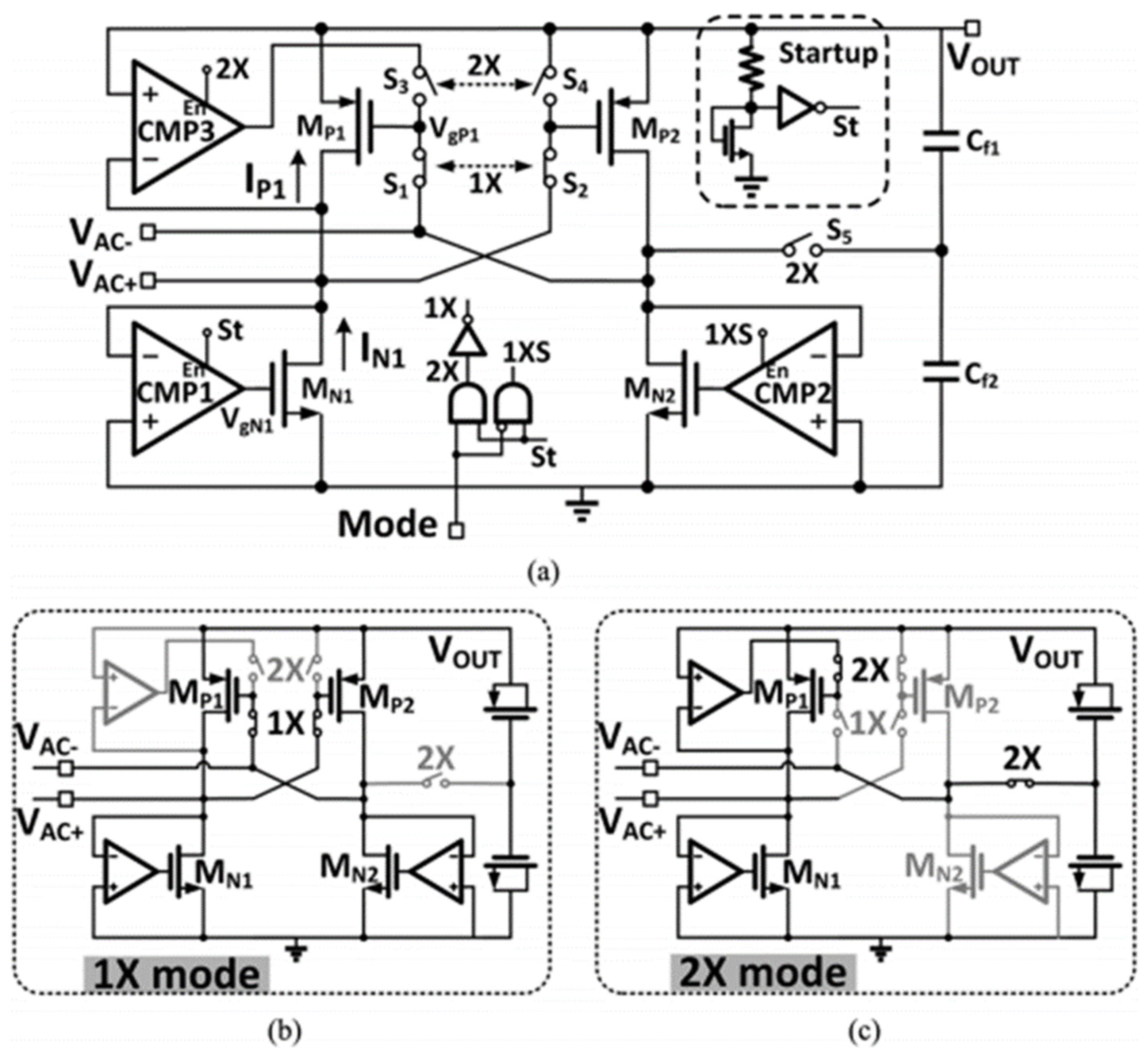
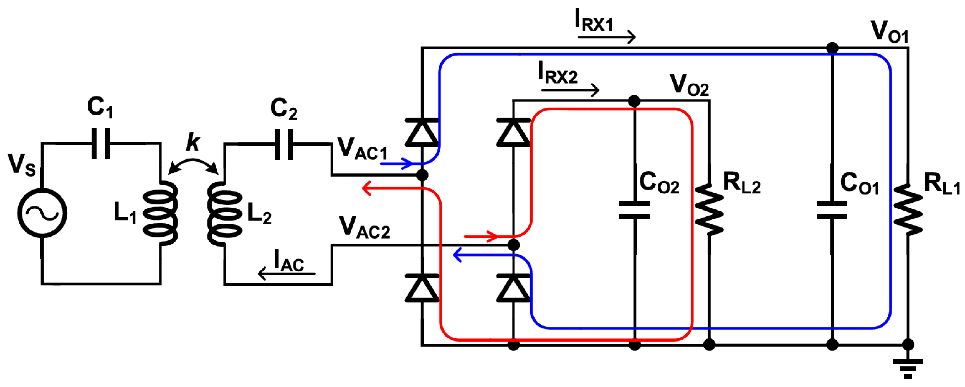
For a SP resonant network, the RX tank behaves more like a voltage-source-like input. Therefore, output voltage regulation is more suitably realized by changing the effective voltage conversion ratio of the rectifier. This principle is adopted in [72], where a 1X/2X reconfigurable resonant regulating rectifier is used for RX-side voltage regulation. As shown in Figure 16, The 1X mode corresponds to full-wave rectification, while the 2X mode corresponds to voltage-doubler rectification. By using an RX local PWM loop to control the duty ratio between these two modes within one modulation period, the output voltage can be regulated around the target value.
As the functions of wireless power receivers increase, a single output voltage is no longer sufficient for many systems. For example, portable and implantable devices often require both high-voltage and low-voltage power rails. A conventional solution first generates an unregulated DC voltage using a rectifier and then produces dual regulated outputs through an SIDO DC–DC converter or multiple post-stage regulators. However, this two-stage topology introduces additional power loss and increases the number of off-chip inductors and capacitors, as well as the system area. Therefore, single-stage dual-output regulating rectifiers have become an important direction for improving RX efficiency and integration.
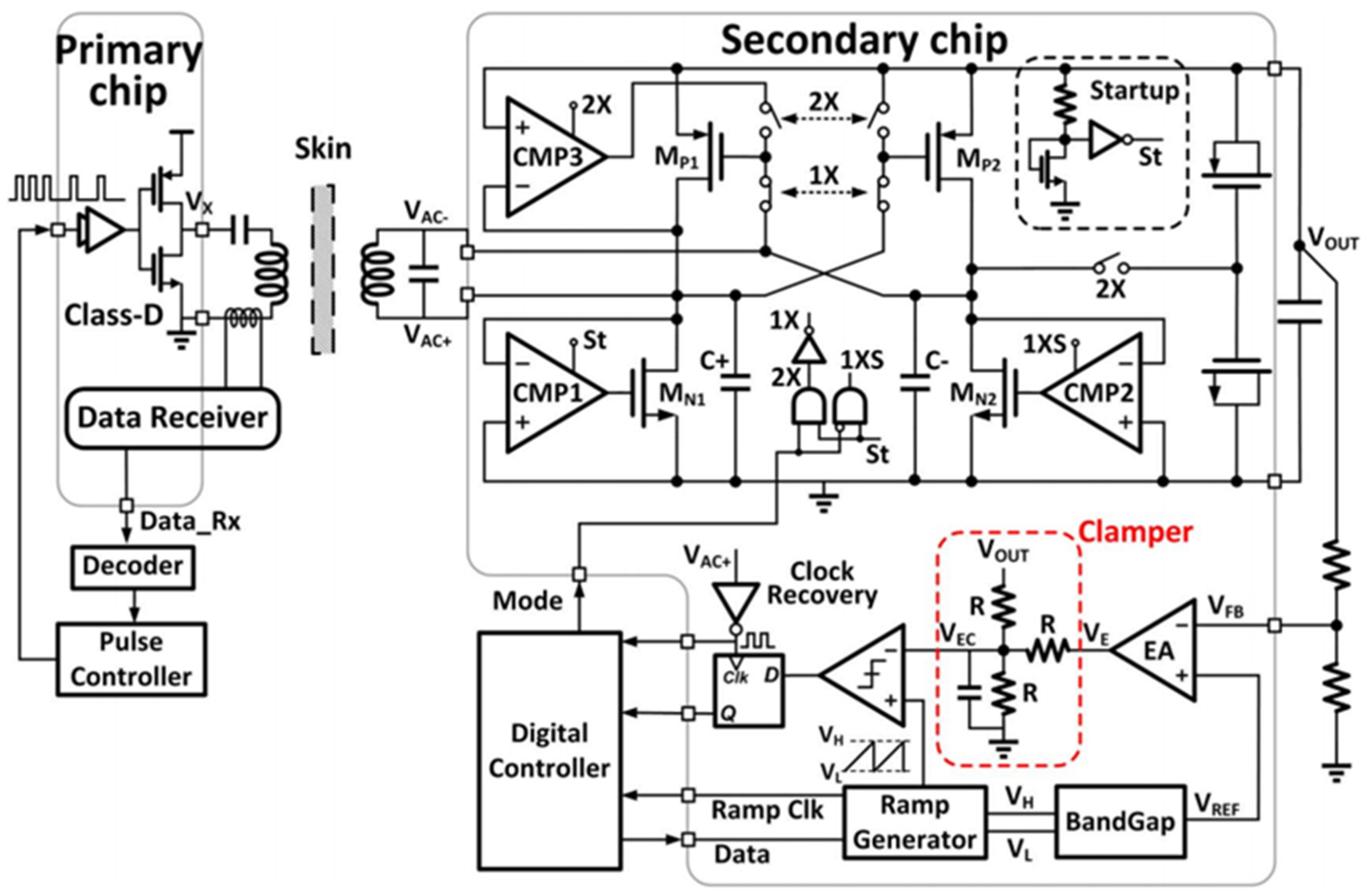
A 6.78-MHz single-stage dual-output regulating rectifier is reported in [73]. As shown in Figure 17, based on the current-source-like characteristic of the series-resonant RX tank, the positive and negative half cycles of the input AC current are assigned to two output nodes, respectively. Thus, AC–DC conversion and dual-output voltage regulation are achieved simultaneously in one rectifier. Each output employs an independent three-level CWM controller, which regulates its average output current by switching between the charging mode and the freewheeling mode. Since the two outputs receive energy from different current phases and are controlled independently, the cross-regulation problem commonly observed in dual-output systems can be effectively reduced.
For higher-frequency wireless powering, ref. [74] further presents a 40.68-MHz sin-gle-stage single-link, dual-output WPT system, which combines a resonant-current-mode receiver with coupling-adaptive regulation, demonstrating that high-frequency operation can support small receiver coils while maintaining power delivery under weak and vary-ing coupling conditions, as shown in Figure 18.
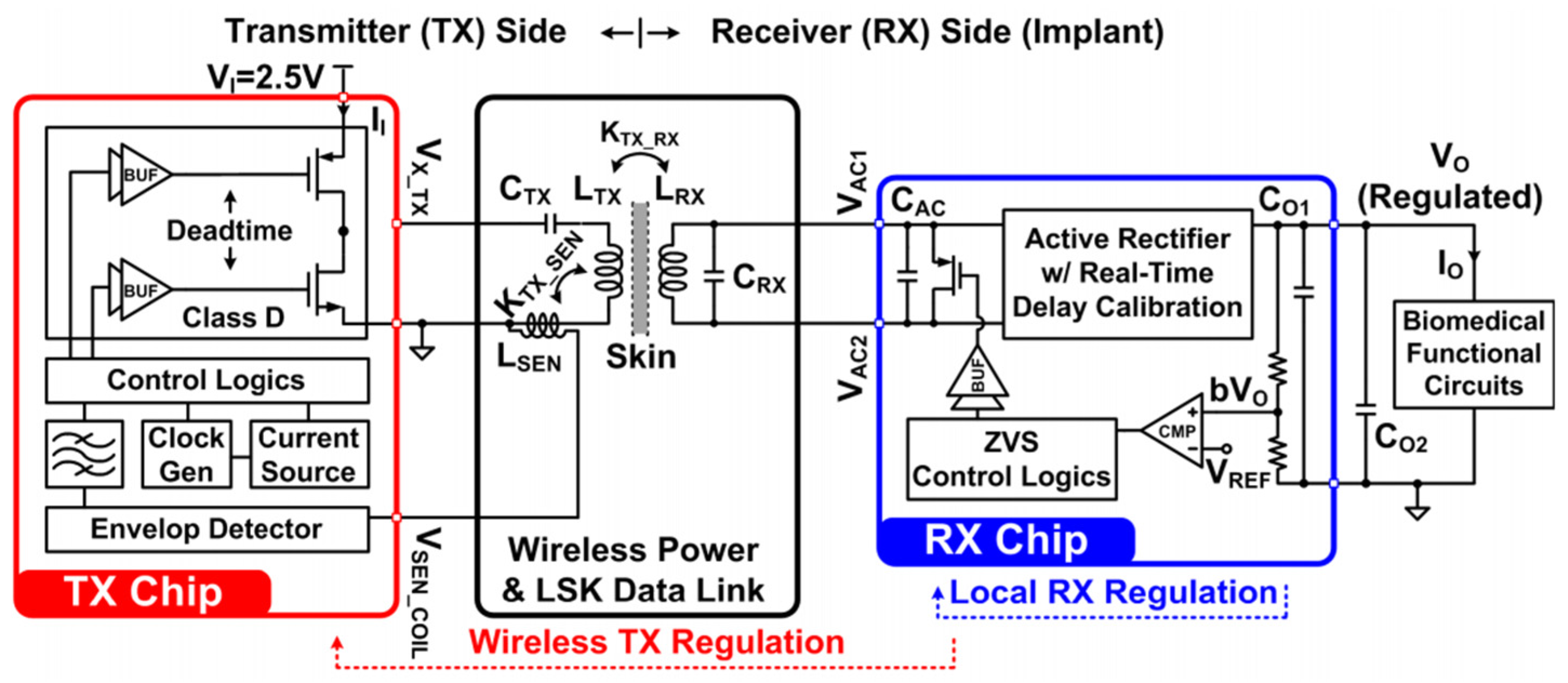
In addition to RX local voltage regulation, TX-side global power control isrequired to maintain high system efficiency and extend the operating range under dynamic load and coupling variations. When the transmitted power is higher than the RX power demand, excessive power degrades system efficiency and increases heat dissipation. Conversely, when the transmitted power is insufficient, the RX output voltage cannot be properly regulated. Coil misalignment further exacerbates this issue by causing substantial variations in the received power, which may result in output-voltage fluctuation or dropout. Although a local regulating rectifier can accommodate moderate input variations, its regulation range may be insufficient under severe weak-coupling conditions. Therefore, in a closed-loop TX–RX coordinated architecture, the RX local loop rapidly regulates the output, while the TX global loop uses receiver feedback to adjust the transmitted power or TX operating mode according to the RX voltage and power demand. Such coordination improves output-voltage regulation, avoids unnecessary power transmission under strong-coupling or light-load conditions, and reduces the power dissipated by receiver-side regulation [37].
Wireless power control based on load-shift keying (LSK) backscattering is a representative approach. The load variation at the RX side can be reflected to the TX side through the coupled coils, causing changes in the TX-side coil current or voltage envelope. Thus, the RX can feed back its power demand through load modulation, and the TX can adjust the transmitted power accordingly. In this way, a closed-loop system combining RX local voltage regulation and TX global power regulation can be established.
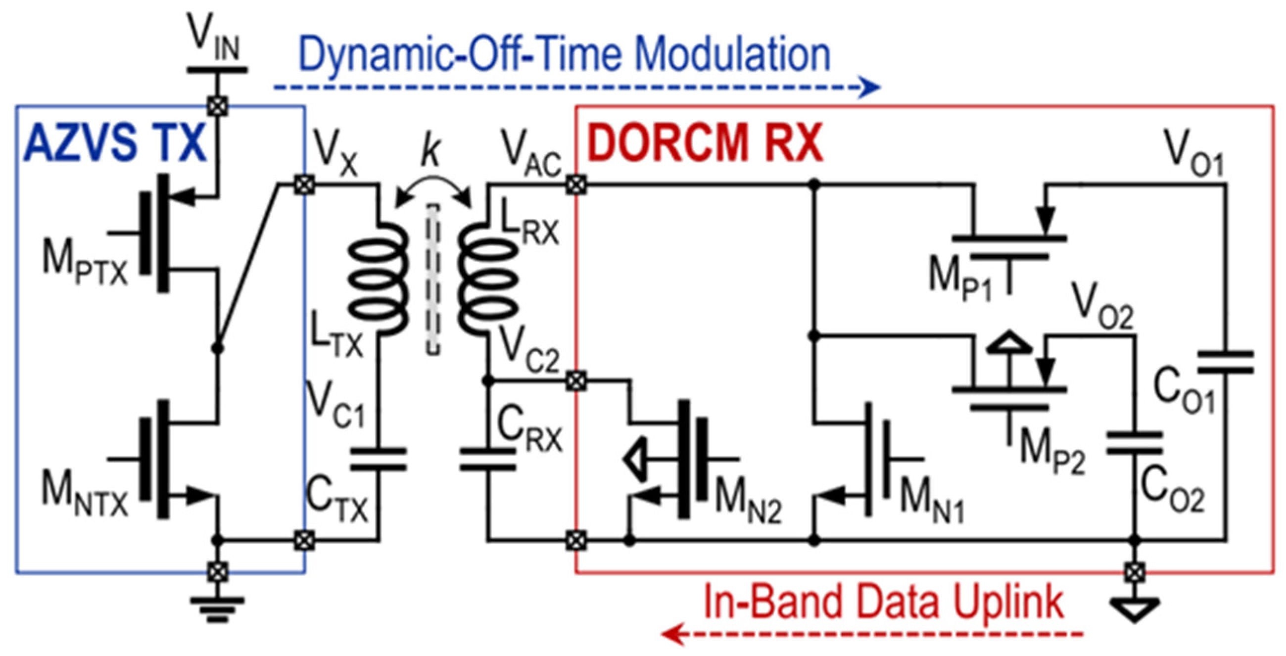
The work in [72] also extends the 1X/2X reconfigurable resonant regulating rectifier to a 13.56-MHz TX–RX jointly regulated WPT system for implantable medical devices. As shown in Figure 19, the RX local PWM loop controls the duty ratio between the 1X full-wave rectification mode and the 2X voltage-doubler mode to regulate the output voltage. Since the 1X/2X mode switching changes the equivalent input impedance of the RX and is reflected to the TX side through the coupled coils, the TX can detect the backscattered information using an additional detection coil, recover the RX mode-switching duty ratio, and adjust the transmitted power accordingly. This method combines RX local voltage regulation with TX global power control, allowing the system to maintain a regulated output under large load and coupling variations.
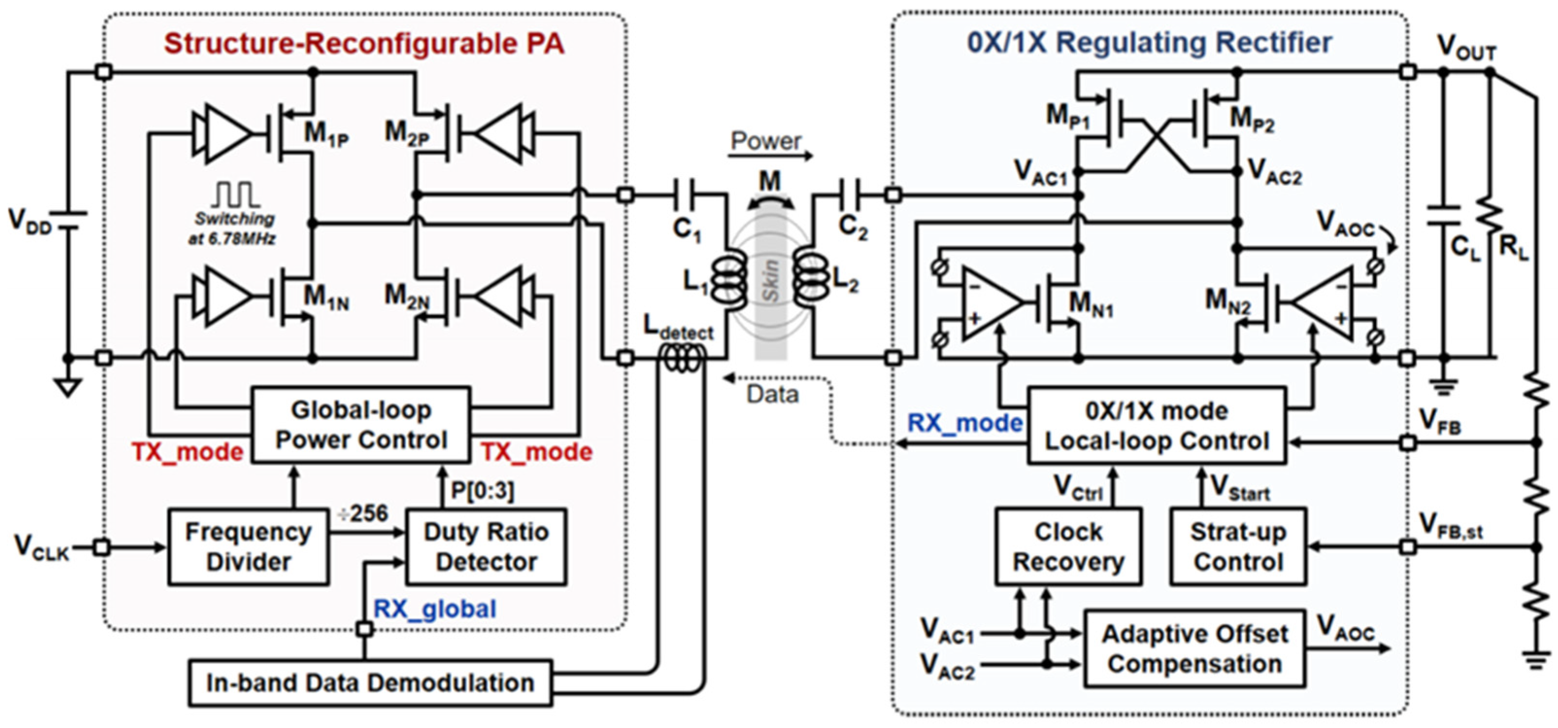
Another representative TX–RX coordinated regulation method is presented in [75], which consists of a structure-reconfigurable power amplifier (SR-PA) and a 0X/1X regulating rectifier. The architecture is shown in Figure 20, the RX achieves local voltage regulation through 0X/1X mode switching. The 1X mode delivers power to the load, whereas the 0X mode stops delivering power to the output, eliminating the need for a post-stage DC–DC converter. Since the 0X and 1X modes correspond to different RX input impedances, the mode switching produces load shift, which is reflected to the TX side through the wireless link. The TX recovers the feedback information using a detection coil and an in-band data demodulator, obtains the duty ratio of the RX 1X mode, and adjusts the operation time of the single mode and differential mode in the SR-PA accordingly. This structure reduces unnecessary power transmission from the TX side, thereby improving light-load efficiency and extending the available output power range.
Wireless constant-idle-time control is proposed in [76] to achieve RX local voltage regulation and TX global power regulation. When excessive received power is detected at the RX side, an on-chip switch shorts the RX AC input, producing load shift that is fed back to the TX through LSK backscattering. After recovering the feedback signal using an additional detection coil, the TX enters a fixed idle time and temporarily suspends power transmission to reduce the transmitted power. This nonlinear control method avoids the bandwidth limitation and complex compensation required by conventional linear control loops, enabling fast load-transient response and high system integration. The architecture is illustrated in Figure 21.
Following this approach, refs. [77,78] further develop a wireless hysteretic control technique. This method still uses the RX power state to generate LSK feedback, but replaces constant-idle-time control with hysteretic power regulation. When the RX output voltage reaches the upper boundary of the hysteretic window, the TX enters the low-power mode; when the output voltage falls to the lower boundary, the TX returns to the full-power mode. Compared with constant-idle-time control, hysteretic control adaptively adjusts the ratio between the TX full-power and low-power modes according to the load condition, reducing unnecessary power transmission under light-load conditions and improving end-to-end efficiency. The improved structure also eliminates the additional TX detection coil. Instead, an integrated current sensor directly detects the current variation in the Class-D driver to recover the LSK feedback signal, further improving system integration and reducing peripheral complexity.
In contrast to RX-initiated hysteretic regulation, recent studies have investigated primary-side hysteresis control for higher-power WPT systems. In [79], a TX-side hysteresis current controller was employed to force the primary current to track a composite reference formed by multiple frequency-specific command currents, thereby enabling flexible multifrequency and multiload power delivery, equivalent-current-source behavior, and power-factor improvement through a simple compensation capacitor. Building on this concept, ref. [80] proposed a primary-side dual-loop hysteresis controller for SS-compensated IPT systems, in which a narrow-band steady-state loop ensures accurate power regulation and suppresses power ripples, while a wide-band monitoring loop provides a rapid response to coupling and load disturbances. Since the high-bandwidth control relies mainly on locally measured primary-side power, it avoids the need for high-speed RX-to-TX communication and maintains ZVS over a wide operating range, making it particularly suitable for medium- and high-power applications requiring fast dynamic response and low power ripple.
However, compared with RX-initiated hysteretic regulation, primary-side hysteresis control eliminates high-speed wireless feedback and provides faster responses under coupling variations. However, it requires primary-side current or power sensing and is mainly suited to medium- and high-power IPT systems. In contrast, RX-initiated schemes remain more attractive for milliwatt-level biomedical implants because they directly regulate the implant supply voltage and can be integrated with the rectifier and load-modulation circuits.
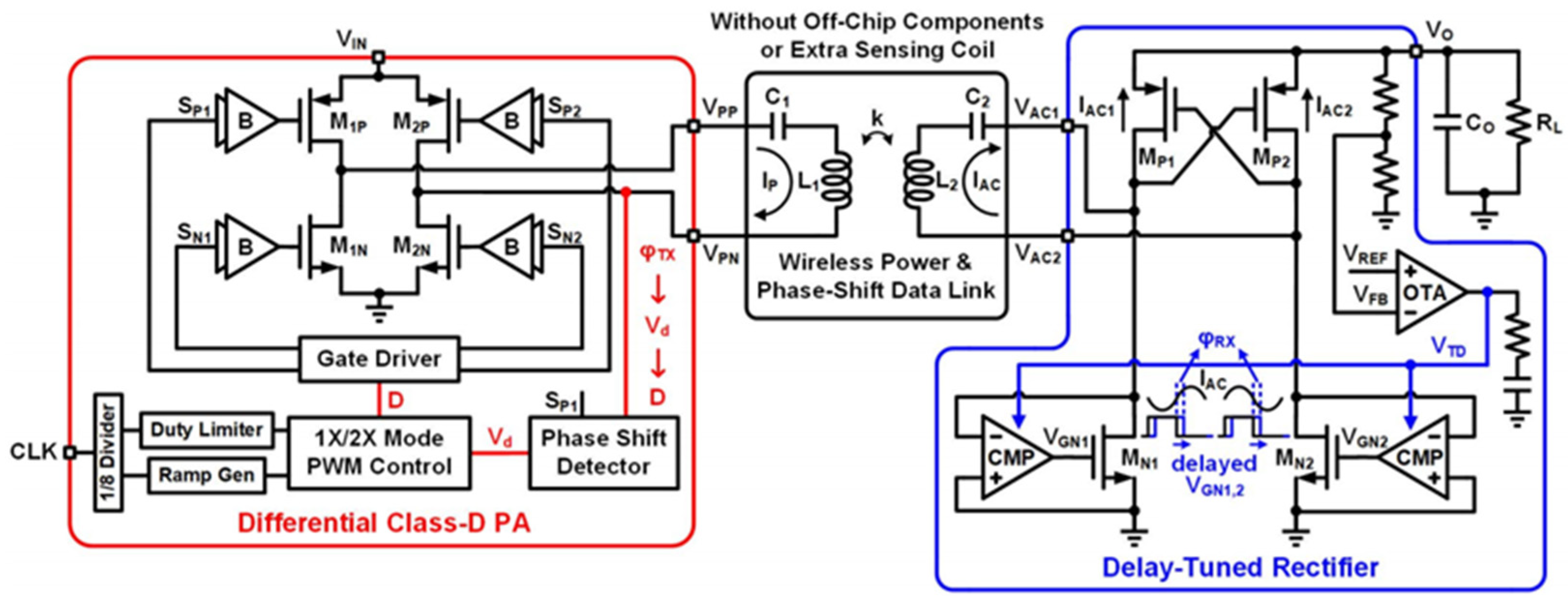
A different feedback mechanism is introduced in [81] through wireless phase shift control. As shown in Figure 22, the RX adopts a delay-tuned active rectifier, which adjusts the phase difference between the input current and input voltage by tuning the switching delay, thereby changing the average output current and achieving local voltage regulation. This phase difference contains information about the RX load and received power, and can be reflected to the TX side through the coupled link. Therefore, the TX no longer requires an additional detection coil or a backscattering data demodulator. Instead, a phase shift detector directly detects the phase difference between the TX-side voltage and current, based on which the duty ratio between the 1X and 2X operation modes of the Class-D PA is adjusted. This method provides a smoother feedback process without shorting the RX coil or introducing significant load disturbance, reducing the impact on the TX/RX AC current waveforms while improving system integration and end-to-end efficiency.

4.3.2. Comparison of Regulating Rectifier Techniques

As summarized in Table 3, regulating-rectifier architectures should first be selected according to the source characteristic of the resonant network. For SS receivers, the three-mode architecture in [70] and the five-level current-wave modulation (CWM) architecture in [71] regulate the average output current by switching among discrete current levels. The former supports 6 W with 92.2% peak RX efficiency and is suitable for high-current charging, but its coarse current resolution results in a 16-μs transient response and potentially larger output ripple. In contrast, ref. [71] uses five current levels and hysteretic selection to achieve an almost unnoticeable response to a 1:50 load change while maintaining 92.14% efficiency at 1.98 W, at the cost of increased switching and control complexity. For the voltage-source-like SP receiver, the 1X/2X structure in [72] changes the voltage conversion ratio and achieves 92.6% efficiency at 102 mW. It is therefore more suitable for miniaturized, high-impedance implants requiring voltage boosting, although it is more sensitive to received-voltage and coupling variations.
Dual-output architectures trade regulation flexibility for higher integration. The 6.78-MHz SS rectifier in [73] assigns different resonant-current phases to two independently controlled outputs and achieves 91.9% peak RX efficiency at 1.02 W. It eliminates post-stage multi-output converters and reduces cross-regulation, making it attractive for systems requiring separate analog and digital supplies. However, dividing the available current phases between the two outputs limits the independently deliverable power when their load demands are highly asymmetric. The 40.68-MHz system in [74] extends single-link dual-output operation to millimeter-scale implants and reports 90.1% peak RX efficiency. Its higher operating frequency facilitates receiver-coil miniaturization but increases switching, gate-driving, and timing-control losses. Therefore, single-stage dual-output rectifiers are preferable when compactness and conversion efficiency dominate, whereas post-regulation may still be required when low ripple, strong rail isolation, or widely unequal output powers are required.
TX–RX coordinated regulation improves robustness against load and coupling variations by reducing unnecessary transmitted power, but introduces additional sensing and control overhead. The SR-PA and 0X/1X rectifier in [75] achieve 92.9% peak RX efficiency and 71.5% end-to-end efficiency at 400 mW, providing favorable light-load performance at the cost of TX reconfiguration and feedback demodulation. Constant-idle-time control [76] provides a fast nonlinear response, while wireless hysteretic control [77,78] adaptively adjusts the TX power-state ratio; however, load shifting may disturb the resonant waveforms and increase output ripple. Primary-side hysteresis schemes [79,80] avoid high-speed RX-to-TX communication and are advantageous for high-power systems or rapidly varying coupling conditions, but they do not directly sense the implant voltage and require accurate TX-side current or power measurement. Phase-shift feedback [81] eliminates the additional sensing coil and backscattering demodulator and achieves 77% end-to-end efficiency with smoother link operation, although its accuracy depends on phase detection and rectifier timing. Therefore, RX-only regulation is generally preferable for simple milliwatt-level implants, whereas coordinated or primary-side control is more suitable when coupling tolerance, light-load efficiency, or fast dynamic response is the dominant requirement.
Beyond the topology-level trends summarized above, Table 3 also shows that high-performance regulating rectifiers have been implemented in mature CMOS and BCD technologies ranging from 0.65 to 0.18 μm. Moving to a smaller technology node can reduce the area of digital control circuits and improve timing resolution, benefiting adaptive delay compensation and calibration. However, it does not necessarily improve the power path because reduced supply and breakdown voltages, together with increased leakage and PVT sensitivity, may require thick-oxide or stacked devices. Therefore, the technology node should be selected according to the operating frequency, received power, voltage stress, and control complexity rather than chip area alone.
These process-level tradeoffs become particularly important when the reviewed architectures are applied to millimeter-scale implants. As the RX coil and available received power are reduced, circuit area, quiescent power, and control overhead become increasingly critical. Passive and cross-coupled rectifiers have relatively low overhead, whereas active rectifiers and adaptive delay compensation improve conversion efficiency at the cost of additional control circuitry. Single-stage regulating rectifiers and TX–RX coordinated control can reduce receiver-side conversion stages and unnecessary power dissipation. A recent 40.68-MHz system using an 8-mm RX coil and a 1.4-mm2 dual-output RX chip achieved a peak RX PCE of 90.3%, demonstrating millimeter-scale feasibility [74]. Further miniaturization remains limited by start-up and quiescent power, external components, and thermal constraints.

5. Conclusions

This review has summarized recent advances in integrated circuits for resonant WPT systems in biomedical implants, focusing on resonant compensation networks, active rectifiers, delay-compensation techniques, and regulating rectifiers. For implantable applications, the receiver must simultaneously provide high power-conversion efficiency, compact implementation, stable regulation, and reliable operation under coupling and load variations. Therefore, co-design of the resonant link, rectifier, regulator, and control circuits remains essential to overall system performance.
Among the available compensation networks, SS and SP topologies are generally more compatible with implantable receivers, while active rectifiers reduce forward-voltage loss and delay-compensation circuits suppress body-diode conduction and reverse current. However, existing studies still lack unified benchmarking across different topologies, operating frequencies, power levels, and CMOS processes. Control-circuit overhead, light-load efficiency, extreme weak-coupling behavior, and combined SAR–thermal performance are also insufficiently reported, making direct comparison and practical design selection difficult.
Future research should therefore move beyond peak PCE optimization toward safety- and robustness-oriented system design. Promising directions include low-overhead adaptive timing control, topology-reconfigurable receivers, coordinated TX–RX power regulation, multi-output single-stage conversion, automatic resonant tuning under coil displacement and detuning, artificial-intelligence-assisted power optimization, flexible and stretchable implantable electronics, and energy-aware power management. More comprehensive validation under PVT variations, realistic tissue environments, long-term implantation conditions, and standardized thermal and SAR constraints will be required to translate high-frequency, highly integrated WPT receivers from laboratory prototypes into reliable biomedical systems. Regulating rectifiers further improve receiver integration by combining AC–DC conversion and voltage regulation in a single stage. Recent designs show a clear trend from local RX regulation toward TX–RX coordinated power control and multi-output regulation. Overall, future implantable WPT receivers are expected to develop toward higher efficiency, smaller form factor, wider operating range, faster transient response, and stronger system-level adaptability.

Author Contributions

Conceptualization: J.F. and X.L.; data curation: J.F. and S.L.; draft preparation: J.F. and S.L.; writing, review and editing: J.F. and S.L.; formal analysis: all authors; supervision: X.L., J.F. and S.L. contribute equally to this work. All authors have read and agreed to the published version of the manuscript.

Funding

This research received no external funding.

Institutional Review Board Statement

Not applicable.

Informed Consent Statement

Not applicable.

Data Availability Statement

No new data were created or analyzed in this study. Data sharing is not applicable to this article.

Conflicts of Interest

The authors declare no conflict of interest.

References

  1. Galizzi, M.; Caldara, M.; Re, V.; Vitali, A. A novel Qi-standard compliant full-bridge wireless power charger for low power devices. In Proceedings of the 2013 IEEE Wireless Power Transfer (WPT), Perugia, Italy, 15–16 May 2013; pp. 44–47. [Google Scholar]
  2. Hwang, H.; Moon, J.; Lee, B.; Jeong, C.-H.; Kim, S.-W. An analysis of magnetic resonance coupling effects on wireless power transfer by coil inductance and placement. IEEE Trans. Consum. Electron. 2014, 60, 203–209. [Google Scholar] [CrossRef] [Scilit]
  3. Patil, D.; McDonough, M.K.; Miller, J.M.; Fahimi, B.; Balsara, P.T. Wireless Power Transfer for Vehicular Applications: Overview and Challenges. IEEE Trans. Transp. Electrif. 2018, 4, 3–37. [Google Scholar] [CrossRef] [Scilit]
  4. Covic, G.A.; Boys, J.T. Modern Trends in Inductive Power Transfer for Transportation Applications. IEEE J. Emerg. Sel. Top. Power Electron. 2013, 1, 28–41. [Google Scholar] [CrossRef] [Scilit]
  5. Wu, H.H.; Gilchrist, A.; Sealy, K.D.; Bronson, D. A High Efficiency 5 kW Inductive Charger for EVs Using Dual Side Control. IEEE Trans. Ind. Inform. 2012, 8, 585–595. [Google Scholar] [CrossRef] [Scilit]
  6. Tran, N.; Bai, S.; Yang, J.; Chun, H.; Kavehei, O.; Yang, Y.; Muktamath, V.; Ng, D.; Meffin, H.; Halpern, M.; et al. A Complete 256-Electrode Retinal Prosthesis Chip. IEEE J. Solid-State Circuits 2014, 49, 751–765. [Google Scholar] [CrossRef] [Scilit]
  7. Bhatti, P.T.; Wise, K.D. A 32-Site 4-Channel High-Density Electrode Array for a Cochlear Prosthesis. IEEE J. Solid-State Circuits 2006, 41, 2965–2973. [Google Scholar] [CrossRef] [Scilit]
  8. Lee, H.-M.; Park, H.; Ghovanloo, M. A Power-Efficient Wireless System With Adaptive Supply Control for Deep Brain Stimulation. IEEE J. Solid-State Circuits 2013, 48, 2203–2216. [Google Scholar] [CrossRef] [Scilit] [PubMed]
  9. Amar, A.B.; Kouki, A.B.; Cao, H. Power Approaches for Implantable Medical Devices. Sensors 2015, 15, 28889–28914. [Google Scholar] [CrossRef] [Scilit] [PubMed]
  10. Ballo, A.; Bottaro, M.; Grasso, A.D. A Review of Power Management Integrated Circuits for Ultrasound-Based Energy Harvesting in Implantable Medical Devices. Appl. Sci. 2021, 11, 2487. [Google Scholar] [CrossRef] [Scilit]
  11. Popovic, Z. Near- and far-field wireless power transfer. In Proceedings of the 2017 13th International Conference on Advanced Technologies, Systems and Services in Telecommunications (TELSIKS), Nis, Serbia, 18–20 October 2017; pp. 3–6. [Google Scholar]
  12. Schormans, M.; Valente, V.; Demosthenous, A. Practical Inductive Link Design for Biomedical Wireless Power Transfer: A Tutorial. IEEE Trans. Biomed. Circuits Syst. 2018, 12, 1112–1130. [Google Scholar] [CrossRef] [Scilit] [PubMed]
  13. Soltani, N.; ElAnsary, M.; Xu, J.; Filho, J.S.; Genov, R. Safety-Optimized Inductive Powering of Implantable Medical Devices: Tutorial and Comprehensive Design Guide. IEEE Trans. Biomed. Circuits Syst. 2021, 15, 1354–1367. [Google Scholar] [CrossRef] [Scilit] [PubMed]
  14. Ahn, D.; Ghovanloo, M. Optimal Design of Wireless Power Transmission Links for Millimeter-Sized Biomedical Implants. IEEE Trans. Biomed. Circuits Syst. 2016, 10, 125–137. [Google Scholar] [CrossRef] [Scilit] [PubMed]
  15. Hui, S.Y.R.; Zhong, W.; Lee, C.K. A Critical Review of Recent Progress in Mid-Range Wireless Power Transfer. IEEE Trans. Power Electron. 2014, 29, 4500–4511. [Google Scholar] [CrossRef] [Scilit]
  16. Cannon, B.L.; Hoburg, J.F.; Stancil, D.D.; Goldstein, S.C. Magnetic Resonant Coupling As a Potential Means for Wireless Power Transfer to Multiple Small Receivers. IEEE Trans. Power Electron. 2009, 24, 1819–1825. [Google Scholar] [CrossRef] [Scilit]
  17. Liu, C.; Guo, Y.-X.; Sun, H.; Xiao, S. Design and Safety Considerations of an Implantable Rectenna for Far-Field Wireless Power Transfer. IEEE Trans. Antennas Propag. 2014, 62, 5798–5806. [Google Scholar] [CrossRef] [Scilit]
  18. Ding, S.; Koulouridis, S.; Pichon, L. Implantable Wireless Transmission Rectenna System for Biomedical Wireless Applications. IEEE Access 2020, 8, 195551–195558. [Google Scholar] [CrossRef] [Scilit]
  19. Basir, A.; Yoo, H. Efficient Wireless Power Transfer System With a Miniaturized Quad-Band Implantable Antenna for Deep-Body Multitasking Implants. IEEE Trans. Microw. Theory Tech. 2020, 68, 1943–1953. [Google Scholar] [CrossRef] [Scilit]
  20. Saha, N.; Kakaraparty, K.; Pineda, E.A.; Mahbub, I. Wireless Powering of Implants and Wearables: Challenges (and opportunities) toward transitioning from bench-top to clinical studies [Bioelectromagnetics]. IEEE Antennas Propag. Mag. 2025, 67, 59–71. [Google Scholar] [CrossRef] [Scilit]
  21. Zahid, Z.U.; Zheng, C.; Chen, R.; Faraci, W.E.; Lai, J.-S.J.; Senesky, M.; Anderson, D. Design and control of a single-stage large air-gapped transformer isolated battery charger for wide-range output voltage for EV applications. In Proceedings of the 2013 IEEE Energy Conversion Congress and Exposition, Denver, CO, USA, 15–19 September 2013; pp. 5481–5487. [Google Scholar]
  22. Li, H.; Li, J.; Wang, K.; Chen, W.; Yang, X. A Maximum Efficiency Point Tracking Control Scheme for Wireless Power Transfer Systems Using Magnetic Resonant Coupling. IEEE Trans. Power Electron. 2015, 30, 3998–4008. [Google Scholar] [CrossRef] [Scilit]
  23. Wang, C.-S.; Stielau, O.H.; Covic, G.A. Design considerations for a contactless electric vehicle battery charger. IEEE Trans. Ind. Electron. 2005, 52, 1308–1314. [Google Scholar] [CrossRef] [Scilit]
  24. Mai, J.; Yang, A.; Liu, Z.; Wang, Y.; Zhang, B.; Xu, D. A Segmented Parallel S/S Compensation Topology and Its Harmonic Suppression Method for IPT System. IEEE J. Emerg. Sel. Top. Power Electron. 2025, 13, 4315–4325. [Google Scholar] [CrossRef] [Scilit]
  25. Kim, S.; Park, H.-H.; Kim, J.; Kim, J.; Ahn, S. Design and Analysis of a Resonant Reactive Shield for a Wireless Power Electric Vehicle. IEEE Trans. Microw. Theory Tech. 2014, 62, 1057–1066. [Google Scholar] [CrossRef] [Scilit]
  26. Choi, S.Y.; Gu, B.W.; Lee, S.W.; Lee, W.Y.; Huh, J.; Rim, C.T. Generalized Active EMF Cancel Methods for Wireless Electric Vehicles. IEEE Trans. Power Electron. 2014, 29, 5770–5783. [Google Scholar] [CrossRef] [Scilit]
  27. Liu, C.; Guan, Y.; Yao, T.; Wang, Y.; Xu, D. Multi Module Parallel MHz Power Amplifier with Hybrid Structure and Optimized Control Strategy. IEEE Trans. Power Electron. 2025, 40, 7994–8004. [Google Scholar] [CrossRef] [Scilit]
  28. Khaligh, A.; Dusmez, S. Comprehensive Topological Analysis of Conductive and Inductive Charging Solutions for Plug-In Electric Vehicles. IEEE Trans. Veh. Technol. 2012, 61, 3475–3489. [Google Scholar] [CrossRef] [Scilit]
  29. Aditya, K.; Williamson, S.S. Design considerations for loosely coupled inductive power transfer (IPT) system for electric vehicle battery charging-A comprehensive review. In Proceedings of the 2014 IEEE Transportation Electrification Conference and Expo (ITEC), Dearborn, MI, USA, 15–18 June 2014; pp. 1–6. [Google Scholar]
  30. Mude, K.N.; Aditya, K. Comprehensive review and analysis of two-element resonant compensation topologies for wireless inductive power transfer systems. Chin. J. Electr. Eng. 2019, 5, 14–31. [Google Scholar] [CrossRef] [Scilit]
  31. Lu, Y.; Yang, B.; He, S.; Peng, Y.; Lyu, T.; Mai, R.; Chen, Y. Design of Compensation Topology for IPT System Considering Coils’ Parameters and Load Variations for CC or CV Output. IEEE Trans. Transp. Electrif. 2024, 10, 1583–1595. [Google Scholar] [CrossRef] [Scilit]
  32. Basir, A.; Shah, I.A.; Yoo, H. Sphere-Shaped Implantable Receiver Coil for Misalignment-Resilient Wireless Power Transfer Systems for Implantable Devices. IEEE Trans. Antennas Propag. 2022, 70, 8368–8378. [Google Scholar] [CrossRef] [Scilit]
  33. Meng, X.; Li, X.; Tsui, C.-Y.; Ki, W.-H.; Liu, W. A 13.56-MHz Primary Driver With Fractional Capacitance Auto-Tuning Loop for Wireless-Powered Implantable Medi-cal Devices. IEEE J. Solid-State Circuits 2024, 59, 3218–3231. [Google Scholar] [CrossRef] [Scilit]
  34. Barbruni, G.L.; Cordara, C.; Carminati, M.; Carrara, S.; Ghezzi, D. A Fre-quency-Switching Inductive Power Transfer System for Wireless, Miniaturised and Large-Scale Neural Interfaces. IEEE Trans. Biomed. Circuits Syst. 2024, 18, 679–690. [Google Scholar] [CrossRef] [Scilit] [PubMed]
  35. Zhu, H.; Wu, X.; Xiong, F.; Tahir, M. Robust Wireless Power and Data Transmission System Against Misalignment for Implantable Medical Devices. IEEE Trans. Power Electron. 2025, 40, 14169–14180. [Google Scholar] [CrossRef] [Scilit]
  36. Karimi, M.J.; Jin, M.; Dehollain, C.; Schmid, A. A Wireless Power Conver-sion Chain With Fully On-Chip Automatic Resonance Tuning System for Biomedical Im-plants. IEEE Open J. Circuits Syst. 2024, 5, 117–127. [Google Scholar] [CrossRef] [Scilit]
  37. Lu, T.; Du, S. A Coupling-Adaptive Wireless Power Transfer System With Voltage-/Current-Mode Receiver and Global Digital-PWM Regulation. IEEE J. Solid-State Circuits 2024, 59, 4175–4187. [Google Scholar] [CrossRef] [Scilit]
  38. Pahlavan, S.; Shooshtari, M.; Jafarabadi Ashtiani, S. Star-Shaped Coils in the Transmitter Array for Receiver Rotation Tolerance in Free-Moving Wireless Power Transfer Applications. Energies 2022, 15, 8643. [Google Scholar] [CrossRef] [Scilit]
  39. Ahn, J.; Woo, S.; Kim, H.; Song, K.; Huh, S.; Hong, S.-E.; Kim, J.; Choi, H.-D.; Ahn, S. An Out-of-Phase Wireless Power Transfer System for Implantable Medical Devices to Reduce Human Exposure to Electromagnetic Field and Increase Power Transfer Efficiency. IEEE Trans. Biomed. Circuits Syst. 2022, 16, 1166–1180. [Google Scholar] [CrossRef] [Scilit] [PubMed]
  40. Lyu, H.; Babakhani, A. A 13.56-MHz −25-dBm-Sensitivity Inductive Power Receiver System-on-a-Chip With a Successive-Approximation Resonance Compensation Front-End for Ultra-Low-Power Medical Implants. IEEE Trans. Biomed. Circuits Syst. 2021, 15, 80–90. [Google Scholar] [CrossRef] [Scilit] [PubMed]
  41. Rodriguez-Fuentes, A.; Jimenez Carrizosa, M.; Ramos, R. Neural Network-Based Design of Wireless Power Transfer Systems for Implantable Medical Devices. IEEE Trans. Power Electron. 2026, 41, 3011–3024. [Google Scholar] [CrossRef] [Scilit]
  42. Alonzo, J.; Daling, M.H.; Lee, J.; Lee, A.-H.; Durfee, D.; Asbeck, P.; Larson, L.; Nurmikko, A.; Leung, V.W. Analysis of Wireless Power Transfer Efficiency and Specific Absorption Rate for a Distributed Brain Implant System. In Proceedings of the 2024 IEEE 20th International Conference on Body Sensor Networks (BSN), Chicago, IL, USA, 15–17 October 2024; pp. 1–4. [Google Scholar]
  43. ISO 14708-1:2014; Implants for Surgery—Active Implantable Medical Devices—Part 1: General Requirements for Safety, Marking and for Information to Be Provided by the Manufacturer. International Organization for Standardization: Geneva, Switzerland, 2014.
  44. Xia, F.; Mao, F.; Lu, Y.; Sawan, M. Optimizing Power Transfer Efficiency in Biomedical Implants: A Comparative Analysis of SS and SP Inductive Link Topologies. IEEE Trans. Power Electron. 2024, 39, 11770–11783. [Google Scholar] [CrossRef] [Scilit]
  45. Al-Kalbani, A.I.; Yuce, M.R.; Redouté, J.-M. A Biosafety Comparison Between Capacitive and Inductive Coupling in Biomedical Implants. IEEE Antennas Wirel. Propag. Lett. 2014, 13, 1168–1171. [Google Scholar] [CrossRef] [Scilit]
  46. Yeon, P.; Mirbozorgi, S.A.; Lim, J.; Ghovanloo, M. Feasibility Study on Active Back Telemetry and Power Transmission Through an Inductive Link for Millimeter-Sized Biomedical Implants. IEEE Trans. Biomed. Circuits Syst. 2017, 11, 1366–1376. [Google Scholar] [CrossRef] [Scilit] [PubMed]
  47. Cao, X.; Sato, H.; Xu, K.-D.; Jiang, W.; Gong, S.; Chen, Q. A Systematic Method for Efficient Wireless Powering to Implantable Biomedical Devices. IEEE Trans. Antennas Propag. 2023, 71, 2745–2757. [Google Scholar] [CrossRef] [Scilit]
  48. Ballo, A.; Grasso, A.D.; Palumbo, G. A Review of Charge Pump Topologies for the Power Management of IoT Nodes. Electronics 2019, 8, 480. [Google Scholar] [CrossRef] [Scilit]
  49. Guo, S.; Lee, H. An Efficiency-Enhanced CMOS Rectifier with Unbalanced-Biased Comparators for Transcutaneous-Powered High-Current Implants. IEEE J. Solid-State Circuits 2009, 44, 1796–1804. [Google Scholar] [CrossRef] [Scilit]
  50. Lam, Y.-H.; Ki, W.-H.; Tsui, C.-Y. Integrated Low-Loss CMOS Active Rectifier for Wirelessly Powered Devices. IEEE Trans. Circuits Syst. II Express Briefs 2006, 53, 1378–1382. [Google Scholar] [CrossRef] [Scilit]
  51. Cha, H.-K.; Park, W.-T.; Je, M. A CMOS Rectifier With a Cross-Coupled Latched Comparator for Wireless Power Transfer in Biomedical Applications. IEEE Trans. Circuits Syst. II Express Briefs 2012, 59, 409–413. [Google Scholar] [CrossRef] [Scilit]
  52. Lu, Y.; Ki, W.-H. A 13.56 MHz CMOS Active Rectifier With Switched-Offset and Compensated Biasing for Biomedical Wireless Power Transfer Systems. IEEE Trans. Biomed. Circuits Syst. 2014, 8, 334–344. [Google Scholar] [CrossRef] [Scilit] [PubMed]
  53. Lee, H.-M.; Ghovanloo, M. An Integrated Power-Efficient Active Rectifier With Offset-Controlled High Speed Comparators for Inductively Powered Applications. IEEE Trans. Circuits Syst. I Regul. Pap. 2011, 58, 1749–1760. [Google Scholar] [CrossRef] [Scilit] [PubMed]
  54. Qian, X.-H.; Cheng, M.-S.; Wu, C.-Y. A CMOS 13.56-MHz high-efficiency low-dropout-voltage 40-mW inductive link power supply utilizing on-chip delay-compensated voltage doubler rectifier and multiple LDOs for implantable medical devices. In Proceedings of the 2013 IEEE Asian Solid-State Circuits Conference (A-SSCC), Singapore, 11–13 November 2013; pp. 257–260. [Google Scholar]
  55. Chung, H.; Radecki, A.; Miura, N.; Ishikuro, H.; Kuroda, T. A 0.025–0.45 W 60–Efficiency Inductive-Coupling Power Transceiver With 5-Bit Dual-Frequency Feedforward Control for Non-Contact Memory Cards. IEEE J. Solid-State Circuits 2012, 47, 2496–2504. [Google Scholar] [CrossRef] [Scilit]
  56. Hashemi, S.S.; Sawan, M.; Savaria, Y. A High-Efficiency Low-Voltage CMOS Rectifier for Harvesting Energy in Implantable Devices. IEEE Trans. Biomed. Circuits Syst. 2012, 6, 326–335. [Google Scholar] [CrossRef] [Scilit] [PubMed]
  57. Cheng, L.; Ki, W.-H.; Lu, Y.; Yim, T.-S. Adaptive On/Off Delay-Compensated Active Rectifiers for Wireless Power Transfer Systems. IEEE J. Solid-State Circuits 2016, 51, 712–723. [Google Scholar] [CrossRef] [Scilit]
  58. Huang, C.; Kawajiri, T.; Ishikuro, H. A Near-Optimum 13.56 MHz CMOS Active Rectifier With Circuit-Delay Real-Time Calibrations for High-Current Biomedical Implants. IEEE J. Solid-State Circuits 2016, 51, 1797–1809. [Google Scholar] [CrossRef] [Scilit]
  59. Noh, K.; Amanor-Boadu, J.; Zhang, M.; Sánchez-Sinencio, E. A 13.56-MHz CMOS Active Rectifier With a Voltage Mode Switched-Offset Comparator for Implantable Medical Devices. IEEE Trans. Very Large Scale Integr. (VLSI) Syst. 2018, 26, 2050–2060. [Google Scholar] [CrossRef] [Scilit]
  60. Xue, Z.; Fan, S.; Li, D.; Zhang, L.; Gou, W.; Geng, L. A 13.56 MHz, 94.1% Peak Efficiency CMOS Active Rectifier With Adaptive Delay Time Control for Wireless Power Transmission Systems. IEEE J. Solid-State Circuits 2019, 54, 1744–1754. [Google Scholar] [CrossRef] [Scilit]
  61. Erfani, R.; Marefat, F.; Nag, S.; Mohseni, P. A 1–10-MHz Frequency-Aware CMOS Active Rectifier With Dual-Loop Adaptive Delay Compensation. IEEE J. Solid-State Circuits 2020, 55, 756–766. [Google Scholar] [CrossRef]
  62. Cheng, L.; Ge, X.; Hu, L.; Yao, Y.; Ki, W.-H.; Tsui, C.-Y. A 40.68-MHz Active Rectifier With Hybrid Adaptive On/Off Delay-Compensation Scheme for Biomedical Implantable Devices. IEEE Trans. Circuits Syst. I Regul. Pap. 2020, 67, 516–525. [Google Scholar] [CrossRef] [Scilit]
  63. Luo, Z.; Liu, J.; Lee, H. A 40.68-MHz Active Rectifier with Cycle-Based On-/Off-Delay Compensation for High-Current Biomedical Implants. IEEE J. Solid-State Circuits 2023, 58, 345–356. [Google Scholar] [CrossRef] [Scilit]
  64. Wu, C.-Y.; Qian, X.-H.; Cheng, M.-S.; Liang, Y.-A.; Chen, W.-M. A 13.56 MHz 40 mW CMOS High-Efficiency Inductive Link Power Supply Utilizing On-Chip Delay-Compensated Voltage Doubler Rectifier and Multiple LDOs for Implantable Medical Devices. IEEE J. Solid-State Circuits 2014, 49, 2397–2407. [Google Scholar] [CrossRef] [Scilit]
  65. Kiani, M.; Lee, B.; Yeon, P.; Ghovanloo, M. A Q-Modulation Technique for Efficient Inductive Power Transmission. IEEE J. Solid-State Circuits 2015, 50, 2839–2848. [Google Scholar] [CrossRef] [Scilit] [PubMed]
  66. Moon, Y.-J.; Roh, Y.-S.; Yoo, C.; Kim, D.-Z. A 3.0-W wireless power receiver circuit with 75-% overall efficiency. In Proceedings of the 2012 IEEE Asian Solid State Circuits Conference (A-SSCC), Kobe, Japan, 12–14 November 2012; pp. 97–100. [Google Scholar]
  67. Moh, K.-G.; Neri, F.; Moon, S.; Yeon, P.; Yu, J.; Cheon, Y.; Roh, Y.-S.; Ko, M.; Park, B.-H. 12.9 A fully integrated 6W wireless power receiver operating at 6.78MHz with magnetic resonance coupling. In Proceedings of the 2015 IEEE International Solid-State Circuits Conference-(ISSCC) Digest of Technical Papers, San Francisco, CA, USA, 22–26 February 2015; pp. 1–3. [Google Scholar]
  68. Riehl, P.S.; Satyamoorthy, A.; Akram, H.; Yen, Y.-C.; Yang, J.-C.; Juan, B.; Lee, C.-M.; Lin, F.-C.; Muratov, V.; Plumb, W.; et al. Wireless Power Systems for Mobile Devices Supporting Inductive and Resonant Operating Modes. IEEE Trans. Microw. Theory Tech. 2015, 63, 780–790. [Google Scholar] [CrossRef] [Scilit]
  69. Park, H.-G.; Jang, J.-H.; Kim, H.-J.; Park, Y.-J.; Oh, S.; Pu, Y.; Hwang, K.C.; Yang, Y.; Lee, K.-Y. A Design of a Wireless Power Receiving Unit With a High-Efficiency 6.78-MHz Active Rectifier Using Shared DLLs for Magnetic-Resonant A4 WP Applications. IEEE Trans. Power Electron. 2016, 31, 4484–4498. [Google Scholar] [CrossRef] [Scilit]
  70. Cheng, L.; Ki, W.-H.; Tsui, C.-Y. A 6.78-MHz Single-Stage Wireless Power Receiver Using a 3-Mode Reconfigurable Resonant Regulating Rectifier. IEEE J. Solid-State Circuits 2017, 52, 1412–1423. [Google Scholar] [CrossRef] [Scilit]
  71. Lin, J.; Zhan, C.; Lu, Y. A 6.78-MHz Single-Stage Wireless Power Receiver With Ultrafast Transient Response Using Hysteretic Control and Multilevel Current-Wave Modulation. IEEE Trans. Power Electron. 2021, 36, 9918–9926. [Google Scholar] [CrossRef] [Scilit]
  72. Li, X.; Tsui, C.-Y.; Ki, W.-H. A 13.56 MHz Wireless Power Transfer System With Reconfigurable Resonant Regulating Rectifier and Wireless Power Control for Implantable Medical Devices. IEEE J. Solid-State Circuits 2015, 50, 978–989. [Google Scholar] [CrossRef] [Scilit]
  73. Lin, J.; Lu, Y.; Zhan, C.; Martins, R.P. A Single-Stage Dual-Output Regulating Rectifier With Hysteretic Current-Wave Modulation. IEEE J. Solid-State Circuits 2021, 56, 2770–2780. [Google Scholar] [CrossRef] [Scilit]
  74. Lu, T.; Du, S. A 40.68-MHz Dual-Output Wireless Power Transfer System for Milli-meter-Scale Biomedical Implants. IEEE J. Solid-State Circuits 2026, 61, 963–976. [Google Scholar] [CrossRef] [Scilit]
  75. Yang, F.-B.; Fuh, J.; Li, Y.-H.; Takamiya, M.; Chen, P.-H. Structure-Reconfigurable Power Amplifier (SR-PA) and 0X/1X Regulating Rectifier for Adaptive Power Control in Wireless Power Transfer System. IEEE J. Solid-State Circuits 2021, 56, 2054–2064. [Google Scholar] [CrossRef] [Scilit]
  76. Huang, C.; Kawajiri, T.; Ishikuro, H. A wireless power transfer system with enhanced response and efficiency by fully-integrated fast-tracking wireless constant-idle-time control for implants. In Proceedings of the 2016 IEEE Symposium on VLSI Circuits (VLSI-Circuits), Honolulu, HI, USA, 15–17 June 2016; pp. 1–2. [Google Scholar]
  77. Tang, J.; Zhao, L.; Huang, C. 33.6 A Wireless Power Transfer System with Up-to-20% Light- Load Efficiency Enhancement and Instant Dynamic Response by Fully Integrated Wireless Hysteretic Control for Bioimplants. In Proceedings of the 2021 IEEE International Solid-State Circuits Conference (ISSCC), San Francisco, CA, USA, 13–22 February 2021; pp. 470–472. [Google Scholar]
  78. Tang, J.; Zhao, L.; Huang, C. A Wireless Hysteretic Controlled Wireless Power Transfer System with Enhanced Efficiency and Dynamic Response for Bioimplants. IEEE J. Solid-State Circuits 2023, 58, 1160–1171. [Google Scholar] [CrossRef] [Scilit]
  79. Sun, A.; Xia, C.; Chen, Y.; Liu, Y.; Yang, Z.; Zhao, S.; Yang, Z. Multifrequency and Multiload MCR-WPT System Based on Hysteresis Current Control. IEEE Trans. Power Electron. 2024, 39, 10532–10545. [Google Scholar] [CrossRef] [Scilit]
  80. Zhou, J.; Guidi, G.; Chen, S.; Tang, Y.; Suul, J.A. Primary-Side Dual-Loop Hysteresis Control for Fast Dynamic Response and Low Power Ripples in Inductive Power Transfer Systems. IEEE J. Emerg. Sel. Top. Power Electron. 2026, 14, 1362–1374. [Google Scholar] [CrossRef] [Scilit]
  81. Bai, X.; Lu, Y.; Zhan, C.; Martins, R.P. A 6.78-MHz Wireless Power Transfer System With Inherent Wireless Phase Shift Control Without Feedback Data Sensing Coil. IEEE J. Solid-State Circuits 2023, 58, 1746–1757. [Google Scholar] [CrossRef] [Scilit]
Figure 1. Typical Architecture of Biomedical Implants.
Electronics 15 03723 g001
Figure 2. Schematic illustrations of different WPT modalities.
Electronics 15 03723 g002
Figure 3. Typical architecture of a resonant WPT system.
Electronics 15 03723 g003
Figure 4. Four Primary Compensation Topologies.
Electronics 15 03723 g004
Figure 5. Schematic of different rectifiers (a) Half-bridge rectifier. (b) Full-bridge rectifier.
Electronics 15 03723 g005
Figure 6. Cross-coupled rectifier.
Electronics 15 03723 g006
Figure 7. Active full-wave rectifier [49].
Electronics 15 03723 g007
Figure 8. Waveforms of active rectifiers.
Electronics 15 03723 g008
Figure 9. Schematic of the active diode with the adaptive on/off delay-compensation technique [57].
Electronics 15 03723 g009
Figure 10. The delay compensation technique in [59]. (a) Simplified nMOS active diode. (b) its detailed VDS sampling network.
Electronics 15 03723 g010
Figure 11. The current controlled delay line technique [60].
Electronics 15 03723 g011
Figure 12. System architecture of the dual-loop adaptive delay compensation rectifier [61].
Electronics 15 03723 g012
Figure 13. Schematic of the active rectifier with the active diode using hybrid compensation scheme [62].
Electronics 15 03723 g013
Figure 14. The cycle-based on/off-delay compensation technique [63].
Electronics 15 03723 g014
Figure 15. The three-mode reconfigurable resonant regulating rectifier [70].
Electronics 15 03723 g015
Figure 16. (a) 1X/2X reconfigurable rectifier; (b) 1X mode; (c) 2X mode [72].
Electronics 15 03723 g016
Figure 17. Dual-output rectifier proposed in [73].
Electronics 15 03723 g017
Figure 18. Structure of the proposed 40.68-MHz WPT system topology [74].
Electronics 15 03723 g018
Figure 19. The WPT system with global power controller proposed in [72].
Electronics 15 03723 g019
Figure 20. The WPT system with SR-PA proposed in [75].
Electronics 15 03723 g020
Figure 21. Wireless constant-idle-time control technique proposed in [76].
Electronics 15 03723 g021
Figure 22. Block diagram of the proposed WPT system with wireless phase shift control in [81].
Electronics 15 03723 g022
Table 1. Comparison of the four compensation topologies.
Compensation TopologiesCircuitsCharacteristics
Series-seriesElectronics 15 03723 i001Independent of variations in load impedance and the coupling coefficient
Exhibits a constant-current output characteristic
Demonstrating stable overall performance.
Series-parallelElectronics 15 03723 i002Highly suitable for powering rectifier loads that require a stable high voltage
Sensitive to spatial misalignments
Parallel-seriesElectronics 15 03723 i003Requires an exceptionally large input current
Imposes extreme current stress on the inverter
Parallel-parallelElectronics 15 03723 i004Requires an exceptionally large input current
Highly susceptible to overvoltage conditions under light loads
Table 2. Comparison of Delay Compensation Techniques.
ReferenceTechnologyResonant FrequencyDelay Compensation
Technique
Input
Range
Maximum Output PowerVCRMAXPCEMAX(Light Load)Chip Area
[57]0.35 μm13.56 MHzAdaptive current mode1.8–3.6 V64.8 mW94.6%91.4% (83.8%)1.13 mm2
[59]0.35 μm13.56 MHzAdaptive voltage mode2.9–5.4 V126.7 mW92.7%86.1% (79.6%)1.87 mm2
[60]0.18 μm13.56 MHzCurrent controlled delay line1.0–2.5 V34.1 mW94.9%94.1% (82.6%)0.117 mm2
[61]0.18 μm1–10 MHzFine and coarse control loop1.8–5 V231.6 mW95.1%91.5% (NA)0.853 mm2
[62]0.18 μm40.68 MHzFixed mode2.5–4 V56.6 mW84.1%80.9% (70.7%)1.581 mm2
[63]0.18 μm40.68 MHzCycle-based compensation1.9–3.6 V207 mW96.3%85.1% (81.6%)1.488 mm2
Table 3. Comparison of Regulating Rectifier Techniques.
ReferenceTechnologyResonant FrequencySystem
Architecture
Output VoltageOutput PowerPCEMAX(Light Load)Chip Area
(TX/RX)
Transient ResponsesE2E Efficiency
2017 [70]0.35 μm6.78 MHzRX Only
Series-Series
5 V0.5–6 W92.2% (81%)NA/4.77 mm216 μs
(0.5–5 W)
NA
2021 [71]0.18 μm6.78 MHzRX Only
Series-Series
3.3 V198 m–1.98 W92.14% (69%)NA/0.652 mm2Unnoticeable
(1:50)
NA
2015 [72]0.35 μm13.56 MHzTX&RX
Series-Parallel
3.6 V10–102 mW92.6% (76%)NA/9.5 mm2130 μsNA
2021 [75]0.25 μm6.78 MHzTX&RX
Series-Series
5 V5–400 mW92.9% (NA)1.61 mm2
/2.07 mm2
NA71.5%
2018 [76]0.65 μm13.56 MHzTX&RX
Series-Parallel
1.2–2.5 V19.4 mW (PCB)
38.4 mW (FPC)
NA1.44 mm2
/1.44 mm2
0 μs70.6% (PCB)
69% (FPC)
2023 [81]0.18 μm6.78 MHzTX&RX
Series-Series
3.3 V0.9 WNA0.69 mm2
/0.62 mm2
70 μs
(1:4)
77%
2021 [73]0.18 μm6.78 MHzRX Only
Series-Series
1.8 V/
3.3 V
1.02 W91.9% (NA)NA/0.6 mm2UnnoticeableNA
2026 [74]0.18 μm40.68 MHzRX Only
Series-Parallel
1.2 V
/2 V
149.7 mW90.1% (NA)1.2 mm2
/1.4 mm2
NA51.2%
Disclaimer/Publisher’s Note: The statements, opinions and data contained in all publications are solely those of the individual author(s) and contributor(s) and not of MDPI and/or the editor(s). MDPI and/or the editor(s) disclaim responsibility for any injury to people or property resulting from any ideas, methods, instructions or products referred to in the content.