1. Introduction
Metal/oxide interfaces are ubiquitous in interconnects, contact modules, bonding structures, gate stacks, capacitors, and heterogeneous integration platforms. During thermal annealing, metal species such as Cu, Ti, Al, W, or Ru can diffuse into dielectric layers or react with oxide surfaces. Such processes can produce leakage paths, alter trap density, degrade barrier integrity, and change local dielectric properties [
1,
2,
3,
4,
5]. In Cu interconnect technology, the need for robust diffusion barriers and contamination monitoring has long been recognized because even small amounts of metal drift through SiO2 or low-
dielectrics can change device reliability [
2,
6,
7,
8].
Recent studies in emerging electronic and heterostructure materials have further emphasized that interfacial contamination, imperfect interfaces, and buried reaction layers can strongly affect electronic, optoelectronic, and sensing performance. These reports support the need for non-destructive monitoring strategies that can detect interface-related process risk before full physical failure analysis is performed [
9,
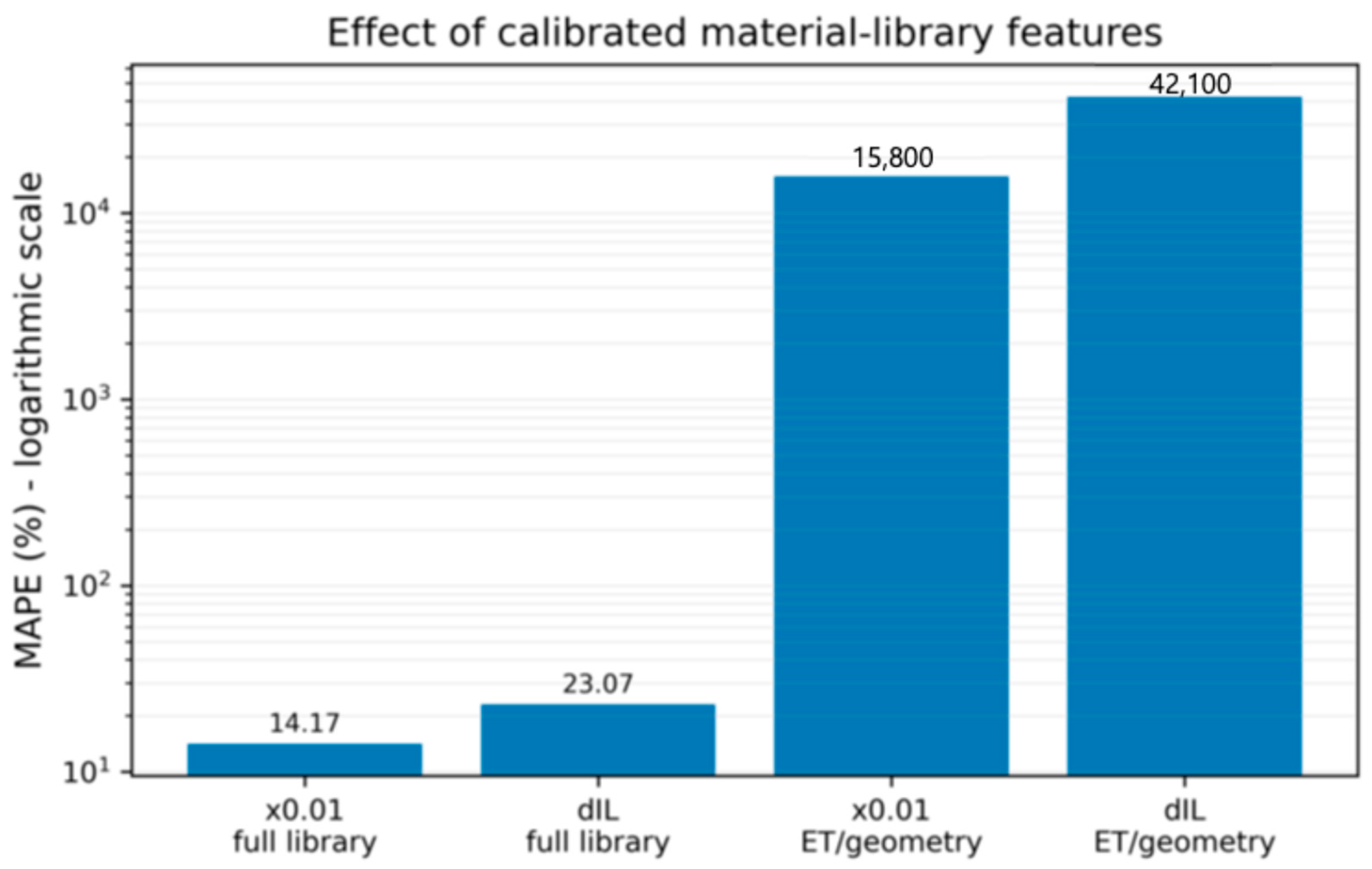
10].
Conventional analysis of buried metal diffusion and interfacial reaction relies on SIMS, TEM/EDS, XPS, or other physical and chemical analysis methods [
1,
3,
4,
5]. These methods provide direct information on concentration profiles and interfacial structure, but they are not well suited for rapid inline monitoring of every wafer. Electrical test-element-group (TEG) structures offer a complementary route because metal contamination and reaction-layer formation can be converted into measurable resistance, leakage, or capacitance changes [
11,
12,
13,
14,
15,
16,
17,
18,
19]. Related device-parameter extraction studies have also shown that machine-learning-based interpretation can reveal physically meaningful trends in semiconductor devices [
20]. However, the mapping from electrical response to buried degradation state is highly nonlinear because the measured resistance depends on the spatial distribution of the concentration profile, while the measured capacitance depends on a series combination of position-dependent dielectric constants and interfacial layers.
The present work addresses this inverse-monitoring problem using a physics-informed modeling and machine-learning framework.
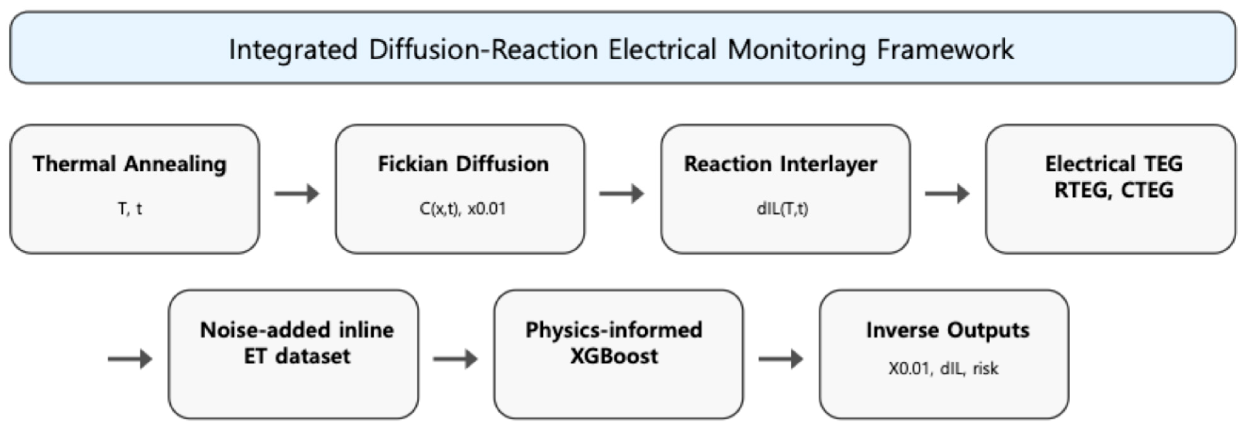
Figure 1 summarizes the concept. Thermal annealing determines the metal concentration profile and reaction-interlayer thickness. These hidden states are converted into resistance and capacitance of lateral and vertical TEGs. Finally, a physics-informed XGBoost model estimates the diffusion front, interlayer thickness, and process-risk class from noise-added electrical data.
The contributions of this work are as follows. First, a unified diffusion–reaction model is formulated for metal migration and reaction-interlayer formation in oxide dielectrics. Second, adjacent-electrode resistance and vertical capacitance TEG responses are derived using integral electrical models rather than step-profile approximations. Third, a model-generated dataset with inline measurement uncertainty is constructed and used to train XGBoost-based inverse models [
21,
22]. Finally, feature-importance analysis is used to identify which electrical and calibrated material-library parameters govern diffusion-front and interlayer-thickness extraction [
23,
24,
25,
26,
27].
2. Physics-Based Integrated Diffusion–Reaction Model
2.1. Metal Diffusion in a Semi-Infinite Oxide
The oxide is approximated as a semi-infinite medium along the positive diffusion coordinate x, where x = 0 corresponds to the metal/oxide interface. The symbol tox denotes the physical oxide thickness of the vertical capacitance TEG, whereas L
gap denotes the lateral electrode spacing of the resistance TEG. Under the first-order assumption of a constant diffusion coefficient, the metal concentration
C(
x,
t) follows Fick’s second law:
The semi-infinite approximation is used only for deriving the local concentration profile near the metal/oxide interface. In the finite electrical TEG calculations, the physically relevant penetration length is limited by the actual geometry. Therefore, when x
0.01 exceeds tox or L
gap, it is interpreted as a diffusion-length descriptor indicating saturated vertical or lateral penetration rather than as a literal oxide thickness. Under the boundary conditions
,
, and
, the complementary-error-function solution is obtained [
6,
7,
8]:
Equation (2) is the standard complementary-error-function solution of Fick’s second law for a semi-infinite medium with constant surface concentration. The temperature-dependent diffusion coefficient is described by an Arrhenius relation:
where
is the diffusion prefactor,
is the activation energy,
is the Boltzmann constant, and
is the absolute temperature. A threshold diffusion front
is defined as the position at which the normalized concentration reaches
:
In this work, x0.01 denotes the 1% diffusion-front descriptor. Because x0.01 is defined in the semi-infinite diffusion coordinate, it can exceed tox. This does not mean that the physical oxide thickness exceeds several micrometers; rather, it indicates that the vertical oxide is fully penetrated within the modeled concentration threshold. For device interpretation, the effective vertical and lateral penetrations are therefore defined as xvert,eff = min(x0.01,tox) and xlat,eff = min(x0.01,Lgap).
2.2. Reaction-Interlayer Formation
In addition to diffusion, the metal and oxide can react at the interface and form a modified interlayer. This reaction layer can represent a metal-rich oxide, an oxygen-deficient region, a mixed interfacial compound, or a process-damaged dielectric layer. The present model does not assign a unique chemical phase; instead, it treats the reaction layer as a phenomenological interfacial layer whose material constants must be calibrated for each metal/oxide stack.
The interlayer thickness
is modeled using a phenomenological parabolic growth law commonly used to describe diffusion- or reaction-limited interfacial processes [
6,
8,
14]:
Equation (6) is a phenomenological parabolic growth expression used to represent diffusion- or reaction-limited interfacial-layer formation. It is not intended to identify a unique chemical phase. The parameters kIL,0, EIL, and dsat must be calibrated for a specific metal/oxide stack using physical or electrical reference data. The reaction-rate coefficient follows an Arrhenius form:
where
and
are the reaction prefactor and activation energy with material-library parameters. The saturation thickness
prevents unphysical growth beyond the process-limited reaction region.
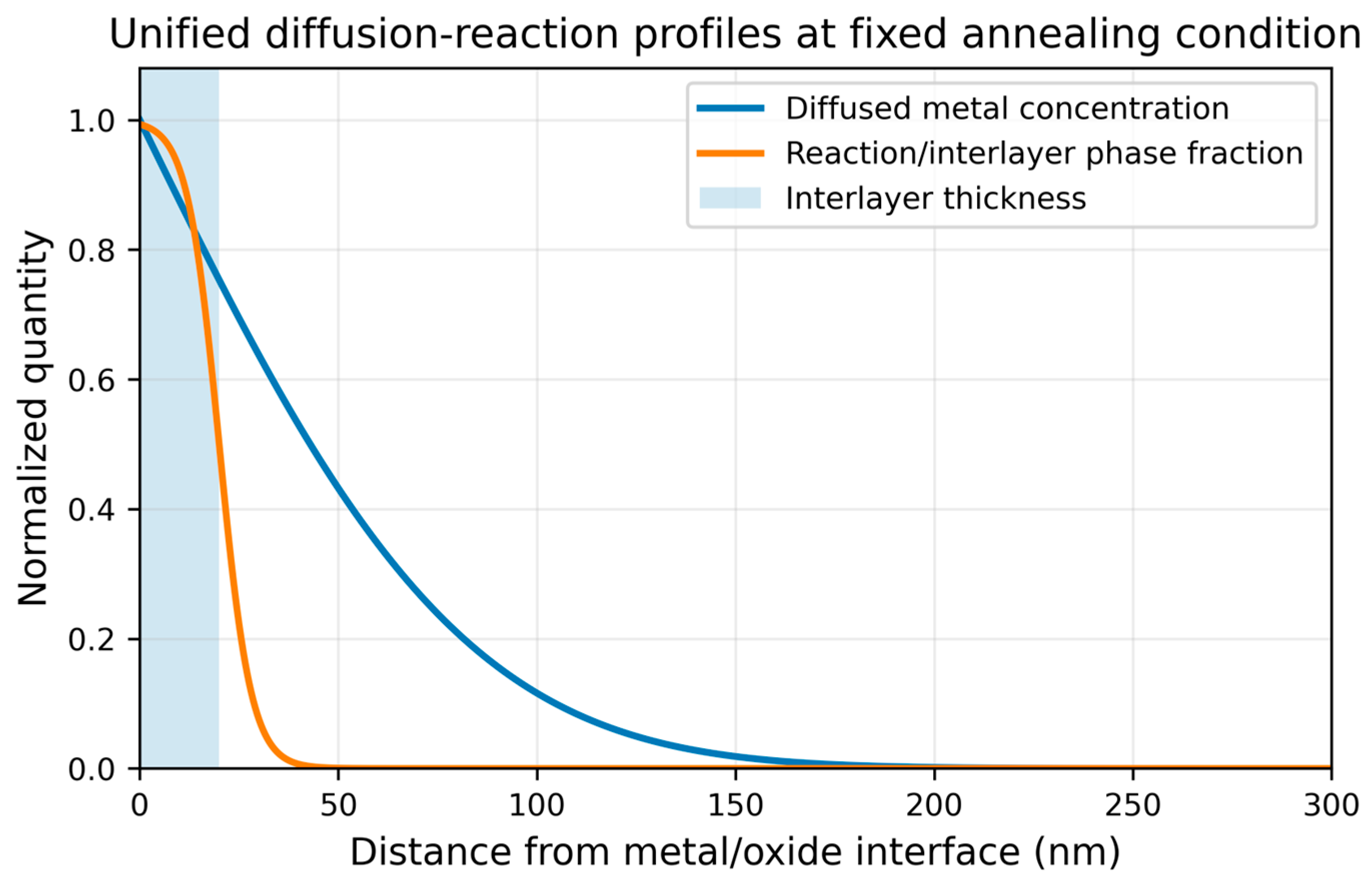
Figure 2 illustrates the unified physical state used in the simulation. The erfc-type metal concentration decays continuously into the oxide, whereas the reaction interlayer is represented as a finite region close to the interface. The orange curve in
Figure 2 indicates that the reaction-layer phase fraction is localized near the metal/oxide interface, while the blue curve represents the longer-range diffused metal concentration. The representative d
IL of approximately 20 nm is used only for visualization and is not claimed as a universal experimental value.
2.3. Concentration-Dependent Conductivity and Resistance TEG Response
The resistance and capacitance values used in this study are not direct experimental measurements. They are model-generated electrical TEG responses calculated from the hidden diffusion–reaction state. In an actual fabrication line, the same quantities would correspond to wafer-level inline isolation resistance and MIM/MOS capacitance measured from physical TEG structures. Metal diffusion increases the effective conductivity of the oxide, particularly near the interface where the metal concentration is high. The local conductivity is expressed as
The resistance values used in the database were obtained by numerical integration of the local conductivity along the lateral TEG spacing. In an experimental implementation, the corresponding value would be obtained from wafer-level adjacent-electrode leakage or isolation-resistance measurements. Where is the intrinsic oxide conductivity, is the metal-assisted conductivity prefactor, and describes the nonlinearity of concentration-assisted conduction.
The reaction interlayer can also contribute to lateral conduction near the interface. For a lateral adjacent-electrode TEG with electrode spacing
, width
, and oxide thickness
, the effective local conductivity is written as
where
is the effective interlayer conductivity,
is the Heaviside function, and
denotes the vertical distance from the interface. For the compact lateral model used here, the interlayer contribution is included through an effective conductivity enhancement factor in the TEG cross-section. The total lateral resistance is then calculated as a continuous series resistance:
Equation (11) captures the fact that diffusion does not create an abrupt step junction. Instead, the local resistance evolves gradually along the electrode gap.
2.4. Concentration- and Interlayer-Dependent Capacitance Response
The local dielectric constant is modeled as a function of the normalized metal concentration:
This phenomenological expression represents the case in which metal contamination, defects, oxygen deficiency, or leakage-assisted loss reduce the measured effective capacitance. The parameters
and
are therefore stack- and frequency-dependent fitting parameters rather than universal constants [
13,
14,
15].
The reaction interlayer contributes an additional series dielectric layer. For a vertical capacitance TEG with area
, the total capacitance is expressed as
where
is the effective dielectric constant of the reaction layer. Equation (11) shows that capacitance TEGs are especially sensitive to vertical reaction-layer formation and dielectric degradation. The capacitance values were calculated using a vertical series-capacitor formulation, where the reaction interlayer and the remaining concentration-modified oxide are connected in series. The parameter tox denotes the total oxide thickness of the capacitance TEG and is explicitly defined when first introduced. In practical measurements, CTEG would correspond to the measured capacitance from MIM- or MOS-type monitor capacitors at a specified frequency and bias condition.
3. Simulation Dataset and Inline Measurement Emulation
3.1. Parameter Space and Model-Generated Raw Data
The raw data used in this study were generated from the physics-informed diffusion, reaction-interlayer, and electrical TEG models. Each row was obtained by sampling thermal process conditions, diffusion parameters, reaction-layer parameters, TEG geometry, and electrical material parameters, followed by calculation of x
0.01, d
IL, R
TEG, C
TEG, and the process-risk class using Equations (1)–(13).
Table 1 summarizes the representative parameter ranges used to construct the model-generated simulation dataset.
For each condition, , , , , and a process-risk class were calculated. The risk classes were defined using diffusion-front and interlayer-thickness ratios relative to and . The reported prediction accuracy therefore quantifies inverse-extraction performance within the defined physics-informed simulation space. It should not be interpreted as a direct guarantee of absolute process accuracy for an arbitrary fabrication line without stack-specific calibration.
3.2. Noise-Added Inline Electrical Dataset
To emulate inline electrical-test conditions, stochastic perturbations were added to resistance, capacitance, process temperature, and annealing time. The noise model reflects high-resistance measurement fluctuation, capacitance-resolution limits, process-temperature uncertainty, and annealing-time variation. This prevents the model from learning an ideal deterministic database and allows robustness to be evaluated under measurement-like perturbations. High-resistance measurements were assigned larger relative uncertainty, while capacitance was perturbed using pF-level absolute noise and small relative uncertainty. The resulting data therefore represent noisy TEG responses rather than ideal model outputs.
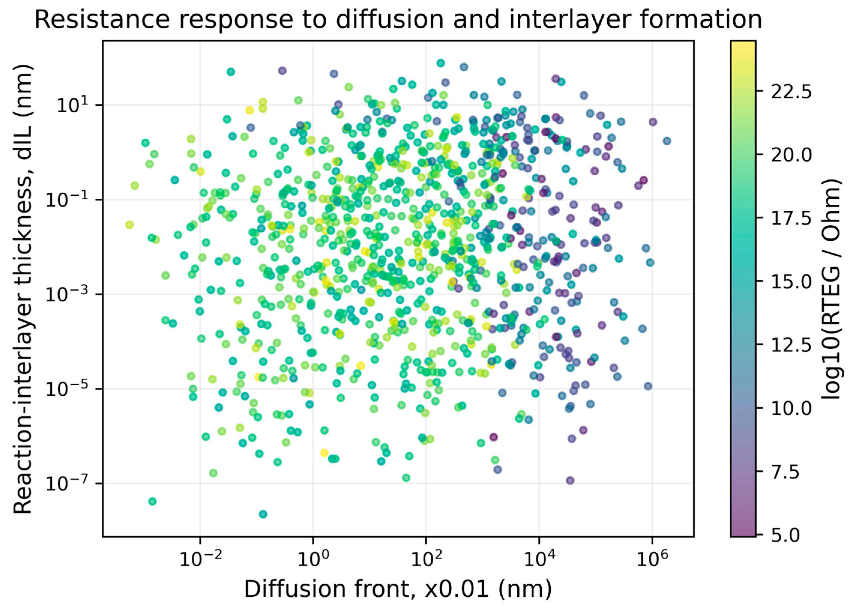
Figure 3 shows the simulated resistance response over the combined diffusion–interlayer state space. The color scale indicates
; resistance decreases as diffusion front and interlayer formation increase.
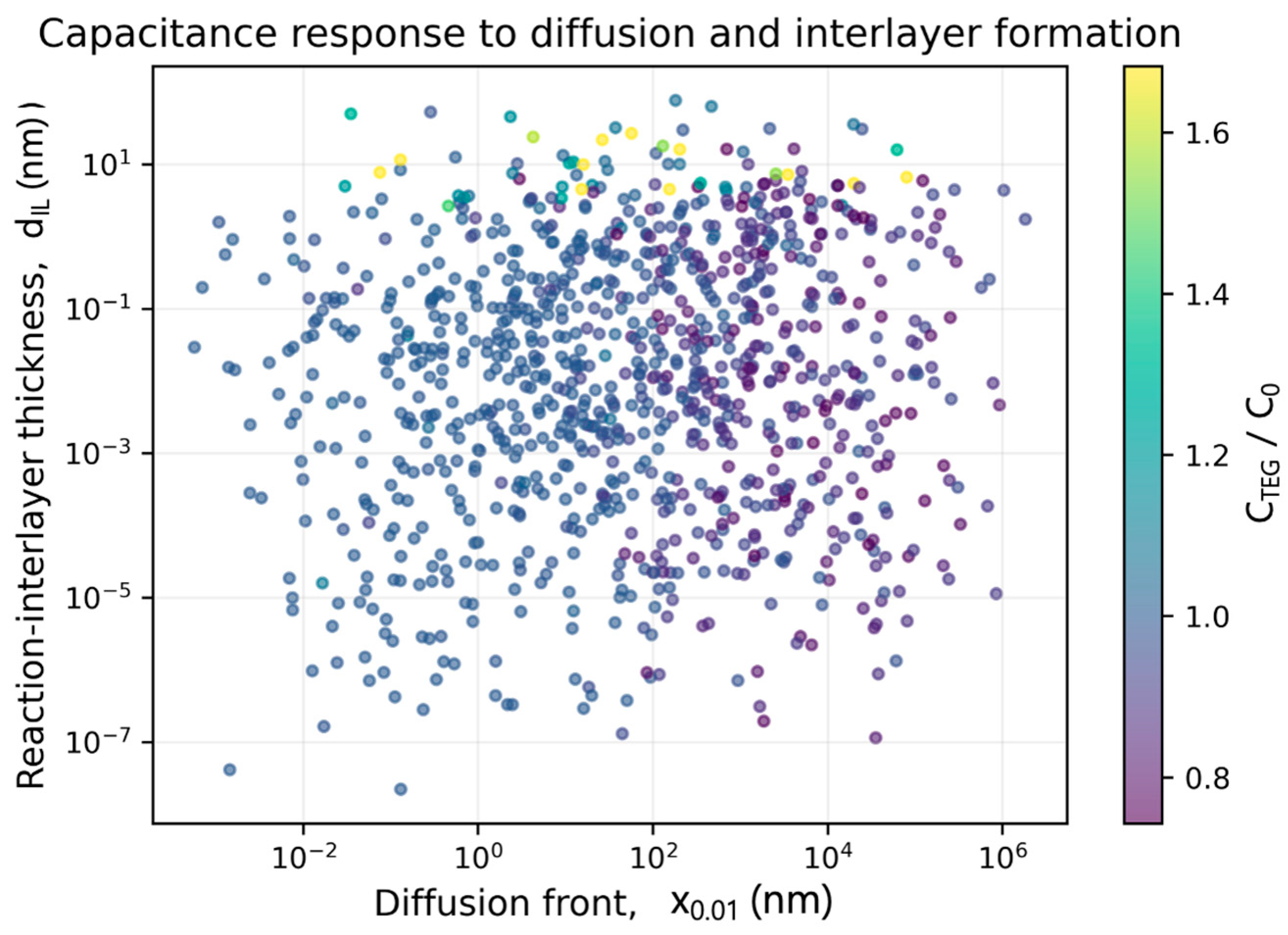
Figure 4 shows the corresponding capacitance response, where
is especially sensitive to interlayer formation and dielectric degradation. The quality of the noise-added database was evaluated by comparing noiseless and noisy electrical responses and by checking the relative deviation distributions. The distributions were centered near zero, indicating that the perturbation does not introduce systematic bias while preserving the physical trends of the ideal model.
4. XGBoost-Based Inverse Extraction
4.1. Feature Sets and Targets
The inverse problem is formulated as the estimation of hidden physical states from electrical observables and process information. Two feature sets were considered. The ET/geometry-only feature set includes , , process temperature, annealing time, , , , , and normalized capacitance-loss features. The calibrated full-library feature set additionally includes material-library parameters such as , , , , , , , and . In practical inline use, these library parameters are obtained from baseline calibration wafers and are not treated as unknown measurements. The dataset was divided into independent training and test subsets. Model performance was evaluated only on data not used for training. Additional generalization checks were defined using unseen-geometry, unseen-parameter, and noise-sensitivity splits to evaluate whether the model learned physically meaningful relationships rather than memorizing sampled cases. The primary regression targets are the 1% diffusion front and the reaction-interlayer thickness . The classification target is the process-risk class: safe, warning, or fail.
4.2. XGBoost Model and Performance Metrics
XGBoost was selected because tree-boosting models can capture nonlinear feature interactions and are robust to heterogeneous feature scales [
21,
22]. At boosting step
, the prediction is updated as
where
is the learning rate and
is the regression tree added at step
. Regression performance was quantified using RMSE,
, and MAPE:
RMSE represents the root mean square error, R
2 quantifies the coefficient of determination, and MAPE evaluates the average relative prediction error. These metrics were used for diffusion-front and interlayer-thickness regression, while the risk classifier was evaluated using accuracy and the confusion matrix. The inverse extraction problem can also be written as a weighted least-squares objective:
where
may include
,
, or a process-damage index. Equation (15) provides the analytical inverse-extraction baseline, whereas XGBoost learns a more flexible nonlinear mapping from a high-dimensional feature set.
5. Results and Discussion
5.1. Inverse Extraction of Diffusion Front
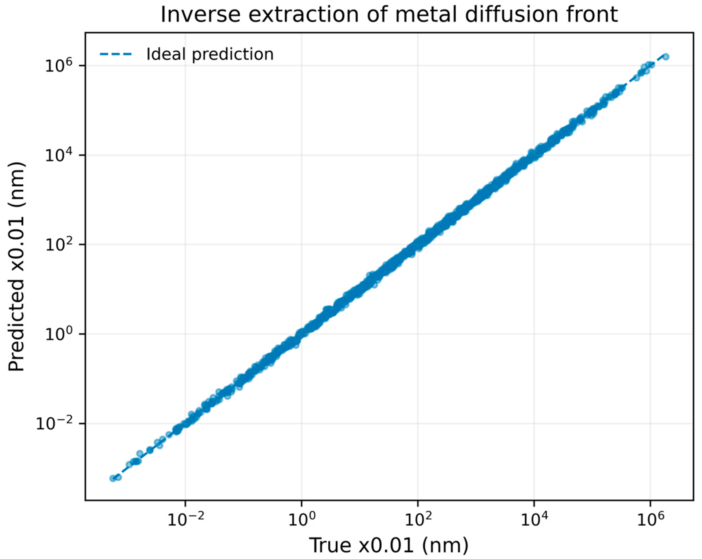
Figure 5 compares the true and predicted diffusion fronts using the calibrated full-library feature set. The predicted values closely follow the ideal line over several orders of magnitude.
Table 2 shows that the full-library XGBoost model achieves an RMSE of 23,935 nm, an
of 0.959, and a MAPE of 14.17% for
. The relatively broad RMSE reflects the logarithmically wide target range, whereas the high
and moderate MAPE indicate that the model captures the dominant diffusion physics across the sampled material-library space. Because x
0.01 is defined along the semi-infinite diffusion coordinate, large values of x
0.01 can exceed the oxide thickness tox. Such cases are interpreted as full penetration of the vertical oxide region, and the effective vertical penetration is limited as x
vert,eff = min(x
0.01, tox). For lateral TEG interpretation, the effective lateral penetration is similarly limited as x
lat,eff = min(x
0.01, L
gap). Thus, x
0.01 should be interpreted as a diffusion-length descriptor, while device-level penetration is limited by the finite TEG geometry.
5.2. Inverse Extraction of Reaction-Interlayer Thickness
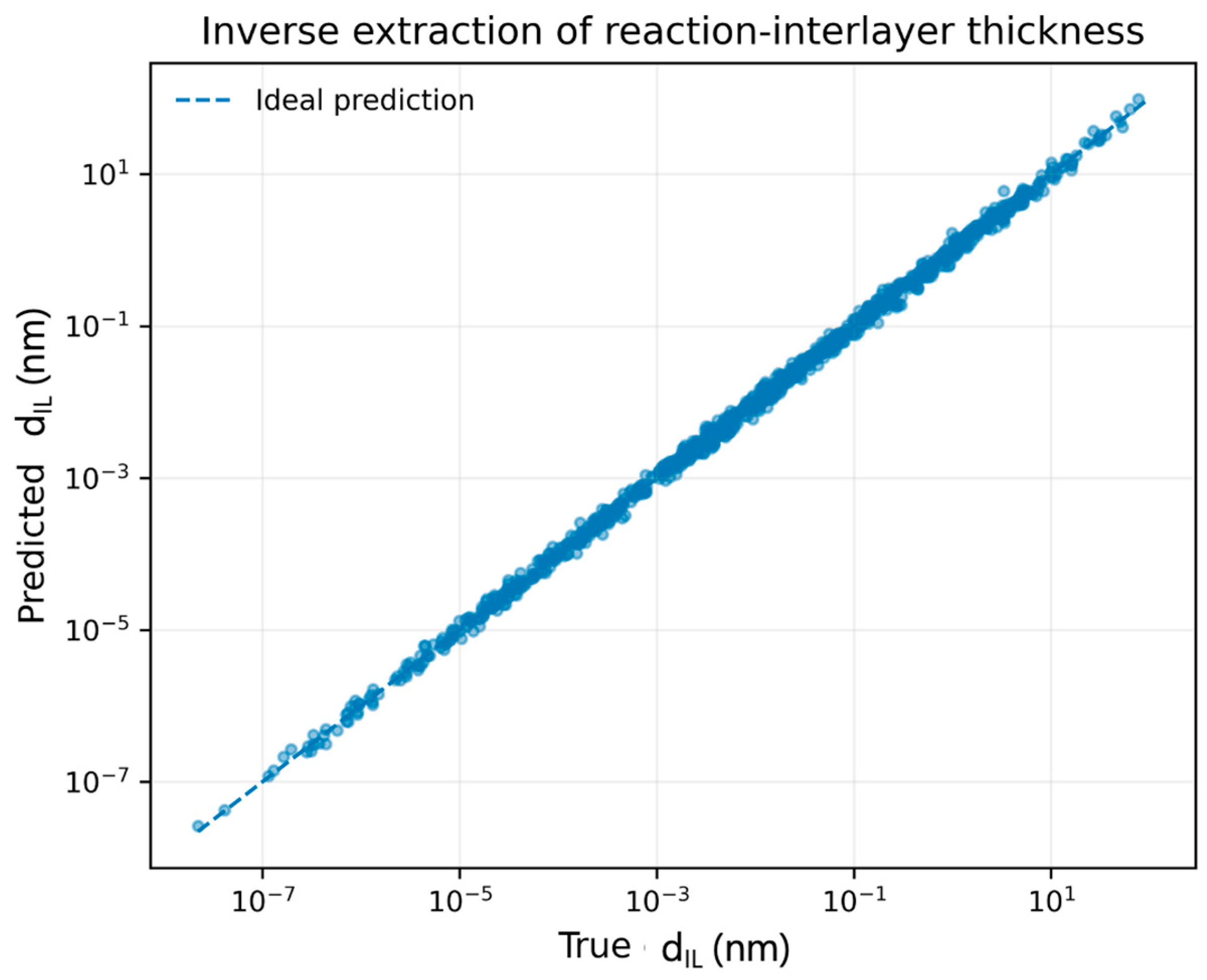
Figure 6 shows the predicted reaction-interlayer thickness. The interlayer extraction task is more difficult than diffusion-front extraction because capacitance response can partially saturate and because different combinations of
,
, and dielectric-degradation parameters can produce similar capacitance shifts. Nevertheless, the full-library model achieves an
of 0.802 and a MAPE of 23.07%, demonstrating that a calibrated material library enables quantitative estimation of
.
5.3. Resistance and Capacitance Provide Complementary Information
The feature-importance results in
Figure 7 and
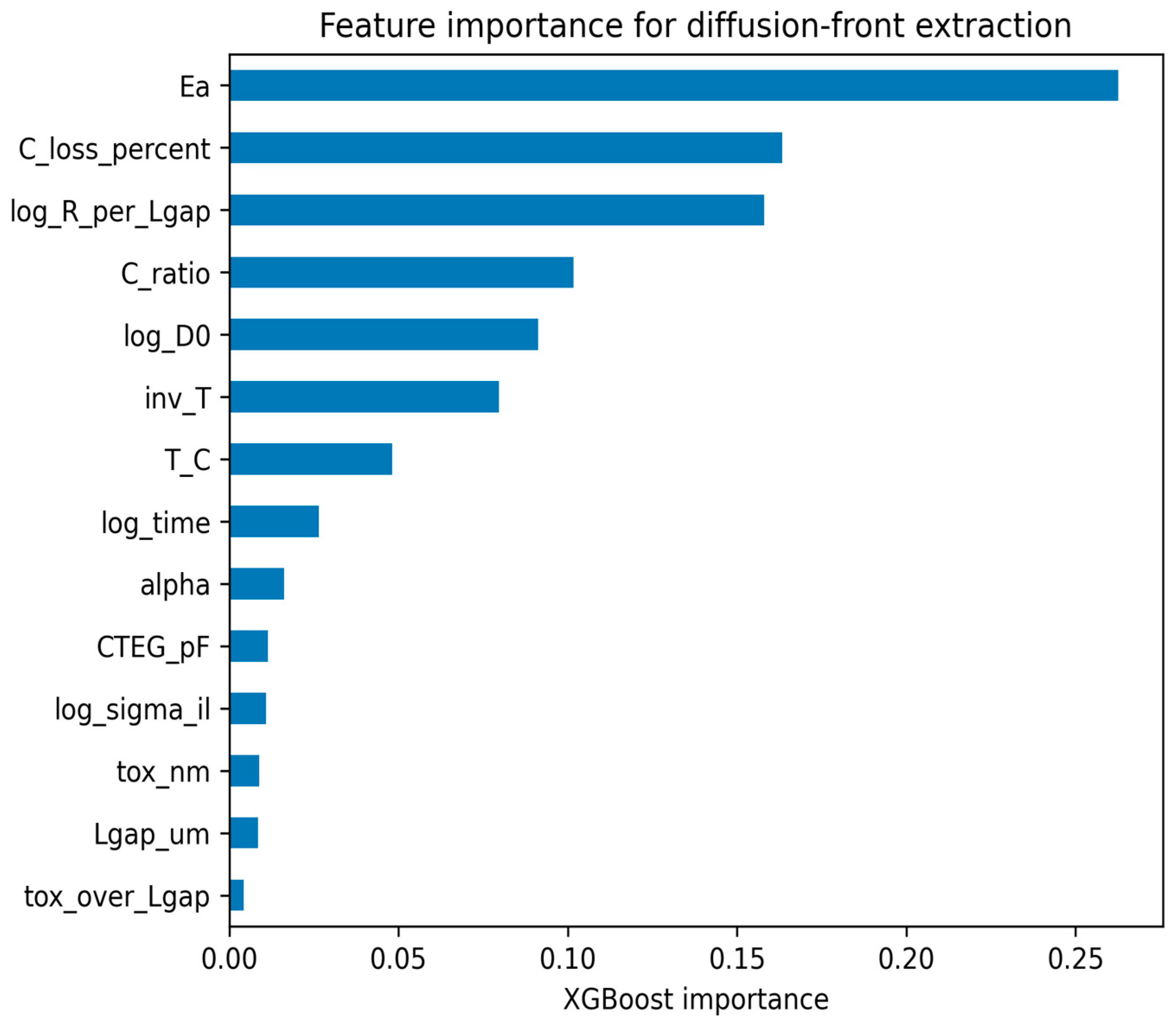
Figure 8 show that the two inverse tasks rely on different physical observables. For diffusion-front extraction, activation energy, capacitance-loss percentage, normalized resistance-per-gap, capacitance ratio, diffusion prefactor, and inverse temperature are dominant features (
Figure 7). This is physically reasonable because
is governed by
and by the lateral formation of metal-assisted conductive paths. Feature importance values in
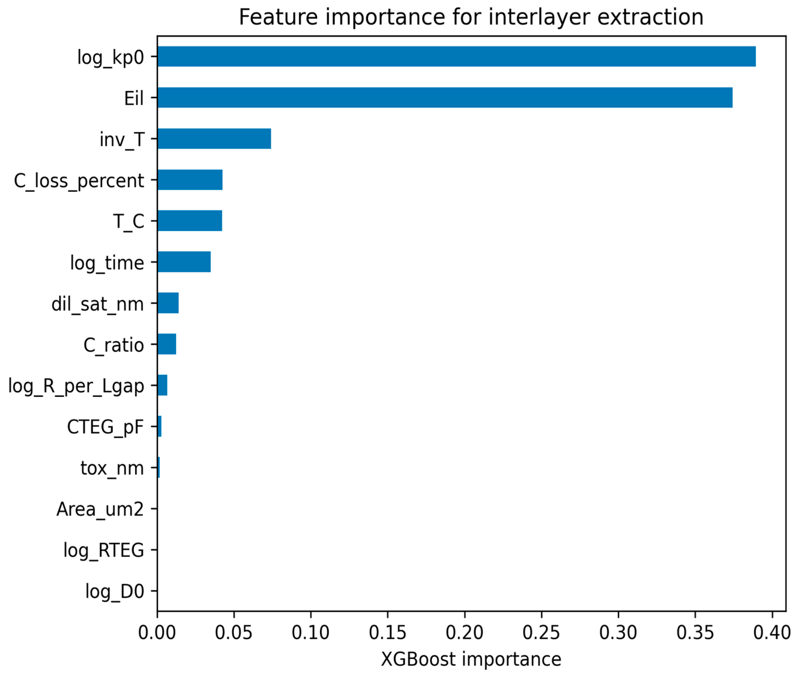
Figure 7 and
Figure 8 were calculated using the normalized gain metric from the trained XGBoost trees. The gain metric quantifies the average reduction in the loss function obtained when a feature is used for tree splitting, and the values were normalized so that the total importance equals one.
For interlayer-thickness extraction, the reaction prefactor
and reaction activation energy
dominate, followed by inverse temperature and capacitance-loss features (
Figure 8). This confirms that
is mainly governed by reaction kinetics and capacitance response. Therefore,
and
should be interpreted as complementary indicators rather than redundant measurements.
5.4. Effect of Calibrated Material Library
Figure 9 summarizes the inverse-extraction performance for the ET/geometry-only and full-library feature sets. The ET/geometry-only feature set can classify risk states with reasonable accuracy, but quantitative extraction of
and
is limited because many different material parameter combinations can produce similar electrical responses. The full-library feature set resolves this ambiguity by supplying calibrated stack-specific physical parameters. This result is important for practical deployment: inline electrical measurements are sufficient for risk monitoring after calibration, but accurate quantitative extraction requires a material library obtained from baseline physical analysis and reference TEG measurements.
5.5. Risk Classification
The proposed framework can also be used as a process-risk classifier.
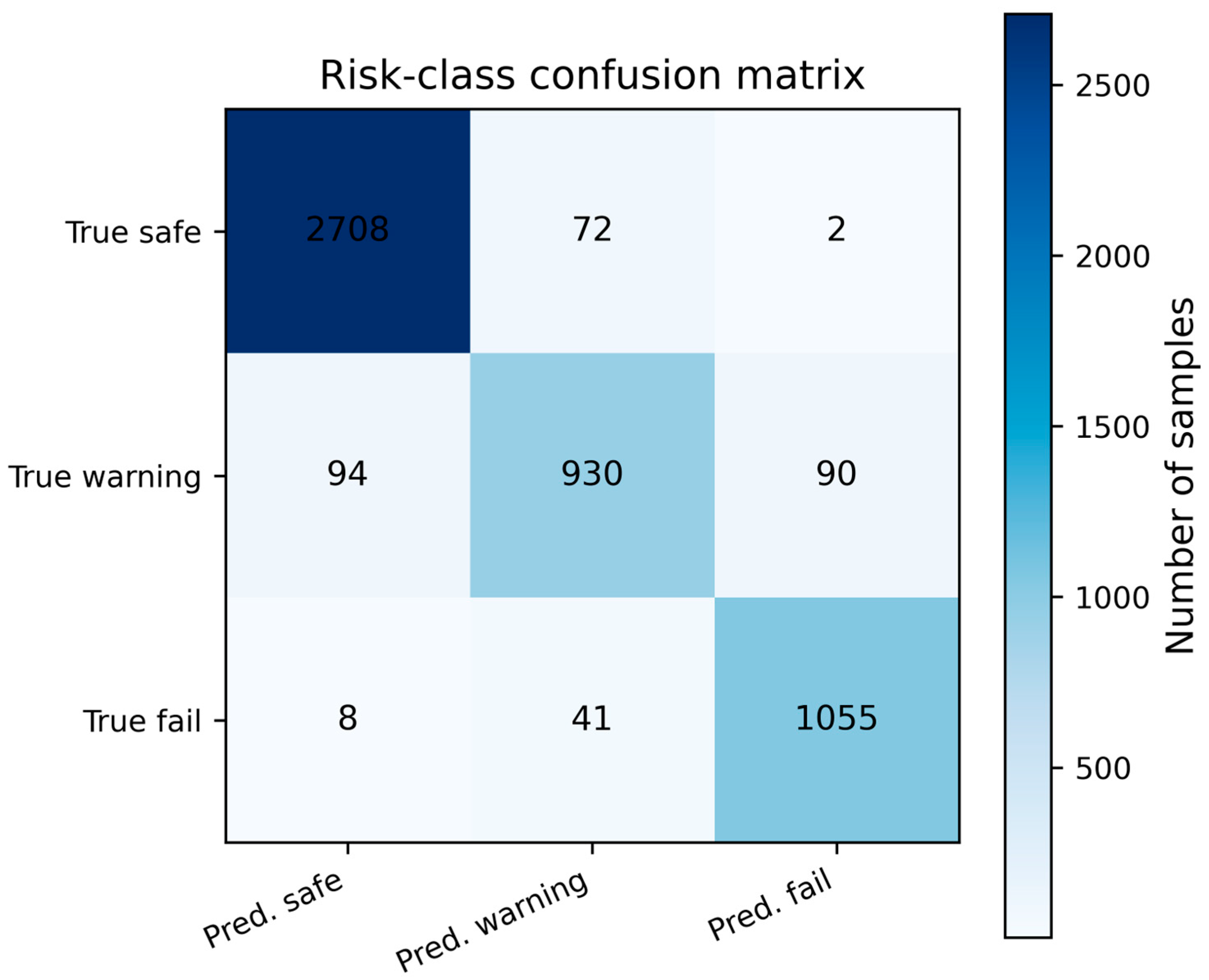
Figure 10 shows the confusion matrix for safe, warning, and fail states using the calibrated full-library classifier. The overall accuracy is 93.86%. Most errors occur between adjacent safe/warning or warning/fail classes, which is expected because these boundaries correspond to continuous degradation metrics rather than abrupt physical transitions. The numerical values of the confusion matrix are listed in
Table 3.
5.6. Generalization and Sensitivity Analysis
To evaluate the generalization capability of the proposed framework, three validation scenarios were considered: random split, unseen-geometry split, and unseen-material-parameter split. The random split evaluates interpolation within the sampled process space, whereas the unseen-geometry and unseen-parameter tests evaluate transferability to layouts or material-library conditions not directly included in the training subset.
A perturbation-based sensitivity analysis was performed by varying major diffusion, reaction, geometry, conductivity, and dielectric parameters. This analysis was used to identify which assumptions most strongly influence RTEG, CTEG, x0.01, and dIL.
6. Implications for Inline Process Monitoring
The results support a practical monitoring strategy. First, calibration wafers are characterized using SIMS, TEM/EDS, XPS, C–V, and I–V measurements to establish the material-library parameters for a target metal/oxide stack. Second, resistance and capacitance TEGs are distributed across product or monitor wafers. Third, inline ET measurements are mapped to diffusion-front, interlayer-thickness, and risk-class outputs using the trained inverse model. Finally, when the extracted risk index exceeds the control limit, the annealing condition, barrier process, interface cleaning, or metal-stack design can be adjusted.
The proposed model should not be interpreted as a replacement for physical analysis. Instead, it provides a fast electrical screening and monitoring tool that can reduce the number of wafers requiring destructive or time-intensive physical characterization. The framework is particularly useful when diffusion and interfacial reactions occur simultaneously and cannot be separated using a single electrical observable. Transferability is therefore hierarchical. Within the same calibrated stack, the model can be transferred across TEG layouts by including geometry features such as Lgap, tox, W, and A. Across different metal/oxide stacks, diffusion and reaction parameters must be recalibrated before quantitative extraction is claimed.
7. Limitations
The present study is based on physics-informed model-generated datasets. Therefore, the reported numerical extraction accuracy should be interpreted as a simulation-based demonstration of feasibility, not as a calibrated value for a specific metal/oxide process. The reaction interlayer is modeled phenomenologically, and its effective conductivity and dielectric constant may depend on phase composition, oxygen deficiency, frequency, measurement voltage, and thermal history. Future work should calibrate the model using stack-specific SIMS, TEM/EDS, XPS, frequency-dependent C–V, leakage I–V, and long-term stress TEG data. In addition, finite-element simulations can be used to relax the one-dimensional semi-infinite approximation and account for corner effects, nonuniform fields, and realistic electrode geometry. To avoid overclaiming, the present accuracy values represent simulation-based inverse-extraction accuracy. Material-specific process accuracy must be established using experimental calibration data from SIMS, TEM/EDS, STEM/EELS, XPS, C-V, I-V, or long-term reliability TEG measurements.
8. Conclusions
This study proposed an integrated electrical TEG modeling framework for monitoring metal diffusion and reaction-interlayer formation in oxide dielectrics during thermal annealing. Metal diffusion was described by a Fick–Arrhenius erfc profile, while reaction-interlayer growth was represented using a parabolic Arrhenius reaction model. These hidden physical states were coupled to adjacent-electrode resistance and vertical capacitance TEG responses through integral electrical models. A physics-informed dataset with inline measurement uncertainty was then used to train XGBoost models for inverse extraction.
The calibrated full-library model achieved an of 0.959 for 1% diffusion-front extraction, an of 0.802 for reaction-interlayer-thickness extraction, and a risk-classification accuracy of 93.86%. Resistance TEGs were primarily sensitive to lateral metal-assisted conduction, while capacitance TEGs provided complementary sensitivity to vertical interlayer formation and dielectric degradation. These results indicate that combined resistance and capacitance TEG measurements can be used to electrically monitor multiple manufacturing risks, including metal diffusion, barrier degradation, and metal/oxide reaction. After stack-specific calibration, the proposed framework can support non-destructive inline estimation of diffusion extent, interlayer formation, and process-risk state.
Author Contributions
Conceptualization, S.K.H.; methodology, H.A.Y., J.Y.L. and S.K.H.; software, H.A.Y. and J.Y.L.; validation, H.A.Y., J.Y.L. and S.K.H.; formal analysis, H.A.Y. and J.Y.L.; investigation, H.A.Y. and J.Y.L.; writing—original draft preparation, H.A.Y., J.Y.L. and S.K.H.; writing—review and editing, S.K.H.; supervision, S.K.H.; project administration, S.K.H.; funding acquisition, S.K.H. All authors have read and agreed to the published version of the manuscript.
Funding
This work was supported by the Seoul National University of Science and Technology.
Data Availability Statement
The data presented in this study are available on request from the corresponding author due to institutional data-management limitations and the large volume of simulation files. The raw data supporting the conclusions of this article will be made available by the authors on request.
Conflicts of Interest
The authors declare no conflicts of interest.
References
- McBrayer, J.D.; Swanson, R.M.; Sigmon, T.W. Diffusion of metals in silicon dioxide. J. Electrochem. Soc. 1986, 133, 1242–1246. [Google Scholar] [CrossRef]
- Wang, S.Q. Barriers against copper diffusion into silicon and drift through silicon dioxide. MRS Bull. 1994, 19, 30–40. [Google Scholar] [CrossRef]
- Fisher, I.; Eizenberg, M. Copper ion diffusion in porous and nonporous SiO2-based dielectrics using bias thermal stress and thermal stress tests. Thin Solid Films 2008, 516, 4111–4121. [Google Scholar] [CrossRef]
- Byrne, C.; Brennan, B.; Lundy, R.; Bogan, J.; Gomeniuk, Y.Y.; Monaghan, S.; Hurley, P.K.; Hughes, G. Physical, chemical and electrical characterisation of the diffusion of copper in silicon dioxide and prevention via a CuAl alloy barrier layer system. Mater. Sci. Semicond. Process. 2017, 63, 227–236. [Google Scholar] [CrossRef]
- Mondon, F.; Cluzel, J.; Blachier, D.; Morand, Y.; Martel, L.; Reimbold, G. Electrical characterization of copper penetration effects in the gate oxide of MOS devices. MRS Online Proc. Libr. 2001, 714, 8121. [Google Scholar] [CrossRef]
- Crank, J. The Mathematics of Diffusion, 2nd ed.; Oxford University Press: Oxford, UK, 1975. [Google Scholar]
- Shewmon, P.G. Diffusion in Solids, 2nd ed.; TMS: Warrendale, PA, USA, 1989. [Google Scholar]
- Mehrer, H. Diffusion in Solids: Fundamentals, Methods, Materials, Diffusion-Controlled Processes; Springer: Berlin/Heidelberg, Germany, 2007. [Google Scholar]
- Nawaz, M.Z.; Ahmad, W.; Hasan, I.M.u.; Gulzar, H.; Hasan, W.u.; Younis, U.; Farooq, A.; Saleem, M.S.; Li, M.; Chu, P.K. Modern 2D heterostructures: From fabrication challenges to emerging applications. Small Methods 2026, 10, e02365. [Google Scholar] [CrossRef] [PubMed]
- Nawaz, M.Z.; Jiang, X.; Qin, T.; Khalid, M.; Xi, W.; Hasan, W.u.; Hasan, I.M.u.; Li, M.; Zeng, Y.; Yang, X. 2D Bi2O2Se: Structure-property evolution, electronic tunability and technological prospects. Coord. Chem. Rev. 2026, 564, 218074. [Google Scholar] [CrossRef]
- Schroder, D.K. Semiconductor Material and Device Characterization, 3rd ed.; Wiley: Hoboken, NJ, USA, 2006. [Google Scholar]
- Sze, S.M.; Ng, K.K. Physics of Semiconductor Devices, 3rd ed.; Wiley: Hoboken, NJ, USA, 2007. [Google Scholar]
- Jonscher, A.K. Dielectric relaxation in solids. J. Phys. D Appl. Phys. 1999, 32, R57–R70. [Google Scholar] [CrossRef]
- McPherson, J.W. Reliability Physics and Engineering: Time-to-Failure Modeling, 3rd ed.; Springer: Cham, Switzerland, 2019. [Google Scholar]
- Chen, T.; Guestrin, C. XGBoost: A scalable tree boosting system. In Proceedings of the 22nd ACM SIGKDD International Conference on Knowledge Discovery and Data Mining, San Francisco, CA, USA, 13–17 August 2016; pp. 785–794. [Google Scholar]
- Lundberg, S.M.; Lee, S.-I. A unified approach to interpreting model predictions. Adv. Neural Inf. Process. Syst. 2017, 30, 4765–4774. [Google Scholar]
- Breiman, L. Random forests. Mach. Learn. 2001, 45, 5–32. [Google Scholar] [CrossRef]
- Friedman, J.H. Greedy function approximation: A gradient boosting machine. Ann. Stat. 2001, 29, 1189–1232. [Google Scholar] [CrossRef]
- Hastie, T.; Tibshirani, R.; Friedman, J. The Elements of Statistical Learning: Data Mining, Inference, and Prediction, 2nd ed.; Springer: New York, NY, USA, 2009. [Google Scholar]
- Edelstein, D.C.; Heidenreich, J.; Goldblatt, R.; Cote, W.; Uzoh, C.; Lustig, N.; Roper, P.; McDevitt, T.; Motsiff, W.; Simon, A.; et al. Full copper wiring in a sub-0.25 μm CMOS ULSI technology. In Proceedings of the IEEE International Electron Devices Meeting, Washington, DC, USA, 7–10 December 1997; pp. 773–776. [Google Scholar]
- Rosenberg, R.; Edelstein, D.C.; Hu, C.-K.; Rodbell, K.P. Copper metallization for high performance silicon technology. Annu. Rev. Mater. Sci. 2000, 30, 229–262. [Google Scholar] [CrossRef]
- Murarka, S.P.; Hymes, S.W. Copper metallization for ULSI and beyond. Crit. Rev. Solid State Mater. Sci. 1995, 20, 87–124. [Google Scholar] [CrossRef]
- Scott, D.B.; Hunter, W.R.; Shichijo, H. A transmission line model for silicided diffusions: Impact on the performance of VLSI circuits. IEEE Trans. Electron Devices 1982, 29, 651–661. [Google Scholar] [CrossRef]
- Baraskar, A.; Gossard, A.C.; Rodwell, M.J.W. Lower limits to metal–semiconductor contact resistance: Theoretical models and experimental data. J. Appl. Phys. 2013, 114, 154516. [Google Scholar] [CrossRef]
- Hong, T.; Hong, S. Performance impact analysis of resistance elements in field-effect transistors utilizing 2D channel materials. J. Microelectron. Packag. Soc. 2023, 30, 83–87. [Google Scholar]
- Oh, S.; Hong, S. Analysis of the impact of alignment errors on electrical signal transmission efficiency in interconnect and bonding structures. J. Microelectron. Packag. Soc. 2024, 31, 38–41. [Google Scholar]
- Lee, S.W.; Ban, H.J.; Park, J.K.; Ji, D.J.; Hong, S.K. Analyzing the influence of source/drain growth height and lateral growth depth in FinFETs through XGBoost and SHAP. IEEE Electron Device Lett. 2024, 45, 1714–1716. [Google Scholar] [CrossRef]
Figure 1.
Workflow of the proposed integrated diffusion–reaction electrical monitoring framework. Thermal annealing determines the metal concentration profile and reaction-interlayer thickness; the resulting electrical TEG responses are used for inverse extraction through a physics-informed XGBoost model.
Figure 1.
Workflow of the proposed integrated diffusion–reaction electrical monitoring framework. Thermal annealing determines the metal concentration profile and reaction-interlayer thickness; the resulting electrical TEG responses are used for inverse extraction through a physics-informed XGBoost model.
Figure 2.
Representative unified diffusion–reaction profile at a fixed annealing condition (T = 400 C and t = 60 min). The blue curve shows the erfc-type diffusion concentration profile, and the orange curve shows the smoothed spatial interlayer phase fraction fIL(x,T,t). The shaded region indicates an illustrative interlayer thickness of approximately 20 nm.
Figure 2.
Representative unified diffusion–reaction profile at a fixed annealing condition (T = 400 C and t = 60 min). The blue curve shows the erfc-type diffusion concentration profile, and the orange curve shows the smoothed spatial interlayer phase fraction fIL(x,T,t). The shaded region indicates an illustrative interlayer thickness of approximately 20 nm.
Figure 3.
Simulated adjacent-electrode resistance response over the integrated diffusion–interlayer state space. The color scale represents log10( by over the full data range to avoid artificial clipping or apparent discontinuity.
Figure 3.
Simulated adjacent-electrode resistance response over the integrated diffusion–interlayer state space. The color scale represents log10( by over the full data range to avoid artificial clipping or apparent discontinuity.
Figure 4.
Simulated capacitance over the integrated diffusion-interlayer state space. The color scale represents CTEG/C0 over the full displayed range, showing the influence of dielectric degradation and series reaction-layer formation.
Figure 4.
Simulated capacitance over the integrated diffusion-interlayer state space. The color scale represents CTEG/C0 over the full displayed range, showing the influence of dielectric degradation and series reaction-layer formation.
Figure 5.
True versus predicted 1% diffusion front obtained using the calibrated full-library XGBoost model.
Figure 5.
True versus predicted 1% diffusion front obtained using the calibrated full-library XGBoost model.
Figure 6.
True versus predicted reaction-interlayer thickness obtained using the calibrated full-library XGBoost model.
Figure 6.
True versus predicted reaction-interlayer thickness obtained using the calibrated full-library XGBoost model.
Figure 7.
XGBoost feature importance for diffusion-front extraction using the calibrated full-library feature set.
Figure 7.
XGBoost feature importance for diffusion-front extraction using the calibrated full-library feature set.
Figure 8.
XGBoost normalized gain-based feature importance for reaction-interlayer-thickness extraction using the calibrated full-library feature set.
Figure 8.
XGBoost normalized gain-based feature importance for reaction-interlayer-thickness extraction using the calibrated full-library feature set.
Figure 9.
Performance comparison between ET/geometry-only features and calibrated full-library features. A logarithmic MAPE scale is used because the ET/geometry-only regression errors are much larger than those of the calibrated full-library model.
Figure 9.
Performance comparison between ET/geometry-only features and calibrated full-library features. A logarithmic MAPE scale is used because the ET/geometry-only regression errors are much larger than those of the calibrated full-library model.
Figure 10.
Confusion matrix for process-risk classification using the calibrated full-library XGBoost classifier.
Figure 10.
Confusion matrix for process-risk classification using the calibrated full-library XGBoost classifier.
Table 1.
Representative parameter ranges used for model-generated dataset construction.
Table 1.
Representative parameter ranges used for model-generated dataset construction.
| Category | Parameter | Representative Range |
|---|
| Thermal process | T | 250–500 °C |
| Thermal process | t | 1–300 min |
| Diffusion | | 10−10–10−6 m2/s |
| Diffusion | | 0.5–1.8 eV |
| Reaction interlayer | | 10−18–10−10 m2/s |
| Reaction interlayer | | 0.3–1.6 eV |
| Reaction interlayer | | 1–50 nm |
| Geometry | | 0.2–10 μm |
| Geometry | | 5–500 nm |
| Geometry | | 1–100 μm |
| Capacitance geometry | | 10−10–10−6 m2 |
| Conductivity model | , , | logarithmic sampling |
| Dielectric model | , , , | stack-dependent sampling |
Table 2.
XGBoost inverse-extraction performance using the calibrated full-library feature set.
Table 2.
XGBoost inverse-extraction performance using the calibrated full-library feature set.
| Target | Model | RMSE | | MAPE or Accuracy |
|---|
| Diffusion front | Log-target XGBoost | 23,935 nm | 0.959 | 14.17% |
| Interlayer thickness | Log-target XGBoost | 2.30 nm | 0.802 | 23.07% |
| Process-risk class | XGBoost classifier | – | – | 93.86% |
Table 3.
Confusion matrix for process-risk classification.
Table 3.
Confusion matrix for process-risk classification.
| True Class | Predicted Safe | Predicted Warning | Predicted Fail |
|---|
| Safe | 2708 | 72 | 2 |
| Warning | 94 | 930 | 90 |
| Fail | 8 | 41 | 1055 |
| Disclaimer/Publisher’s Note: The statements, opinions and data contained in all publications are solely those of the individual author(s) and contributor(s) and not of MDPI and/or the editor(s). MDPI and/or the editor(s) disclaim responsibility for any injury to people or property resulting from any ideas, methods, instructions or products referred to in the content. |