1. Introduction
Modular multilevel converters (MMCs) are an interesting topology, due to their flexibility and applicability across many applications [
1,
2]. They have been used in high-voltage systems to reduce output signal distortion, distribute voltage across multiple semiconductors, enable the use of lower-voltage components, and provide redundancy options. The topology has also gained interest in mid-voltage applications and electric vehicles [
3,
4] due to its advantages. By including the batteries in the MMC modules, additional control over the batteries is achieved through their separation into smaller units. This allows precise energy consumption control, resulting in state of charge (SOC) balancing. As battery technologies continue to improve, the range of electric vehicles (EVs) is increasing and becoming available in a wider range of applications. Besides electric cars, efforts have been made to electrify lighter and heavier delivery vehicles. Such vehicles, as well as personal cars, rely on power converter fault tolerance to operate under any conditions within the manufacturer’s specifications and complete the journey. If an internal converter fault occurs during operation, the vehicle will not reach the desired destination unless the power converter has fault-tolerant capabilities.
A potential topology that can provide different levels of redundancy without major structural changes is the MMC. Redundant operation can be achieved at different levels by using software or hardware modifications. Software modifications require no hardware changes, and, in the majority of cases, result in degraded operation [
5]. This allows electric vehicles to continue their journey to the desired destination with reduced power. If a hardware modification is used, a redundant module can be added to the topology to replace the faulted one [
6]. This allows unchanged performance after a fault, at the cost of increased converter volume and additional components. Similar redundancy operations can be achieved by integrating the battery in the MMC topology. By using the software redundancy method, a module will be excluded from operation after a fault occurs. This results in partial battery capacity loss, degrading the vehicle’s range. If an additional module is added to the topology, its battery increases the overall capacity of the topology. When a fault occurs, a module will again be excluded from operation, reducing the battery’s capacity to its original state and degrading the vehicle’s range further. Despite these disadvantages, researchers focus mainly on using software modifications to mitigate fault occurrence in a module and continue operating with degraded performance [
7].
When using MMCs with integrated batteries [
8], a sorting algorithm is required to maintain similar module voltage levels and SOC [
9,
10]. This is important for the symmetrical operation of the converter. If one module’s battery voltage deviates from the others, a voltage step of a different amplitude will appear at the converter output, resulting in a degraded output current waveform. This causes additional losses in the load and should be avoided. Sorting algorithms are generally capable of post-fault operation with the faulted module excluded from the operation. In the case of modules with integrated batteries, this results in partial loss of the system’s battery capacity. An improved sorting algorithm was presented in [
11], designed to operate under fault conditions without excluding the faulted module while preserving access to its battery capacity. This resulted in almost uncompromised post-fault operation in the case of a single transistor fault in one module per output phase, which is ideal for EV applications. However, a drawback was observed during the continuous high output power operation, resulting in an asymmetrical output current due to the inability of the faulted module to discharge its battery sufficiently. This problem was avoided by limiting the continuous high output power.
An additional balancing system is required to eliminate the improved sorting algorithm’s drawback. The existing methods with potential compatibility include additional hardware for the module battery balancing [
12]. Passive and active examples are presented, where the passive method uses resistors to drain the excess battery energy for balancing. The active method uses an inductive balancing circuit to redistribute energy between the batteries in the converter. The passive method would be suitable in this use case, but the excess energy is wasted as heat. The active method solves the efficiency problem, but it requires additional hardware, which adds to the system complexity and cost. Another method for battery balancing uses the vehicle’s electric motor to redistribute energy between the modules [
13]. This method requires the vehicle to be stationary, which is not suitable for use in combination with the improved sorting algorithm, as the algorithm can balance the batteries sufficiently in low-power scenarios. The problem occurs during constant high output power periods, which require the vehicle to be driving. Several authors have also proposed various methods for balancing battery energy during operation [
14,
15,
16,
17]. The proposed methods include SOC balancing between three-phase legs, between the upper and lower arms of each phase, and between modules. This is achieved by varying the module output power, but it is assumed that all the modules are identical, which, in post-fault operation, they are not, as the faulted module can operate only as a half bridge. In the use case of MMC-based battery energy storage systems, the general solutions include a balancing algorithm which excludes the faulted modules from operation. In a system with a large number of modules, an excluded module does not change the system capabilities significantly, and the system can continue operating in degraded mode. In this case, the post-fault operation unbalanced module voltage levels do not occur.
The analyzed methods are designed for normal operation, and they are not intended for post-fault conditions. The modules are assumed to be identical. However, during redundant operation, the faulted modules operate in half-bridge mode. In addition, existing methods assume symmetrical compensation. In contrast, when using the improved sorting algorithm, asymmetrical compensation is required, as only one half-period is distorted.
In this work, an additional method is proposed as an extension to the improved sorting algorithm, which eliminates the need for a high constant power limit when the faulted module battery voltage differs significantly. A voltage compensation algorithm is introduced to achieve this. It takes into account the measured module voltage levels, and adjusts the module operating times accordingly to obtain an ideal sinusoidal output current. This process is performed separately for the positive and negative half-periods of the output signal, as different modules are used in each case. After compensating the module operating times, the reference signal amplitude is also adjusted to produce a symmetrical output sine wave. The proposed method is activated when the converter enters redundant operation.
For the validation of the proposed method, an MMC with integrated batteries was chosen, using modules with a full-bridge topology. A three-module MMC with integrated batteries was used, with an additional redundant module acting as a spinning reserve. The improved sorting algorithm was used in order to maintain similar module voltage levels and SOC during post-fault operation. The proposed voltage compensation algorithm was implemented with efforts to eliminate the drawback of insufficient discharging of the faulted module battery during continuous high output power operation.
This paper is organized as follows. The chosen topology and its operation are presented in
Section 2. The operation of the sorting algorithm is described, along with the advantages of the improved sorting algorithm. The constant high output power limit is also highlighted, which occurs during post-fault operation. The basic principle of the proposed voltage level compensation algorithm is presented in
Section 3. The operation of the existing methods is shown in step-by-step scenarios. Improvements to the algorithm are presented and demonstrated in combination with the improved sorting algorithm. Step-by-step scenarios are again shown to demonstrate the operation. The simulation results are presented in
Section 4. An FFT analysis is used for result evaluation to verify the operation of the proposed algorithm. The experimental results are presented in
Section 5. The measured results are arranged in the same format as the simulation results for side-by-side comparison. In
Section 6, a detailed discussion compares the theoretical, simulation, and experimental results. Finally,
Section 7 concludes the paper by highlighting the key outcomes and contributions.
2. Topology and Operation
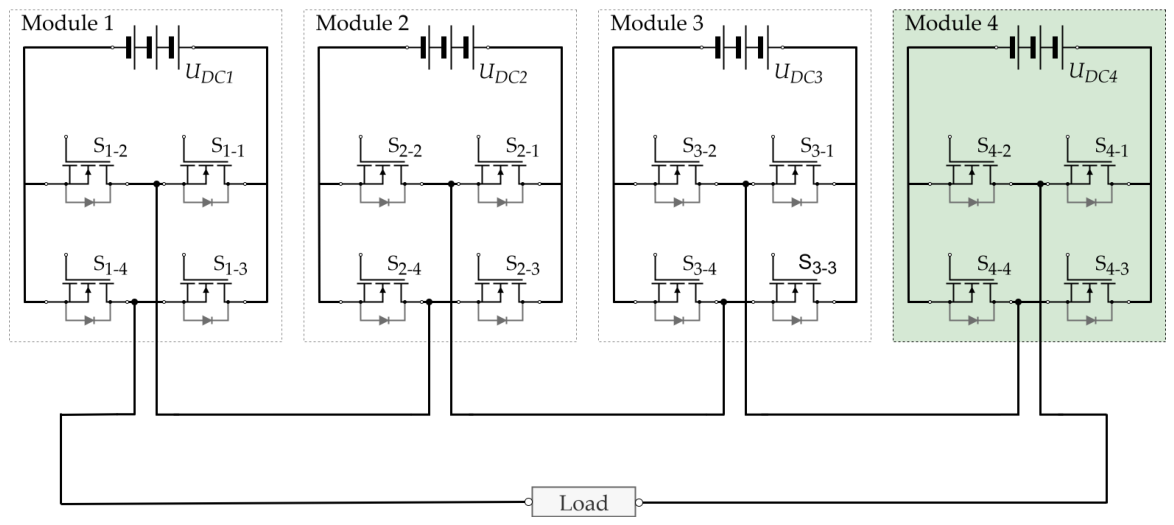
In this work, a four-module MMC topology with an integrated battery was used to enhance its redundant operation capabilities further. Under normal operation only three modules are active at any given time, while the fourth serves as a redundant spinning reserve. The spinning reserve serves as a shared role across all the modules in the system to equalize module usage and battery energy consumption. This function rotates during operation at a constant interval of a few seconds, depending on the system’s capacity. Each module contains a full-bridge circuit, a battery, and a microcontroller with measuring sensors, allowing it to operate independently of the rest of the system.
Figure 1 shows a basic schematic of the used topology, where
represents the battery voltage of module X, and
denotes transistor Y of module X, where Y is labeled from 1 to 4.
Under normal conditions a sorting algorithm assigns each module an operating role. This role determines the voltage level at which the module will contribute to the system’s output. The topology operates with a seven-level output voltage signal, utilizing three modules simultaneously in three roles. The module operating in role 1 generates the first voltage step, and it is active for the majority of the period. The module in role 2 generates the second voltage step, and it is active for less time than the module in role 1. The module in role 3 generates the third voltage step, and it is active the least during the period. Each operating role draws a different amount of energy from the battery. By changing the modules’ operating roles periodically, the sorting algorithm can balance the battery voltages of the modules, even if their capacities differ. Balanced battery voltages are required for a symmetrical system output. If the voltages drift apart, the output signal will distort, resulting in additional losses in the load. The fourth module, acting as a spinning reserve, is assigned operating role 0. This role is passive and contributes no energy to the system output. To maintain balanced voltages, role 0 is reassigned periodically to a different module simultaneously with the other three operating roles. New module roles are assigned based on the battery voltages. The module with the highest battery voltage receives operating role 1, as it drains the most energy during the sorting algorithm’s period. The module with the lowest battery voltage is assigned role 0, and it does not contribute energy in the next period. The remaining modules are assigned roles accordingly.
If a fault occurs in a module’s transistor, the sorting algorithm can disable the faulty module and continue operation with the three remaining modules. The faulted module is assigned operating role 0 permanently and remains passive. The system output signal will remain unchanged, but the battery energy of the faulted modules will become unavailable, resulting in a 25% reduction in system autonomy.
2.1. Improved Sorting Algorithm
The improved sorting algorithm proposed in [
11] can operate under a single transistor fault in a module without any loss of system autonomy. This is achieved by using the faulted module in half-bridge mode, preserving access to the battery’s energy. In half-bridge mode, a module can provide only a negative or positive output voltage, depending on the position of the faulted transistor. With a faulted module included in the MMC topology during operation, another healthy module must compensate for the missing output signal that the faulted module cannot generate. The improved sorting algorithm uses a four-module topology, in which two modules operate in half-bridge mode during redundant operation. This ensures that the output signal is equivalent to that produced by three fully healthy modules.
The operating role assigned to the faulted module is determined by its battery voltage, but only for the half-period of the output signal it can generate. The module compensating for the missing half-period is assigned the identical operating role. For this purpose, the module with the lower battery voltage is chosen, as it will consume the least amount of energy during the half-period, regardless of the assigned role. During redundant operation, role 0 is no longer used, and all the modules are active.
Using this algorithm, balancing module voltage levels becomes even more critical, as different modules are used for each half-period of the output signal. If the voltage levels begin to deviate, the output signal will not only become deformed, but it may also develop a DC offset. This can cause additional power losses in the load powered by this system.
2.2. Algorithms’ Drawbacks
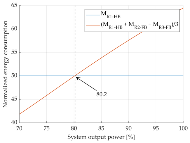
The improved sorting algorithm can operate under a single transistor fault without changes to the output signal or system autonomy, as long as the system operates within the constant power output limit. Theoretical analysis indicates that this limit occurs at 80.2% of the output power.
Figure 2 compares the average module energy consumption between one faulted and three normal modules. The faulted module operating in half-bridge mode using role 1 is labeled
. Role 1 is assigned to maximize the energy usage from the module’s battery. One healthy module operates with the identical assigned role during the opposite half-period, and it is also labeled
. The two remaining healthy modules operate in full-bridge mode with roles 2 and 3, labeled
and
, respectively. When the faulted module consumes more energy than the healthy modules on average, the balancing algorithm can adjust the module roles easily to compensate and maintain similar battery levels. Conversely, if the faulted module consumes less energy than the healthy modules on average, it becomes impossible for the improved sorting algorithm to maintain balanced battery voltages. A crossover point exists, which determines the power limit for long term operation system operation. Below this limit, the algorithm can maintain balanced battery voltages for all the modules, including the faulted module. When the system output power exceeds this limit, the faulted module’s voltage will diverge from the healthy modules gradually, leading to an increasingly asymmetrical multilevel output and distorted sine wave. When the output power falls below the limit, the module voltages re-balance, restoring a symmetrical multilevel output.
To overcome the limitation, an addition to the algorithm is proposed in this work. By accounting for differences in the module battery voltage levels during operation above the constant output power limit, the module operating times can be adjusted accordingly, maintaining an uncompromised sine-wave output. Using this method, the improved sorting algorithm can provide redundant operation without affecting the user, and with identical autonomy time. The module voltage levels will no longer limit the system output power output during redundant operation.
3. Voltage Level Compensation
If the MMC output voltage levels become unbalanced, the output sine wave will, consequentially, become distorted, and will no longer match the desired reference value. A voltages level compensation method is used in order to eliminate the deviations caused by the differences in the modules’ battery voltages. During converter operation, the modules’ battery voltages are monitored continuously by the sorting algorithm. The same measurements can be used for voltage level compensation when voltage differences occur. The voltage values are used in ratios to adjust the module operational limits, ensuring a continuous sine-wave output.
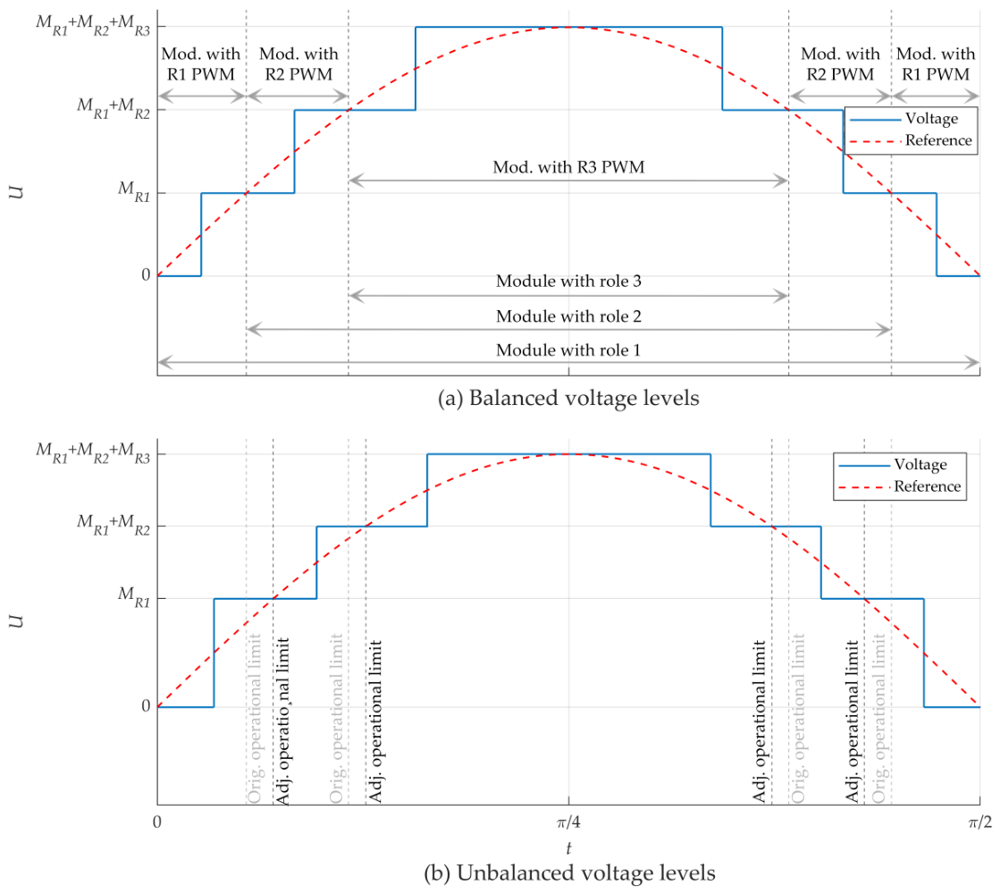
Figure 3 compares the module operational limit positions in a balanced and unbalanced scenario during the positive half-period of the output voltage signal. When the voltage levels differ, the reference limits are shifted, to compensate and maintain the sine shape of the output current. The module voltages are marked as
, representing a module’s battery voltage operating with role X. The presented system output voltage is theoretical and does not include PWM. When PWM is used, a module begins and ends its PWM regime within its operational limits. The PWM duty ratio is calculated to form a continuous sine wave in the systems output. In
Figure 3a, all the module voltage levels are identical. When the reference value crosses a module voltage level or a sum of levels, the next module is activated, and the system output voltage continues to rise during the rising quarter-period. The vertical limits indicate the module operational boundaries, and the module operation times are shown below the signal graphs. Each module can operate either in PWM mode or in a constant open state, with the PWM regimes indicated separately for each module.
Figure 3b presents an example of unbalanced voltage levels. The voltage of the module operating with role 1 was increased by 50%, creating a distortion in the system’s output current. With this voltage change, the intersection points with the reference signal were repositioned, adjusting the vertical operational limits. The module operation times are modified accordingly to compensate for the unbalanced voltages, preserving the output current waveform. Due to the increased voltage, the output current amplitude is higher, which can be adjusted further by lowering the reference value. For comparison, the original operational limits are shown in light gray.
Two examples of voltage level compensation are presented in the following chapters. First, an existing method for normal system operation is shown, where the output sine wave remains symmetrical regardless of the compensation. Second, the proposed voltage compensation algorithm is introduced, used for post-fault operation in combination with the improved sorting algorithm. This method accounts for different modules contributing to the positive and negative halves of the sine wave with different voltage levels, resulting in an asymmetrical output before compensation.
The voltage differences used in this article are extreme cases, and they are unlikely to occur in a real-world scenario. These exaggerated values help demonstrate the effects of voltage level differences visually. In practice, smaller voltage differences produce less noticeable waveform distortions, though the impact on the load remains.
3.1. Existing Method
The existing voltage compensation methods adjust the module operation times according to their voltage levels. This preserves the output current sine-wave shape and avoids changes to the load. To maintain the output current amplitude, the reference value is lowered accordingly.
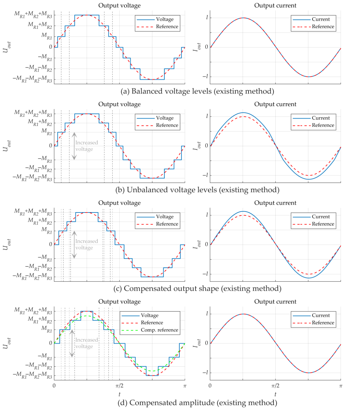
Figure 4 represents four scenarios with balanced and unbalanced voltage levels, along with the gradual compensation steps to conserve the original current output. In
Figure 4a the optimal voltage conditions are shown, with all the modules’ voltage levels balanced. The vertical lines indicate the module operational limits at the intersections of the reference value and module voltage levels. The original operational limits are included in gray for comparison across all the scenarios, highlighting how the reference intersections are repositioned during compensation relative to the balanced conditions. In
Figure 4b, the module providing the first voltage step has its voltage increased by 50%, resulting in unbalanced voltage levels. This causes the combined output voltage to rise, which increases the output current. In this scenario no compensation is applied, so the output current no longer matches the reference value. The current overshoots the reference due to the increased voltage, distorting the sine wave and increasing the signal’s THD. Such a distorted signal can affect the load negatively. The operational limits remain unchanged, and they no longer intersect the reference at the module voltage level. In
Figure 4c, the voltage level compensation method is applied, taking the ratio of the modules’ battery voltages into account. This repositions the operational limits to align with the intersections of the reference signal and module voltage levels. Compared to
Figure 4a, the module operating with role 1 experiences a greater shift in operational timing due to its increased voltage level. The other reference points are adjusted accordingly to preserve the optimal sine shape of the output current. The output signal is corrected to a pure sine wave, but the amplitude still overshoots the original reference value. In
Figure 4d, the reference amplitude is lowered to compensate for the increased module voltage, producing a new compensated reference, shown in green. This adjustment compensates the output current fully, which again matches the reference value, both in shape and amplitude.
3.2. Proposed Method
The improved sorting algorithm uses one additional module to achieve redundant operation without battery capacity loss. Under high output power, the voltage of the faulted module begins to deviate due to the limitations of the algorithm. This causes distortions similar to those shown in
Figure 4b. What is more, such distortions occur only in the positive or negative half-periods of the output signal, resulting in a DC offset. This prevents the existing voltage compensation methods from being applied, as they are intended for symmetrical unbalanced voltage with identical modules contributing to both halves of the signal.
To address this, a modified voltage compensation method is proposed, suitable for use with the improved sorting algorithm. This method eliminates the previous limitation on maximum output power under unbalanced voltages, enhancing the algorithm’s performance and usability. While module voltage imbalance may still occur, it no longer limits the maximum output power. At lower output power, the improved sorting algorithm continues to balance the module voltages normally. The proposed compensation method operates independently for the positive and negative half-periods of the system output current. First, the sine-wave voltage level compensation is calculated, to determine the module operational limits. These calculated limits are compared with the reference signal, to generate intersection points for module operational limit placement, and are normalized to match the reference signal amplitude. Voltage limit 0 is always 0 in (1), and voltage limit 3 is always 1 in (4). The voltage limit 1 is calculated in (2), where the voltage of the module operating with role 1,
, it is compared to the sum of all the operating modules’ voltages. This generates the operational limit between the modules with roles 1 and 2. Voltage limit 2 is calculated in (3), where the sum of the modules’ voltage operating with role 1 and 2,
and
, is compared to the total voltage sum, determining the operational limit between the modules with roles 2 and 3. These calculations are performed at each sorting algorithm execution interval, and repeated separately for the positive and negative half-periods, as different modules operate in each half-period. Second, the reference amplitude is adjusted for the half-wave with a higher voltage. It is reduced to match the half-period with the smaller voltage sum. Using (5), a ratio
is calculated for amplitude correction, depending on the polarity of the larger half-wave voltage sum, denoted as
for positive and
for negative half-periods. This correction is applied only to the corresponding half-period. Together, these two steps achieve full compensation, allowing the output current to remain unchanged across varying module battery voltages. All the symbols used are defined in
Table 1.
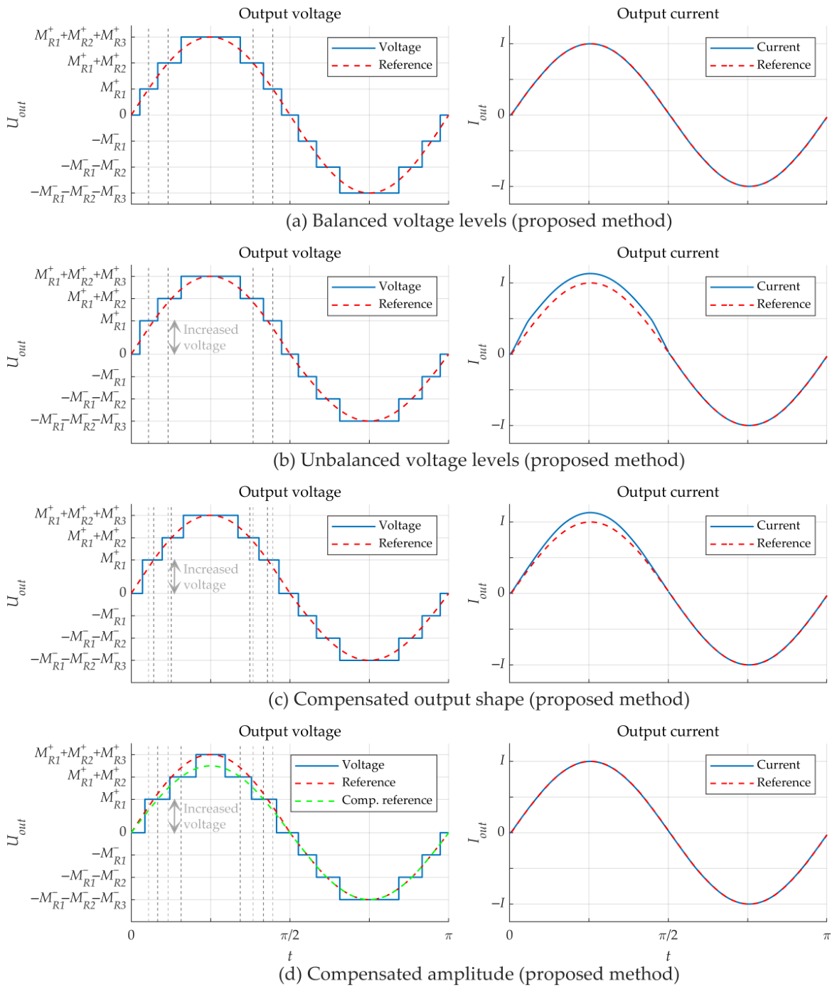
Figure 5 represents the same four scenarios and compensation steps as in the previous chapter, now combined with the improved sorting algorithm. The faulted module with higher voltage is used only in one half-period of the output current in this example, in the positive half-period. The compensation steps match those of the existing methods, but they are applied solely to the half-period containing the faulted module. In
Figure 5a, all the module voltage levels are identical, and the output current matches the reference. In
Figure 4b, the faulted module’s voltage increases by 50%. As it can generate only positive voltage in half-bridge mode, it contributes only during the positive half-period, causing an increased amplitude and distortion in that half of the output current. In
Figure 4c, the proposed voltage compensation method is applied only to the positive half-period, leaving the negative half-period unchanged. This adjusts the module operational limits and operating times to correct the output current waveform. Finally, in
Figure 4d, the reference amplitude is lowered for the positive half-period, completing the compensation. With these steps, the output current once again matches the reference perfectly, even with the faulted module having an increased voltage level.
4. Simulation Results
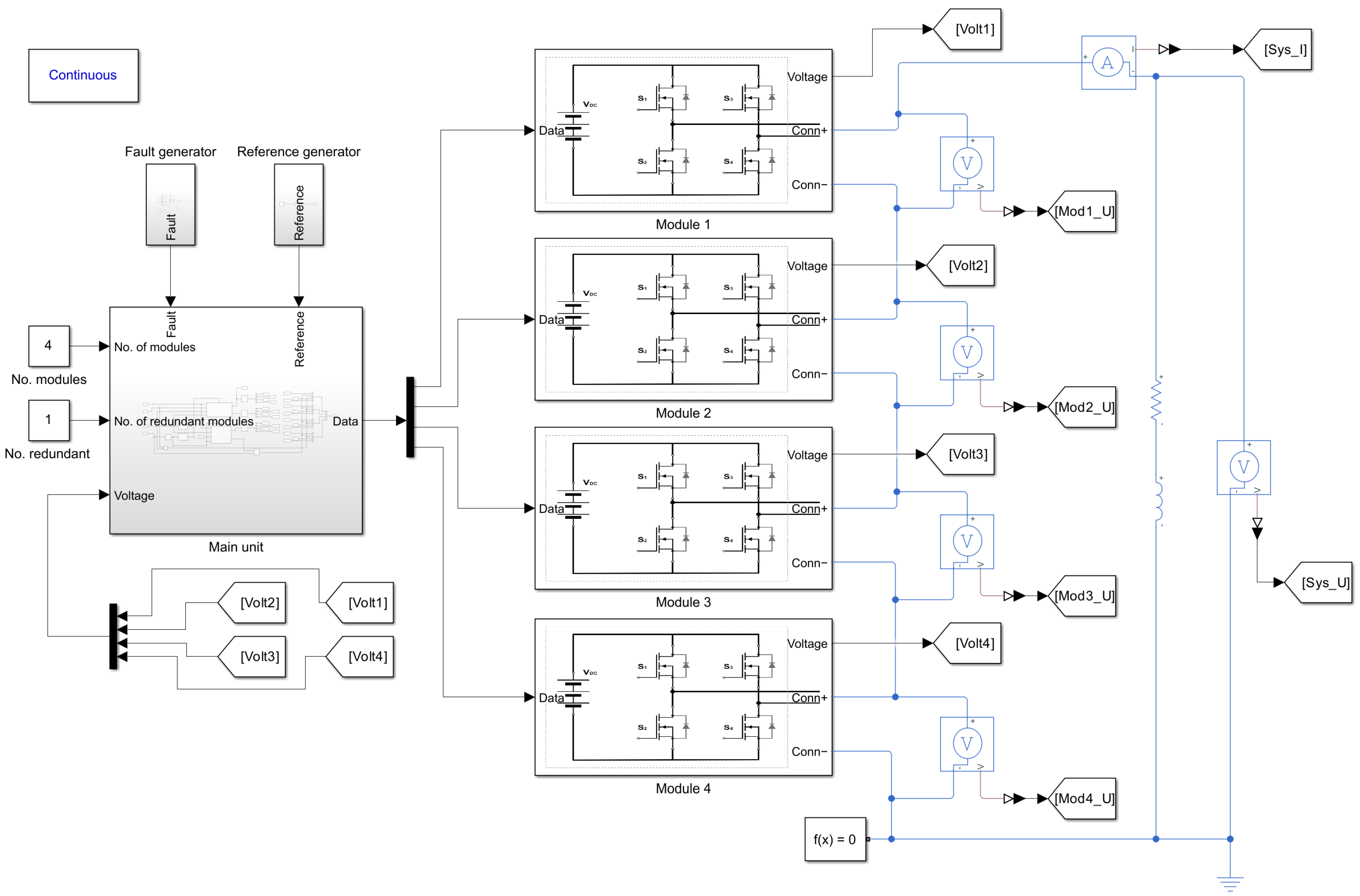
The proposed voltage compensation method was first tested in a simulation model created in Matlab 2021b, Simulink. The model simulates the operation of an MMC with an integrated battery and is presented in
Figure 6. It is composed of four modules, the main unit, a fault generator, and a reference generator. Each module includes a full-bridge circuit, a battery, and a PWM controller operating at 20 kHz. The PWM controller generates an appropriate control signal for the full-bridge circuit to produce a continuous sine-wave output current from all the modules combined. It takes into account the assigned role of the module and its operational limits, which are modified according to the voltage level ratios of the active modules at a given moment. The model also includes a main unit that gathers battery voltage information and module fault conditions, and executes the sorting algorithm to determine the module roles. The fault generator unit is used to generate a predetermined fault in a selected module at a chosen simulation time. The reference generator unit is a sine-wave generator with a frequency 100 Hz frequency and a scalable amplitude. The left side of the model represents the signal part, while the right represents the electrical part. The four modules operate independently, and they are connected in series to generate the combined output dictated by the main unit.
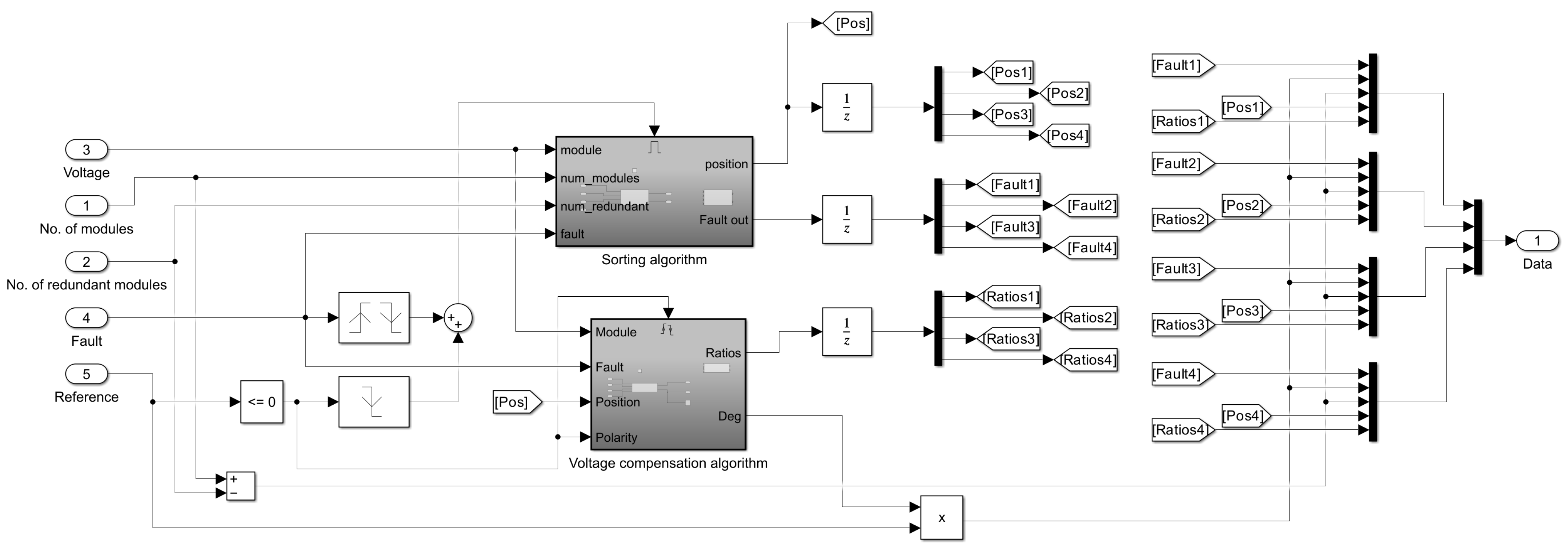
Figure 7 shows the structure of the main unit. It consists of the sorting algorithm and the voltage compensation algorithm. The sorting algorithm uses the module voltages and fault conditions to determine the module roles and balance their battery voltages optimally. When new module roles are determined, the voltage compensation algorithm is executed in addition. This algorithm calculates the new module operational limits and adjusts the reference signal to compensate for the different voltage levels. The voltage compensation algorithm is activated only when a faulted module is in operation. The sorting algorithm balances the healthy modules, and their voltages remain similar. When a faulted module is used, the sorting algorithm is executed at each period of the reference signal. In contrast, the voltage compensation algorithm is executed every half-period to update the module’s operational limits.
For the simulation tests a resistive–inductive load was used with 12 Ω and 610 μH. The module battery voltages were set to either 9 V or 12.6 V, depending on the test conditions. The batteries were modeled as fixed voltage sources without discharge effects. The proposed algorithm relies solely on voltage measurements to adjust the output current shape and amplitude at each execution. Therefore, the real battery discharge voltage curve does not affect its performance. The reference signal amplitude was kept at 100% throughout the simulations.
The simulation tests were performed three times under different conditions. Each simulation lasted 20 ms to display the two periods of the 100 Hz output signal clearly. Because fixed battery voltages were used, each signal period in the simulation is identical.
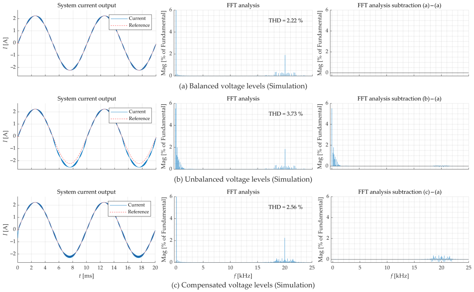
Figure 8 presents the results of the three simulation scenarios using different algorithms and module voltage levels. The first column shows the system output current together with the reference signal. Under optimal operation, the output current should follow the reference signal. The second column shows the FFT analyses of the output current up to 25 kHz. The third column shows the subtraction between the FFT result of the measured signal and the FFT result of
Figure 8a. This highlights the changes occurring in the different scenarios.
Balanced module voltage levels were used in
Figure 8a. All the modules had battery voltages of 9 V. In the first column, the output current follows the reference signal accurately. The FFT analysis in the second column shows a THD of 2.22%, with a clear spike at 20 kHz corresponding to the switching frequency. The third and fifth harmonics are negligible. In the third column, the FFT result is subtracted from itself, resulting in a zero-value graph. In
Figure 8b, the voltage level of one module was increased to 12.6 V. This module is faulty and can only generate a negative output voltage. Therefore, it is assigned operating role 1 and is used only during the negative half-period. The voltage compensation algorithm is not used in this scenario, so the output current derives from the reference value and no longer follows it correctly. Because of the improved sorting algorithm operation, only the negative half-period of the output current is affected. The FFT analysis in the second column shows that an increased current amplitude over only one half-period introduces a spike at 0 Hz, indicating a DC offset. The other harmonics are also increased significantly, and the THD rises to 3.73%. The subtracted FFT analysis in the third column highlights interference at lower frequencies due to the current distortion. Since the module switching strategy remains unchanged, the differences at higher frequencies near the switching frequency are negligible. The presented voltage compensation algorithm is applied in
Figure 8c. After adjusting the module operational limits and correcting the reference amplitude, the output current again follows the reference signal. The FFT analysis in the second column shows a reduced THD of 2.56%. The DC offset is eliminated, and the lower frequency harmonics are again negligible. A slight increase in harmonics near the switching frequency can be observed because the module switching strategy differs between the positive and negative half-periods. The subtracted FFT analysis in the third column confirms successful compensation, with no remaining lower frequency harmonic differences. Minor differences near the switching frequency remain, due to the modified switching strategy.
For a clearer comparison of the simulation results
Table 2 summarizes the values obtained from
Figure 8. The first column shows the FFT subtraction results for
Figure 8b up to 1 kHz, while the second column shows the corresponding results for
Figure 8c. This numerical comparison across the different frequencies validates the effectiveness of the voltage compensation algorithm.
The simulation results confirm the successful operation of the proposed voltage compensation algorithm. The FFT analysis of the third scenario shows that the system was compensated successfully, despite the uneven module voltage levels under fault conditions. The voltage of the faulted module was increased from 9 V to 12.6 V, a 40% increase, while the output current remained unchanged.
5. Experimental Results
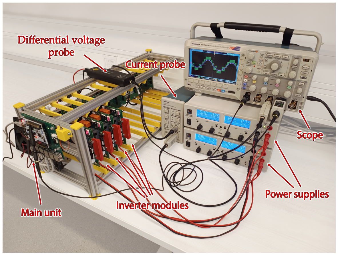
The proposed voltage compensation algorithm was also tested on an experimental system to verify its operation further. The system is an MMC with integrated batteries, designed for a maximum voltage of 12.6 V per module and a maximum current of 10 A. The modules were custom-designed to allow software modifications for testing the new operating methods. Each module contains an independent microcontroller, a measuring circuit, three 18650 Li-Ion batteries, and a full-bridge circuit. A rack was designed to hold the modules and connect them in series. A main unit was added, to collect the measured values from the modules, execute the sorting algorithm, and determine the operating conditions for each module. The main unit also receives current, temperature, and fault information to ensure that the system operates under safe conditions. The sorting algorithm used in this system operates with three modules simultaneously during normal operation out of the four available modules. The experimental setup is shown in
Figure 9. A single-phase operation was used for this test. Therefore, only active modules were populated for phase one. Modules with fully charged and nearly discharged batteries were used to achieve voltage level differences. Operating with nearly discharged batteries proved difficult when attempting to capture results with the desired voltage levels. When the system output was activated, a noticeable voltage drop across the batteries under load was observed, which did not match the simulation results. To resolve this issue and achieve comparable results, the batteries were replaced with four isolated power supplies, to ensure repeatable and stable results. Due to the proposed algorithm’s design, this simplification will not affect its performance. The system operation was captured using an oscilloscope with a differential voltage probe and a current clamp. The load used was of a restive–inductive type with 12 Ω and 610 μH, as in the simulation. The captured results were transferred to a PC and arranged into a presentable format without modifying the recorded signals.
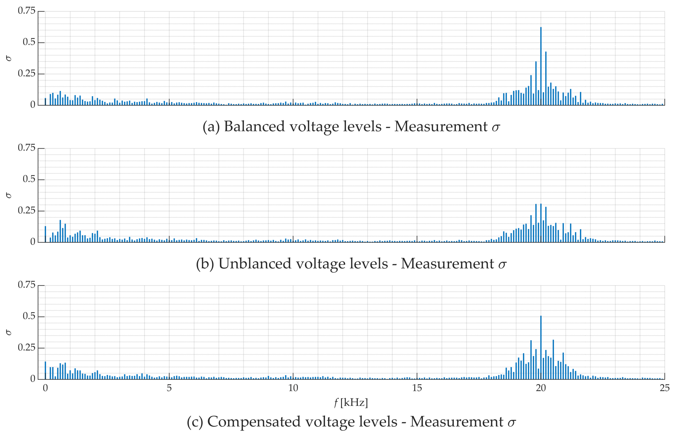
Continuous measurements from the experimental system showed slight deviations between the repeated results. These variations were caused by electrical noise present in both the system and the measurement equipment. To minimize this effect and obtain more accurate results, each measurement was repeated ten times and analyzed using an FFT. The average value of these measurements was then used as the final FFT analysis result. To validate the measurements further, the standard deviation of each frequency component was calculated, and it is presented in
Figure 10. Three graphs are shown, each representing the standard deviation of the FFT analysis for one of the three experimental scenarios presented later in
Figure 11. The results show low standard deviations across all the frequencies, indicating reliable measurements despite small differences between the samples. The largest deviations occurred near the switching frequency of 20 kHz, which is less critical than those near the fundamental frequency.
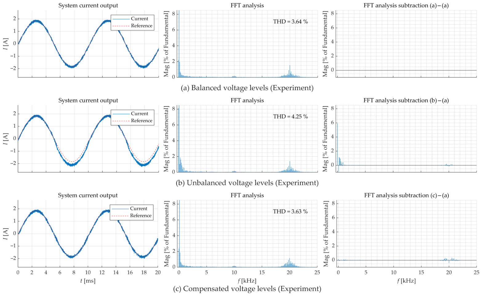
The experimental results are shown in
Figure 11. They are arranged identically to the simulation results to allow a clear comparison. In
Figure 11a, the test was performed with all the module voltage levels set to 9 V. The first column shows the output current following the reference signal closely. The FFT analysis in the second column shows a calculated THD of 3.64%. Some measurement noise is visible near the fundamental frequency of 100 Hz and near the switching frequency of 20 kHz. The third column shows the FFT subtraction result, which is empty in this case, since the signal is subtracted from itself. In
Figure 11b, a fault is introduced in one module, forcing it to operate in half-bridge mode and producing only a negative voltage during the negative half-period. The voltage level of this module was also increased to 12.6 V. This resulted in a higher current amplitude and distortion in the negative half-period of the output waveform, similar to the simulation results. The FFT analysis in the second column shows a THD value of 4.25%. Increased noise in clearly visible near the fundamental frequency. A large spike is also present at 0 Hz, indicating a DC offset in the signal. Because the module with the higher voltage operates only during the negative half-period, this imbalance introduces a DC offset in the output signal. The third column shows the FFT subtraction between
Figure 11a,b. A large difference is visible at 0 Hz, and noticeable differences are present near the fundamental frequency. Since the module switching strategy remained unchanged in this scenario, no significant changes are visible near the switching frequency. These results match the simulation results closely. In
Figure 11c, the proposed voltage compensation algorithm was used on the experimental system. The output current shown in the first column again followed the reference signal closely, despite one module having an increased voltage level. The FFT analysis in the second column shows a THD of 3.63%. Compared to
Figure 11b, the noise near the fundamental frequency is reduced significantly. Slight differences appeared near the switching frequency, due to the modified module switching strategy. The third column shows the FFT subtraction between
Figure 11b,c. A significant improvement is observed near the fundamental frequency, where the difference was nearly zero. A small difference appears near the switching frequency due to the altered switching strategy. This result confirms the successful operation of the proposed voltage compensation algorithm and matches the simulation results closely.
For clearer comparison of the experimental results,
Table 3 is presented and arranged identically to
Table 2 used for the simulation results.
Figure 11b,c are compared for frequencies up to 1 kHz. The numerical comparison confirms the effectiveness of the proposed voltage compensation algorithm in the experimental system. The noise introduced by the increased module voltage level was compensated nearly completely.
6. Discussion
The proposed voltage level compensation algorithm was first verified theoretically to mitigate the operational limitations of the improved sorting algorithm. The theoretical principle is based on the existing methods for compensating different voltage levels in a symmetrical output current. The voltage limit calculation is defined by four equations, two of which have fixed values, and are used to determine the modules’ operational limits. A fifth equation is introduced to compensate for the asymmetrical amplitude caused by the differing voltage levels. This approach results in a fully compensated output current that, theoretically, matches the original waveform.
The simulation tests were performed using a model of a modular multilevel converter with an integrated battery, consisting of four modules. Three tests were conducted, where the first served as a control case under ideal conditions with identical module voltage levels. In the second test, an increased voltage level was introduced in the faulted module, resulting in distortion of the output current signal. In the final test, the proposed voltage level compensation algorithm was applied, eliminating the distortion from the output current signal completely. The measurements were compared using an FFT analysis. The FFT result of the first test served as the reference. In the second test, increased noise is observed near the fundamental frequency, along with a DC offset. In comparison, the third test shows a significant improvement relative to the first, with both the noise near the fundamental frequency and the DC offset eliminated effectively. These results confirm the successful operation of the proposed algorithm in a simulation environment. A slight difference in noise remains near the switching frequency, due to the modified module switching strategy.
For final validation of the algorithm, experimental tests were conducted using a custom-built MMC with integrated batteries consisting of four modules. The experiments were performed under the same conditions as the simulation tests to enable direct comparison of the results. To obtain reliable measurements, each test was repeated multiple times, and the results were averaged. The three experimental scenarios correspond to those used in the simulation. By applying the proposed voltage level compensation algorithm to the experimental system, the output current was fully compensated, even when operating with a faulted module at an increased voltage level. These results confirm the successful operation of the proposed algorithm in an experimental setup.
The presented results were obtained under steady-state operation, demonstrating the successful performance of the proposed algorithm. In real-world applications, the batteries are subjected to dynamically changing loads, which cause rapid variations in voltage and reduce the accuracy of the proposed algorithm’s voltage measurements. The simplest solution is to use an average of multiple measurements over a defined time period. Since the algorithm is executed at intervals of several seconds, sufficient time is available to obtain a reliable average measurement. To improve accuracy further, the voltage measurements can be replaced with more precise SOC estimations.
The presented voltage level compensation algorithm can be applied to an MMC with any number of modules per phase. If more than four modules are used and one operates in a faulted half-bridge mode, the output current distortion decreases as the number of modules increases. The proposed algorithm remains applicable, and the output signal can be maintained after compensation, however, it is primarily intended for topologies with a lower number of modules. As the number of modules increases, the difference between the distorted and compensated output current becomes progressively less noticeable. This work focuses on the application of the algorithm in single-phase operation. When extended to a three-phase system, the algorithm can be applied independently to each phase. Additionally, the reference current value must be adjusted separately for each phase, to achieve identical output current amplitudes under fault conditions during high-power operation.
7. Conclusions
This paper focuses on the further improvement of post-fault operation of an MMC with integrated batteries using the improved sorting algorithm. The targeted application are EVs where uncompromised redundancy and the ability to achieve the destination even if an internal transistor fault occurs in one module per output phase is desirable. The previous work presented the improved sorting algorithm, which was able to maintain similar voltage levels across all the modules, including the faulted one, but only to a certain power output. In operations above 80.2%, the algorithm was unable to discharge the faulted module sufficiently, which caused distortion in the output current signal. In this work, an additional voltage level compensation algorithm was developed to mitigate this drawback.
The proposed algorithm achieves output signal distortion compensation by adjusting the module operational times and the reference signal for each half-wave of the output signal. This method was proven successful in the simulation and experimental test results. The algorithm uses voltage measurement of the module battery levels for operation, and it is unaffected by the battery discharge curve. Fixed voltage sources were used to achieve a better result comparison between the simulation and experimental tests. The simulation and experimental results are comparable, and they indicate a significant improvement when the proposed algorithm is applied in an unbalanced module voltage level scenario. The simulation results indicate a THD increase from 2.22% to 3.73% when the faulted module voltage is increased by 40%. When the proposed algorithm is used, the THD value is corrected to 2.56%. An important indication is the DC offset present in the output signal. Before the use of the proposed algorithm, a 5.91% magnitude of the fundamental frequency was measured, presented in
Table 2. After compensation, the same value was reduced to 0.16%. The experimental results show comparable values. When the faulted module voltage was increased, a THD rise was indicated from 3.65% to 4.25%. After compensation, the same value was reduced to 3.63%. The DC offset was also reduced from 5.52% of the magnitude of the fundamental frequency to 0.01%, presented in
Table 3, proving the algorithm’s successful operation.
By implementing the proposed algorithm, the existing constant high power output limit present in post-fault operation is eliminated using the improved sorting algorithm. This presents a substantial benefit for electric vehicle performance under high load in post-fault operation, limited to a single transistor fault in one module per output phase. The proposed algorithm can be scaled to a system with any battery type and capacity operating with different power outputs. The proposed algorithm’s benefits are most noticeable in a system with a low number of modules. It can be used with any number of modules, but the effect of the algorithm will become gradually less noticeable.
Future research could focus on extending the system to three-phase operation and applying the developed algorithms to balance the module voltage levels. In a three-phase system, an additional challenge would be balancing the module voltages between phases while maximizing the utilization of stored battery energy and minimizing the unused energy remaining in the system after shutdown. Future goals also include using a simulated driving profile to represent real-world dynamic load conditions with real batteries used. This would verify the algorithm’s usefulness in different vehicle types and driving profiles.