1. Introduction
With the advancement of the marine industry, a wide range of transducers has been introduced. Most transducers are based on piezoelectric elements, and their electrical equivalent models typically consist of a capacitor in parallel with multiple RLC circuits [
1,
2,
3,
4]. The resonant frequencies represented by the RLC model correspond to the frequency bands where the transducer exhibits optimal sound pressure levels, while at other frequencies, the transducer behaves primarily as a capacitive load. Conventional amplifiers may experience instability or oscillation when driving capacitive loads, and they require substantial reactive current during signal reproduction. Although transducer manufacturers have released dedicated amplifiers to drive such devices, they often emphasize high output power and large current delivery capabilities to accommodate transducers with highly frequency-dependent impedance characteristics. However, these amplifiers rarely provide information regarding their Total Harmonic Distortion (THD) performance [
5,
6,
7,
8,
9,
10,
11,
12].
In general, a PWM amplifier employs an output inductor–capacitor (LC) filter to suppress switching noise. To achieve a flat frequency response, the inductance and capacitance values of the LC filter are designed based on the load resistance R, targeting a damping factor (
) close to 0.707 [
13,
14,
15,
16,
17]. However, when a step-up transformer is added to apply a voltage higher than the PWM amplifier’s output to a piezoelectric transducer, constraints arise in the design of the output LC filter. From the primary side of the transformer, the equivalent capacitance of the piezoelectric element increases proportionally to the square of the turn ratio, while the equivalent resistance decreases inversely with the square of the turn ratio.
To obtain a desired reproduction frequency band, once the cutoff frequency is determined, the inductance of the output filter is dictated by the increased equivalent capacitance of the piezoelectric sensor. Under these conditions, the damping factor determined by the resulting inductance, capacitance, and resistance becomes less than 0.707, leading to a boosted frequency response near the LC cutoff frequency. In order to maintain a flat response across the reproduction band, the cutoff frequency must be set higher. However, this compromises the attenuation of switching frequency components, necessitating a trade-off in cutoff frequency selection.
Furthermore, if the harmonic frequencies of the reproduced signal fall within the boosted frequency range, these harmonics are amplified, resulting in increased THD. This paper discusses methods to address these issues and presents the corresponding results.
The amplifier developed in this study is designed to reproduce marine biological sounds (e.g., dolphin vocalizations) using PWM techniques. The target frequency range is from 2 kHz to 20 kHz, with a goal of maintaining THD below 1%. The system is powered by a 100 V battery, aiming to deliver an output voltage of 200 V to the transducer. To enhance system efficiency, the switching frequency was set to 200 kHz.
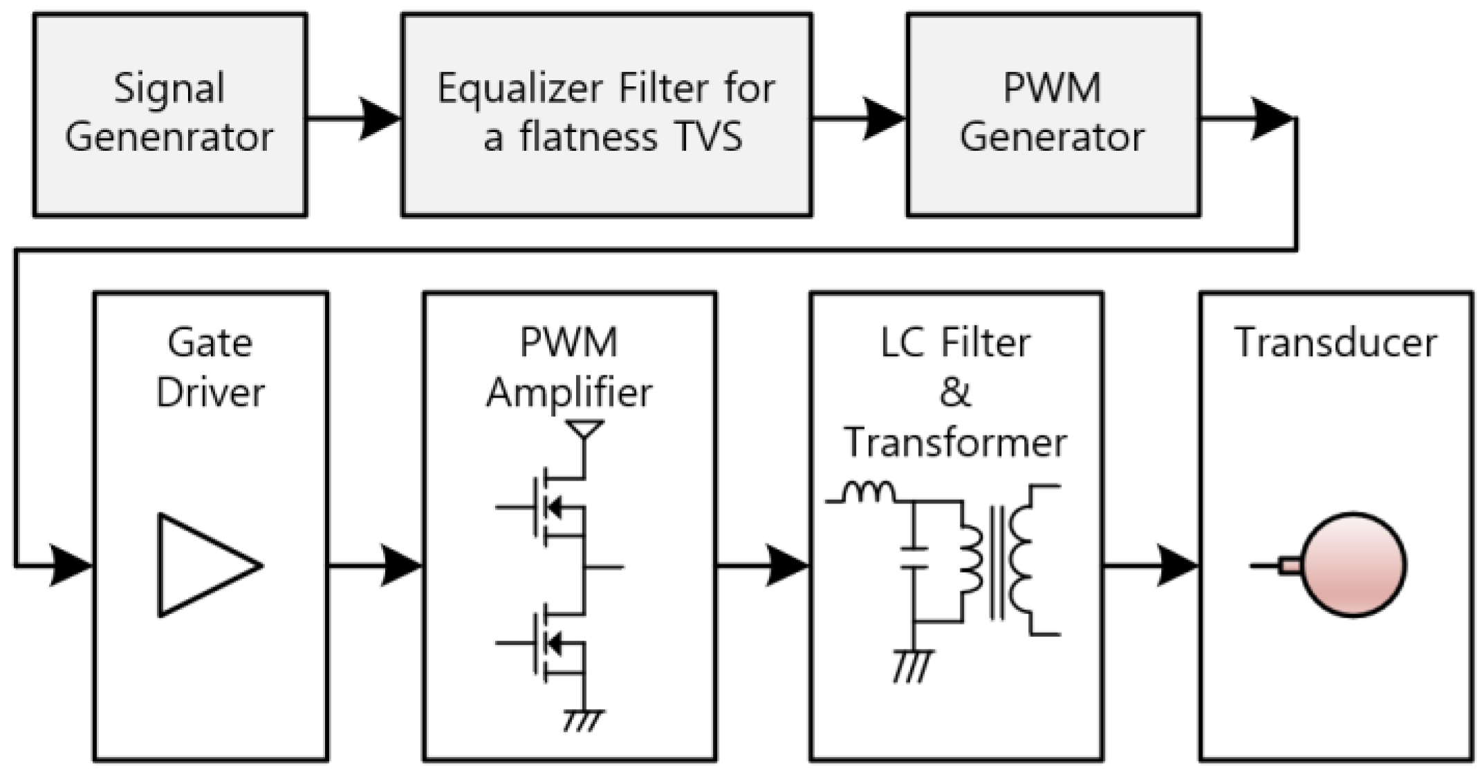
Figure 1 illustrates the configuration of the transmitter system developed in this study. Piezoelectric transducers typically produce maximum sound pressure at their resonant frequency, while output levels decrease at other frequencies. Therefore, an equalizer filter is required to ensure uniform sound pressure across the entire frequency band. In this system, the equalized signal is converted into a PWM signal, which drives the Class-D amplifier via a gate driver to generate high-power PWM output. The high-frequency switching components are removed by an LC filter, and the transmission signal is then increased through a step-up transformer before being radiated as an acoustic signal via the transducer.
This paper focuses exclusively on the modeling of the step-up transformer and the transducer, excluding the signal generator, the equalizer filter, and the PWM generator, and discusses filter design and THD improvement methods based on these models.
2. Component Modeling and Output Filter
To optimize the design of the LC filter and step-up transformer located at the output stage of the PWM amplifier, the impedance characteristics of both the step-up transformer and transducer were measured. Based on these measurements, equivalent models were constructed for the PSPICE simulator, a circuit simulation program used on personal computers. This section provides a detailed description of the modeling process.
2.1. Transducer Modeling
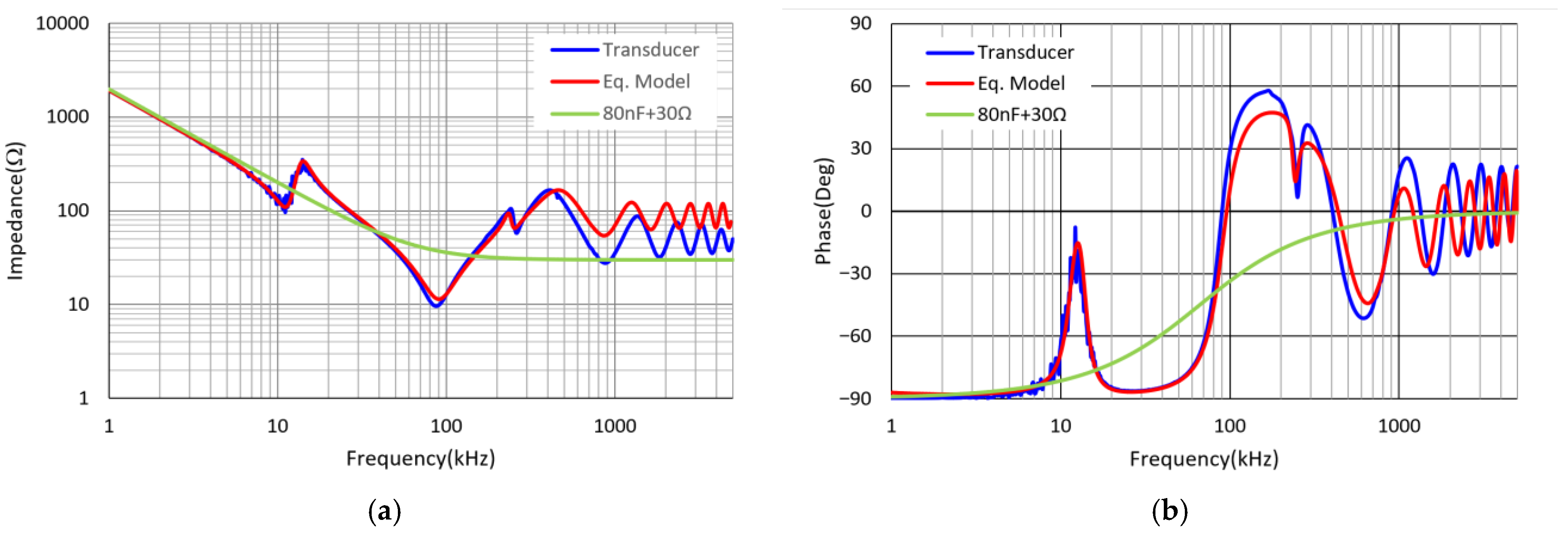
The blue line in
Figure 2a shows the measured impedance characteristics of the GeoSpectrum M18C-6.0 transducer (GeoSpectrum Technologies Inc., Dartmouth, NS, Canada) connected with a 100 m cable [
4].
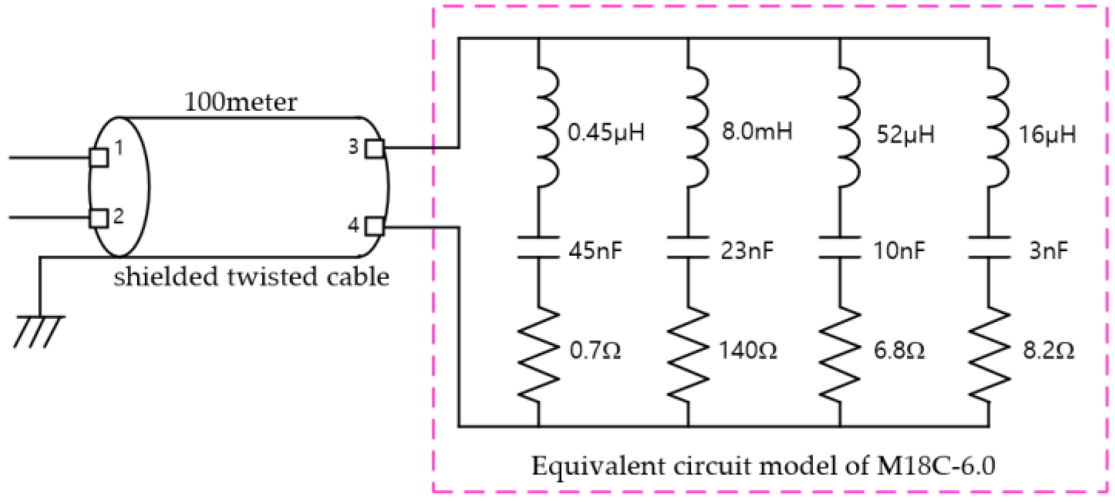
Figure 2b’s blue line shows the measured phase degrees. Based on these measurements, equivalent models of the twisted cable and transducer were extracted for simulation, as illustrated in
Figure 3. The twisted cable model in
Figure 3 was constructed by connecting 100 units of the model in
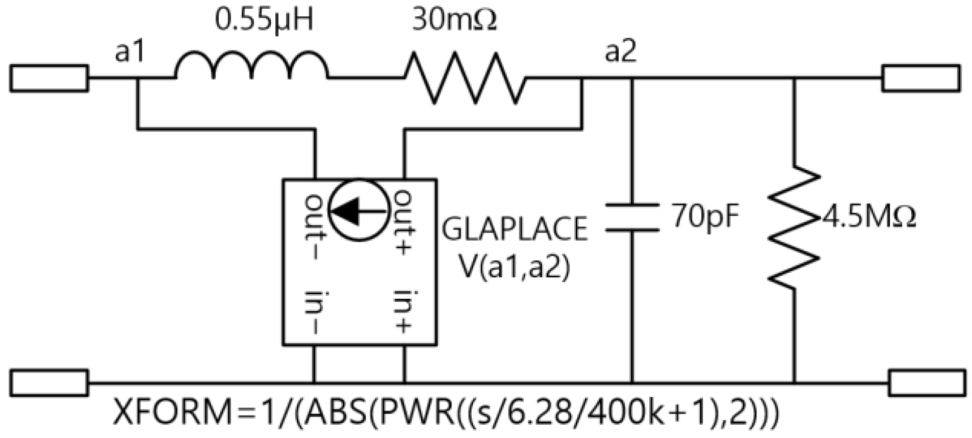
Figure 4 in series.
Figure 4 presents the equivalent impedance model for a 1 m segment of the cable.
The red lines in
Figure 2a,b present the simulation results of impedance and phase characteristics based on the equivalent model shown in
Figure 3. In
Figure 4, GLAPLACE is a built-in PSPICE function implemented as a voltage-controlled current source. Connected in parallel with the 0.55 μH inductor and the 30 mΩ resistor, this GLAPLACE element serves as a frequency-dependent resistance model that accurately captures the variation in resistance caused by the skin effect at higher frequencies. In the frequency range above 1.5 MHz, noticeable discrepancies are observed between the simulated and measured impedance and phase responses, particularly near the resonant frequency. This deviation is attributed to the frequency-dependent variation in the dielectric constant of the cable insulation, which affects the overall capacitance. Since the equivalent model used in this study does not incorporate a frequency-dependent capacitance representation, modeling errors occur at higher frequencies.
2.2. Step-Up Transformer
The amplifier operates with a supply voltage of 100 V, and the PWM transmitter generates a maximum output of approximately 70 Vrms. To achieve the target acoustic pressure of 194 dB re 1 μPa/m at the transducer, an output voltage of approximately 210 Vrms is required. Accordingly, the nominal turns ratio of the step-up transformer is 1:3; however, considering step-up transformer losses, the actual turns ratio was set as 1:3.03.
Given that the lowest playback frequency is 2 kHz, the secondary-side magnetizing inductance of the step-up transformer must be greater than the transducer impedance at 2 kHz, requiring at least 78.2 mH due to the 81 nF capacitance of the transducer. Similarly, the primary-side inductance must be no less than 8.5 mH.
Since leakage inductance directly affects the performance of the output LC filter, it must be minimized during step-up transformer design. In conventional winding methods—where the secondary winding is placed over an insulation layer after the primary winding—the magnetic coupling is relatively weak, resulting in leakage inductance values that are a fraction of a few hundredths of the magnetizing inductance. To address this issue, a sandwich winding technique was employed to minimize leakage inductance.
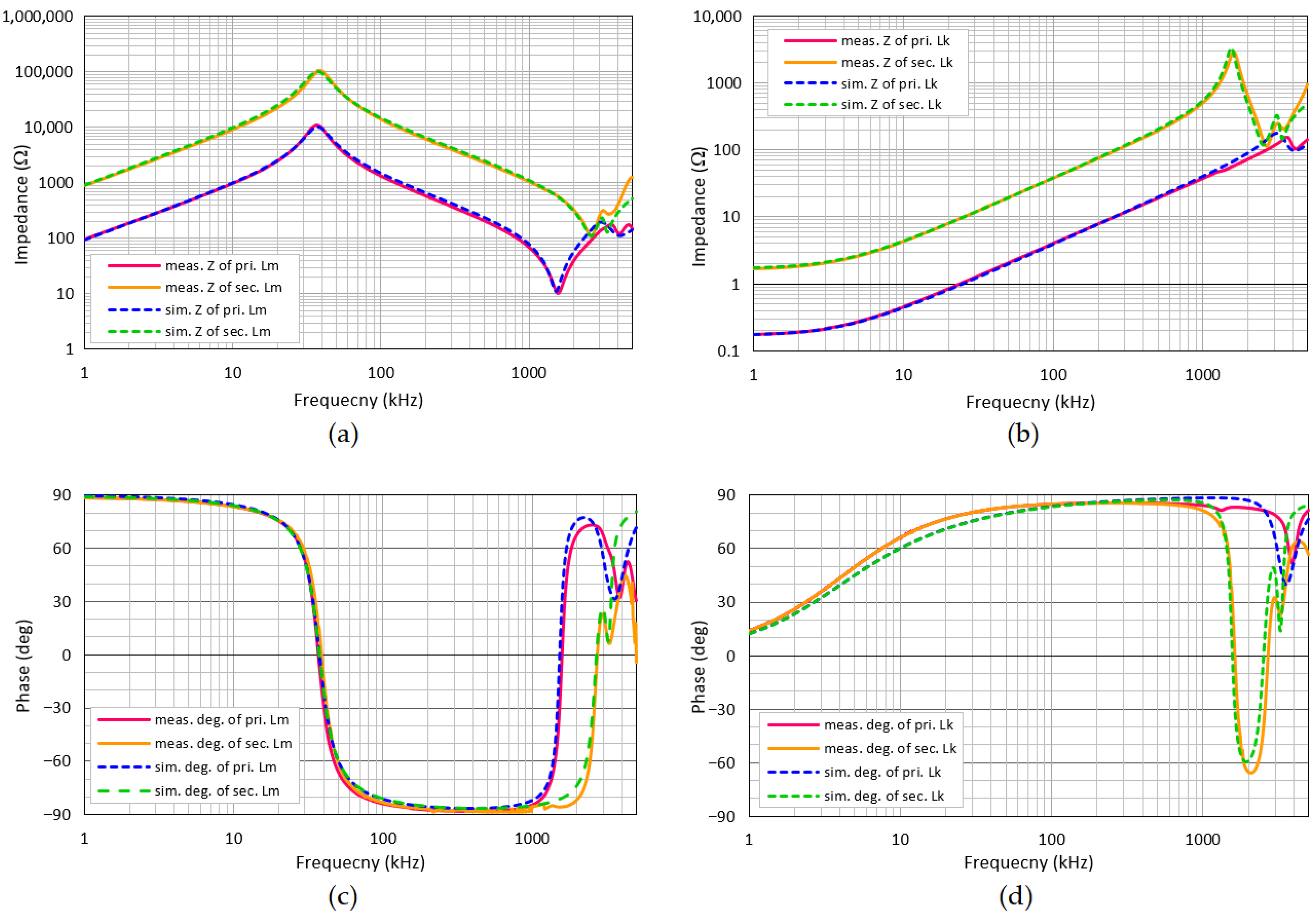
As a result, the prototype step-up transformer achieved a primary and secondary magnetizing inductance of 16 mH and 147 mH, respectively, and a primary and secondary leakage inductance of 7.2 μH and 67.9 μH. The step-up transformer core consists of two parallel amorphous cut C cores (AMCC0100) [
18].
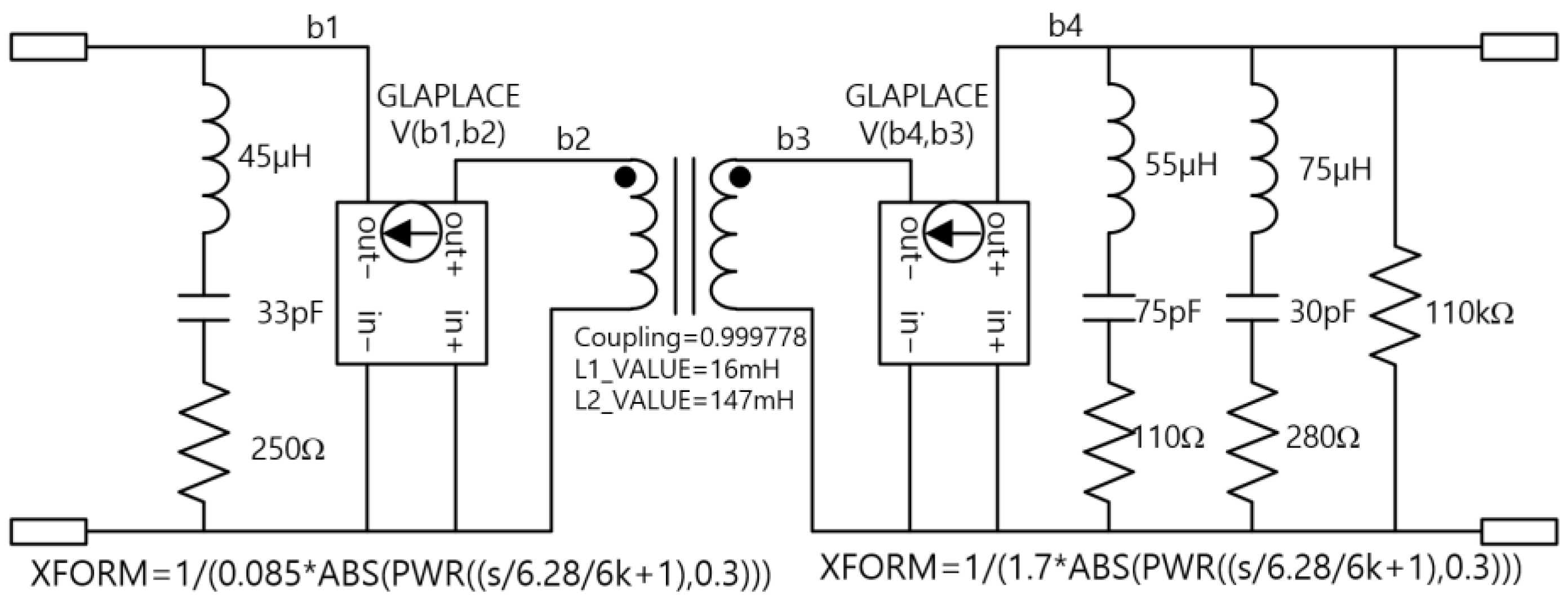
Based on these measurements, the equivalent model of the step-up transformer was constructed, as shown in
Figure 5. Solid lines in
Figure 6 show the measured impedance and phase characteristics of both the magnetizing and leakage inductances, and the dotted lines in
Figure 6 represent the simulation results of the impedance and phase characteristics derived from the model presented in
Figure 5. The close agreement between the measured data and the simulation results confirms the validity and accuracy of the proposed step-up transformer model.
2.3. Output LC Filter
According to the impedance measurements of the transducer shown in
Figure 2, the impedance decreases monotonically with frequency in the range of 1 kHz to 80 kHz, except near 12 kHz. The phase remains close to −90°, indicating capacitive behavior. This region can be modeled as an 80 nF capacitor. At frequencies above 100 kHz, the impedance drops approximately to 30 Ω, and the phase approaches 0°, suggesting resistive behavior. Therefore, the transducer can be simply modeled as a series combination of an 80 nF capacitor and a 30 Ω resistor, as represented by the green line in
Figure 2.
The simplified model of the transducer connected to the secondary side of the step-up transformer can be reflected to the primary side as approximately 0.72 μF + 3.3 Ω. The value is used as the effective output capacitance of the LC filter.
The primary function of the LC filter is to recover switching energy from the PWM output. The cutoff frequency (
fc) of the LC filter is typically set to 2–3 times the upper limit of the playback frequency. In this study, the cutoff frequency was set to 60 kHz, three times the upper playback frequency of 20 kHz. Using a capacitance of C = 0.72 μF and applying Equation (1), the required inductance L is calculated to be 9.8 μH.
Since the PWM output uses an H-bridge configuration, each output terminal is connected to two 4.9 μH inductors, and the ends of these inductors are connected to the primary side of the step-up transformer, completing the PWM output stage. However, due to the step-up transformer’s coupling coefficient being less than 1.0, leakage inductance exists on the primary side. Electrically, this leakage inductance is connected in series with the two 4.9 μH inductors. Therefore, if the leakage inductance reaches 9.8 μH, the two discrete output inductors can be omitted and replaced by the step-up transformer’s leakage inductance.
This configuration electrically connects the primary side of the step-up transformer directly to the H-bridge output terminals. As previously mentioned, sandwich winding was employed to achieve a leakage inductance close to the target value of 9.8 μH, resulting in a measured value of 7.2 μH. Since the leakage inductance is sensitive to the winding geometry, the measured value of 7.2 μH was used directly.
According to Equation (1), the cutoff frequency is calculated to be 69.9 kHz. However, when applying a coupling factor of 0.999778 for the step-up transformer, the simulation result yields a cutoff frequency of 59 kHz, which matches the design target. The green lines in
Figure 7a,b represent this result.
2.4. Switching Devices
PWM signals convey information through the ratio of high (H) and low (L) durations. Therefore, it is important to select switching devices with matched rise and fall times. While conventional PWM amplifiers typically use metal oxide semiconductor field-effect transistors (MOSFETs), this study employed Silicon Carbide Field-Effect Transistors (SiC FETs), which offer significantly faster switching speeds [
19,
20].
In this experiment, the switching device used was the UJ4C075023K4S from Onsemi (Scottsdale, AZ, USA) [
21]. This SiC FET provides fast rise/fall times of less than 25 ns and an exceptionally low reverse recovery time of 13 ns, resulting in switching losses that are approximately five times lower than those of traditional MOSFETs. Considering the reverse recovery time, the dead time was set to a reduced value of 30 ns, shorter than that used with MOSFETs.
The gate driver used was UCC23313BDWYR from Texas Instruments (Dallas, TX, USA), which features identical rise and fall times of 28 ns and matched delay times of 105 ns [
22]. These characteristics help suppress PWM signal distortion and maintain output waveform linearity. Thus, the combination of balanced switching devices and gate drivers ensures accurate PWM signal transmission and efficient system operation.
Therefore, the system achieves accurate PWM signal transmission and high-efficiency operation through the combination of a switching device and gate driver with balanced rise/fall characteristics and a minimized dead time.
2.5. Simulation of Frequency Characteristics
Figure 7 presents the simulated frequency and phase response of the system when driven by a 100 V DC source. The simulation incorporates the switching delay of the gate driver and FET, as well as the equivalent models of the step-up transformer and transducer. The green line in
Figure 7 shows that the system maintains a flat response up to 20 kHz. A resonance peak caused by the output LC filter and load appears at 59 kHz, with a boost of 7.1 dB compared to the flat-band response at 5 kHz. Attenuation at the switching frequency of 200 kHz is approximately expected to be −7 dB lower than that at the 5 kHz band. To achieve additional attenuation at 200 kHz region, an LCR notch filter was connected in parallel to the secondary side of the step-up transformer. The notch filter was tuned to resonate at the switching frequency of 200 kHz by L = 15 μH, C = 39 nF, and R = 1, and the damping factor (
) was set to 0.025. The resulting frequency response is shown as the cyan line in
Figure 7. By applying this notch filter, an additional attenuation of −25.0 dB was achieved at 200 kHz. Furthermore, the second and third harmonic components of the switching frequency were attenuated by −12.3 dB and −12.6 dB, respectively. Due to the influence of the notch filter, the resonance frequency shifted downward to 53.3 kHz. At this new resonance point, the gain increased by 10 dB compared to the flat-band response at 5 kHz.
3. Experimental Results and Improvements
3.1. First Experimental Result
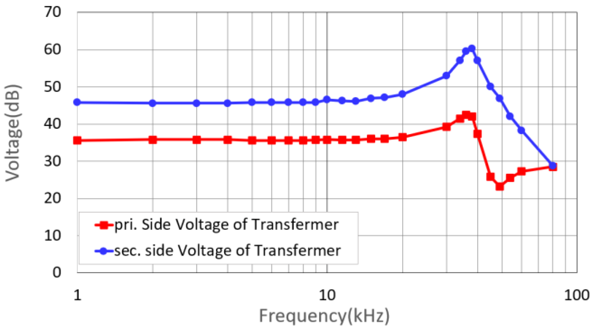
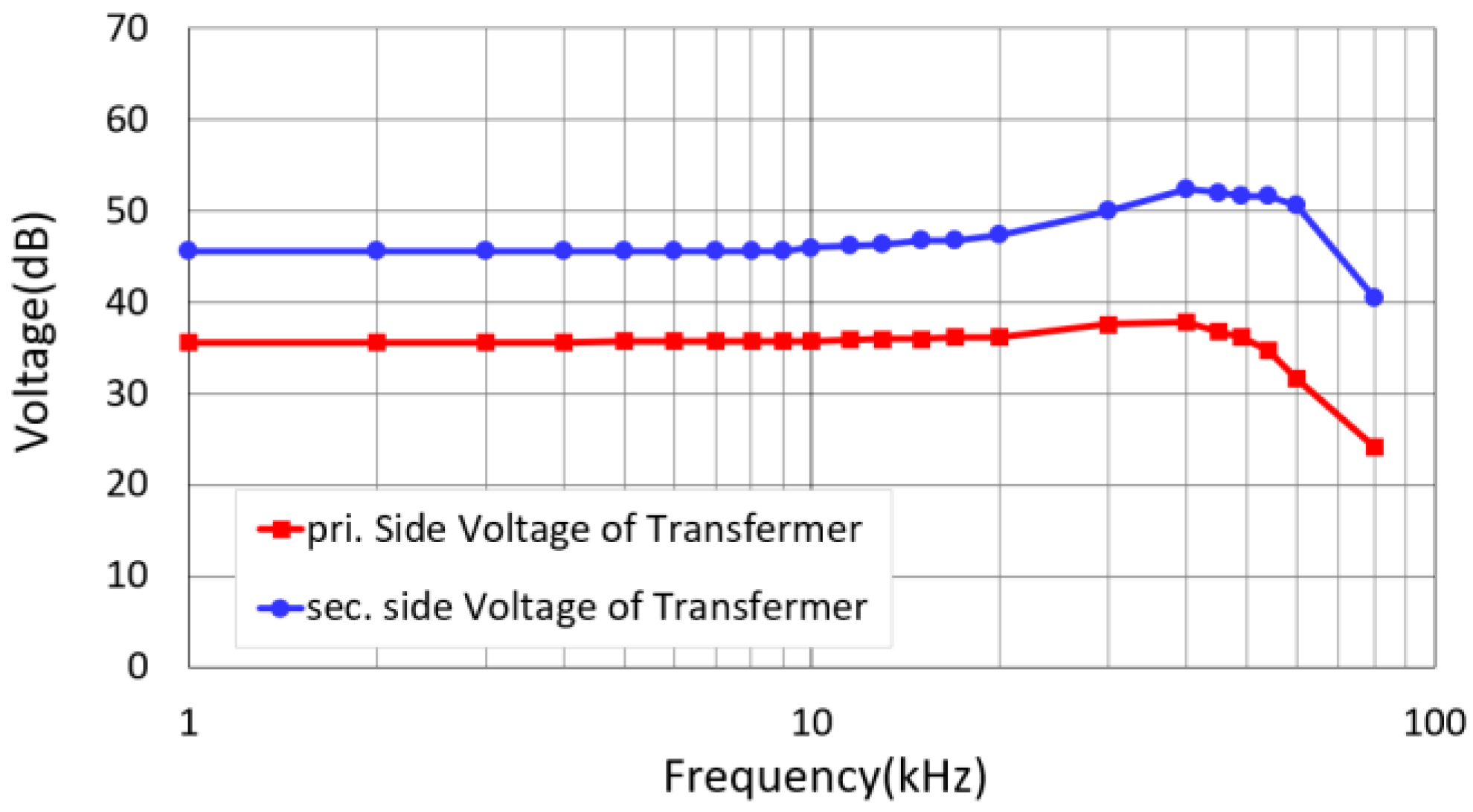
Figure 8 shows the frequency response of the amplifier measured at the secondary side of the step-up transformer with the transducer as the load. The measurement was conducted up to 80 kHz, which is near the Nyquist frequency of the switching frequency. The results indicate a flat response up to 20 kHz and a resonance boost of 12 dB at 50 kHz, which is 2.3 dB higher than the simulation prediction. This outcome is believed to be due to the model’s omission of the core nonlinearity of the step-up transformer. As shown in
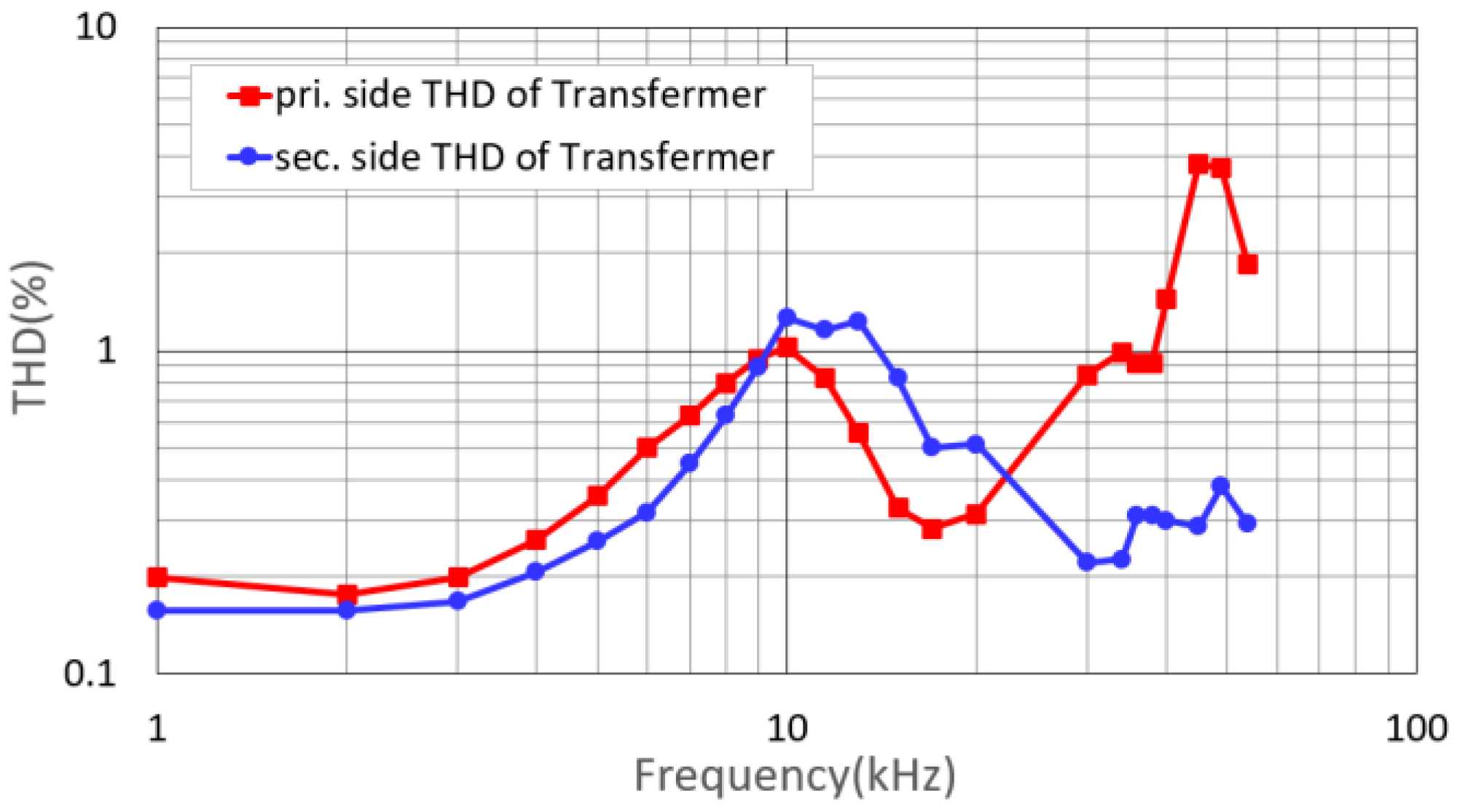
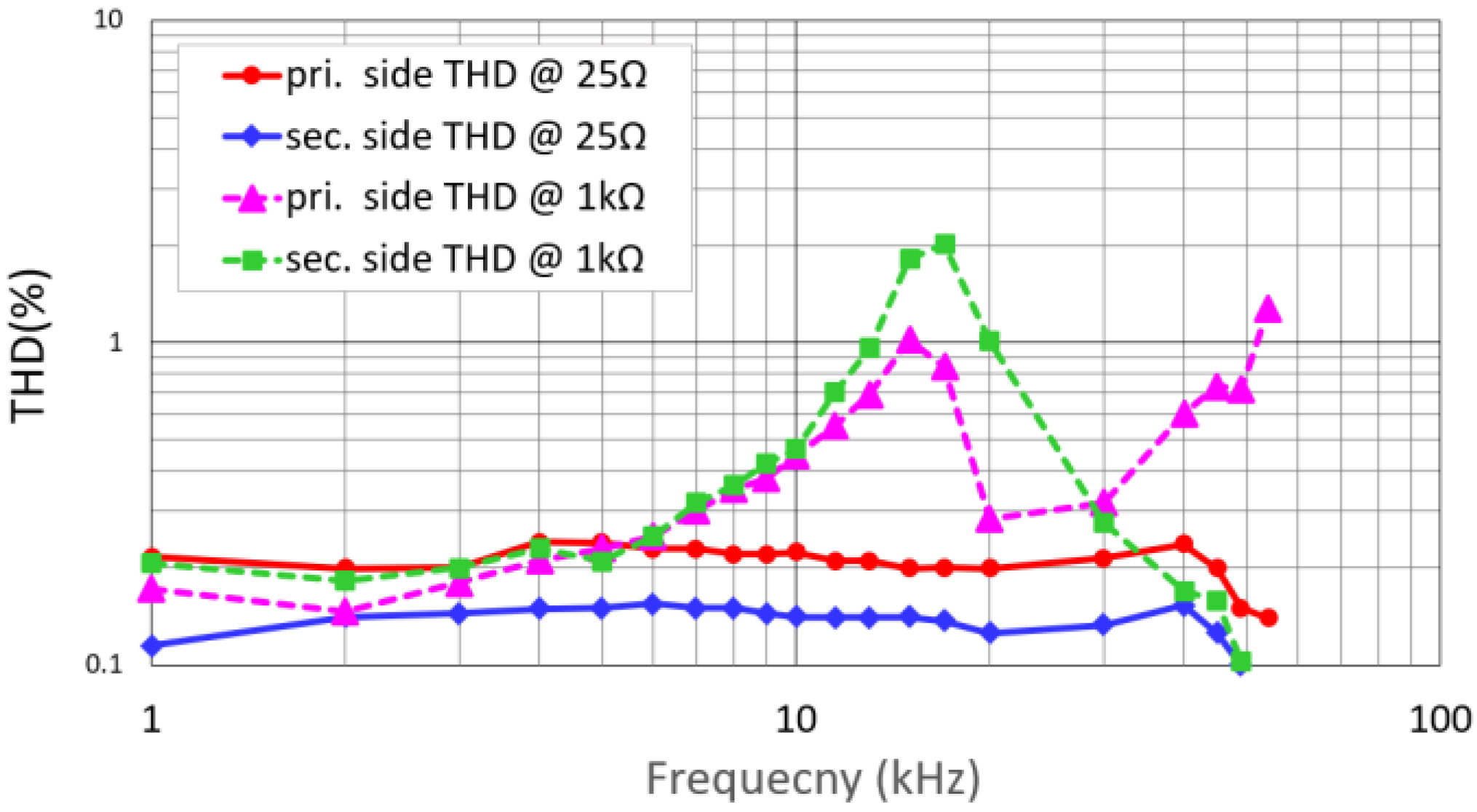
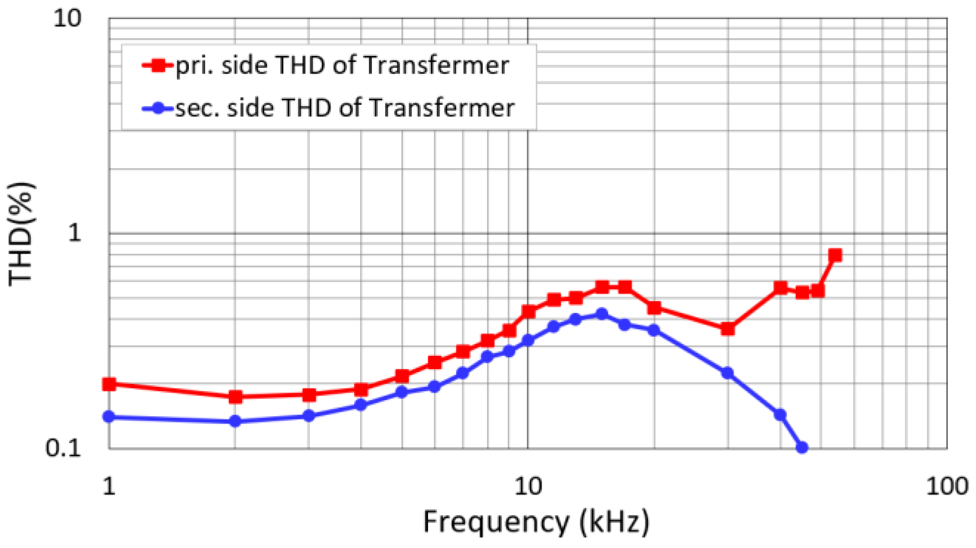
Figure 9, the THD exceeds 1% on the primary side of the step-up transformer in the frequency range around 45 kHz to 50 kHz, while on the secondary side, it surpasses 1% in the range of 10 kHz to 15 kHz.
According to the cyan simulation trace in
Figure 7, the attenuation at the switching frequency (200 kHz) is 32 dB lower than that at the 5 kHz band. As shown in the experimental waveform of
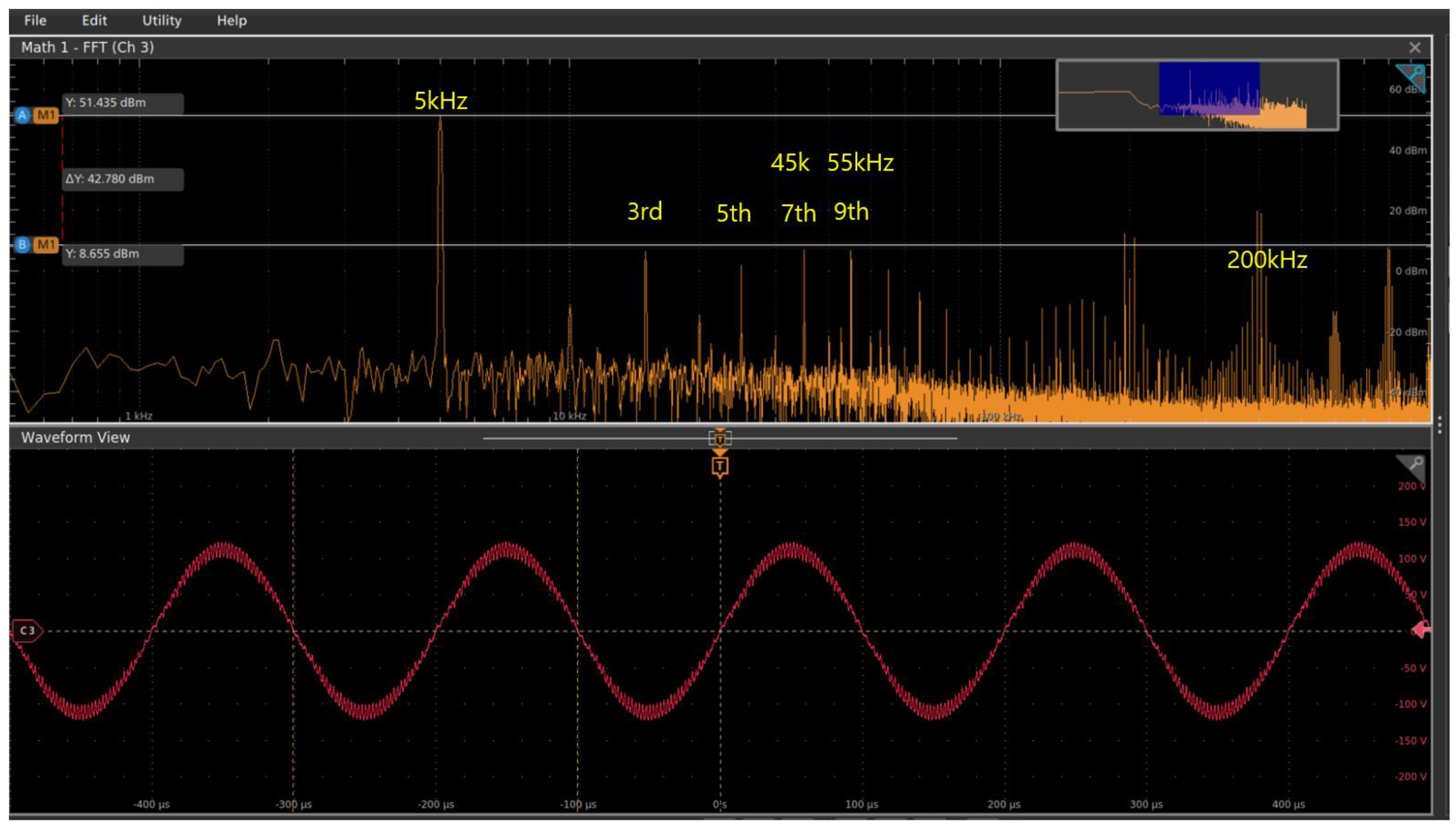
Figure 9, the amplitude of the 200 kHz switching frequency is 32.3 dB lower than that of the 5 kHz signal, indicating that the transducer and step-up transformer models were accurately designed and closely match the actual behavior.
3.2. THD Characteristics and Cause Analysis
To eliminate variability caused by the frequency-dependent impedance of the transducer, a fixed resistive load of 25 Ω was used. Secondly, to achieve a flat frequency response between the LC filter and the load resistor, the damping factor was set to 0.707. Based on this condition, the capacitor value of the LC filter was experimentally chosen as 56 nF, which is close to the calculated value of 52 nF.
As shown by the solid line in
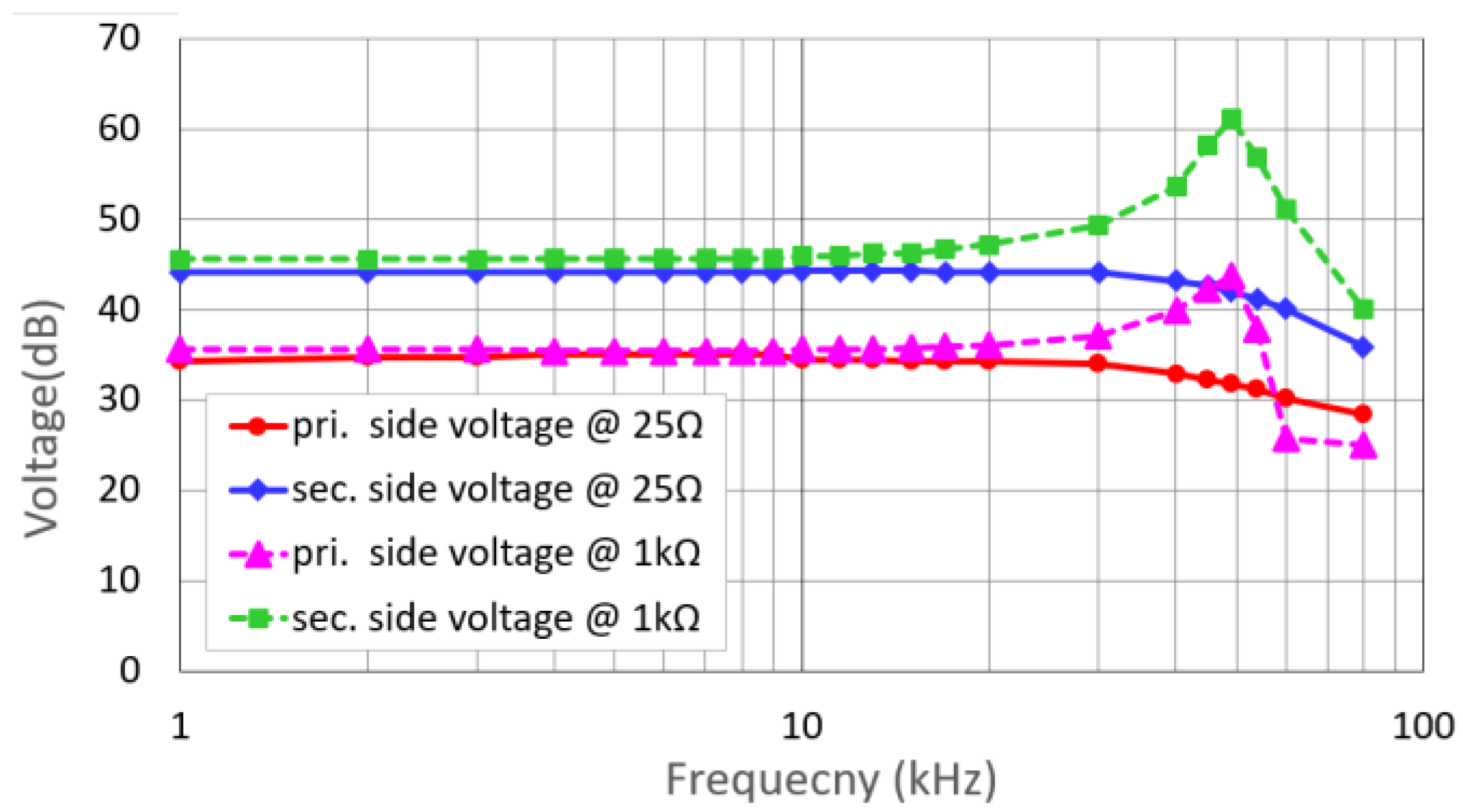
Figure 10, the frequency response under the 25 Ω load demonstrates a flat gain characteristic across both the primary and secondary sides of the step-up transformer. The solid line in
Figure 11 shows the THD characteristics under the same conditions, indicating the secondary sides of the step-up transformer achieved favorable THD levels of lower than 0.15%.
In contrast, the dotted lines in
Figure 10 and
Figure 11 show the measurement results when the LC filter value was fixed, and the load was changed from 25 Ω to 1 kΩ. The dotted line in
Figure 10 shows a 15 dB gain boost around the 50 kHz region when the load was 1 kΩ. The dotted line in
Figure 11 represents the THD characteristics when the load was 1 kΩ. In this case, the THD near 17 kHz worsened by a factor of five compared to the 25 Ω load. Typically, THD increases with higher current through semiconductors or passive components. However, in this case, even though the current flowing through the output FET and the step-up transformer decreased, the THD increased. If the increased THD were caused by the inherent nonlinearity of the device, degradation would be expected across all frequencies. However, since it occurs only at specific frequencies in this case, it is presumed to result from circuit-related characteristics such as component interactions or resonances.
This phenomenon is attributed not to the nonlinearity of the SiC FET switching waveform or the step-up transformer itself, but rather to the resonant peak behavior of the LC filter. When outputting a 17 kHz signal, a small third harmonic component (approximately 51 kHz) generated by inverter operation and the mild nonlinearity of the step-up transformer coincides with the resonant frequency formed by the output inductor and load capacitance. As a result, the third harmonic is boosted by 12 dB from its original amplitude, leading to degradation in THD at the fundamental frequency of 17 kHz.
The measured resonance frequency of the amplifier is 52 kHz, and the degradation of THD near 17 kHz, which is one-third of the resonance frequency, is consistent with this analysis.
Figure 12 presents the fast Fourier transform (FFT) result of a 5 kHz signal. Although harmonic amplitudes typically decrease as the harmonic order increases, the 7th and 9th harmonics—located near the 50 kHz region—appear larger than the 5th harmonic due to the gain boosting effect around that frequency.
3.3. THD Improvement Method
A common approach to improving THD is to apply negative feedback [
13]. However, in this system, the frequency and phase characteristics are influenced by a second-order pole from the output LC filter and time delays caused by the gate driver and FET switching. As shown in
Figure 7, the system lacks a gain margin, and the phase exceeds 180°, making it unstable for feedback control.
Inserting a proportional–integral (PI) amplifier to increase loop gain would introduce additional phase shift, resulting in a third-order pole system and further complicating feedback implementation. Moreover, the target frequency band for THD improvement is near 17 kHz. Designing a feedback loop with unity gain at a frequency approximately 3.14 times lower than the switching frequency (i.e., 63 kHz = 200 kHz/π) would not provide sufficient loop gain to effectively reduce THD at 17 kHz.
Therefore, instead of applying feedback, a notch filter was introduced to suppress THD. The degradation of THD near 17 kHz is attributed to the boost characteristics in the 45 k~50 kHz range, which corresponds to the third harmonic of 17 kHz. To reduce gain in this region, an LCR notch filter was connected in parallel with the load. The filter was tuned to resonate at 49.8 kHz by L = 0.6 mH, C = 17 nF, R = 68 Ω, and the damping factor was set to 0.18 by adjusting the resistance value to suppress the boost effect.
Although adjusting the LC ratio can yield a flatter frequency response when outputting signals above 15 kHz, the power dissipated in the notch filter’s resistor exceeds the power delivered to the transducer, while the reduction in THD does not scale proportionally. Therefore, the damping factor was selected by considering the trade-off between power consumption and THD suppression. The final results of this approach are presented in
Figure 13 (frequency response) and
Figure 14 (THD characteristics).
By connecting the notch filter in parallel with the secondary side of the step-up transformer, a flat frequency response was achieved up to 20 kHz, and a satisfactory result was obtained with the THD of the voltage supplied to the transducer reduced to 0.4%.
4. Conclusions
In this study, a sonar-based underwater transmitter capable of operating across a wide frequency range from 2 kHz to 20 kHz was designed. To achieve a flat frequency response and optimized THD, precise modeling and optimized design were conducted for each system component.
By measuring the impedance and phase characteristics of the transducer —including a 100 m cable—and step-up transformer and constructing accurate PSPICE models, the output LC filter was designed and analyzed. This enabled the design of the output LC filter and revealed both the gain peaking around the 50 kHz region and the insufficient attenuation in the switching frequency region.
To address these issues, two notch filters were applied, resulting in a −6 dB improvement in harmonic distortion near 15 kHz and a −32.3 dB enhancement in attenuation at the switching frequency region.
This research confirms the frequency boosting problem caused by the capacitive load characteristics of typical underwater transducers in PWM amplifiers with a step-up transformer and proposes an effective solution. The findings contribute not only to improving the performance of underwater acoustic amplifiers in wideband sonar transmission systems but also to reducing the design complexity of power amplifiers and enhancing overall system reliability.
Author Contributions
Conceptualization, M.P. and H.-g.W.; Methodology, M.P. and H.-g.W.; Software, B.K.; Validation, M.P. and H.-g.W.; Formal analysis, J.H.J.; Resources, H.-g.W.; Data curation, H.-g.W.; Writing—original draft, M.P.; Writing—review & editing, B.K. and J.H.J.; Visualization, M.P., B.K. and J.H.J.; Supervision, B.K. and J.H.J.; Project administration, B.K. and J.H.J. All authors have read and agreed to the published version of the manuscript.
Funding
This work was supported by the Korea Research Institute for Defense Technology (KRIT) Planning and Advancement Grant funded by the Korean government (DAPA—Defense Acquisition Program Administration) in 2022 (No. KRIT-CT-22-056, Acoustic Sensor Detection Technology Based on Marine Biological Sounds Research Laboratory).
Institutional Review Board Statement
Not applicable.
Informed Consent Statement
Not applicable.
Data Availability Statement
The data presented in this study are available upon request from the corresponding author. These data are not publicly available because they are part of an ongoing study.
Conflicts of Interest
Authors Minyoung Park, Byoungkweon Kim, Hyoung-gyun Woo and Jae Hoon Jeong were employed by the company SYSCORE Inc.
References
- Pyun, J.Y.; Kim, Y.H.; Park, K.K. Design of Piezoelectric Acoustic Transducers for Underwater Applications. Sensors 2023, 23, 1821. [Google Scholar] [CrossRef] [PubMed]
- Moaaz, A.; Yasin, M.; Khaliq, A.; Ali, S. Realization of Broadband Impedance Matching Networks for Enhancing the Performance of Underwater Surveillance Systems. J. Electr. Syst. 2019, 15, 392–404. [Google Scholar]
- Zhou, H.; Huang, S.H.; Li, W. Electrical impedance matching between piezoelectric transducer and power amplifier. IEEE Sens. J. 2020, 20, 14273–14281. [Google Scholar] [CrossRef]
- GeoSpectrum Technologies Inc. M18C-6.0 Transducer Specifications. Available online: https://www.geospectrum.ca/catalog/commercial/transducers/spherical-transducers/ (accessed on 17 April 2024).
- Benthowave Instrument Inc. Available online: https://www.benthowave.com/products/poweramplifier.html (accessed on 17 April 2024).
- Instrument Inc. Available online: https://instrumentsinc.com/linear-switching-amplifiers-and-sensors (accessed on 16 October 2025).
- Geospectrum Technologies Inc. Available online: https://geospectrum.ca/product-category/commercial/systems/ (accessed on 17 April 2024).
- Lee, B.-H.; Baek, J.-E.; Kim, D.-W.; Lee, J.-M.; Sim, J.-Y. Optimized Design of a Sonar Transmitter for the High-Power Control of Multichannel Acoustic Transducers. Electronics 2021, 10, 2682. [Google Scholar] [CrossRef]
- Yan, S.H.; Ming, W.; Guang, D.C.; Chao, D.H. Design and Implementation of a Class D Power Amplifier for a Transmitter in a Sonar System. In Proceedings of the International Industrial Informatics and Computer Engineering Conference (IIICEC 2015), Xi’an, China, 10–11 January 2015. [Google Scholar]
- Bhushan, A.P.; Manoj, G.; Sreedevi, K.; Gopal, V. Simulation Study of Linear Power Amplifier for Underwater Imaging Sonar Applications. In Proceedings of the 7th International Conference on Advances in Computing & Communications, ICACC 2017, Cochin, India, 22–24 August 2017. [Google Scholar]
- Schmidt, A.M.; Schmidt, J.H.; Kochańska, I. Suitability of Acoustic Power Amplifiers as Power Amplifiers in Underwater communication systems. Int. J. Electron. Telecommun. 2024, 70, 831–838. [Google Scholar] [CrossRef]
- Panchalai, V.N.; Kuncham, S.K.; Natarajan, K.; Ramesh, R. Review on Underwater Sonar Power Amplifier Technologies. In Proceedings of the 2024 IEEE Space, Aerospace and Defence Conference (SPACE), Bangalore, India, 22–23 July 2024; pp. 103–107. [Google Scholar]
- Jeong, J.H.; Cho, G.H. A high efficiency and wide bandwidth class D switching audio power amplifier with improved output stage and current mode control. Int. J. Electron. 1997, 82, 533–554. [Google Scholar] [CrossRef]
- Tang, B.; Geng, J.; Zhou, C.; Ouyang, H. Design of a High Efficiency Class-D Audio Power Amplifier. In Proceedings of the 2020 International Conference on Artificial Intelligence and Electromechanical Automation, Tianjin, China, 26–28 June 2020. [Google Scholar]
- Mei, S.; Hu, Y.; Xu, H.; Wen, H. The Class D Audio Power Amplifier: A Review. Electronics 2022, 11, 3244. [Google Scholar] [CrossRef]
- Jiang, X. Fundamentals of Audio Class D Amplifier Design: A review of Schemes and Architectures. IEEE Solid-State Circuits Mag. 2017, 9, 14–25. [Google Scholar] [CrossRef]
- Prakash, K. Power Amplifier for Sonar Application. IETE J. Educ. 1993, 34, 195–206. [Google Scholar] [CrossRef]
- Proterial. AMCC_0100. Available online: https://hilltech.com/products/power_components/amor_cores/amor_chart_std_core.html (accessed on 9 October 2025).
- Roscoe, N.M.; Zhong, Y.; Finney, S.J. Comparing SiC MOSFET, IGBT and Si MOSFET in LV distribution inverters. In Proceedings of the IECON 2015-41st Annual Conference of the IEEE Industrial Electronics Society, Yokohama, Japan, 9–12 November 2015; pp. 000743–000748. [Google Scholar]
- Biela, J.; Schweizer, M.; Waffler, S.; Kolar, J.W. SiC versus Si—Evaluation of potentials for performance improvement of inverter and DC–DC converter systems by SiCpower semiconductors. IEEE Trans. Ind. Electron. 2010, 58, 2872–2882. [Google Scholar] [CrossRef]
- On Semiconductor. UJ4C075023K4S SiC FET Data Sheet. Available online: https://www.onsemi.com/products/discretes-drivers/mosfets/sic-mosfets/uj4c075023k4s (accessed on 14 March 2023).
- Texas Instruments. UCC23313BDW Data Sheet. Available online: https://www.ti.com/product/UCC23313 (accessed on 14 March 2023).
| Disclaimer/Publisher’s Note: The statements, opinions and data contained in all publications are solely those of the individual author(s) and contributor(s) and not of MDPI and/or the editor(s). MDPI and/or the editor(s) disclaim responsibility for any injury to people or property resulting from any ideas, methods, instructions or products referred to in the content. |
