Article

Design and Implementation of an L-Band 400 W Continuous-Wave GaN Power Amplifier

1
School of Electronic Science and Engineering, University of Electronic Science and Technology of China, Qingshuihe Campus, Chengdu 611731, China
2
Southwest China Research Institute of Electronic Equipment, Chengdu 610036, China
3
The 13th Institute of China Electronics Technology Group Corporation, Shijiazhuang 050051, China
*
Author to whom correspondence should be addressed.
Electronics 2026, 15(1), 203; https://doi.org/10.3390/electronics15010203 (registering DOI)
Submission received: 23 November 2025 / Revised: 20 December 2025 / Accepted: 25 December 2025 / Published: 1 January 2026
(This article belongs to the Special Issue RF/Microwave Integrated Circuits Design and Application)

Abstract

Based on a large-signal chip model, this paper designs and implements an L-band broadband continuous-wave 400 W high-efficiency power amplifier fabricated using 0.5 μm GaN High Electron Mobility Transistor (HEMT) technology. The input-matching circuit employs a hybrid structure combining a lumped-element pre-matching network and a multi-section microstrip capacitor network to achieve impedance matching with a 50 Ω port. The output-matching circuit uses a multi-segment microstrip structure to meet the impedance requirements of the continuous mode, thereby achieving broadband impedance matching. In addition, in the circuit implementation, by optimizing the placement of the blocking capacitor, the current flowing through it is minimized to a low level, enhancing the circuit’s high-power handling capability under continuous-wave operation. Additionally, the power amplifier’s reliability lifetime was calculated based on simulation results of the operating temperature of the GaN amplifier chip. Measurement results demonstrate that across a wide operating bandwidth within the L-band, the output power exceeds 400 W with a drain efficiency greater than 70%. The estimated reliability lifetime (MTTF) of the power amplifier is 8.1 × 10⁷ h.

1. Introduction

In recent years, with the rapid advancement of third-generation wide-bandgap semiconductors dominated by gallium nitride (GaN) and silicon carbide (SiC), GaN-based High Electron Mobility Transistors (HEMTs) have emerged as prime candidates for solid-state power amplification in microwave and millimetre-wave frequencies. This prominence stems from their exceptional characteristics, including high transconductance, high saturation current density, ultra-high cutoff frequencies, and robust breakdown voltages [1]. Within the L-band, GaN power amplifiers have demonstrated significant power scaling with rising operating voltages. Studies report narrowband pulse-mode PAs operating at 48–100 V, delivering output powers ranging from 400 W to 1.5 kW. As power demands escalate, continuous-wave GaN PAs are progressively replacing travelling-wave tubes due to their superior reliability, extended operational lifespan, miniaturized form factors, and inherent radiation hardness. These advantages position CW GaN PAs as the optimal solution for power amplification across civilian, military, and multi-platform applications.
To address the demand for broadband, high-power amplifiers in communication applications, this paper proposes a GaN HEMT-based power amplifier covering the L-band.
The L-band power amplifier circuit simulation was conducted using ADS software (2019 version), the large-signal simulation was performed with the Harmonic Balance controller, while the small-signal simulation utilized the S-parameter controller. The device model adopted is a self-developed GaN HEMT with the following specifications: single-finger gate width is 450 μm, cells per unit cell are eight, parallel configuration is ten cells per chip, and chip composition is two chips combined, using ADS to establish the electromagnetic field simulation module just like the bondwire model and input-matching capacitor model. These components, integrated with the GaN HEMT model, form the GaN core unit model.
The input-matching network employs a lumped-element pre-matching structure combined with a multi-section microstrip capacitor network to achieve impedance transformation and enhance stability.
For the output matching network, multi-section microstrip line impedance-matching method has become one of the key technologies to improve efficiency and expand bandwidth, which is widely used in power amplifier architectures [2,3,4]. In this work, the output circuit utilizes a multi-section microstrip line to meet the impedance requirements of the continuous mode for broadband impedance matching. Additionally, high-power handling capability is improved by optimizing the placement of DC-blocking capacitors. To ensure reliability and longevity, thermal simulations of the GaN chip were conducted, and the operational lifespan was calculated based on temperature profiles. Under a 50 V supply voltage, the amplifier achieves higher 400 W output power, 70% higher drain efficiency, and an MTTF of 8.1 × 10⁷ h across the L-band frequency range.

2. Circuit Design

2.1. GaN HEMT Selection

The selection of GaN HEMT is foundational to achieving amplifier design specifications. Key factors including device impedance, frequency performance, and reliability were evaluated. A 50 V-operation SiC-based GaN HEMT with 0.5 μm gate length was chosen, offering a power density of 7 W/mm under 50 V. To meet output power and broadband stability requirements, the total gate width was designed as 72 mm. Considering continuous-wave (CW) operation, two 36 mm gate-width GaN HEMTs were combined (each with dimensions 6.0 mm × 1.0 mm) to minimize thermal resistance and enhance reliability, the selected GaN die features a breakdown voltage of 220 V, which exceeds 4 times the operating voltage, providing sufficient reliability margin. As shown in Figure 1, the layout diagram illustrates the single-die configuration. Compared to silicon-based LDMOS power amplifiers, GaN chip-based power amplifiers offer higher power density, superior efficiency, and better frequency tracking charac-teristics [5,6], making them the future direction of development [7].

2.2. Input Matching Circuit Design

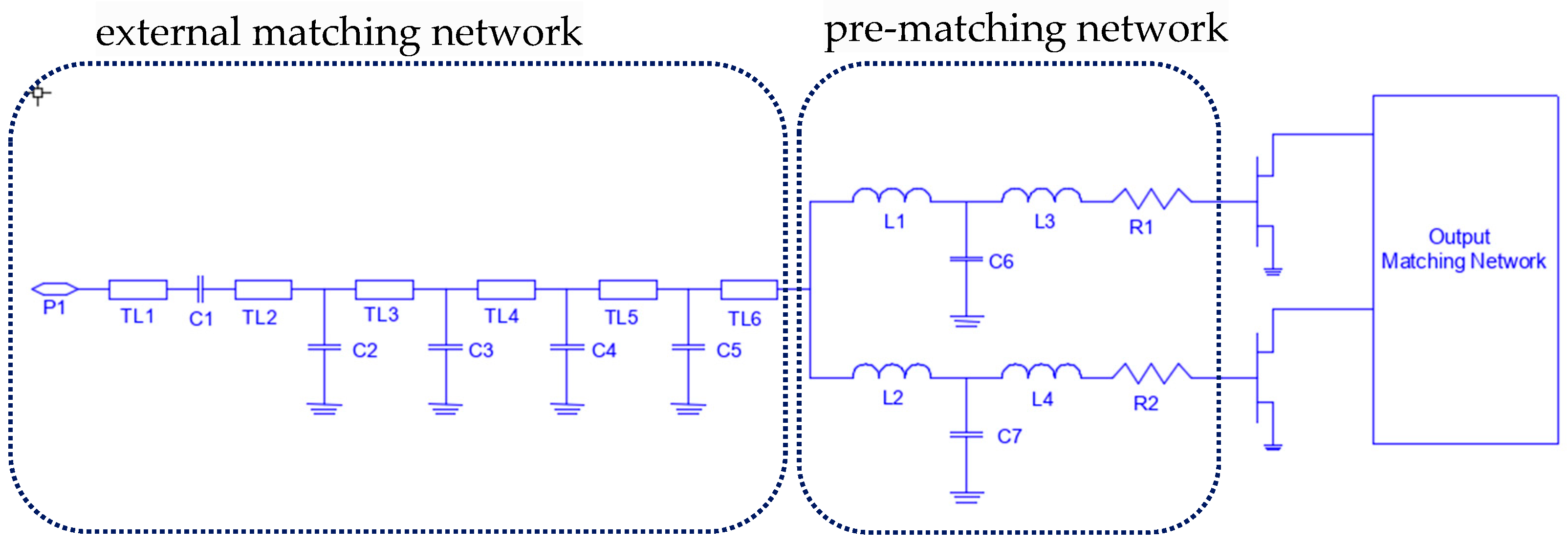
The schematic diagram of the input-matching circuit is shown in Figure 2. The circuit comprises two sections: a pre-matching network and an external matching network. The pre-matching network includes a T-type impedance-matching network and a stability-enhancement network, which, respectively, achieve impedance transformation and stability improvement.
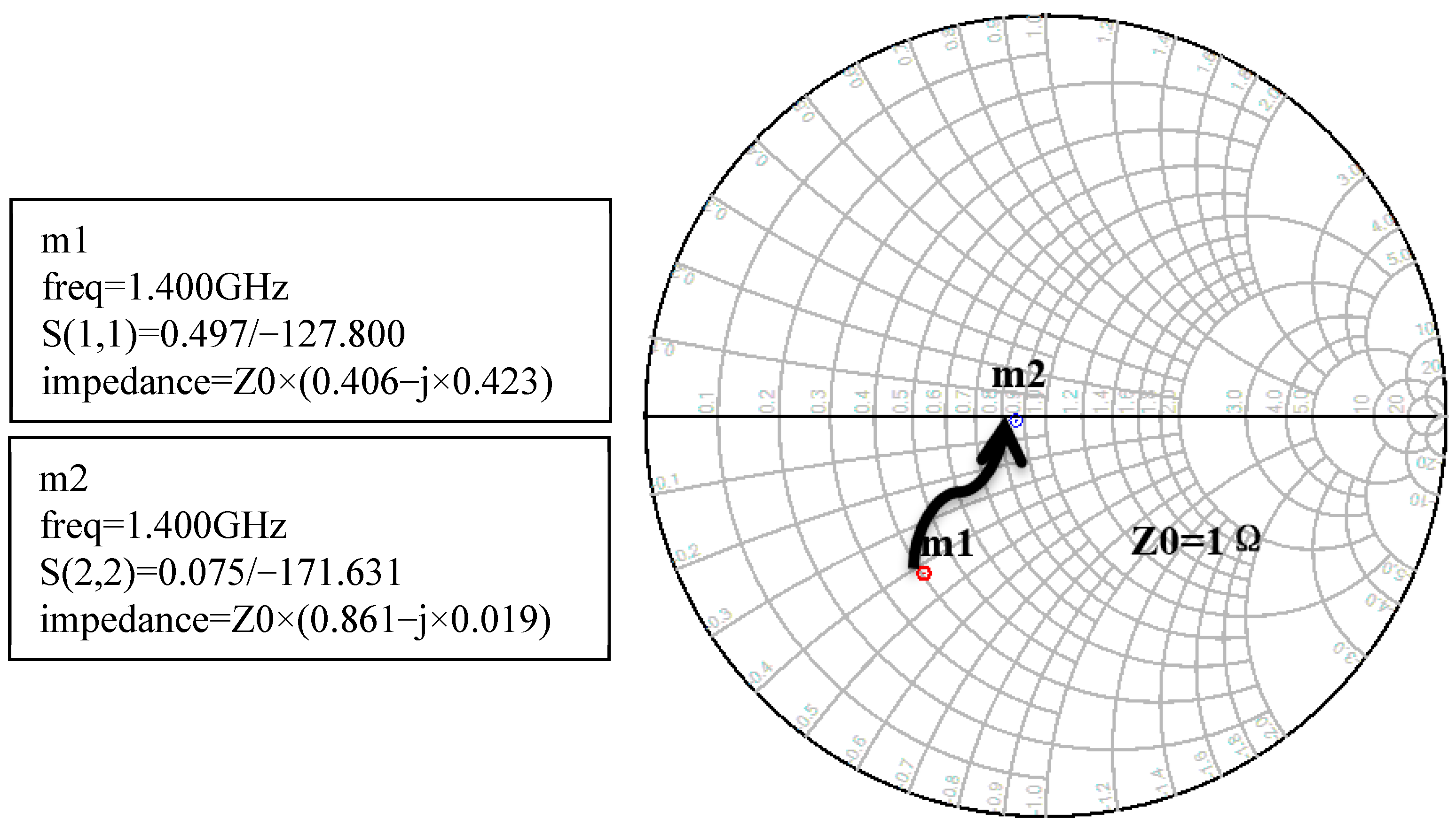
Figure 3 illustrates the input impedance (m1: 0.406 − j × 0.423 Ω) (The input impedance settings of the device are configured as follows: Vds is 50 V, Vgs is −2.8 V, Pin is 10 W, frequency is 1.28 GHz) obtained from large-signal source-pull simulations at a specific frequency point within the L-band. After transformation by the input pre-matching network, the impedance magnitude is approximately doubled, achieving 0.861 − j × 0.019 Ω (m2).
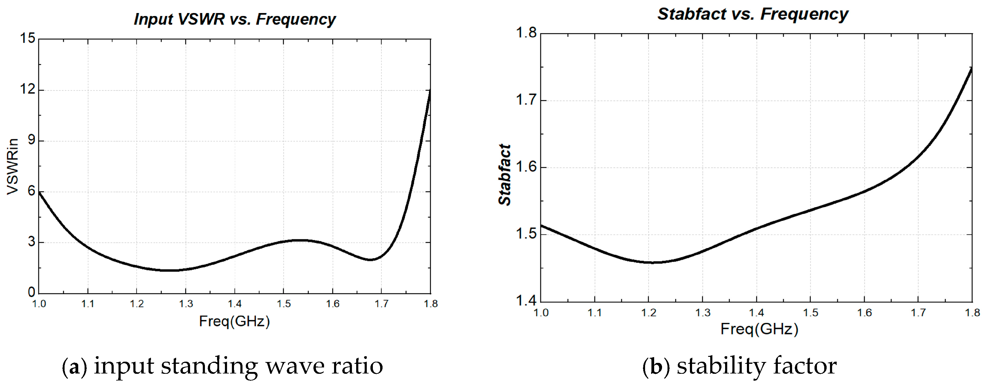
The external input-matching circuit employs a multi-stage hybrid network composed of microstrip capacitors to achieve broadband impedance transformation, enabling the uplifting of the pre-matched impedance to 50 Ω while maintaining a compact circuit size. Figure 4a illustrates the input standing wave simulation results, demonstrating that the input standing wave ratio remains below 3 across the L-band operating frequency range. Figure 4b shows the stability factor simulation results, confirming that the stability factor exceeds one after stability enhancement, ensuring absolute stability, the low-frequency instability is prone to occur in devices with high gain. To assess the out-of-band stability performance, simulations were conducted on the stability factor outside the 0.1–0.8 GHz band. The stability factor within this band exceeds 1.4, indicating excellent stability. To miniaturize the circuit size, the external matching network utilizes high-permittivity PCB substrates for implementation.

2.3. Output-Matching Circuit Design

In continuous conduction mode, the impedance design space is enhanced by introducing a reactance term ( 1 γ s i n ( θ ) ) into the drain voltage formulation while maintaining the real-axis component of the optimal impedance Ropt. This modification broadens the design flexibility without compromising efficiency or output power characteristics. The drain voltage expression under this condition can be expressed as:
V d θ = 1 2 3 cos θ + 1 3 3 cos 3 θ 1 γ sin θ , 1 < γ < 1
The drain current expression is
I d θ = 1 π + 1 2 cos θ + 2 3 π cos 2 θ 4 15 π cos 4 θ +
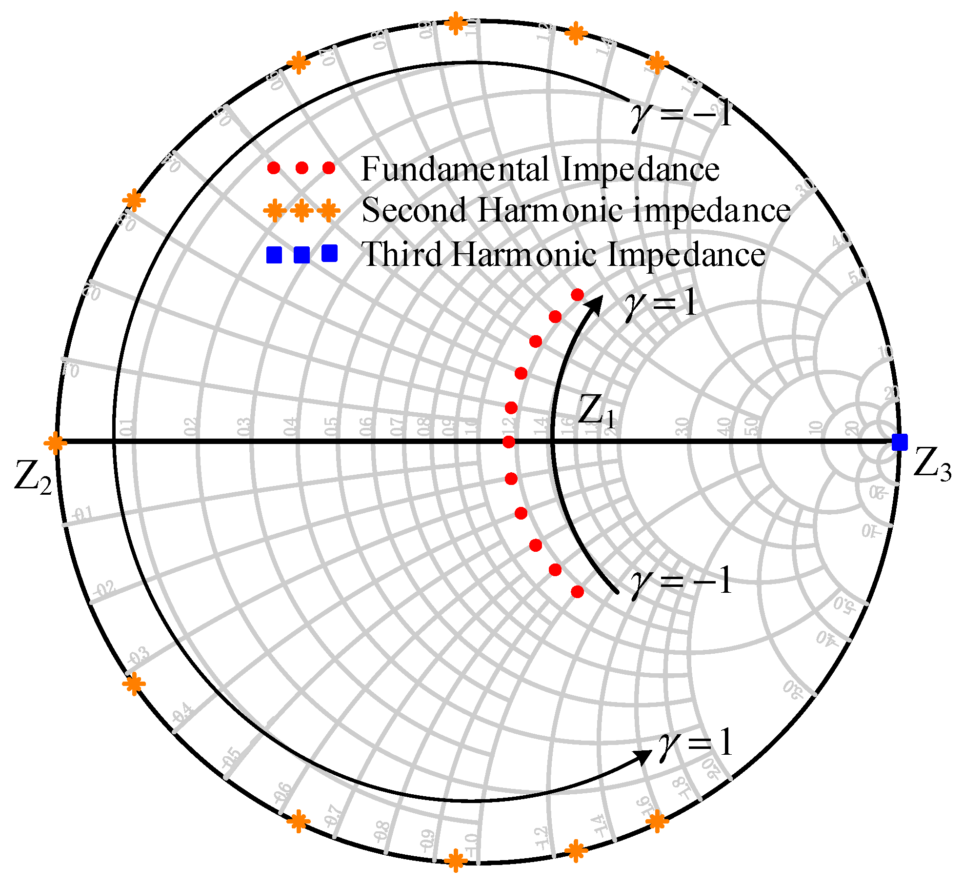
By analyzing the drain voltage and current waveforms, the normalized representations of the optimal fundamental impedance (Z1), second harmonic impedance (Z2), and third harmonic impedance (Z3) can be derived, as depicted in Figure 5, in the figure, the red dot indicates variations in fundamental impedance, the orange dot represents changes in second - harmonic impedance, and the blue dot corresponds to third - harmonic impedance. The normalized impedance magnitude is defined as Ropt.
Z 1 = 2 3 + j γ , 1 < γ < 1
Z 2 = j 7 π 8 3 γ , 1 < γ < 1
Z 3 =
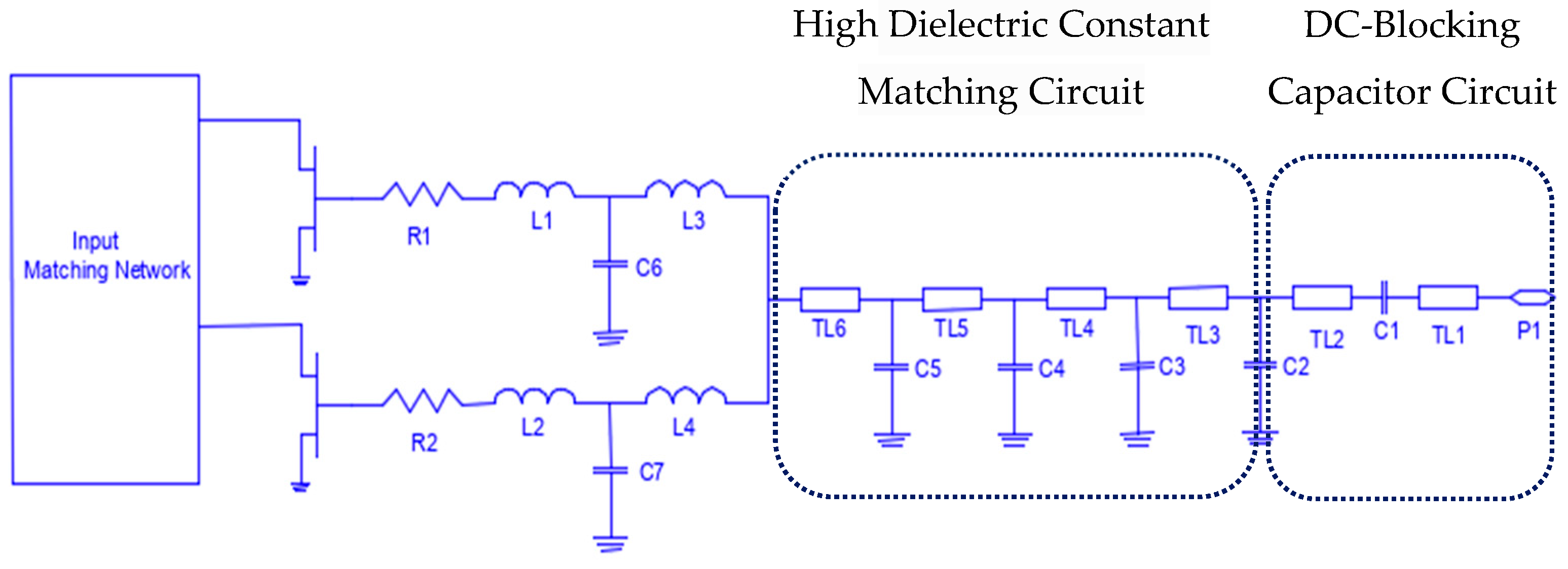
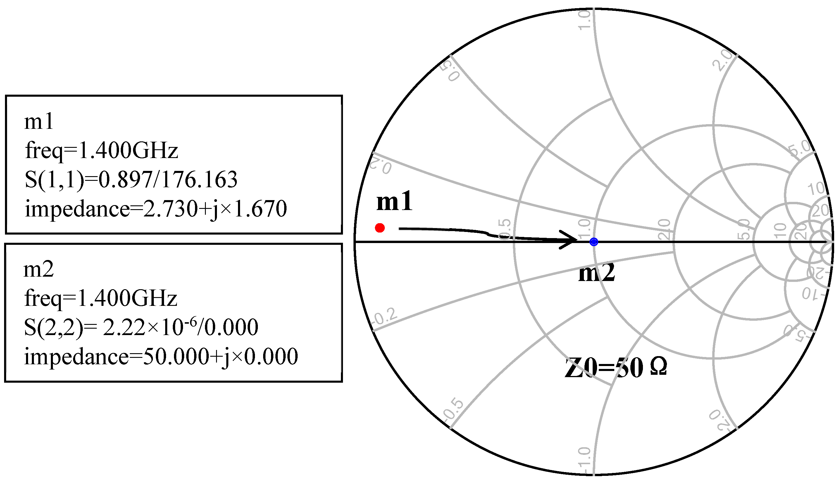
In addition, the designed power amplifier faces challenges including high output power, broad operating bandwidth, and continuous-wave operation. To achieve higher than 400 W output power, the total gate width of the transistor is designed as 72 mm. Load-pull simulations confirm an output load impedance of 2.73 + j × 1.67 Ω (the simulation conditions for output impedance are configured as follows: Vds is 50 V, Vgs is −2.8 V, Pin is 10 W, frequency is 1.4 GHz), requiring an impedance transformation ratio exceeding 18:1 to match the 50 Ω port impedance. This high ratio poses significant challenges in matching network design. The microstrip lines must be wide enough to handle higher than 400 W continuous-wave power, imposing layout constraints due to limited board space and parasitic effects. Under continuous-wave high-power conditions, DC-blocking capacitors are prone to thermal runaway, where localized heating exceeds safe operating limits, severely impacting power amplifier reliability.
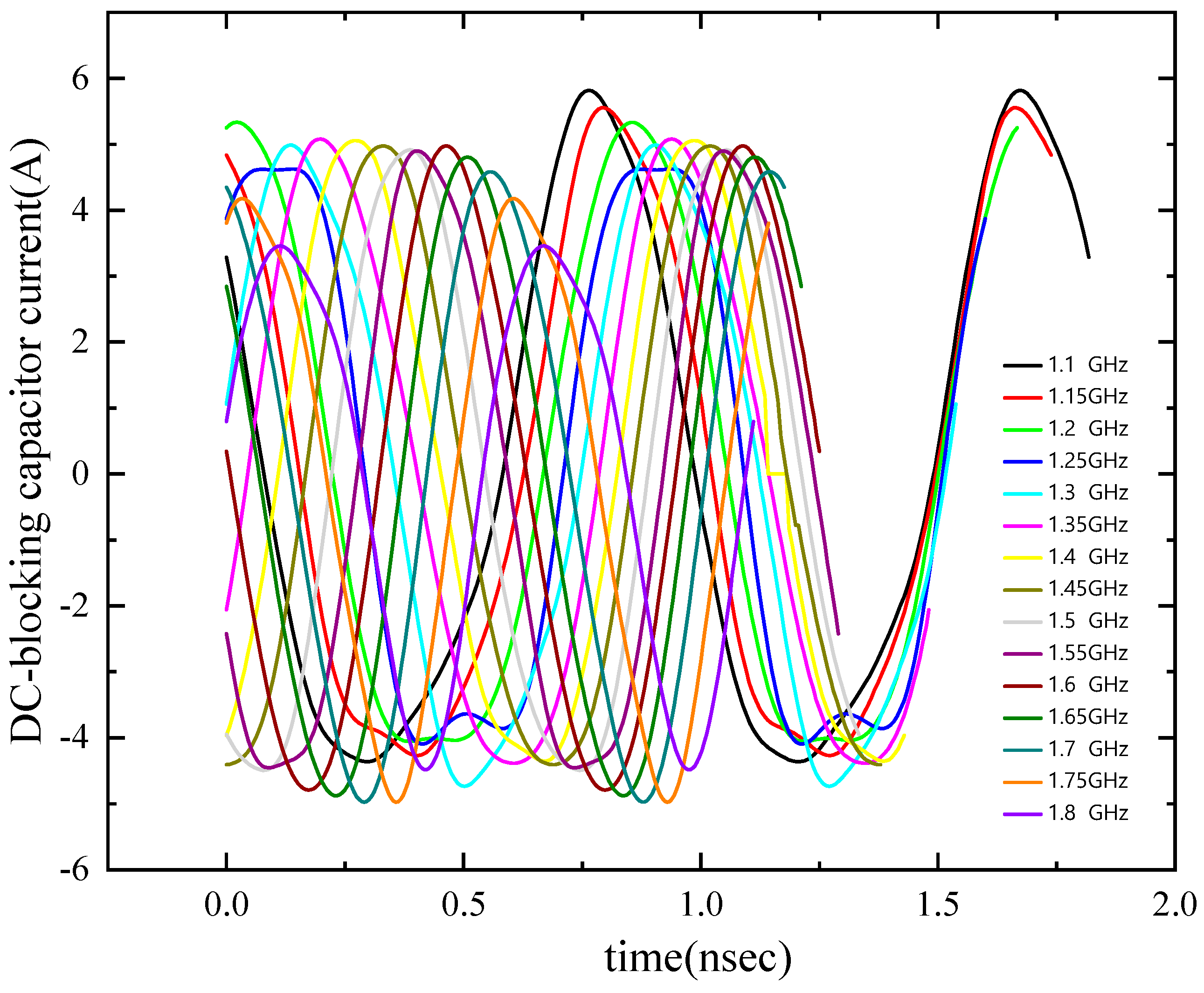
To achieve broadband impedance matching, the output-matching network illustrated in Figure 6 employs eight-section microstrip lines (TL9–TL14 in Figure 6) fabricated on high-permittivity PCB substrates to transform the chip load impedance (2.73 + j × 1.67 Ω, as shown in Figure 7) into a 50 Ω port impedance. To achieve the purpose of minimize temperature rise, we will position the DC-blocking capacitor close to the 50 Ω port, as the high-signal simulation results shown to us, the peak current through the DC-blocking capacitor is 5.5 A (Figure 8 shown us the simulation result),the RMS current is 3.88 A (the simulation conditions for the blocking capacitor’s current waveform are configured as follows: Vds is 50 V, Vgs is −2.8 V, Pin is 10 W, frequency is 1.1~1.8 GHz), the DC-blocking capacitor’s rated current is 6 A, providing substantial reliability margin. In addition, we chose the low ESR and high-Q ceramic capacitors to reduce heating and enhance overpower capability.
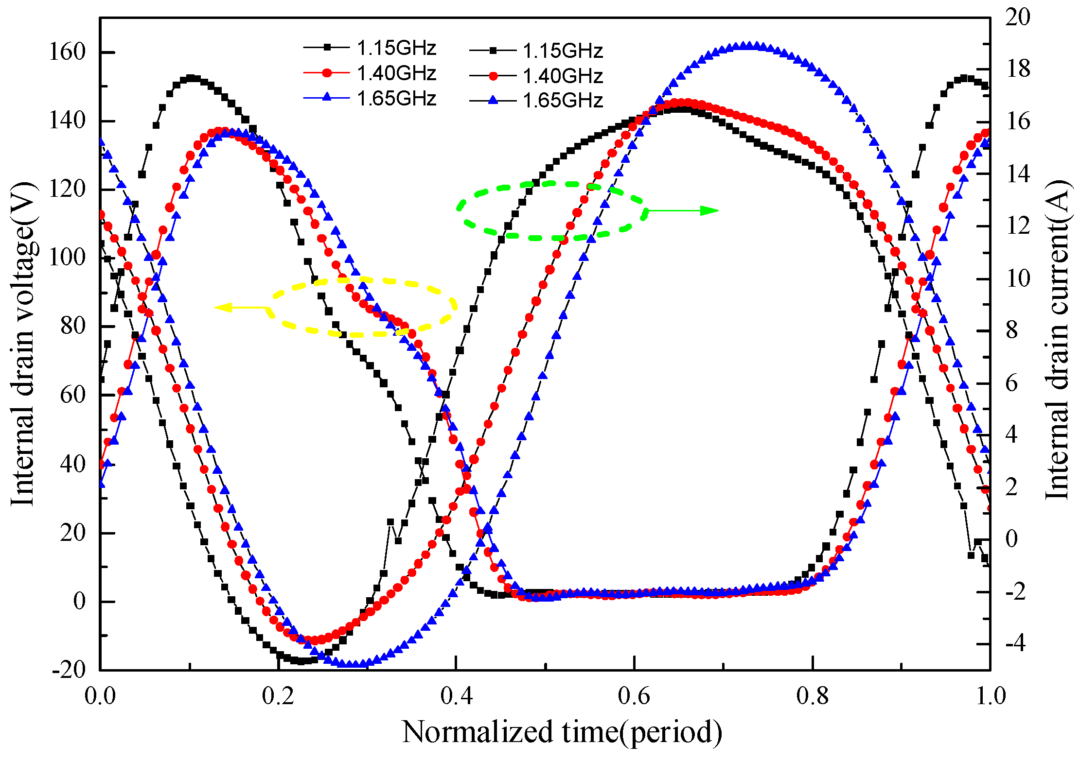
The drain current and voltage characteristics at the device packaging interface were analyzed via simulation results (Figure 9), revealing distinct temporal separation between voltage and current profiles at 1.15, 1.40, and 1.65 GHz, there are two elliptical dashed lines in it, both of which are simultaneously connected to two arrows. Among them, the curve enclosed by the elliptical dashed line connected to the left arrow is the internal drain voltage, and the curve enclosed by the elliptical dashed line connected to the right arrow is the internal drain current. The minimal phase overlap between these waveforms (as depicted in the time domain plots) confirms the amplifier’s operation in a high-efficiency regime, characteristic of continuous mode-switching dynamics.
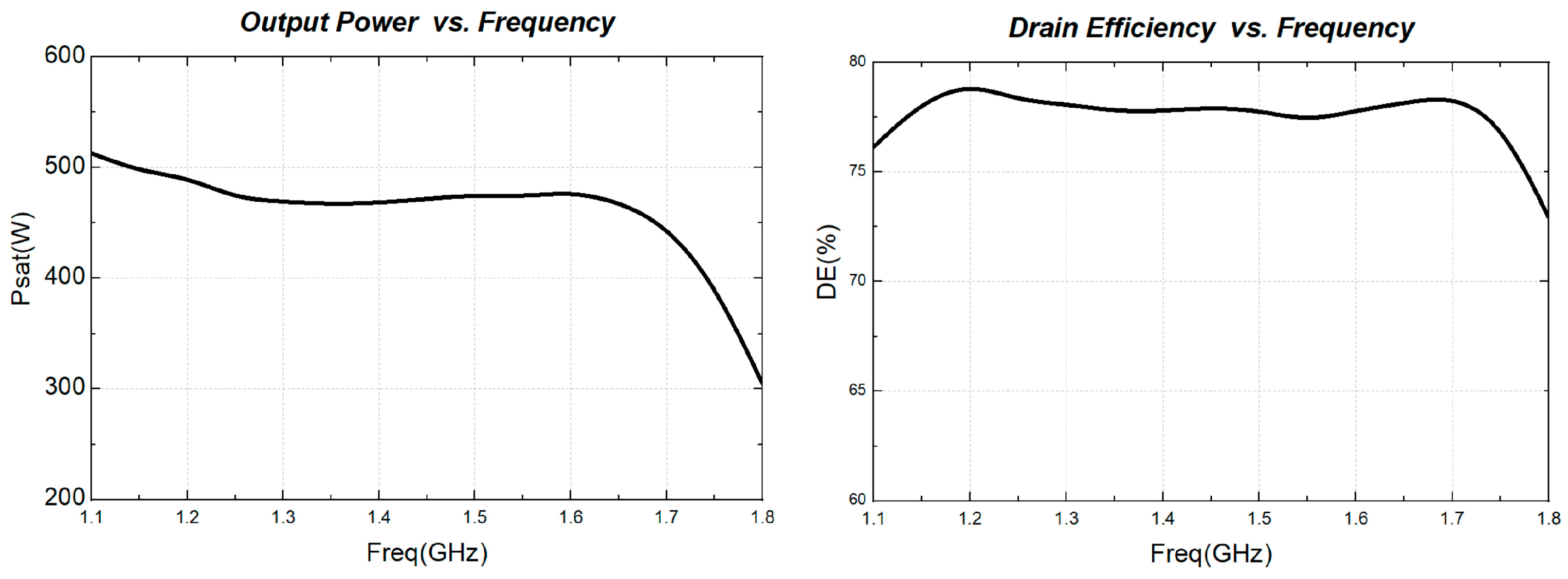
Figure 10 illustrates the simulated output power and drain efficiency of the power amplifier. As shown in the figure, within the L-band under a 50 V operating voltage, the output power exceeds 400 W with a drain efficiency greater than 70%.

2.4. Reliability Design and Evaluation

The power amplifier primarily employs multi-layer ceramic capacitors, GaN chips, and ceramic disc capacitors. The multi-layer ceramic capacitors function as filter capacitors and DC-blocking capacitors, operating under minimal power dissipation with low heat generation and minimal temperature rise. The ceramic disc capacitors are utilized in input matching circuits. Due to the low output power and negligible capacitor losses, The ceramic disc capacitors also exhibit low power dissipation and temperature. In contrast, GaN chips operate at significantly higher temperatures compared to these passive components, making them the hottest elements in the power amplifier. Their thermal performance is critical to the amplifier’s reliability, necessitating lifetime evaluation focused on GaN chips.
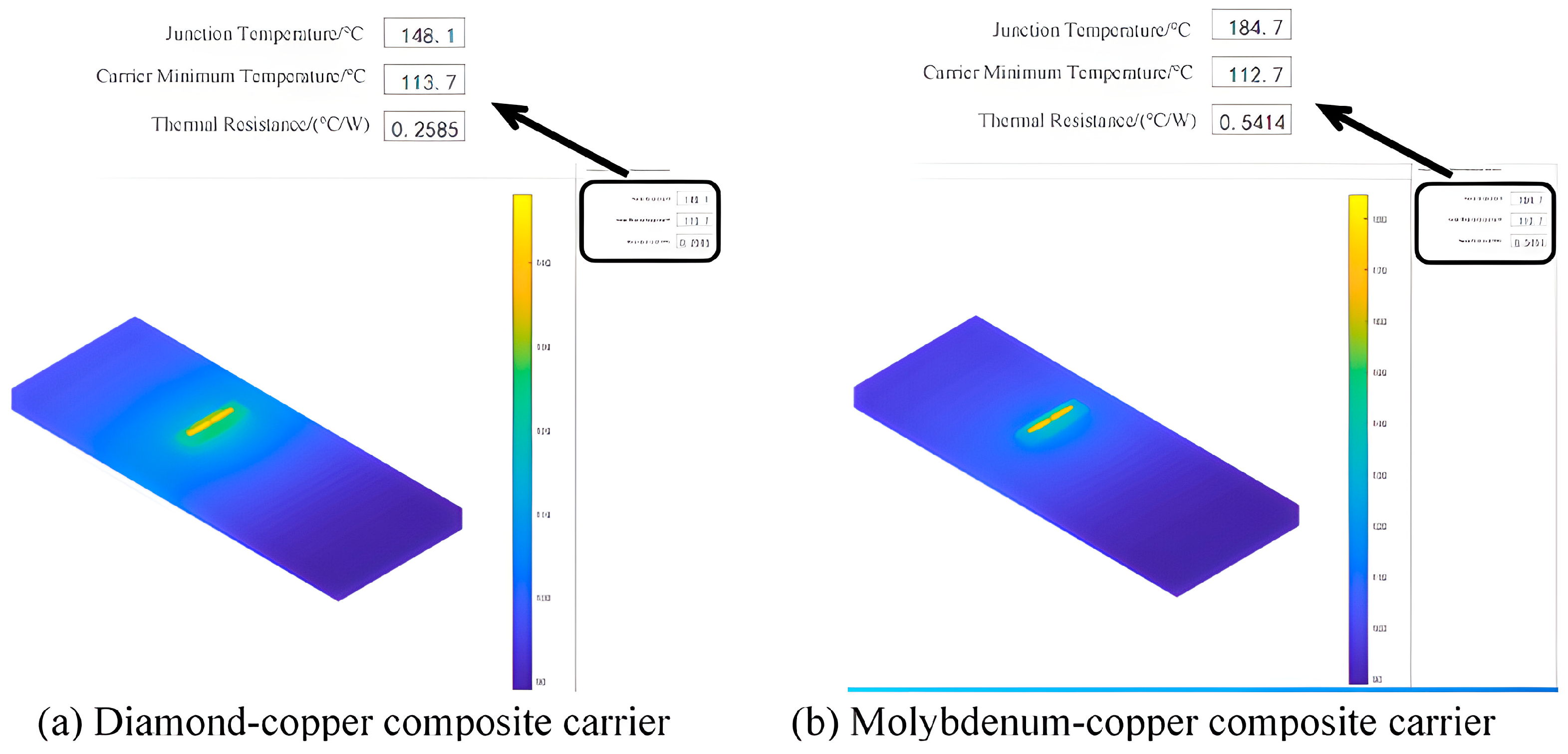
To reduce the operating temperature of the chips, measures such as dual-chip integration, increasing single-chip area, and adopting a diamond–copper composite carrier [8] have significantly reduced the chip junction temperature. Figure 11 presents the thermal simulation results of the power amplifier under continuous-wave operation with an output power of 400 W and a drain efficiency of 75%, for the thermal simulation of the GaN chip, the model is set up as follows: the substrate material of the GaN chip is SiC with a thickness of 100 μm, and the single chip measures 6.5 mm × 1 mm. Two chips are combined to form the assembly. The GaN chip is sintered to the chip carrier using gold–tin (Au80Sn20) solder to form the chip assembly unit. The chip carrier materials used for comparison are molybdenum–copper and diamond–copper, both with a thickness of 1 mm and dimensions of 15 mm × 2 mm. The chip assembly unit is then soldered to a power amplifier copper baseplate (50 mm × 30 mm × 5 mm) using silver-lead-tin solder. Subfigures (a) and (b) show the simulation results using the diamond–copper composite carrier and molybdenum–copper composite carrier, respectively. As shown in the figure, compared to the molybdenum–copper carrier, the diamond–copper composite carrier reduces the maximum chip junction temperature from 184.7 °C to 148.1 °C, achieving a temperature reduction of 36.6 °C.
For lifetime characteristic evaluation of long-lifespan, high-reliability electronic components, conducting long-term lifetime testing under normal stress conditions requires substantial human, material, and time resources. To expedite reliability assessment, temperature-accelerated lifetime testing methodology is employed. To evaluate the operational lifespan of chips fabricated with 50 V/0.5 μm process technology, a 1000 h accelerated lifetime test was conducted. The test results are as follows: three devices operating at a junction temperature of 225 °C for 1000 h exhibited zero failures. Based on the high-temperature operational duration from accelerated testing, the acceleration factor was calculated to extrapolate the operational lifespan under standard temperature conditions. The detailed results are presented below:
The simulation results in Figure 8 indicated that the operating temperature of the power amplifier chip is 148.1 °C. According to the Arrhenius model, the acceleration factor (τ) is calculated as:
τ = e E A K ( 1 T 1 1 T 2 )
While the EA is activation energy (taken as 2.4 eV for GaN process); K is the Boltzmann constant; T1 is operating absolute temperature; T2 is high-temperature accelerated absolute temperature.
The projected operational lifespan of the power amplifier at an operating temperature of 148.1 °C is approximately:
T 148.1 * = τ × T 225 *
While the T 148.1 * represents the operational lifespan at 148.1 °C, T 225 * denotes the cumulative operational duration of test samples accelerated to 225 °C, the calculation results is: T 225 * = 3 × 10 3 and τ = 27,082 , which is derived from experimental results.
T 148.1 * = 27082 × 3 × 1000 = 8.1 × 10 7
The above calculation results indicate that the projected lifespan of the power amplifier is 8.1 × 10 7 h, which meets the requirements for high reliability and long-term operational stability.
Beyond factors influencing long-term reliability, such as operating temperature, trap effects have a critical impact on the performance and reliability of GaN device chips. Literature [9]. indicates that traps inherent in the GaN chip can lead to phenomena like current collapse and on-resistance degradation, significantly affecting chip reliability. During GaN chip production, the influence of trap effects can be mitigated, and device reliability enhanced, by optimizing surface treatment processes, refining material structures, and employing field plates to smooth the electric field distribution.

3. Fabrication and Test Analysis of Power Amplifiers

3.1. Fabrication of Power Amplifiers

The power amplifier adopts a carrier-based structure, comprising an enclosure, input matching PCB units, output matching PCB units, and core assembly units. The PCB and core assembly units are integrated into the amplifier enclosure via soldering processes. To reduce thermal resistance, the enclosure base is made of purple copper material. The input pre-matching components and GaN chips are sintered onto a diamond–copper carrier to form the core assembly unit, which is connected to the PCB via gold bonding wires. Since the device operates in continuous-wave (CW) mode with high output power, simulation results indicate a minimum drain additional efficiency (PAE) of 72%. For a 400 W output power, thermal dissipation exceeds 150 W, necessitating stringent thermal management requirements. During installation, the chip is assembled using a 280 °C gold–tin sintering process, which ensures robust soldering strength while achieving low interfacial thermal resistance, thereby optimizing heat dissipation from the die.
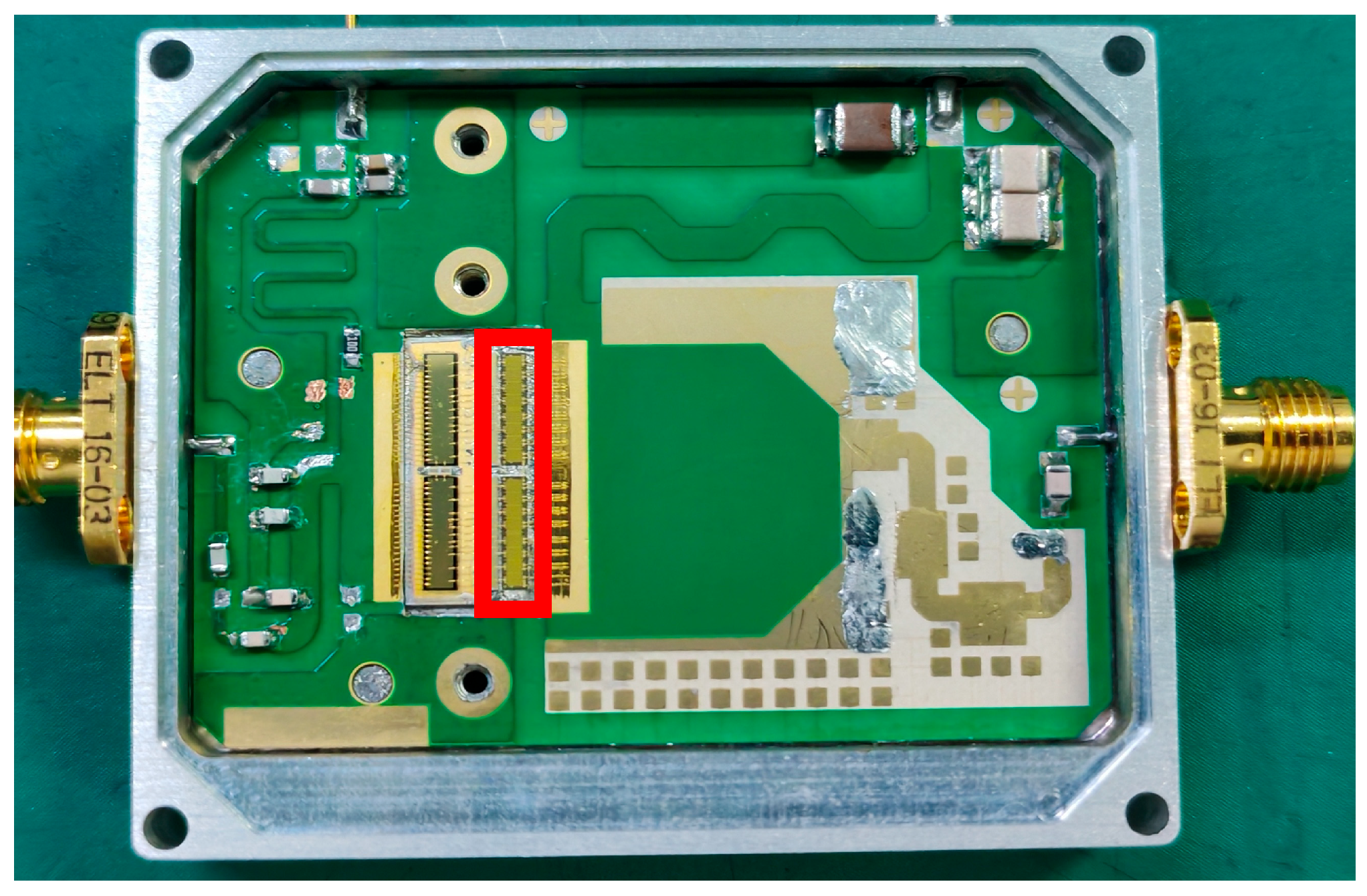
Based on simulation results, the amplifier carrier, input/output matching PCBs, and ceramic capacitors for input pre-matching were designed and fabricated. Post-assembly testing was conducted, with Figure 12 showing the physical photograph of the L-band power amplifier, the red square in the figure indicates the position of the GaN transistor. Due to commercial confidentiality requirements, its external features have been blurred to protect proprietary information.

3.2. Test Results and Analysis

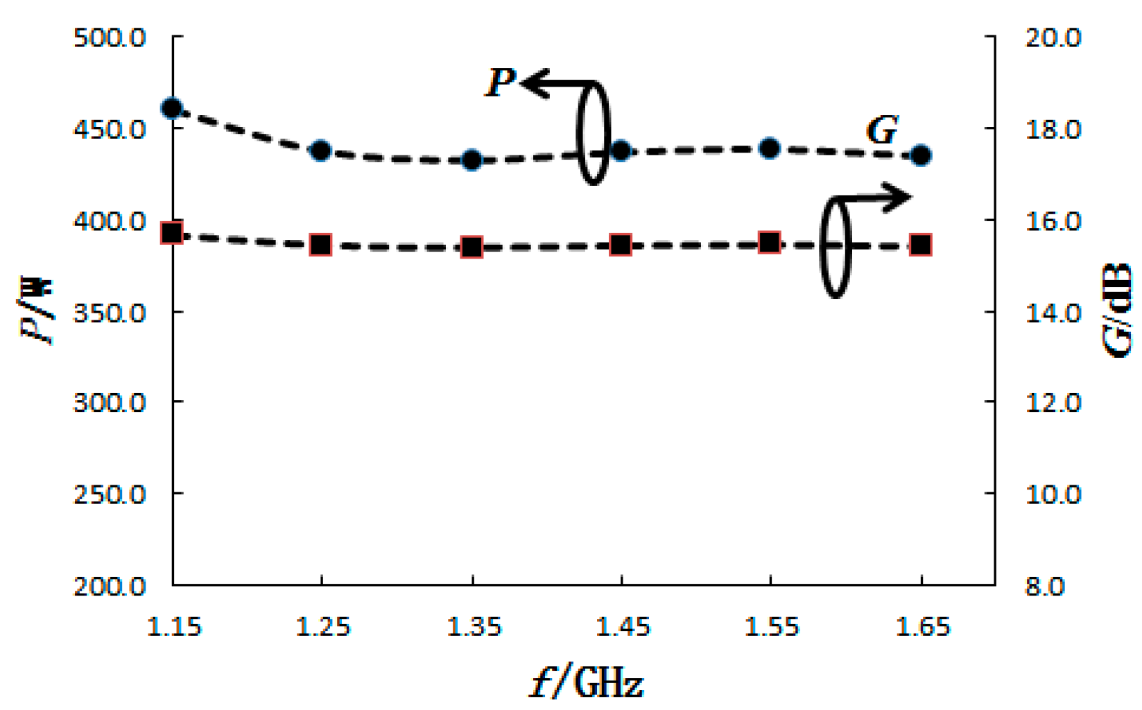
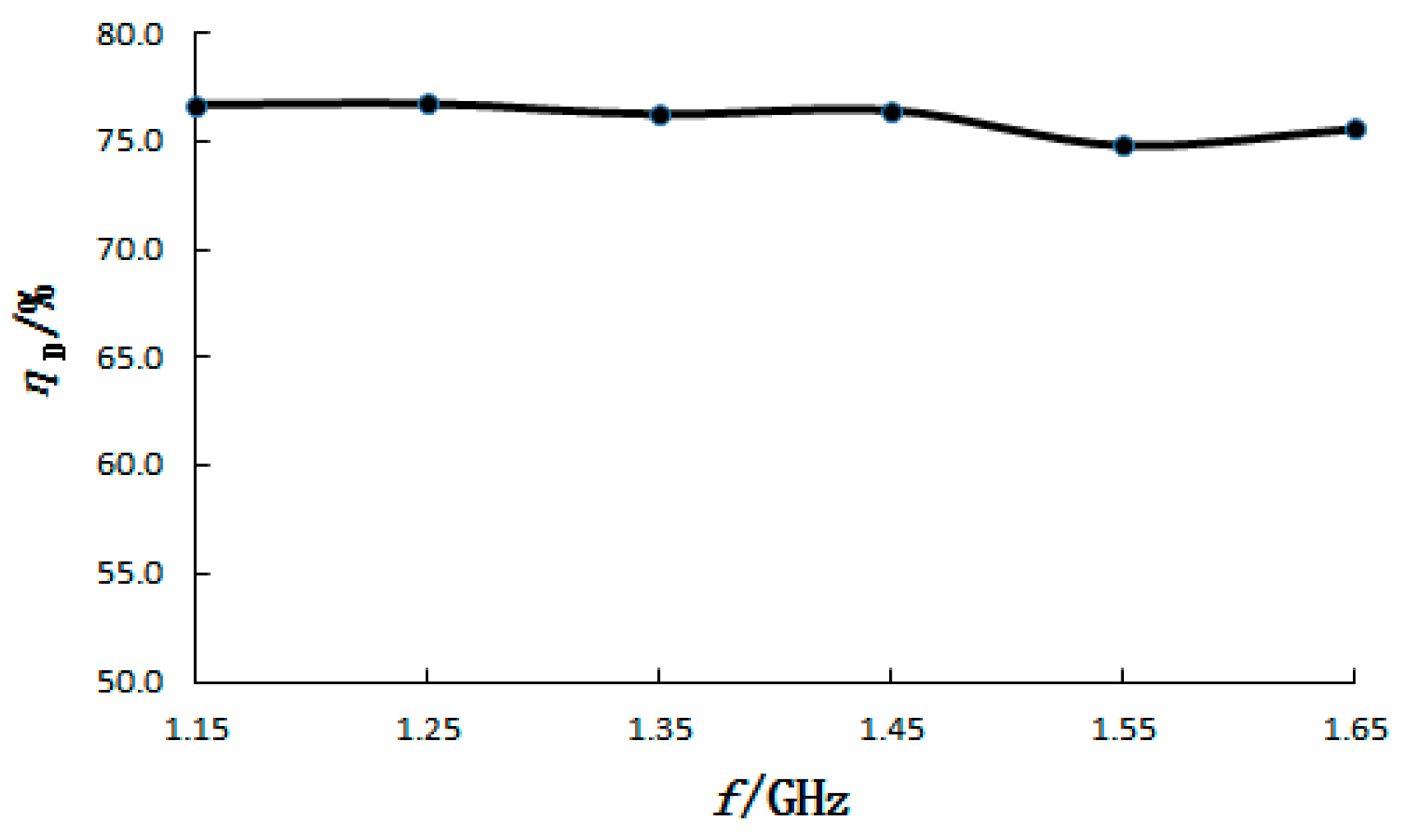
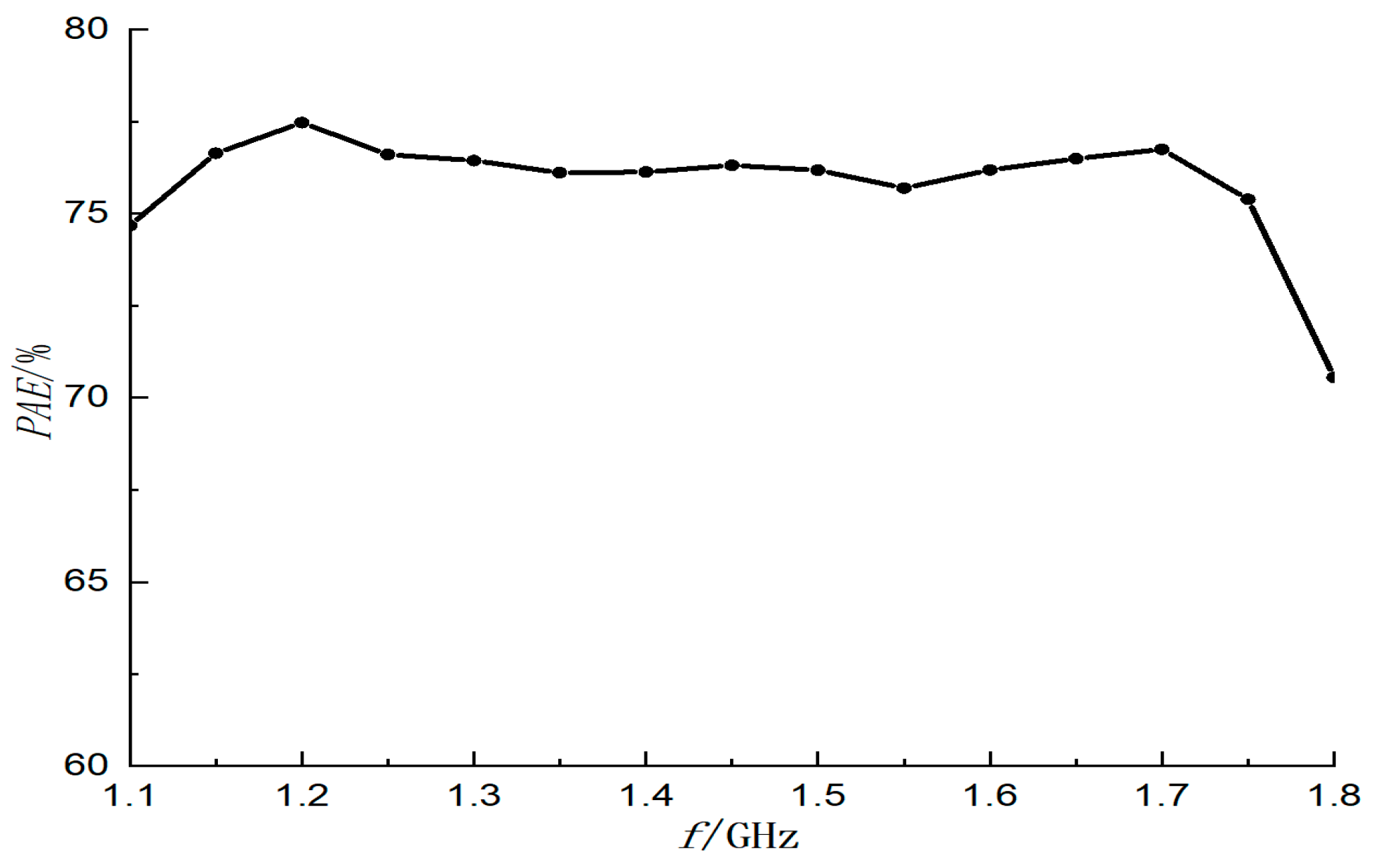
To facilitate testing, the power amplifier is equipped with SMA RF connectors at both input and output ports, enabling direct connection to a high-power microwave test system. The test system comprises: a signal source (providing L-band RF input signals), a driver power amplifier (supplies input drive signals), a DC power supply (providing −2.8 V gate voltage), a high-power DC power supply (delivering 50 V drain voltage), a power analyzer (measuring output signals) and attenuator, isolator, coupler for L-band. The test conditions are as follows: the gate voltage is −2.8 V, the drain voltage is 50 V, the operating mode is continuous-wave (CW), the input power is 41 dBm. To ensure operational safety during testing, high-power heat dissipation devices were employed to maintain adequate thermal management of the power amplifier. The test results are illustrated in Figure 13 and Figure 14. Figure 13 depicts the output power (P) and power gain (G) of the power amplifier as functions of frequency, there are two elliptical solid lines in it, both of which are simultaneously connected to two arrows. Among them, the curve enclosed in the elliptical solid circle connected to the left arrow is the output power(W), and the curve enclosed in the elliptical solid circle connected to the right arrow is the gain(dB). Within the L-band, the minimum output power exceeds 400 W, and the minimum power gain surpasses 15 dB. Figure 14 illustrates the drain efficiency (ηD) of the power amplifier as a function of frequency. Within the L-band, the minimum drain efficiency exceeds 70%. Figure 15 illustrates the test results of the drain power—added efficiency for the power amplifier are presented. According to the test results, the drain power—added efficiency is basically above 70%, similar to the drain efficiency data.
Using an infrared thermal imager for testing, the maximum junction temperature of the chip reaches 152 °C under a 70 °C platform operating temperature when employing a diamond–copper composite carrier. This experimental result aligns well with simulation outcomes, confirming the thermal performance predictability of the diamond/copper heat spreader.
A comparison between measured data and simulation results reveals that the measured data slightly underperforms the simulation outcomes. However, these results still meet the design specifications of the power amplifier presented in this study. The discrepancy primarily stems from idealized assumptions in simulations versus practical manufacturing limitations. Specifically: simulation idealization, simulations assume perfect material properties, geometric symmetry, and absence of parasitic effects, which do not fully account for real-world deviations; die fabrication variability, variations in semiconductor die manufacturing introduce losses not captured in idealized models; assembly challenges, imperfections during power amplifier assembly, such as bonding wire inductance variations and substrate warpage, degrade performance compared to simulated benchmarks. Despite these minor discrepancies, the power amplifier’s critical performance metrics remain within acceptable tolerances for practical deployment.
Table 1 provides a comparative analysis of key performance metrics among various published broadband amplifier designs. The presented architecture demonstrates superior output power, enhanced power-added efficiency (PAD), and an extended operational bandwidth compared to existing solutions.

4. Conclusions

The L-band 400 W continuous-wave GaN power amplifier developed in this study have wide operating bandwidth, high output power, and high efficiency advantages, comparative analysis with existing L-band power amplifier in Table 1 shows the highlights of superior power and efficiency metrics of this work. Meanwhile by implementing measures such as increasing chip area, dual-chip integration, and adopting a diamond–copper carrier, the thermal resistance of the power amplifier is significantly reduced. This enables lower junction temperatures for GaN chips under high-power CW operation. Lifetime estimation results indicate that the power amplifier achieves an MTTF of 8.1 × 10 7 h, meeting the requirements for high reliability and long service life in communication platforms and other applications.

Author Contributions

Conceptualization, X.J. and F.Y.; methodology, X.J. and X.Z.; validation, X.J., X.Z. and K.M.; formal analysis, X.J.; investigation, X.J.; resources, X.J. and X.Z.; data curation, X.J., X.Z. and K.M.; writing—original draft preparation, X.J.; writing—review and editing, K.M.; visualization, K.M.; supervision, F.Y. and H.W.; project administration, X.J.; funding acquisition, X.J. All authors have read and agreed to the published version of the manuscript.

Funding

This research received no external funding.

Data Availability Statement

The original contributions presented in this study are included in the article. Further inquiries can be directed to the corresponding author.

Conflicts of Interest

Author Xiaofan Zhang was employed by the company the 13th Institute of China Electronics Technology Group Corporation. The remaining authors declare that the research was conducted in the absence of any commercial or financial relationships that could be construed as a potential conflict of interest.

References

  1. Jing, X.-D.; Zhong, S.-C.; Wang, H.-L.; You, F. A 150-W Spaceborne GaN Solid-State Power Amplifier for BeiDou Navigation Satellite System. Int. IEEE Trans. Aerosp. Electron. Syst. 2022, 58, 2383–2393. [Google Scholar] [CrossRef]
  2. Andersson, C.M.; Gustafsson, D.; Cahuana, J.C.; Hellberg, R.; Fager, C. A 1–3-GHz digitally controlled dual-RF input power-amplifier design based on a Doherty-outphasing continuum analysis. IEEE Trans. Microw. Theory Tech. 2013, 61, 3743–3752. [Google Scholar] [CrossRef]
  3. Ruiz, M.N.; Benito, A.L.; Pérez-Cisneros, J.R.; Gilabert, P.L.; Montoro, G.; García, J.A. Constant-gain envelope tracking in a UHF outphasing transmitter based on continuous-mode class-E GaN HEMT PAs. In Proceedings of the 2016 IEEE MTT-S International Microwave Symposium (IMS), San Francisco, CA, USA, 22–27 May 2016; IEEE: New York, NY, USA, 2016; pp. 1–4. [Google Scholar]
  4. Giofré, R.; Colantonio, P.; González, L.; De Arriba, F.; Cabrìa, L.; Molina, D.L.; Garrido, E.C.; Vitobello, F. Design realization and tests of a space-borne gan solid state power amplifier for second generation Galileo navigation system. IEEE Trans. Aerosp. Electron. Syst. 2018, 54, 2383–2396. [Google Scholar] [CrossRef]
  5. Maassen, D.; Boet, J.D.; Zanden, J.V.D.; Heeres, R.M.; Rijs, F.V. Comparison between latest Si-LDMOS and GaN technology for RF-Power base station transistors. In Proceedings of the 2023 53rd European Microwave Conference (EuMC), Berlin, Germany, 19–21 September 2023; pp. 283–286. [Google Scholar] [CrossRef]
  6. Nuttinck, S.; Gebara, E.; Laskar, J.; Rorsman, N.; Olsson, J.; Zirath, H.; Eklund, K.; Harris, M. Comparison between Si-LDMOS and GaN-based microwave power transistors. In Proceedings of the IEEE Lester Eastman Conference on High Performance Devices, Newark, DE, USA, 8 August 2002; pp. 149–154. [Google Scholar]
  7. Wang, Y.; Cao, L. Status in U.S. AESA fighter radar and development trends. In Proceedings of the IET International Radar Conference 2013, Xi’an, China, 14–16 April 2013; pp. 1–6. [Google Scholar]
  8. Jiayu, L.; Su, P.; Yu, Z.; Zhang, H.; Peng, Y.; Chen, M. Near-junction heat dissipation of high-power chips by copper-diamond based heat sink. In Proceedings of the 2025 26th International Conference on Electronic Packaging Technology (ICEPT), Shanghai, China, 5–7 August 2025; pp. 1–3. [Google Scholar]
  9. Gibiino, G.P.; Nunes, L.C.; Miller, N.C. Advancing RF GaN HEMTs: A Perspective on Measurement and Characterization Techniques. IEEE Microw. Mag. 2025, 26, 18–31. [Google Scholar] [CrossRef]
  10. Rochette, S.; Vendier, O.; Langrez, D.; Cazaux, J.L.; Kuball, M.; Buchta, M.; Xiong, A. A high efficiency 140W power amplifier based on a single GaN HEMT device for space applications in L-band. In Proceedings of the 2012 7th European Microwave Integrated Circuit Conference, Amsterdam, The Netherlands, 29–30 October 2012; pp. 127–130. [Google Scholar]
  11. Available online: https://www.necspace.co.jp/en/products/payload/sspa.html (accessed on 22 November 2025).
  12. Osawa, K.; Yoshikoshi, H.; Nitta, A.; Tanaka, T.; Mitani, E.; Satoh, T. Over 74% efficiency, L-band 200W GaN-HEMT for space applications. In Proceedings of the 2016 46th European Microwave Conference (EuMC), London, UK, 4–6 October 2016; pp. 397–400. [Google Scholar]
  13. Yang, F.; Yin, K.; Zhao, H.; Zhao, Y.; Liu, J.; Yang, S. High power high efficiency solid state power amplifier used in space. Chin. Space Sci. Technol. 2023, 43, 55–62. [Google Scholar]
  14. Katz, A.; MacDonald, J.; Dorval, R.; Eggleston, B.; Drexler, P.; Liang, C. High-efficiency high-power linearized L-band SSPA for navigational satellites. In Proceedings of the 2017 IEEE MTT-S International Microwave Symposium (IMS), Honololu, HI, USA, 4–9 June 2017; pp. 1834–1837. [Google Scholar]
  15. Shen, X.; Zhang, L.; Dai, J.; Yang, J.; Zhou, B. L-band SSPA for Future Payloads exploiting GaN Technology. In Proceedings of the 2020 International Conference on Microwave and Millimeter Wave Technology (ICMMT), Shanghai, China, 17–20 May 2020; pp. 1–3. [Google Scholar]
  16. Giofre, R.; Cabria, L.; De Arriba, F.; Rapisarda, M.; Cipriani, E.; Colantonio, P. A flexible and efficient GaN-Based SSPA for next-generation L-Band reconfigurable payloads. IEEE Trans. Microw. Theory Tech. 2025, 1–15. [Google Scholar] [CrossRef]
Figure 1. The layout diagram illustrates the single-die configuration.
Electronics 15 00203 g001
Figure 2. Schematic diagram of power amplifier input-matching network.
Electronics 15 00203 g002
Figure 3. Input impedance of the GaN HEMT device and impedance after pre-matching transformation.
Electronics 15 00203 g003
Figure 4. Input standing wave and stability factor simulation results.
Electronics 15 00203 g004
Figure 5. The continuous-mode high-efficiency load impedance space.
Electronics 15 00203 g005
Figure 6. Power amplifier output matching circuit schematic diagram.
Electronics 15 00203 g006
Figure 7. Large-signal load-pull simulation results.
Electronics 15 00203 g007
Figure 8. DC-blocking capacitor current simulation results.
Electronics 15 00203 g008
Figure 9. The simulated voltage and current waveforms of the package plane at 1.15, 1.40, and 1.65 GHz.
Electronics 15 00203 g009
Figure 10. Output power and drain efficiency simulation results.
Electronics 15 00203 g010
Figure 11. Thermal simulation results of GaN PA chips on diamond and molybdenum–copper carriers.
Electronics 15 00203 g011
Figure 12. Photograph of the L-band power amplifier.
Electronics 15 00203 g012
Figure 13. Within in the L-band, the output power (P) and power gain (G) of the power amplifier as functions of frequency.
Electronics 15 00203 g013
Figure 14. Within the L-band, the drain efficiency (ηD) of the power amplifier as a function of frequency.
Electronics 15 00203 g014
Figure 15. Within the L-band, the drain power-added efficiency of the power amplifier as a function of frequency.
Electronics 15 00203 g015
Table 1. Performance comparison to the reported works.
RefFreq (GHz)PAD (%)Pout (W)
[1]1.15–1.2350150
[4]1.55–1.644300
[10]1.2–1.3260140
[11]1.52–1.565565
[12]1.53–1.6369190
[13]1.45–1.5564200
[14]1.1–1.660400
[15]L–band5020
[16]1.55–1.647300
This work1.1–1.670400
Disclaimer/Publisher’s Note: The statements, opinions and data contained in all publications are solely those of the individual author(s) and contributor(s) and not of MDPI and/or the editor(s). MDPI and/or the editor(s) disclaim responsibility for any injury to people or property resulting from any ideas, methods, instructions or products referred to in the content.