Design and Optimization of LTCC Broadband Interconnect Structures for Bare-Chip Integration
Abstract
1. Introduction
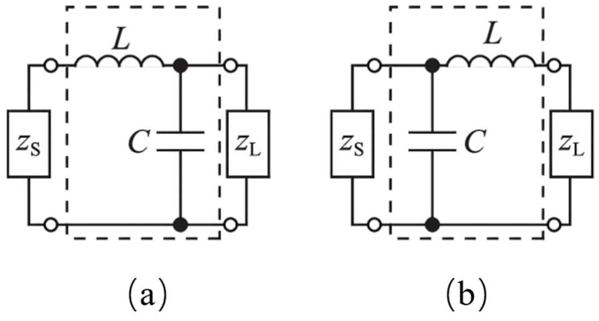
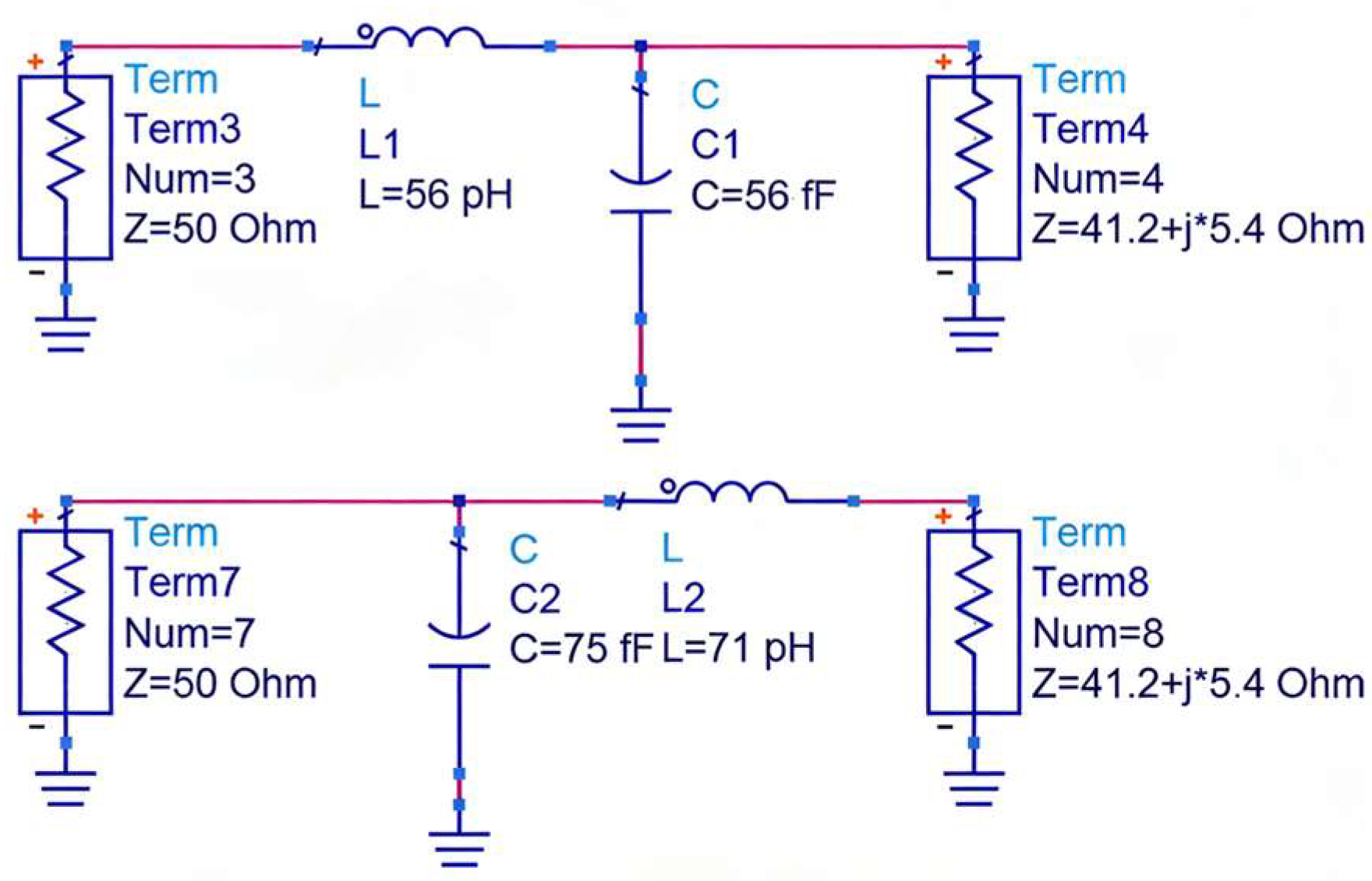
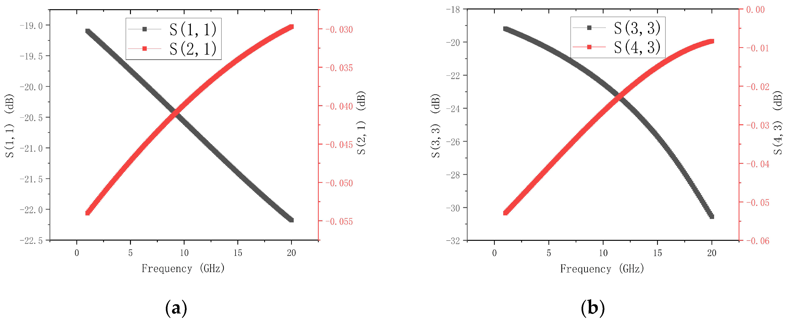
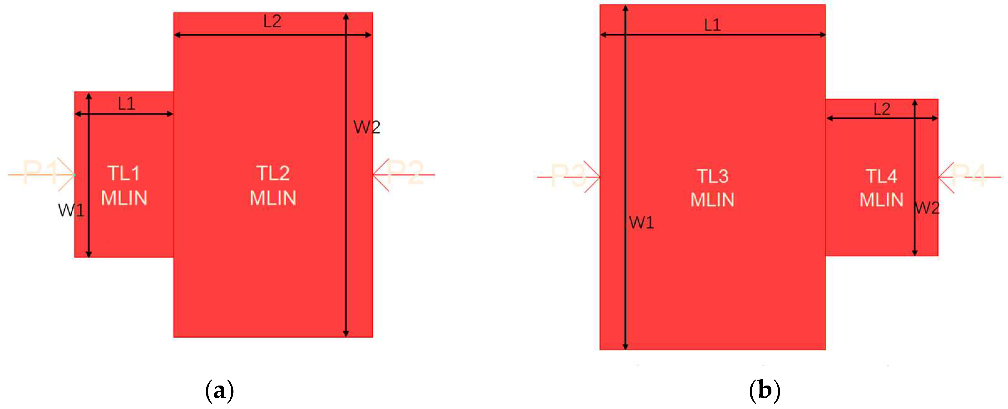
- A T-type microstrip matching network is constructed based on the complex impedance input of a bare chip, and matching is optimized by comparing two matching circuits.
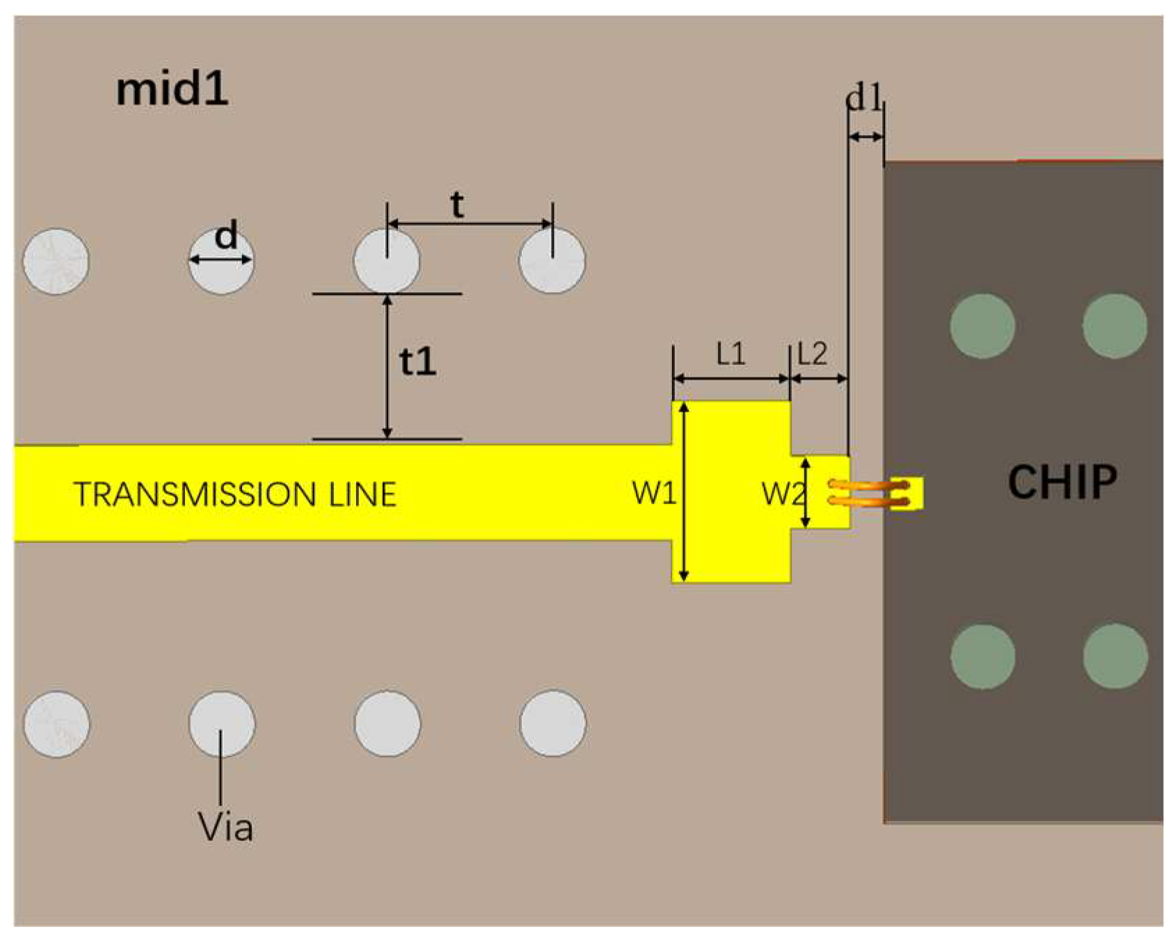
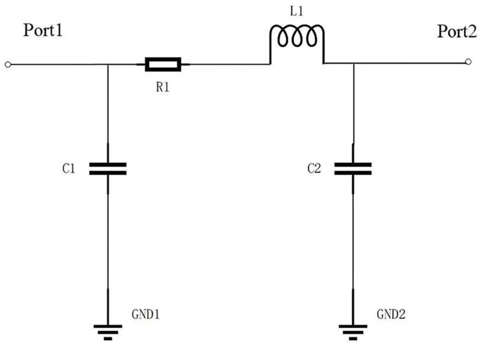
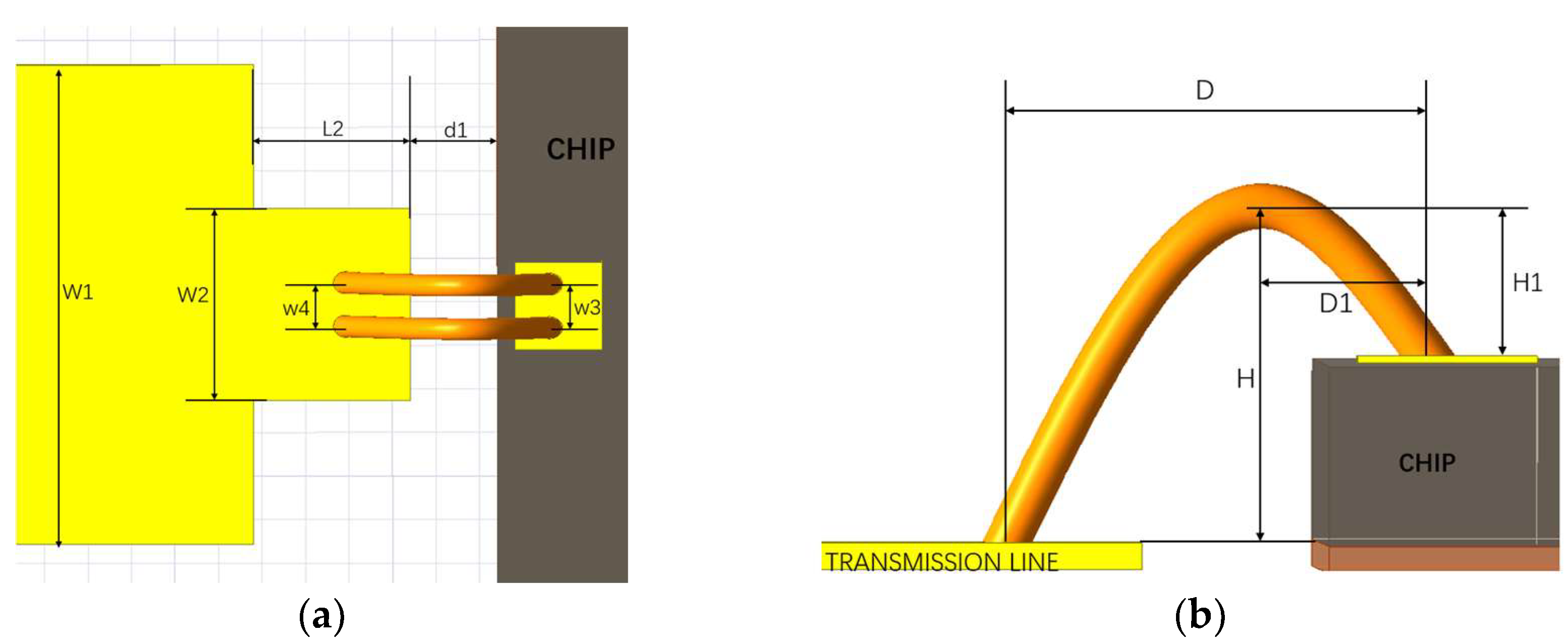
- Bonded Interconnect Layer: Establish a microstrip–gold-wire bond–bare die interconnect model, analyze bonding parasitic mechanisms, and determine the optimal bond center spacing to suppress parasitic inductance imbalance.
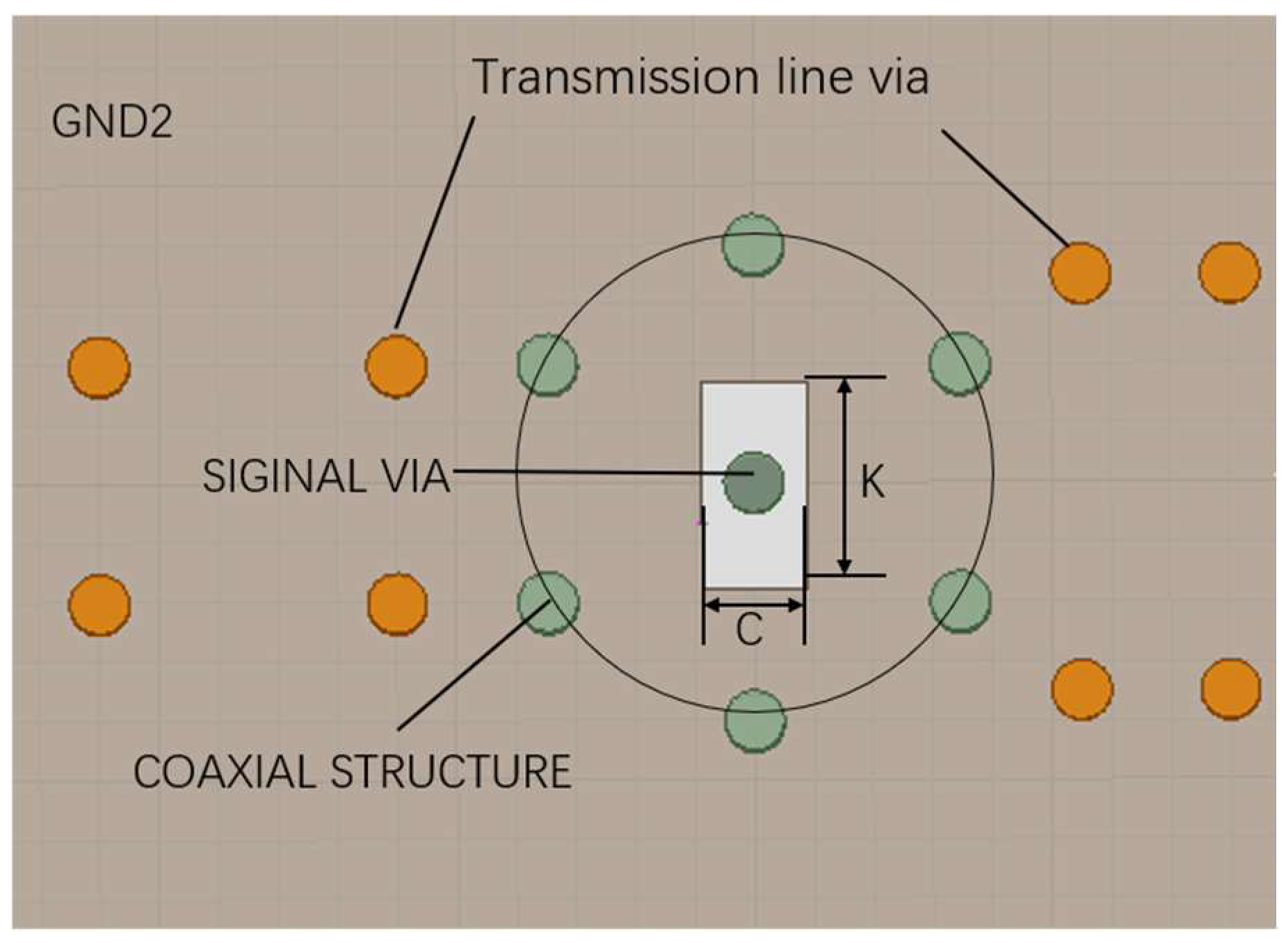
- A coaxial-like via structure combined with a square defected ground structure (DGS) is proposed to enhance impedance continuity and electromagnetic field confinement in stripline–via–microstrip transitions.
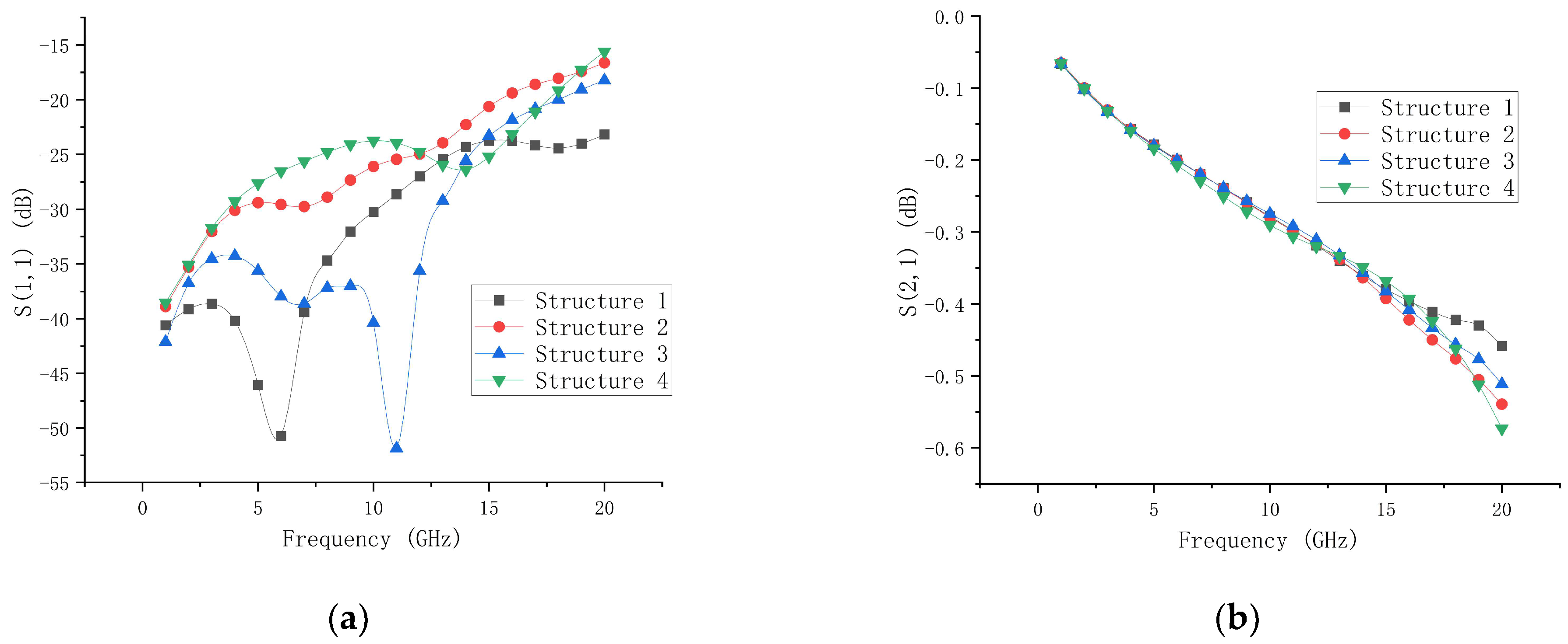
- Full-path verification: Full-wave cascaded simulations in HFSS are performed to validate the broadband performance of the proposed interconnect architecture. The designed interconnect structure achieves S11 < −23.1 dB and S21 < 0.45 dB across the 1–20 GHz frequency range, demonstrating significant advantages over conventional structures.
2. Proposed Methods
2.1. Matching Network Design
2.2. Coaxial-like Structure
2.3. Defect Ground Structure
3. Simulation Study
3.1. T-Type Matching Network Design
3.2. Optimized Design for Microstrip–Gold-Wire Bonding–Bare-Chip Interconnections
3.2.1. Effect of Gold-Wire Bonding Center Spacing on RF Performance
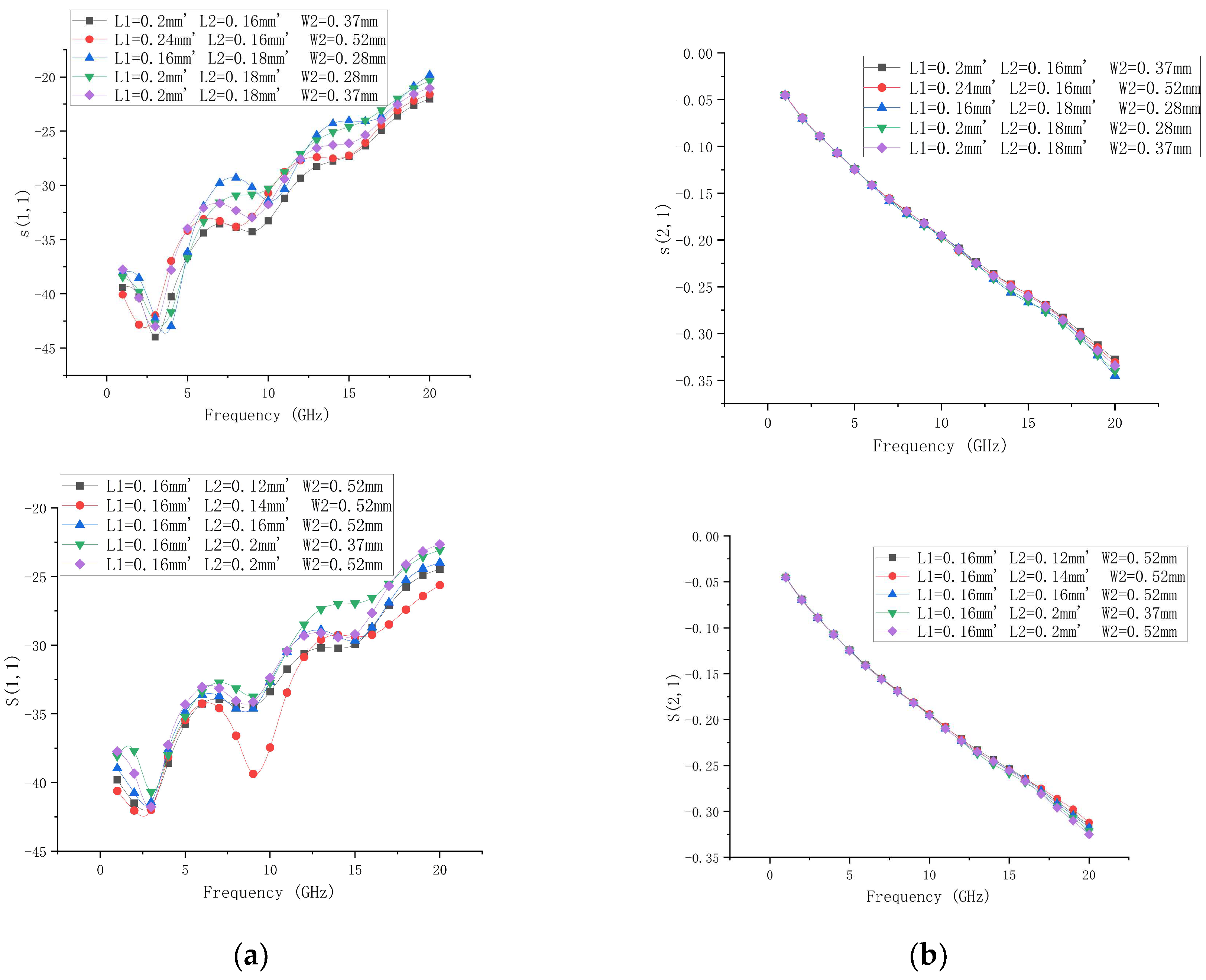
3.2.2. Optimization of T-Type Matching Networks
3.3. Stripline–Microstrip Interlayer Interconnect Structure Design
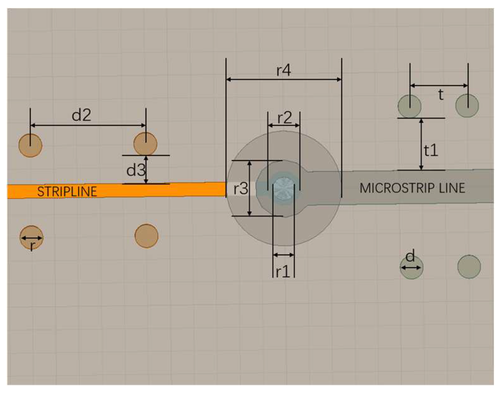
3.3.1. Simulation Design of Via Interconnection Structures
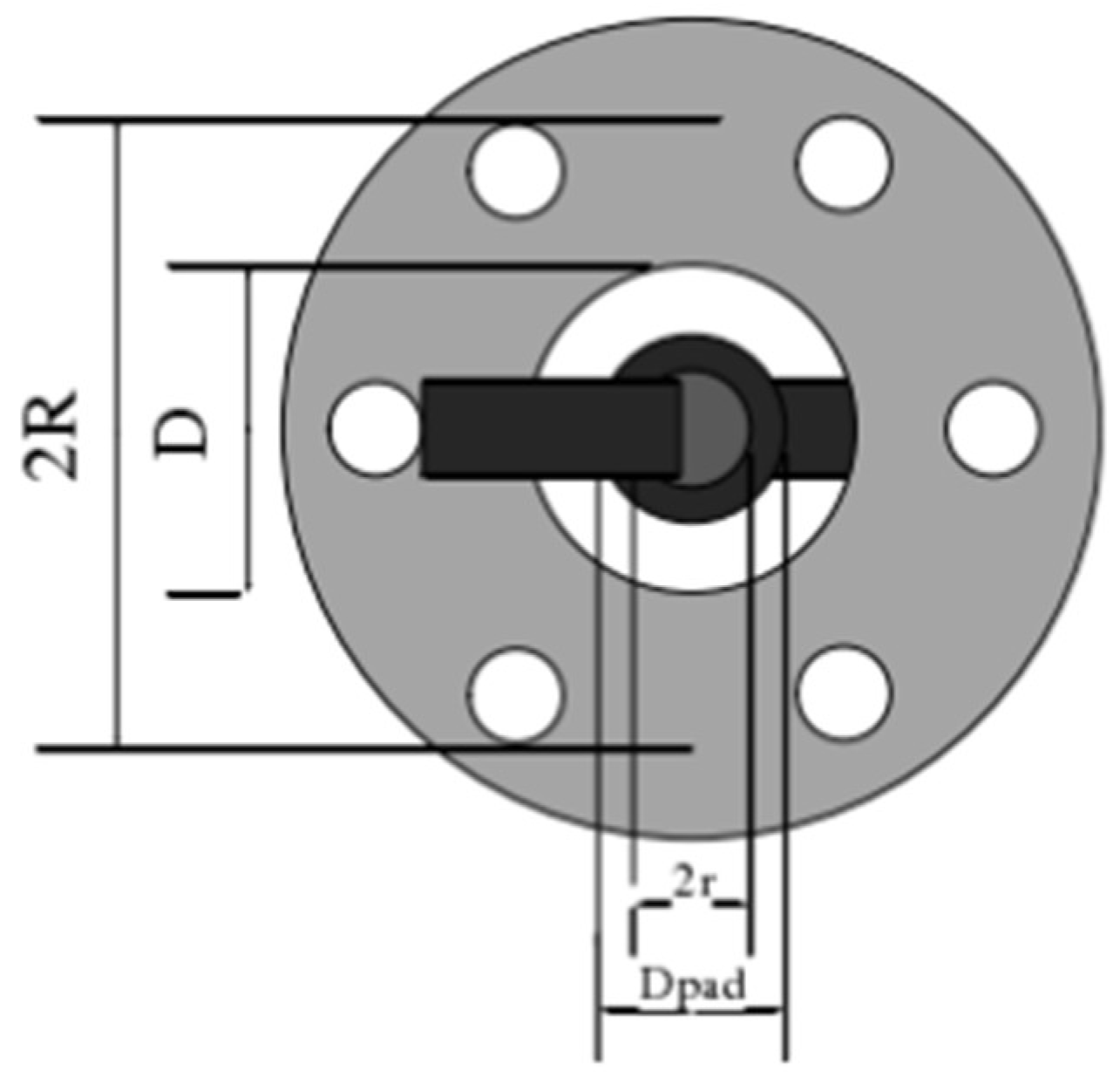
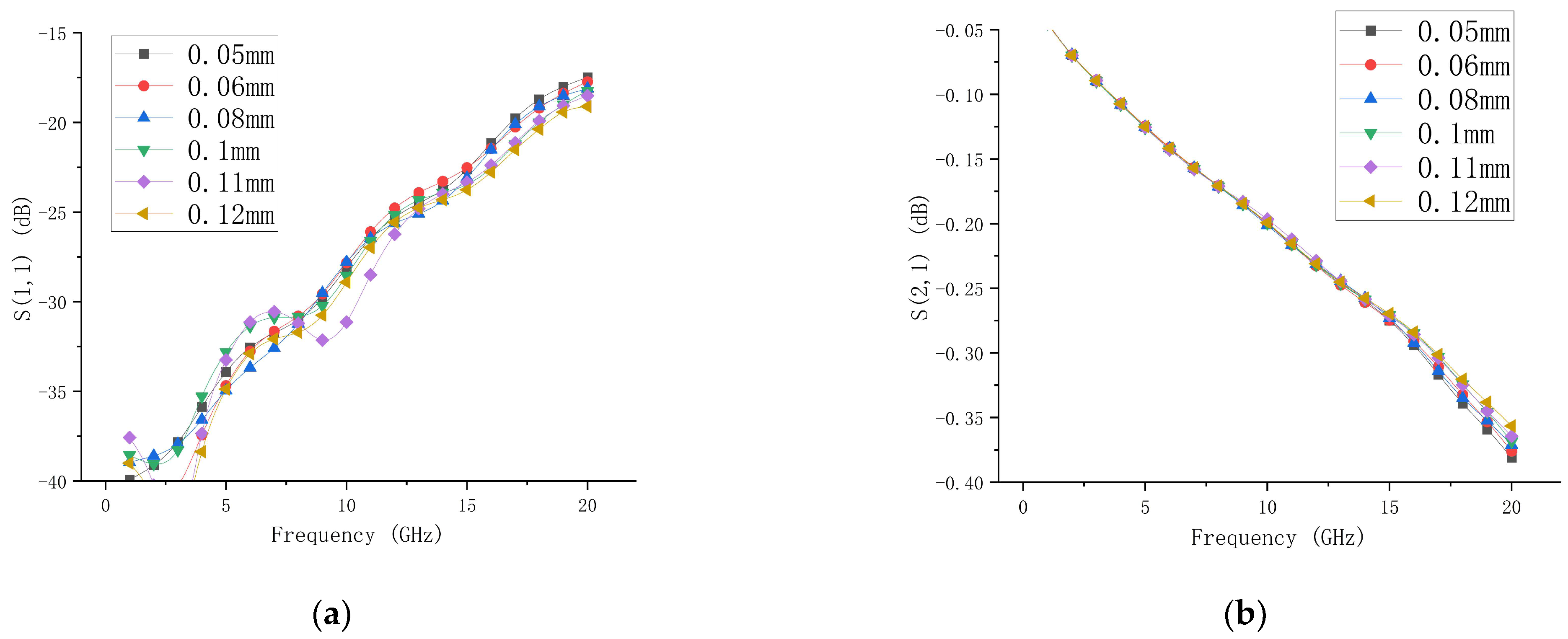
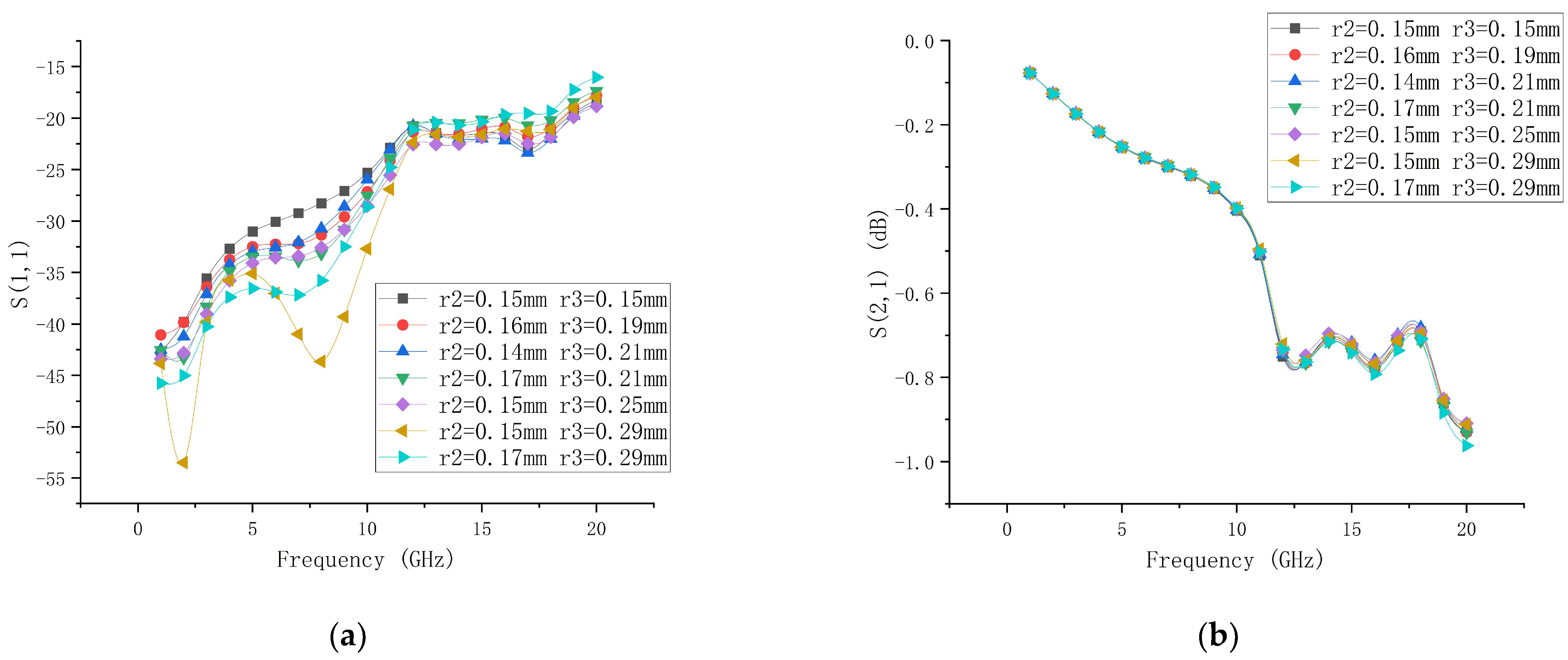
- Effect of Pad Radii r2 and r3 on Transmission Characteristics
- 2.
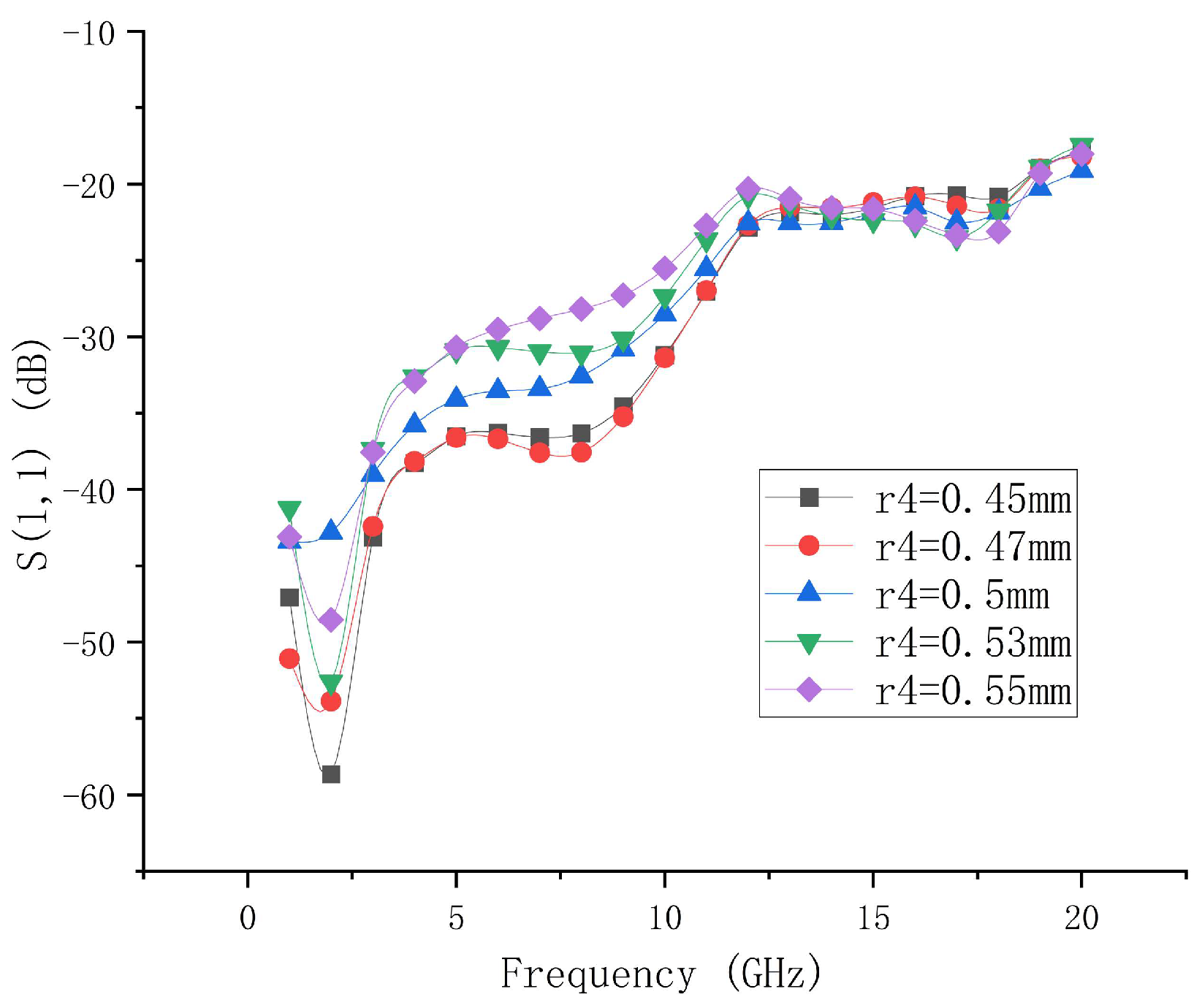
- The Effect of Isolation Disc R4 on Transmission Characteristics
3.3.2. Optimization of Via Interconnection Structures
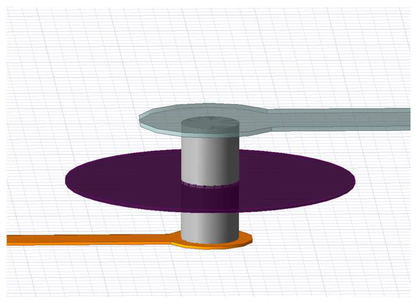
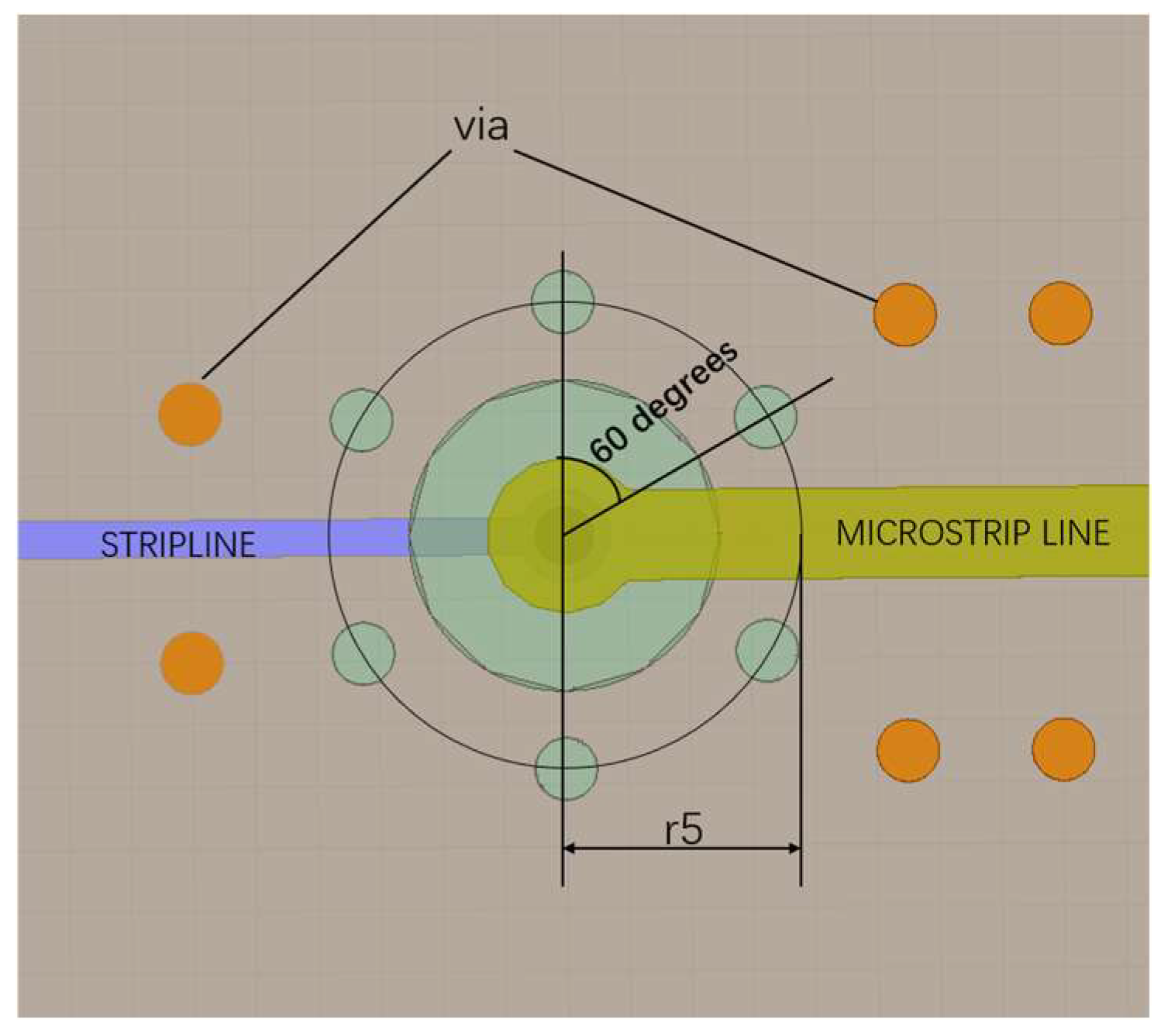
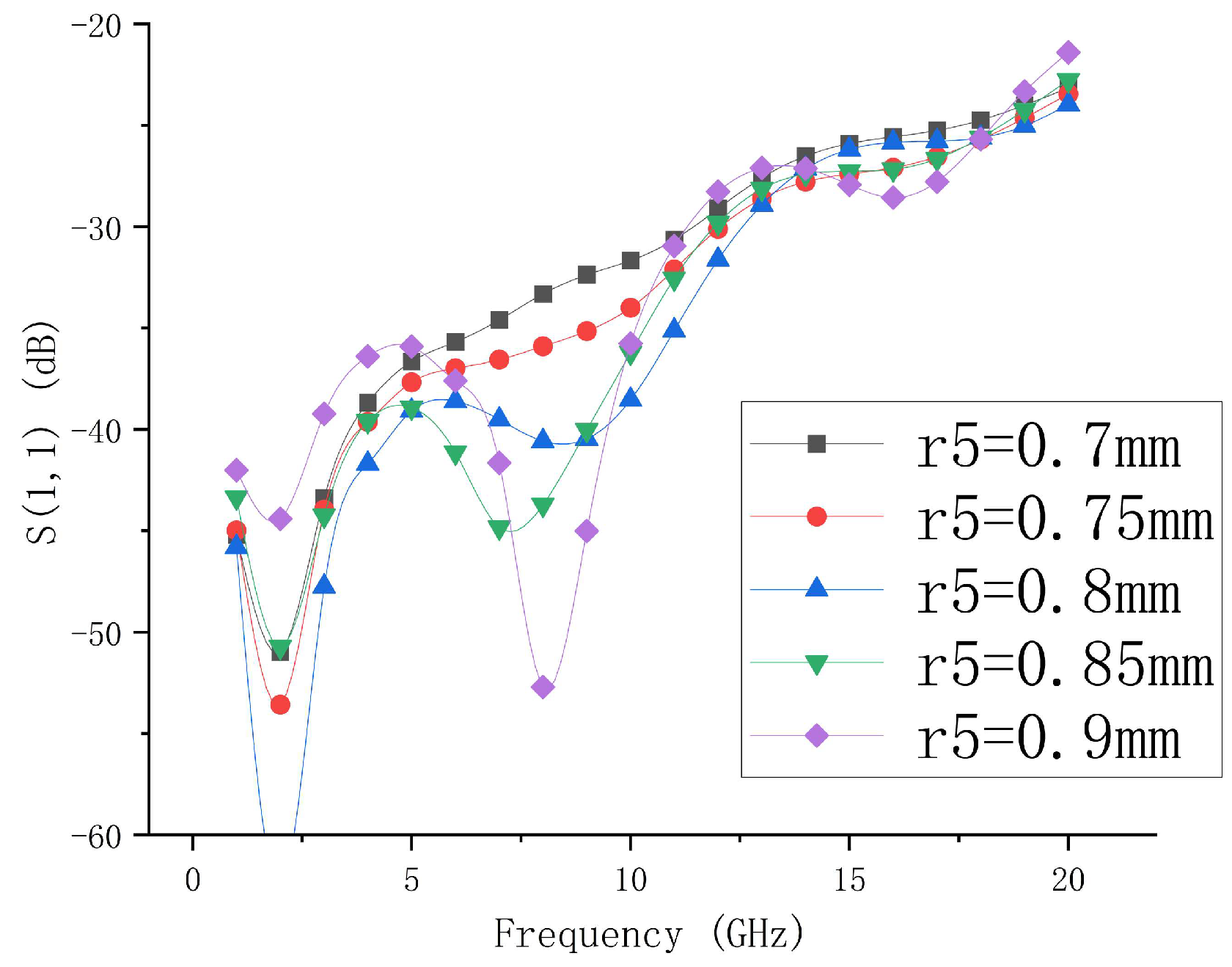
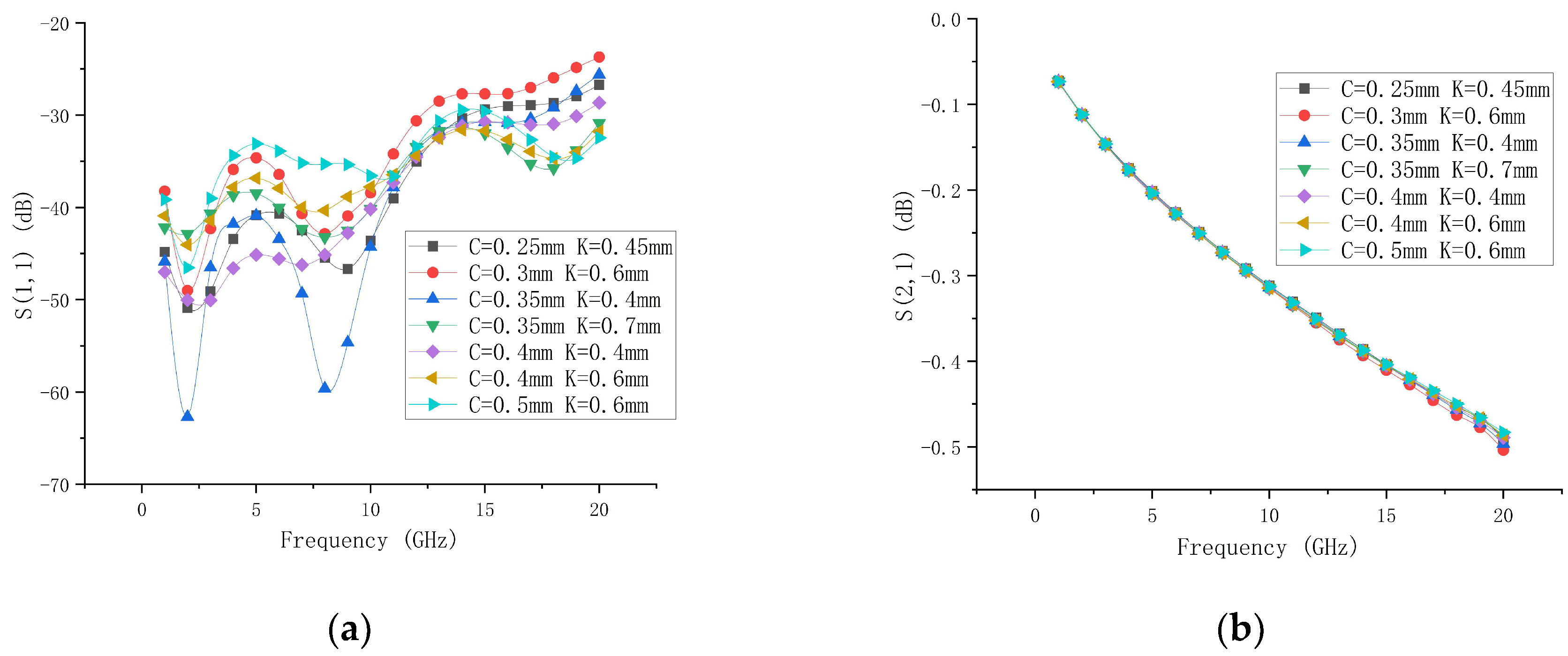
- Via Interconnection Design with Coaxial-Like Structure
- 2.
- Via Interconnect Structure Loaded with DGS Architecture
4. Results
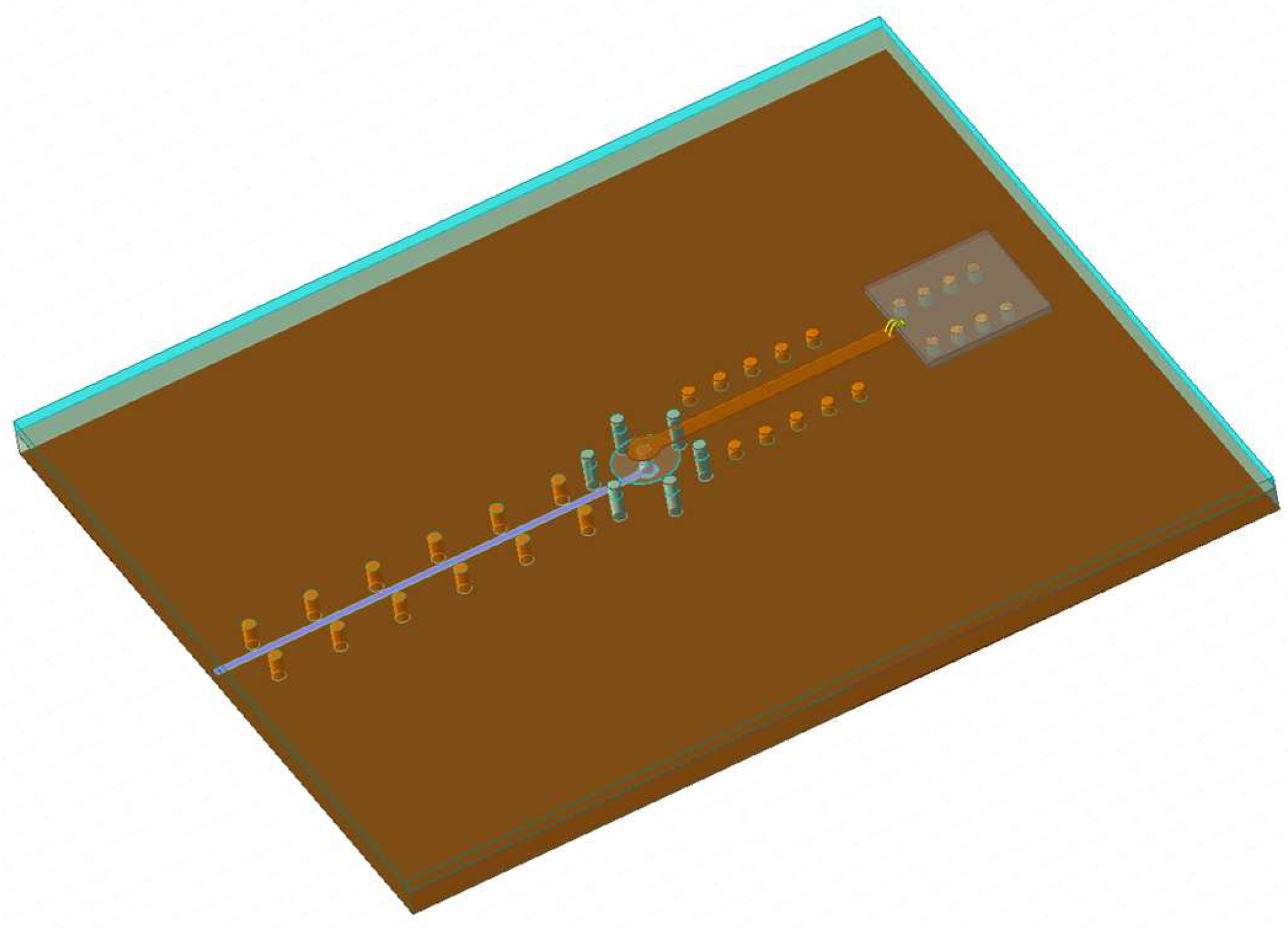
4.1. Full-Path Cascade Simulation and Broadband Performance Verification
4.2. Impact of T-Type Matching Networks and DGS on Transmission Performance of the Overall Interconnect Structure
5. Conclusions
Author Contributions
Funding
Data Availability Statement
Conflicts of Interest
References
- Khatri, R.; Yudhbir; Mounika, K.; Dhar, J.; Rao, C.V.N. Miniaturized LTCC based C-Band transmit receive integrated module for EOS-04 SAR payload. Curr. Sci. 2024, 126, 1019–1023. [Google Scholar] [CrossRef]
- Zhou, H.; Zhang, Y.; Cao, J.; Su, C.; Li, C.; Chang, A.; An, B. Research Progress on Bonding Wire for Microelectronic Packaging. Micromachines 2023, 14, 432. [Google Scholar] [CrossRef] [PubMed]
- Pfahler, T.; Scheder, A.; Vossiek, S.M. A Low-Loss Bond-Wire Interconnect Design with More Than 130 GHz Bandwidth Enabling an Ultra-Broadband Heterogeneous System Design. IEEE Trans. Microw. Theory Tech. 2024, 72, 505–515. [Google Scholar] [CrossRef]
- Gao, J. Research and Design of Miniaturized T/R Components Based on LTCC. Master’s Thesis, Nanjing University of Posts and Telecommunications, Nanjing, China, 2023. [Google Scholar]
- Umar, M.; Laabs, M.; Neumann, N.; Plettemeier, D. Bondwire Model and Compensation Network for 60 GHz Chip-to-PCB Interconnects. IEEE Antennas Wirel. Propag. Lett. 2021, 20, 2196–2200. [Google Scholar] [CrossRef]
- Wang, C.; Zhang, H.; Liu, H. Design of Vertical Interconnect Structures in 3D System-Level Packaging. Microprocessor 2018, 39, 10–13. [Google Scholar]
- Yildiz, Ö.F.; Thomsen, O.; Bochard, M.; Yang, C.; Schuster, C. Vertical Integration of Passive Microwave Components Using Functional Via Structures in LTCC Multilayer Substrates. IEEE Trans. Compon. Packag. Manuf. Technol. 2021, 11, 635–646. [Google Scholar] [CrossRef]
- Ge, P.; Zhu, H.-R.; Wang, J. Wire Bonding with Embedded Vertical Compensation and Novel BGA Interconnection Analysis for Multi-Layered System in Package. In Proceedings of the 2025 Asia-Pacific International Symposium and Exhibition on Electromagnetic Compatibility (APEMC), Taipei, Taiwan, 19–23 May 2025. [Google Scholar]
- Zhou, L.; Tang, W.; Pang, Y.; Wang, J.; Wang, B. Theoretical Calculation of Transmission Line Loss in Packaging Design. Electron. Packag. 2022, 22, 23–29. [Google Scholar]
- Luo, J.; Liu, S.; Yang, X.; Wang, J.; Li, Y. Design of a Non-Magnetized 5 T MRI RF Power Amplifier. J. Spectrosc. 2022, 39, 163–173. [Google Scholar]
- Zhu, Z. Research and Design of Broadband High-Efficiency Power Amplifiers. Master’s Thesis, Hangzhou Dianzi University, Hangzhou, China, 2025. [Google Scholar]
- Kumar, A.; Kartikeyan, M.V. Design and realization of microstrip filters with new defected ground structure (DGS). Eng. Sci. Technol. Int. J. 2017, 20, 679–686. [Google Scholar] [CrossRef]
- Liu, J. Application Research of DGS Structure in Common-Mode Noise Suppression for High-Speed Differential Interconnects. Master’s Thesis, Ningbo University, Ningbo, China, 2020. [Google Scholar]
- Wu, X.; Yang, X.; Ye, J.; Liu, G. Novel Prognostics for IGBTs Using Wire-Bond Contact Degradation Model Considering On-Chip Temperature Distribution. IEEE Trans. Power Electron. 2025, 40, 4411–4424. [Google Scholar] [CrossRef]
- Kung, M.-L.; Lin, L.-Y.; Lin, K.-H.; Cheng, H.-H.; Tien, Y.-H.; Ding, Y.-C. Build-Up Spiral and GND Vias for Improving Signal Integrity of Signal Core Vias. IEEE Trans. Compon. Packag. Manuf. Technol. 2021, 11, 2031–2034. [Google Scholar] [CrossRef]
- Tan, J.; Wang, Z. Design of Three-Dimensional Vertical Interconnect Structure Based on HTCC. China Institute of Electronics. In Proceedings of the 2024 National Microwave and Millimeter Wave Conference, Beijing, China, 16–19 May 2024; Key Laboratory of Ultra-High Frequency Complex Systems, University of Electronic Science and Technology of China: Chengdu, China, 2024; Volume 1. [Google Scholar]
- Lü, J.; Kan, Y.; Liu, S.; Xu, M.; Tang, J.; Cheng, H. Research on Ultra-Wideband Interconnect Technology for 3D-SiP Modules. Res. Prog. Solid-State Electron. 2025, 45, 51–57. [Google Scholar]


Disclaimer/Publisher’s Note: The statements, opinions and data contained in all publications are solely those of the individual author(s) and contributor(s) and not of MDPI and/or the editor(s). MDPI and/or the editor(s) disclaim responsibility for any injury to people or property resulting from any ideas, methods, instructions or products referred to in the content. |
© 2026 by the authors. Licensee MDPI, Basel, Switzerland. This article is an open access article distributed under the terms and conditions of the Creative Commons Attribution (CC BY) license.
Share and Cite
Yao, J.; Yu, S.; Huang, J.; Chen, C. Design and Optimization of LTCC Broadband Interconnect Structures for Bare-Chip Integration. Electronics 2026, 15, 194. https://doi.org/10.3390/electronics15010194
Yao J, Yu S, Huang J, Chen C. Design and Optimization of LTCC Broadband Interconnect Structures for Bare-Chip Integration. Electronics. 2026; 15(1):194. https://doi.org/10.3390/electronics15010194
Chicago/Turabian StyleYao, Junhao, Shenglin Yu, Jianlin Huang, and Chunlei Chen. 2026. "Design and Optimization of LTCC Broadband Interconnect Structures for Bare-Chip Integration" Electronics 15, no. 1: 194. https://doi.org/10.3390/electronics15010194
APA StyleYao, J., Yu, S., Huang, J., & Chen, C. (2026). Design and Optimization of LTCC Broadband Interconnect Structures for Bare-Chip Integration. Electronics, 15(1), 194. https://doi.org/10.3390/electronics15010194


