Article

Design of a New Busbar for VFTO Suppression and Analysis of the Suppression Effect

1
School of Electrical and Electronic Engineering, Hua Zhong University of Science and Technology (HUST), Wuhan 430074, China
2
China Electric Power Research Institute Co., Ltd., Wuhan 430074, China
3
School of Automation, Wuhan University of Technology, Wuhan 430070, China
*
Author to whom correspondence should be addressed.
Electronics 2025, 14(9), 1815; https://doi.org/10.3390/electronics14091815
Submission received: 20 March 2025 / Revised: 15 April 2025 / Accepted: 24 April 2025 / Published: 29 April 2025

Abstract

:
Very fast transient overvoltage (VFTO) is characterized by short wavefront time, high amplitude and wide frequency. VFTO poses a threat to the safe operation of power equipment. In order to suppress the harmful effects of VFTO transmission on power equipment, a new type of busbar based on the structure of “inductance + resistance” has been designed, which is called a “damping busbar”. In this study, the equivalent circuit of a damping bus including spurious parameters was developed. These stray parameters are formed between the GIS enclosure and the damping bus, and between the disk insulators and the damping bus. A damping bus simulation model was established based on the equivalent circuit to carry out analysis of the relationship between the structural parameters of the damping bus and the inductance generated by the damping bus. The simulation results showed that the number of turns plays a decisive role in bus inductance, and the relationship between the number of turns and inductance is approximately linear. Comparative analysis of multiple waveforms was carried out before and after the addition of damping buses to the GIS on a 550 kV test rig. The test data showed that the average amplitude of VFTO decreased by 20.36% after the installation of the damping bus, the number of breakdowns decreased by about 66.7%, and there was no obvious high frequency in the measured waveform after installation. In short, the damping busbar had a good suppression effect on the amplitude and frequency of VFTO, and reduced the number of breakdowns. This technique provides a novel solution for VFTO suppression.

1. Introduction

VFTO is a phenomenon of voltage fluctuation in power systems within very short time periods, usually occurring during the operation of gas-insulated switchgear (GIS). VFTOs have extremely short rise times, typically in the nanosecond range, and can reach hundreds of MHz or even GHz. This overvoltage is caused when a circuit breaker or disconnect switch in the GIS is operated. Arc reignition and multiple breakdowns occur during operation, leading to rapid voltage changes and reflection and superposition of electromagnetic waves, resulting in the formation of VFTO. The amplitude of the VFTO is usually high, and can be several times the rated system voltage or even higher. This is the reason VFTOs pose a threat to the insulation of electrical equipment [1,2,3,4,5].
Several of the hazards that VFTOs produce on a power system may be identified as follows:
  • The high amplitude and rapid rise time of VFTO can cause impacts on the insulation system of electrical equipment, leading to insulation deterioration and even breakdown [6,7,8].
  • The high-frequency component of VFTO generates strong electromagnetic interference (EMI) in the power system, which affects the operation status of secondary equipment [9,10,11].
  • Transformer windings are deformed or damaged due to mechanical stress on the transformer windings caused by VFTO [12,13].
The above hazards not only increase the maintenance cost of the power system, but also may cause large-scale power outages, affecting the safe operation of the power system.
The following methods are currently the conventional means of suppressing VFTOs:
  • VFTO generation and propagation is reduced by optimizing the design of GIS equipment; for example, by using low inductance bus structures, increasing damping resistors, etc. [14,15,16].
  • The VFTO amplitude is suppressed by metal oxide arresters (MOAs) [17,18,19,20].
  • The wavefront steepness of the VFTO is flattened by the capacitance which is generated by the overhead line [21,22,23,24].
However, these methods still have limitations in practical application. For example, although the method of optimizing the design of GIS equipment can effectively reduce the generation of VFTOs, it is costly and difficult to retrofit existing equipment. Although an MOA can limit the amplitude of VFTO, its response speed is limited and it cannot completely suppress the high-frequency part of VFTO. The steepness of VFTO is suppressed by overhead lines to some extent, but the transient attenuation is weakened beyond a certain length, and the decline tends to level off. A comparison of the common VFTO suppression methods mentioned above is shown in Table 1.
In response to the shortcomings of the existing VFTO suppression methods, a new type of busbar with an “inductor + resistor” structure has been designed, which is called a “damped busbar”. A damping busbar utilizes the characteristic that the busbar itself is an inductor, and the suppression of VFTO propagation is achieved by mechanical processing on the basis of a conventional busbar and the addition of a non-inductive resistor. In this study, an equivalent analytical model of a damping bus with stray parameters was established based on the structural characteristics of the damping bus. Relying on the equivalent analytical model, damping bus parameters were calculated, and a damping bus simulation model built. The current throughput capacity and insulation properties of the damped busbar were analyzed based on simulation modeling. Finally, the damping busbar’s effect on VFTO suppression was verified on a 550 kV GIS test rig.

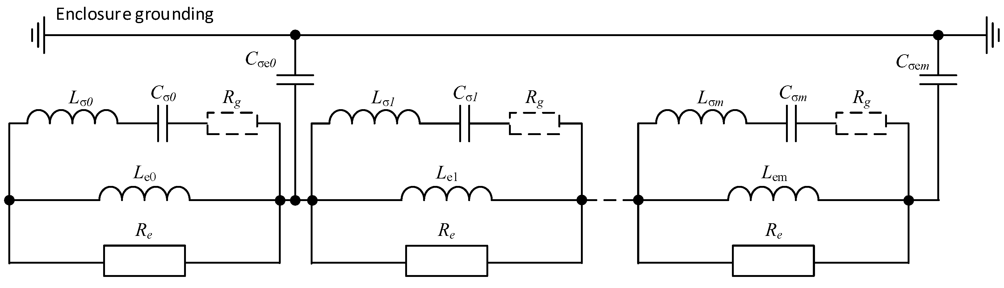
2. Analysis of Damping Busbar Design and Suppression Mechanism

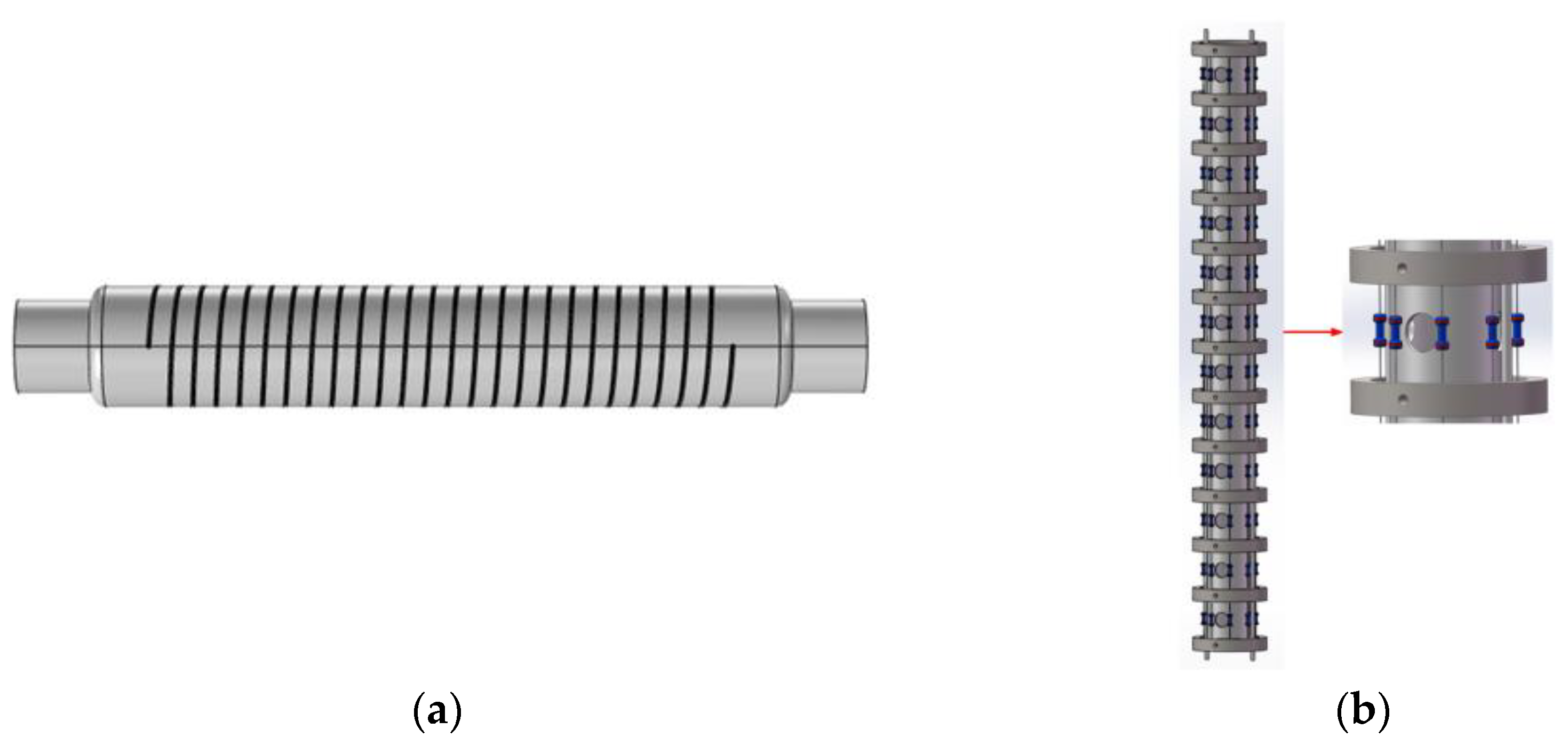
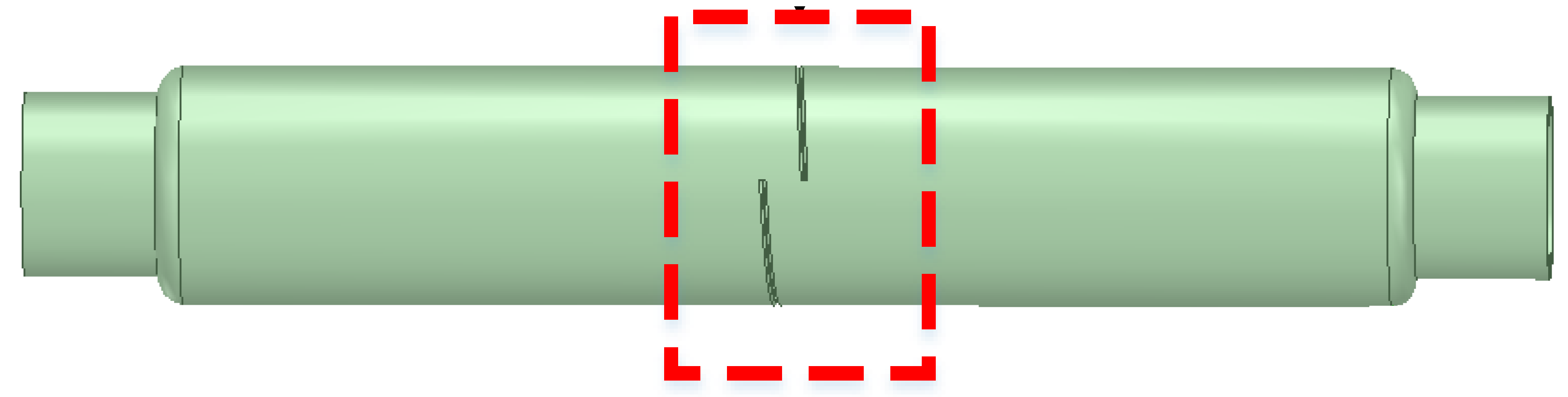
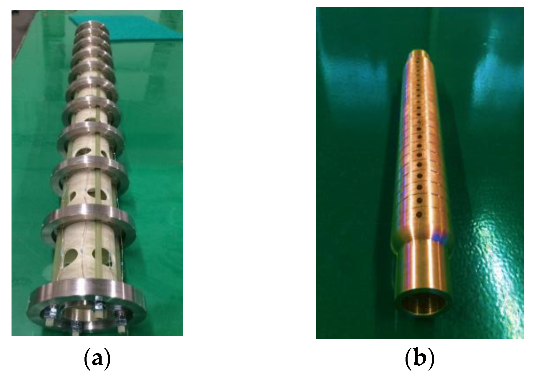
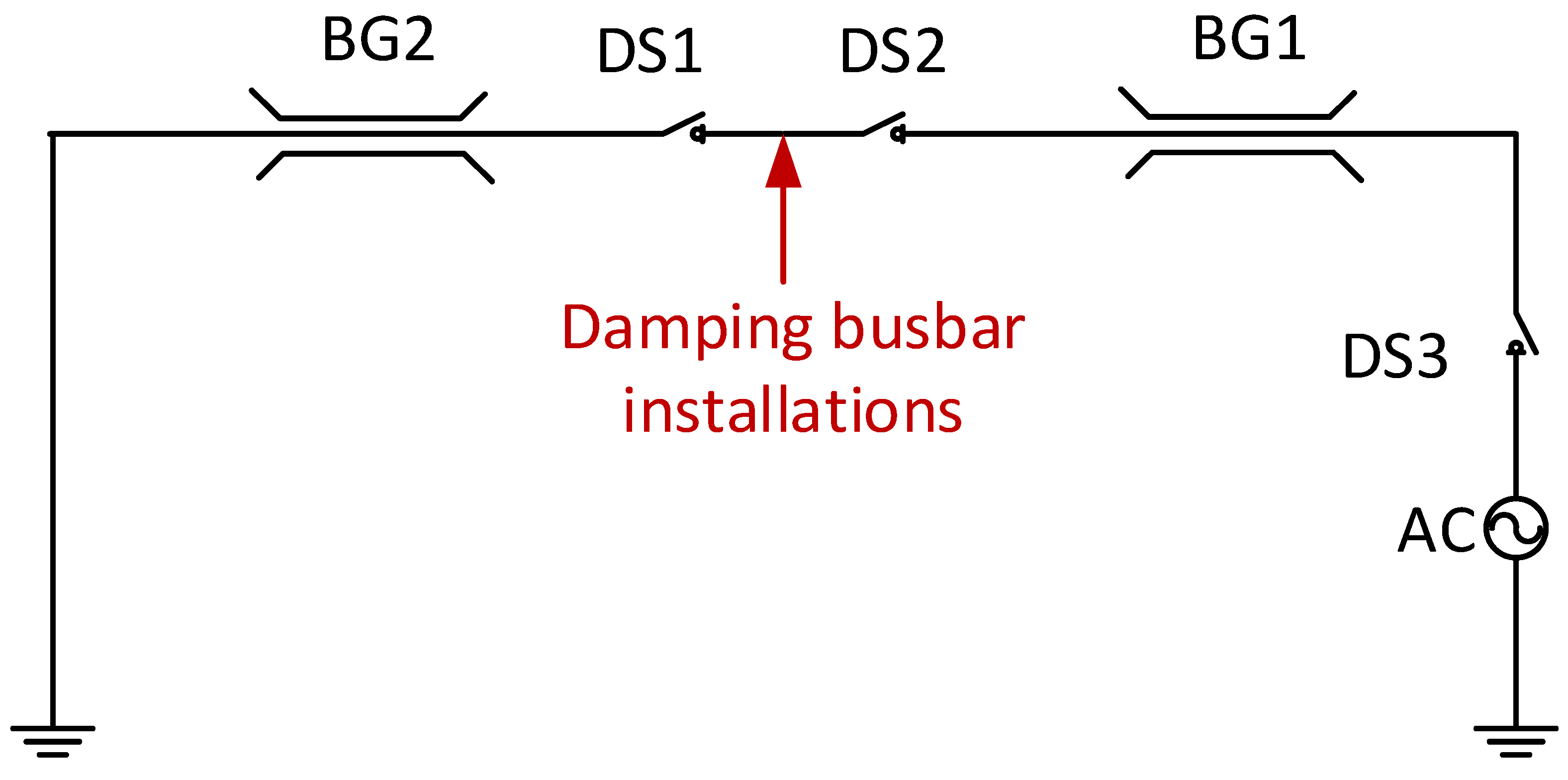
2.1. Structure Design

The structure of the damping bus is shown in Figure 1. The conventional busbar is machined into a spiral shape, as shown in Figure 1a [25,26]. The processed busbar tube forms a multi-turn inductive coil state. The circular spiral hollow on the busbar reduces its mechanical strength. Therefore, an epoxy support member is added inside the busbar to enhance the mechanical strength of the damping busbar, and a number of radial grooves are provided around it. Multiple non-inductive damping resistors are mounted in the grooves of the epoxy supports. The purpose of installing a non-inductive resistor is to allow the resistor to absorb energy and thus achieve suppression of the VFTO amplitude. The epoxy supports and resistors are shown in Figure 1b.
The damping busbar is hollowed out into a skeletonized slot by a spiral method, and the slot gap that is hollowed out becomes a discharge gap, so it exhibits strong inductive characteristics under high frequency conditions. The schematic cross-section of the damping busbar spiral is shown in Figure 2. The distance of the discharge gap near the outer side of the spiral tube is much larger than the inner gap distance. The insulation capability of the GIS duct enclosure is enhanced by this design. Because this design ensures that the gas discharge channel for the turn-to-turn breakdown of the overvoltage through the damping busbar is on the inside of the spiral tube, the effect of sparks on the outside of the damping busbar is minimized.

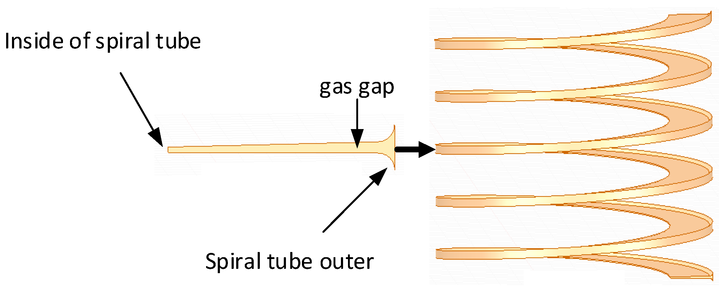
2.2. Suppression Mechanism

Installation of resistance, inductance or capacitance are the three most common means of suppressing overvoltage. A damping busbar utilizes the inductance of the wire itself to achieve overvoltage suppression. In this section, we analyze the working mechanism by which a damping busbar suppresses VFTO, based on traveling wave theory.
Figure 3 shows a schematic of a traveling wave through an inductor. The busbar itself has an inductance, so the busbar in Figure 3 is represented by Z1, and Z2 represents the load. According to Peterson’s law, when an infinitely long right-angle voltage u 1 traveling wave passes through an inductor, its voltage u 2 for the amplitude can be expressed as:
u 2 = i 2 Z 2 = 2 Z 2 Z 1 + Z 2 u 1 ( 1 e t τ L ) = a u 1 ( 1 e t τ L )
In Equation (1), τ L represents the time constant of the loop as L / ( Z 1 + Z 2 ) , and a represents the voltage refraction coefficient in the absence of inductance as 2 Z 2 / ( Z 1 + Z 2 ) . The wavefront steepness changes from that of an infinitely long right-angle wave, so that:
a = d u 2 d t = 2 Z 2 Z 1 + Z 2 u 1 1 τ t e t τ L = 2 Z 2 u 1 L e t τ L
The equivalent circuit of the VFTO wave as it passes through the damping bus is shown in Figure 4.
In Figure 4, u1 represents the input VFTO wave, u2 represents the voltage at node A, and iL and i2 represent the incident currents flowing through L and Z2, respectively. R and L represent the damping resistance and inductance, respectively, of the damping bus. Z1 represents the wave impedance of the line between the isolation switch and the damping bus. Z2 represents the wave impedance of the line after the damping bus. Z1 and Z2 are formed by equating the distributed parameters of wave propagation to the centralized parameters to form an impedance, and they are real numbers. According to the previous analysis of the wave through the inductance, it can be seen that the equivalent impedance Z outside the inductance L can be expressed as:
Z = ( z 1 + z 2 ) / / R = R ( z 1 + z 2 ) R + z 1 + z 2
τ = L Z = L ( R + z 1 + z 2 ) R ( z 1 + z 2 )
We then solve for the current flowing through the inductor, as follows:
i L ( t ) = 2 u 1 z 1 + z 2 ( 1 e t τ )
After the VFTO wave passes through the damping bus, the current and voltage across the impedance Z2 are expressed as:
i 2 ( t ) = i L + L R d i L d t = 2 u 1 z 1 + z 2 ( 1 R R + z 1 + z 2 e t τ ) = 2 z 1 z 1 + z 2 i 1 ( 1 R R + z 1 + z 2 e t τ )
u 2 ( t ) = i 2 z 2 = 2 u 1 Z 2 Z 1 + Z 2 ( 1 R R + z 1 + z 2 e t τ )
The steepness of the voltage wave is expressed as:
a = d u 2 d t = 2 u 1 R 2 z 2 L ( R + z 1 + z 2 ) 2 e t τ
The maximum steepness of the VFTO across the inductor is:
a max = d u 2 d t | t = 0 = 2 u 1 R 2 z 2 L ( R + z 1 + z 2 ) 2 ( k v / u s )
The wave impedance of a coaxial GIS bus is calculated by the following equation:
Z = μ / ε 2 π ln ( r 2 r 1 )
In Equation (10), r 1 and r 2 represent the inner and outer radii, respectively, of the GIS bus conductor. As the voltage levels are the same, the voltage on impedance Z2 after passing through the damped bus is:
u 2 ( t ) = i 2 z 2 = ( 1 R R + z 1 + z 2 e t τ ) u 1
The SF6 is used as an insulating medium for GIS, and its magnetic permeability is approximately equal to the vacuum magnetic permeability, as μ ≈ μ0 = 4π × 10−7 H/m. Taking the 550 kV GIS bus wave impedance of 120 Ω as an example, the voltage and steepness behind the bus after the addition of the damping bus can be expressed as:
a = 2 u 1 R 2 z 2 L ( R + z 1 + z 2 ) 2 e t τ = 240 R 2 L ( R + 240 ) 2 u 1 e t / τ
τ = L Z = L ( R + 240 ) 240 R = L 240 + L R
It can be seen from Figure 4 that both the magnitude and steepness of VFTO decrease with an increase in inductance, and the effect of resistance on the magnitude and steepness of VFTO exhibits a non-monotonic influence property. This means that an interval of values exists within which VFTO amplitude and steepness suppression may be optimized. A resistance interval of (0–300) Ω is used for the calculations in this paper. The calculations showed that the VFTO is optimally suppressed at a resistance value of (100–120) Ω.
Next, analysis of the effect of damping bus resistance and inductance on VFTO amplitude suppression and steepness suppression is carried out using the separated variable method. Substituting different inductors and resistors into Equations (11) and (12) to analyze the variation of node voltage and wavefront steepness, the trend is obtained, as shown in Figure 5.

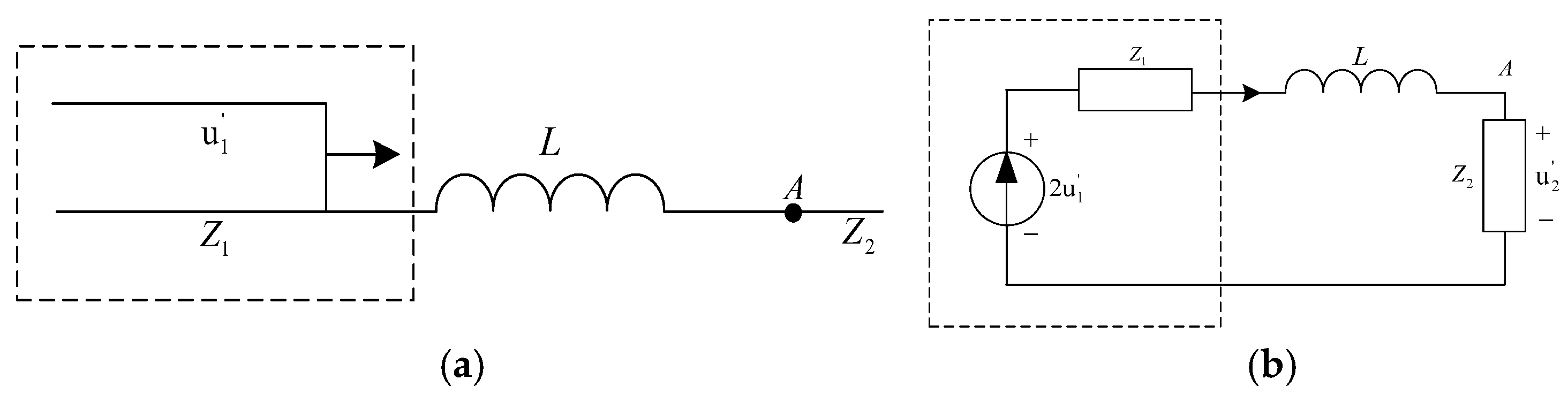
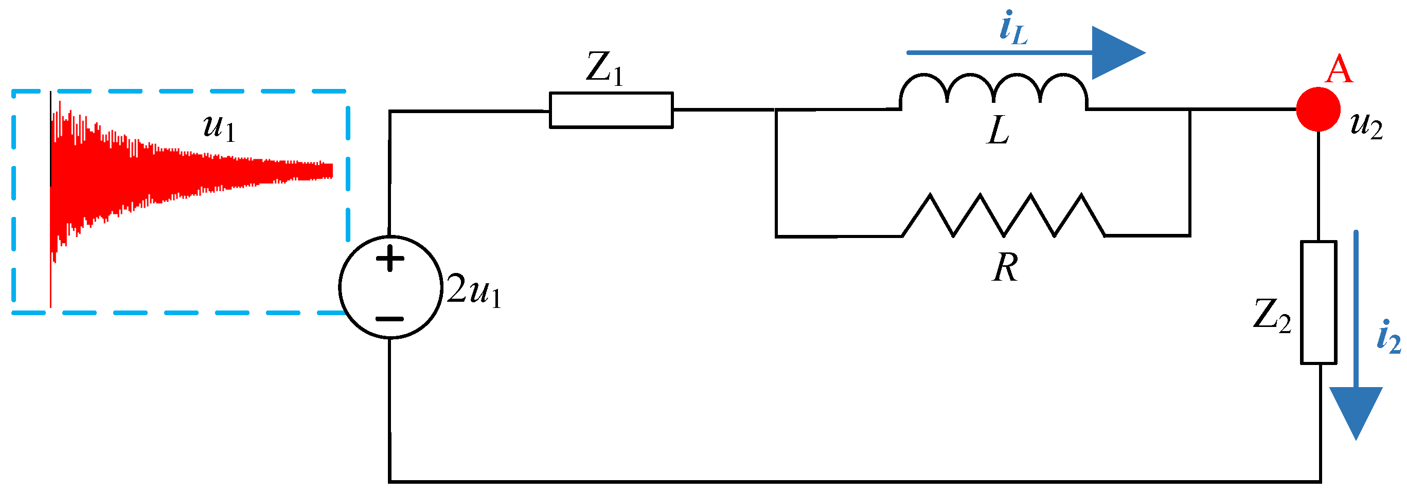
2.3. Equivalent Circuit Parameter Analysis

Next, the damping busbar is installed in the GIS. Considering the existence of stray inductance and capacitance between the GIS shell and the damping busbar, and between the damping busbar and the tub insulator, the equivalent circuit of the damping busbar is established as shown in Figure 6.
In Figure 6, Le represents the equivalent inductance per turn of the coil. Re represents the parallel resistance per turn of the coil. Each turn of the damping busbar coil is uniformly machined so that the turn inductances are all equal, that is, Le0 = Le1 = … = Lem. Cσm and Lσm represent the turn-to-turn stray capacitance and stray inductance, respectively. Because the inductance at the two ends of the damping busbar connecting the pot insulator portion is not equal in magnitude to the uniform spiral tubular turn-to-turn inductance in the center, it is denoted by Le0 and Lem. Cσe0 and Cσem represent the stray inductance between the ends of the damping bus and the housing. Rg represents the gap breakdown impedance. The gap breakdown impedance is shown as a dashed line in Figure 5, as the gap breakdown of the damped bus under VFTO conditions is uncertain.
Capacitance is defined as C = Q / ( V 1 V 2 ) , for n conductors, by the potential superposition theorem:
Q 1 Q 2 Q n = C V 1 V 2 V n = C 11 C 12 C n 1 C 12 C 22 C n 2 C 1 n C 2 n C n n V 1 V 2 V n
In Equation (14), Qi denotes the charge of the i-th conductor, and C is the Maxwell capacitance matrix, which describes the relationship between the charge of the i-th conductor and the voltages of all the conductors in the system. For n conductors, the Maxwell capacitance matrix can be expressed as:
C = i = 1 n C m 1 i C m 12 C m 1 n C m 21 i = 1 n C m 2 i C m 2 n C m n 1 C m n 2 i = 1 n C m n i
In Equation (15), Cmni is the stray capacitance resulting from the charge accumulation of the n-conductor and the i-conductor. The Maxwell’s capacitance matrix is used to solve for the relationship between the stray capacitances of the damping buses.
Neglecting the non-uniformity of the current distribution in the cross-section of the conductor under low-frequency conditions, the value of inductance at this time can be expressed as:
L = 1 i 1 s ( B d s ) d s
Under very high frequency conditions, the current is almost entirely concentrated in the surface layer of the conductor, when the skinning depth can be expressed as:
δ s d = 1 π f μ σ
In Equation (17), δ s d indicates the skinning depth in m. f is the excitation frequency in Hz. μ is the magnetic permeability in H/m. σ is the electrical conductivity in S/m. Because of the skinning effect, Equation (17) cannot be calculated directly; however, the effective cross section of the current can be calculated by approximation of the skinning depth, which is then brought into Equation (18):
L = 2 π ( a + 1 ) i 2 ( B 1 π f μ σ d r ) d i
From the above equation, it can be seen that the inductance L of the damping bus under high frequency conditions is not only related to the conductor structure but is also affected by the excitation characteristics, and inductance decreases with the increase in current frequency.
Due to the extremely short time of VFTO action, the gap SF6 breakdown process can be viewed as an arc discharge process. An exponential model is used to describe the change in resistance when the damped bus gap is undergoing breakdown, as in the following equation:
R v = R 0 e t τ g + R a ,   t t 0
In Equation (19), Ra = 0.5 Ω for static arc resistance, and R0 = 1012 Ω for isolation switch gap insulation when in a high resistance state. τg denotes the breakdown time of the gap. The SF6 breakdown time is very short, usually at the ns level, so τg is also very small. During SF6 gas breakdown, gas gap resistance can take the value of 0.5 Ω. In this paper, a 550 kV voltage level is used as an example to calculate the internal damping busbar parameters of GIS. Assuming that the damping bus processing involves 25 turns, the specific calculation parameters are shown in Table 2.

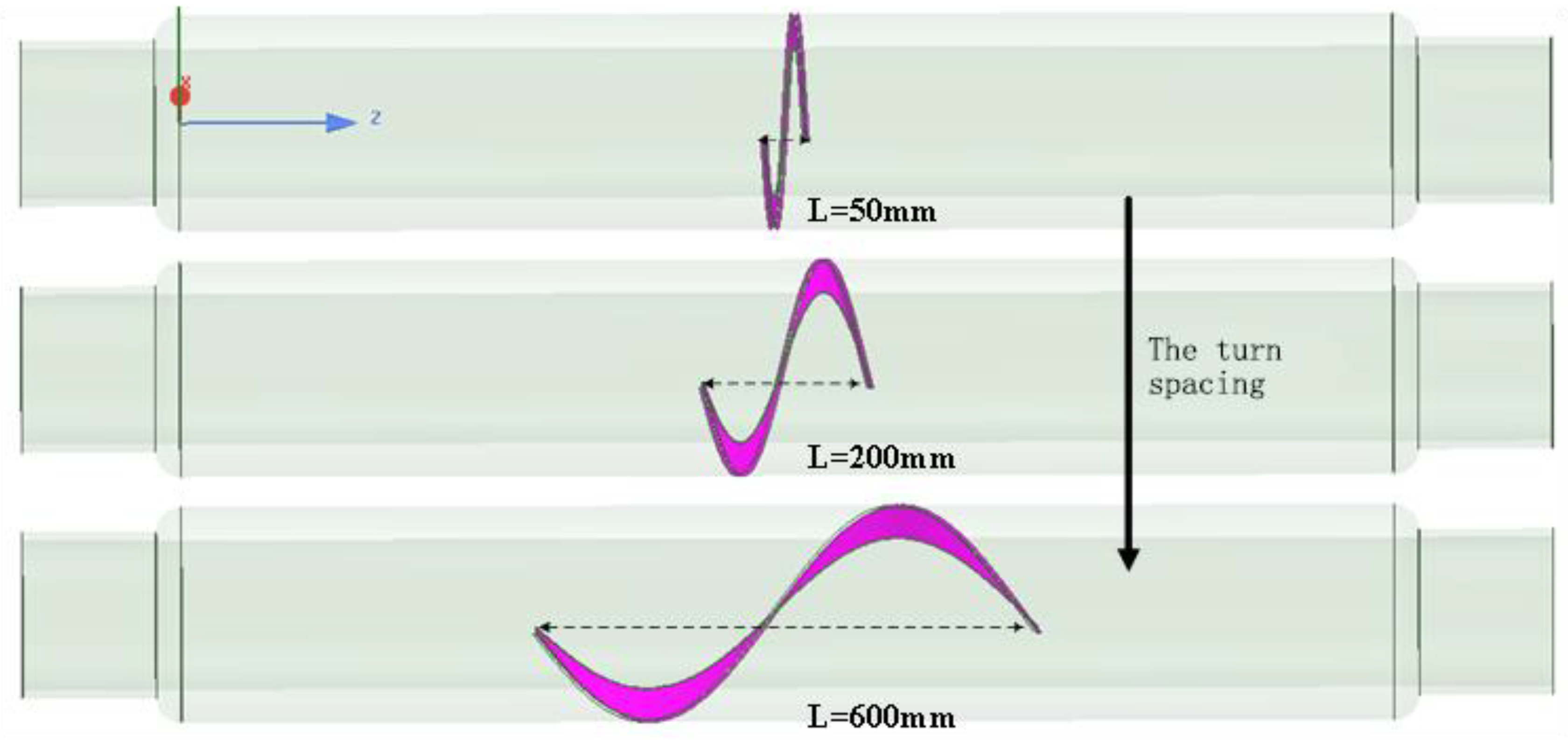
3. Structural Optimization Design of Damping Busbar

In this paper, an aluminum busbar for GIS at a 550 kV voltage level is used as an object to analyze the effect of variations in turn spacing and numbers of turns on the inductance value of a damped busbar at a certain length (1451 mm).

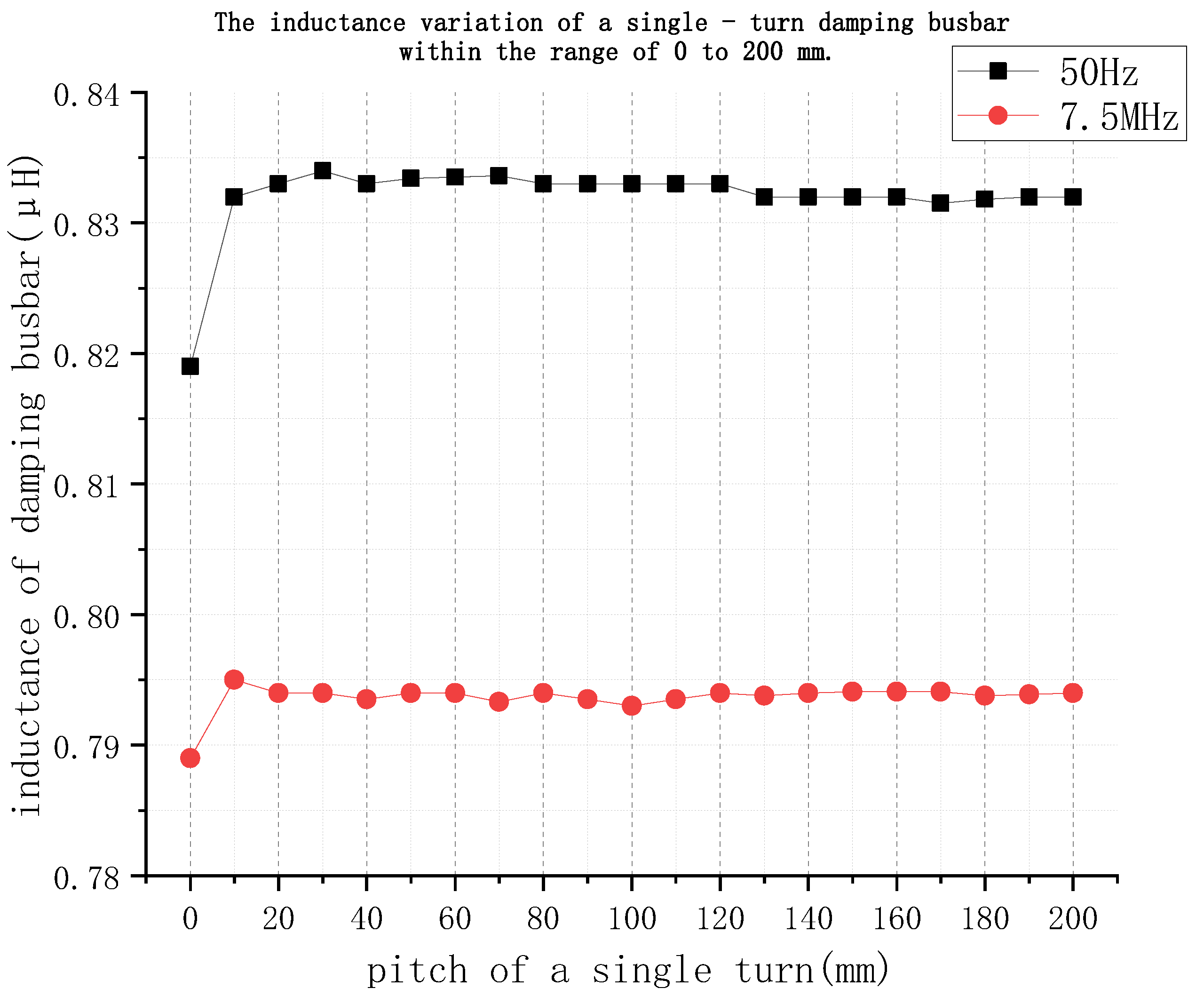
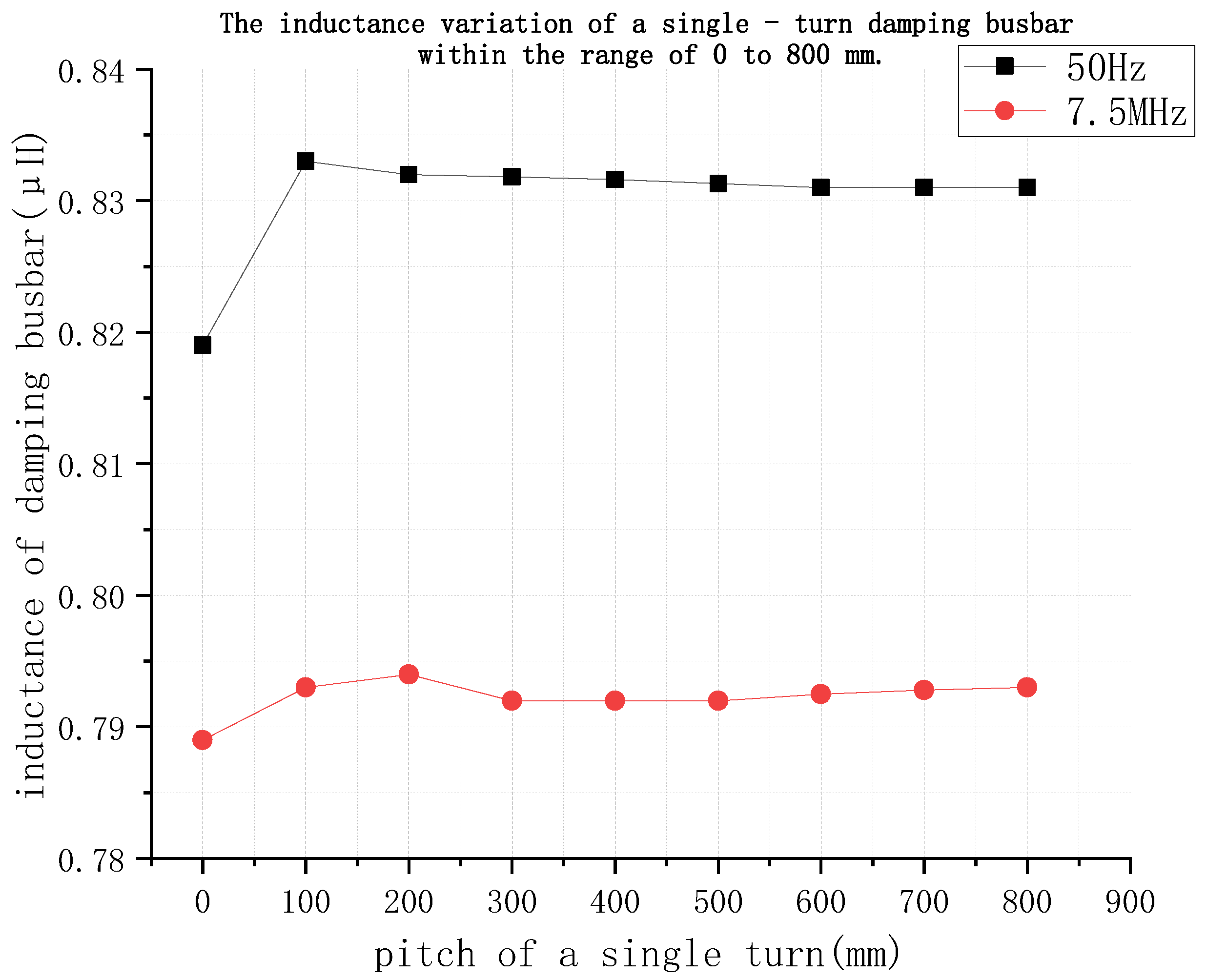
3.1. Analysis of the Effect of Turn Spacing on Inductance

A spiral cutting surface is made symmetrically from the geometric center of the damping busbar to both sides to form one turn spiral, constituting a single-turn damping busbar as shown in Figure 7.
Keeping the shape of the spiral skeletonized cross-section constant, the turn spacing is continuously increased, as shown in Figure 8. Finite element modeling for various different turn spacings is included, as follows:
  • Small increase in turn spacing between 0 and 200 mm.
  • Wide range of turn spacing between 200 and 800 mm.
Next, keeping all other conditions constant, finite element inductance calculations are carried out.
(1)
Inductance variation within 0~200 mm turns spacing
The model of the unprocessed bus is defined when the turn spacing is 0 mm. A single-turn damped bus model is then constructed with a small range of turn spacings by increasing the turn spacing by 10 mm each time from 0 to 200 mm. The inductance distribution curves of each model at industrial frequency and high frequency are shown in Figure 9.
It can be seen from Figure 9 that a small increase in the single-turn spacing has no effect on the inductance values of the damping busbar at IF or HF in the range of 0 to 200 mm. The inductance value floats around 0.833 μH at industrial frequency and 0.79 μH at high frequency. The inductance increases, but not significantly, when conventional busbars are machined into single-turn damped busbars.
(2)
Inductance Variation within 0~800 mm Turn Pitch
Damping busbars can be machined in the middle section of a busbar with a length of 1451 mm, increasing the range of single-turn helical machining by 100 mm per turn in the range of 0 to 800 mm. The same finite element method inductance calculations as above were performed for the damping bus for a large turn spacing range, and the results are shown in Figure 10. After increasing the turn spacing variation, the inductance of the damping bus remains almost unchanged for both the IF and HF inductances.
Comparison of the curves in Figure 10 reveals that the effect of single-turn processing on inductance is small for both turn spacing variations. The single-turn construction of the busbar does not change the path of the transmitted current on the busbar, and the inductive effect is not significant. Although single-turn spacing variations have a small effect on busbar inductance, the number of turns and the amount of turn spacing are inversely proportional over a fixed machinable length. Damping busbars can be processed with reduced turn spacing to obtain more turns, thus increasing the inductive effect of the busbars.

3.2. Analysis of the Effect of the Number of Turns on Inductance

Next, the damping busbar turn spacing is set to 50 mm and the number of turns is increased from 1 to 25. The same excitation imposition, meshing, and solution setup as above is used. The busbar material is aluminum (conductivity 3.8 × 10⁷ S/m), and the change of inductance of the busbar under industrial frequency and high frequency conditions is shown in Table 3.
According to the data in Table 3, it can be seen that with same amount of turn spacing and number of turns, the value of inductance under industrial-frequency excitation is greater than that under high-frequency excitation, and with an increase in busbar turns, the inductance of the busbar increases under both industrial frequency and high frequency conditions. In addition, regardless of whether there is industrial- or high-frequency excitation, the damping bus inductance shows a linear increase with the number of turns, and the inductance of the traditional spiral coil increases linearly with the number of turns of the coil, similar to the law. On this occasion, the damping bus can be seen as a large-size, high-current capacity of the coil.

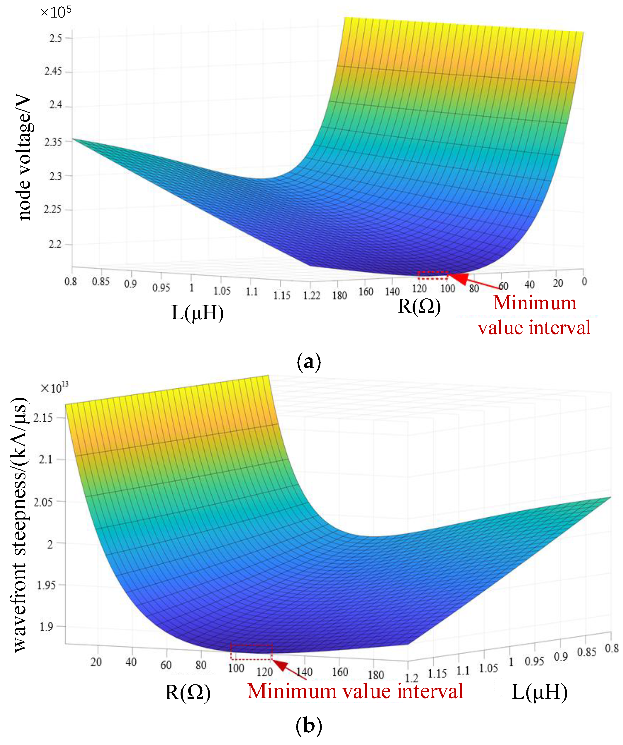
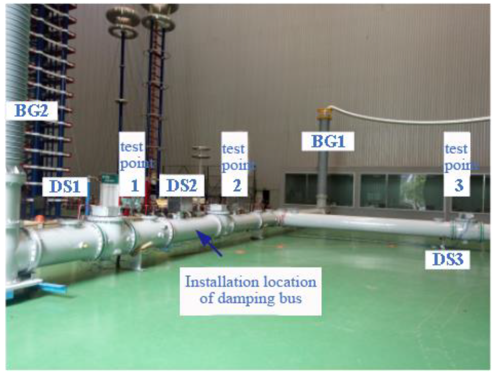
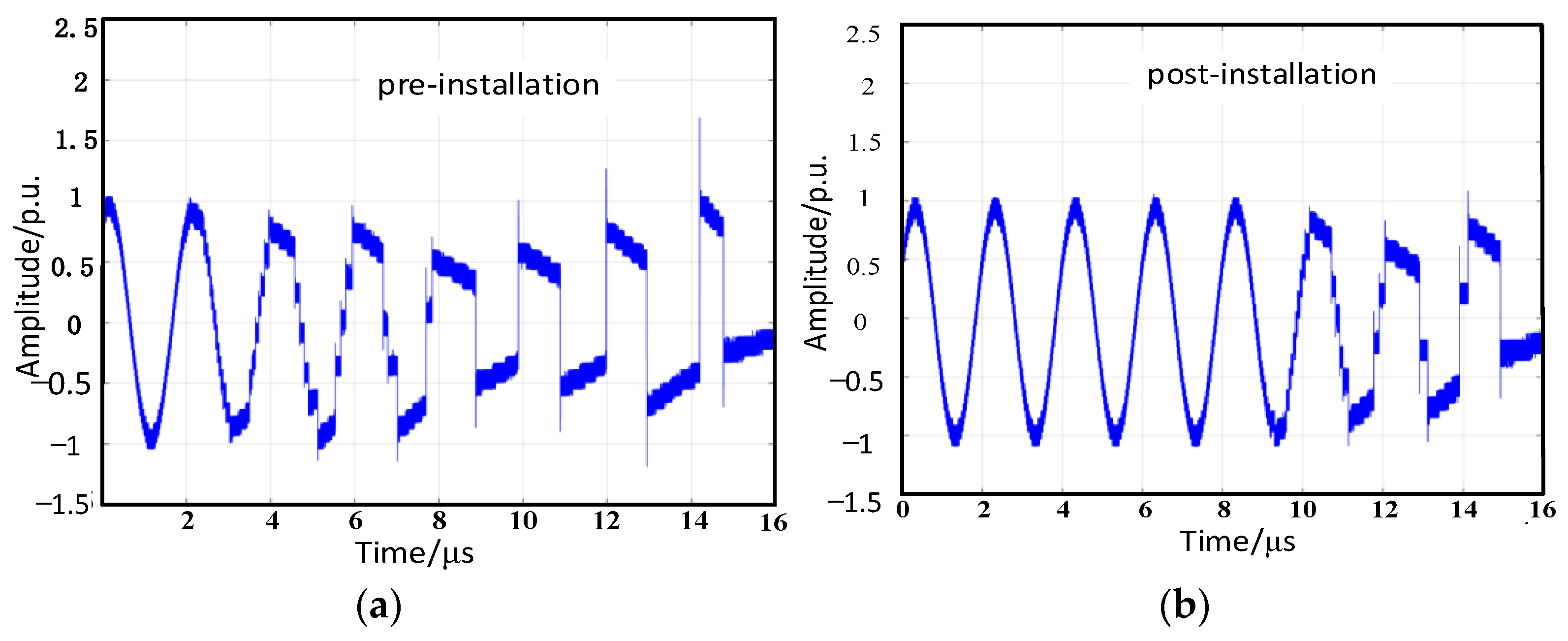
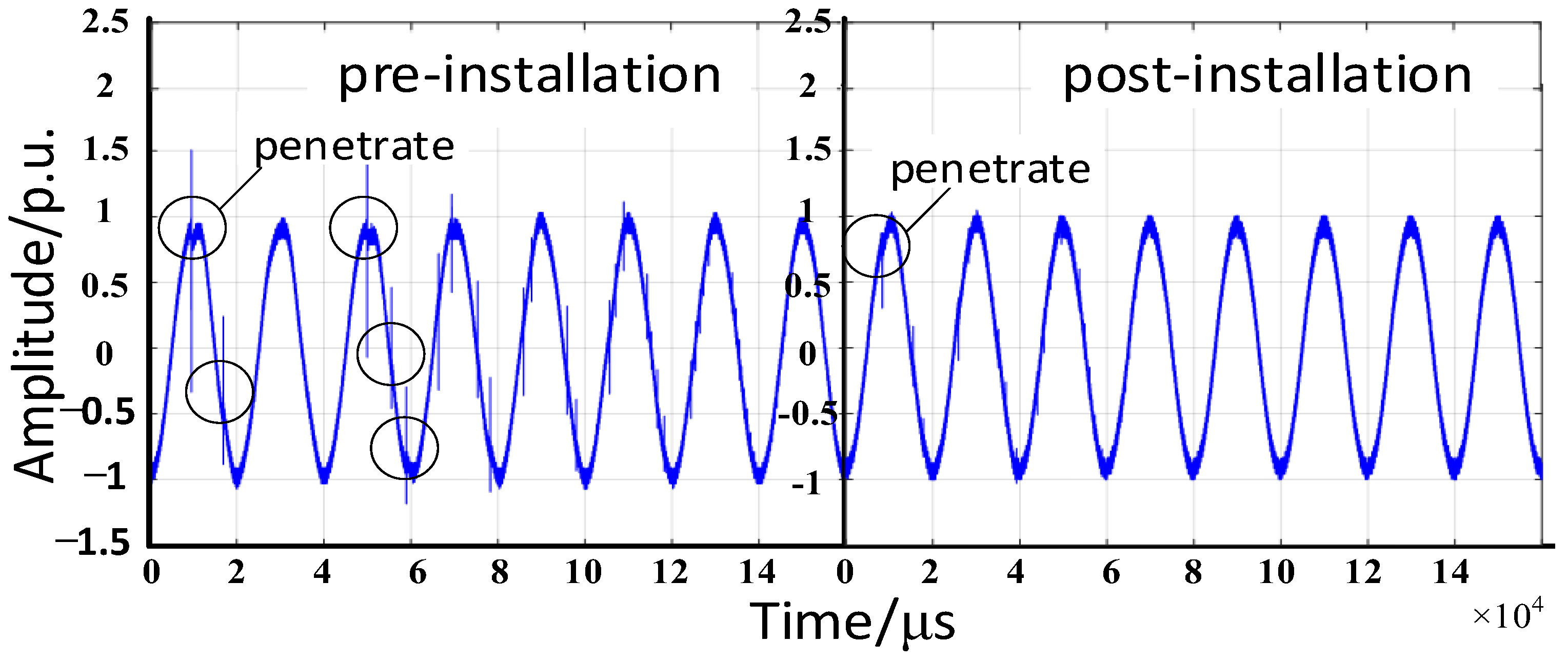
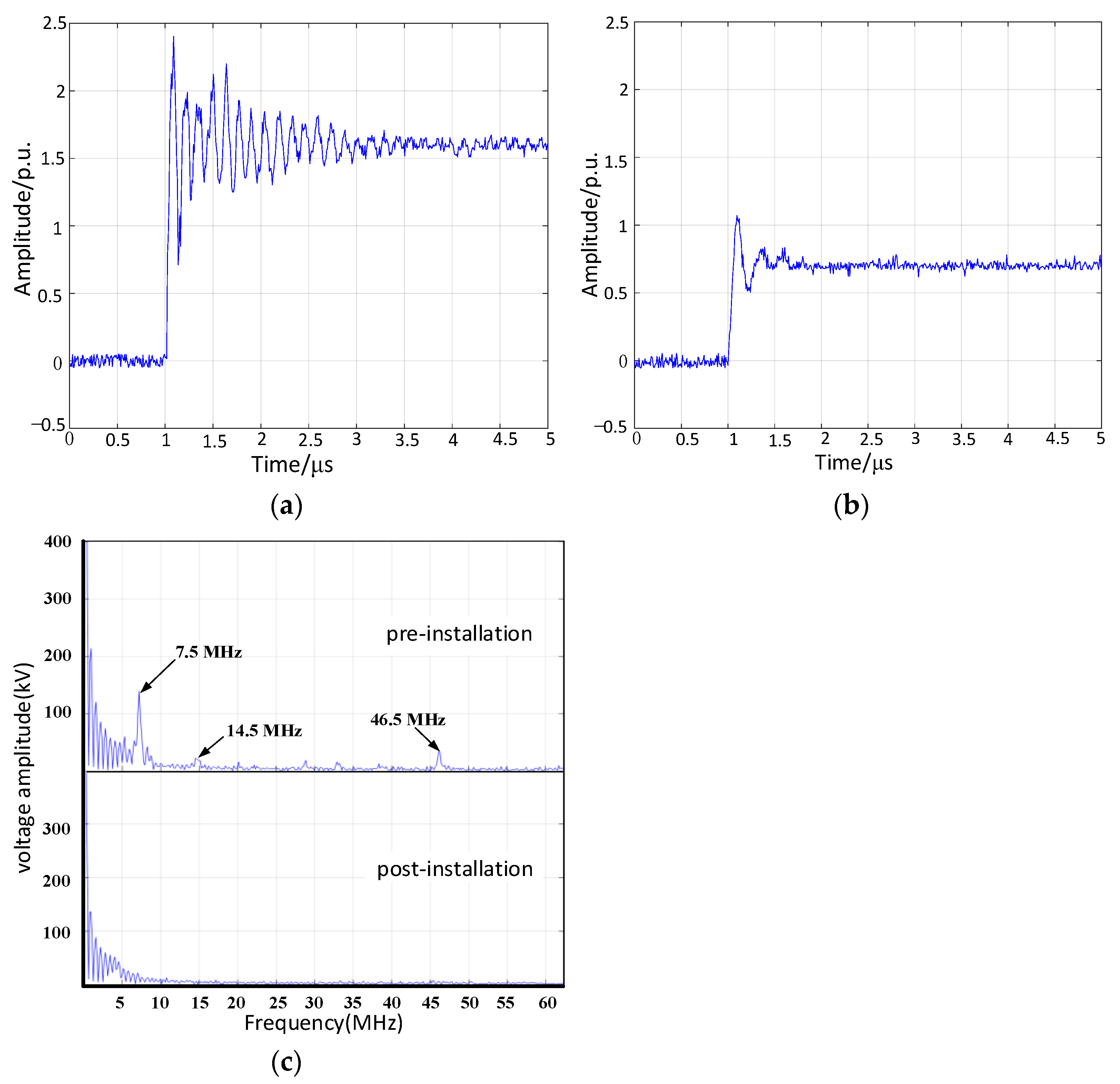
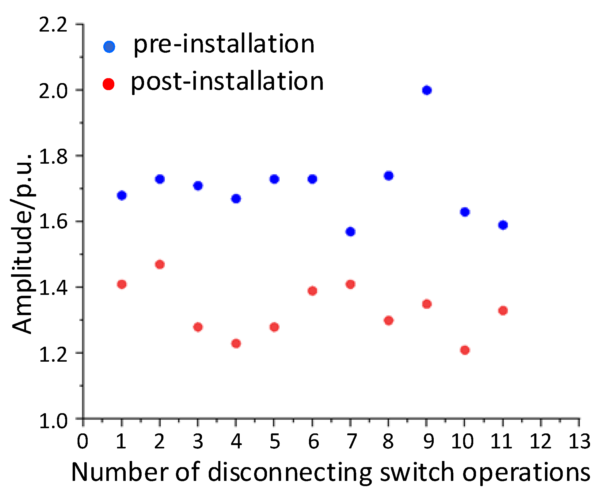
4. Analysis of Damping Busbar Effect on VFTO Suppression

The appearance of the damping busbar for 550 kV GIS obtained by actual processing is shown in Figure 11.
The electrical principle of the 550 kV verification test circuit is shown in Figure 12. In Figure 12, each piece of equipment is connected or enclosed in a GIS pipe, and AC stands for alternating-current power supply, which provides power for the whole test circuit and is used to simulate the generation of high-frequency over-voltage. BG1 and BG2 stand for GIS bushings, and DS1, DS2 and DS3 stand for disconnecting switches. The GIS pipe is used to simulate the branching of busbars, and the length of the pipe can be adjusted and dismantled. In addition, the test circuit includes grounding switches, busbars and other components. The length of the tubing between DS1 and DS2 is 9 m, and the length of the tubing between DS2 and BG1 is 14 m. Photographs of the validation test platform are shown in Figure 13.
The VFTO measurement system is mainly composed of three parts: a VFTO measurement sensor; a synchronized trigger device; and a waveform acquisition device with remote measurement and control computer (waveform recording.) The VFTO measurement adopts a window-type sensor based on the principle of capacitive voltage division, with measurement bandwidth ranging from 10 Hz to 204 MHz and a sampling accuracy of 0.05%, which meets the needs of VFTO measurement. The measurement system uses a synchronized trigger device to ensure the stability and synchronization of the measurement system. The synchronous trigger is 1 pps. The high-frequency radiation signal during the VFTO generation process controls the synchronous trigger device to generate a trigger signal, which is transmitted through optical fiber, converted optically and electrically, and recorded at each measurement point of the stable synchronous trigger oscilloscope. Waveform recording includes on-site recording and remote computer reading. The on-site acquisition device is placed in a shielded box, powered by an independent power supply, with strong anti-interference capability. A DLM2054 oscilloscope was used to record the field waveforms. The sampling frequency of the oscilloscope was set to 125 MHz, the length of the recorded waveforms was 1 s, and the accuracy of this oscilloscope was 0.05%. The computer controls the oscilloscope through a fiber optic transmission channel and remotely reads the waveforms stored in the oscilloscope, thus improving the efficiency and safety of testing.
The test first measured the VFTO appearing on the conventional GIS. Testing was then carried out again under the same working condition at the same observation point after adding the damping bus, to observe the damping bus’s suppression effect on the VFTO, and read the recorded VFTO waveforms with Xviewer software V1.0. Due to the large number of measured data, only the measured data of the isolating switch tripping operation are selected here to analyze the damping busbar’s suppression effect on VFTO. Figure 14 shows the VFTO full waveforms before and after the addition of the damping bus.
Figure 15 shows a comparison of breakdown times before and after the installation of the damping bus. Comparison of Figure 14 and Figure 15 shows that the amplitude and breakdown times of the VFTO are obviously suppressed after the installation of the damping bus. The specific data are shown in Table 4.
The single breakdown pulse waveforms before and after the addition of the damping bus are shown in Figure 16. Comparing Figure 16a,b, it can be seen that the amplitude of the single breakdown pulse waveform is significantly suppressed after the addition of the damping bus.
Figure 16c shows the spectral comparison of the single breakdown VFTO before and after the addition of the damping busbar. From the figure, it can be seen that the frequency of the VFTO is significantly reduced after the installation of the damping busbar. The data are shown in Table 5.
From the data in Table 5, it can be seen that the number of breakdowns and the amplitude of oscillations are reduced before and after the addition of the damping busbar, and the attenuation of the single and overall transient processes is accelerated. The high-frequency components of the VFTO are mainly 7.5 MHz, 14.5 MHz and 46.5 MHz before the addition of the damping busbar, while there is no significant high frequency after the installation of the damping busbar. It can be seen that the damping buses flatten the high-frequency component heads and tails of the VFTO wave as it passes through by enhancing the inductive effect, and the amplitude is reduced.
Plots of the test statistics for the suppression effect of VFTO under the condition of multiple tripping operations are shown in Figure 17. The effect of the number of test tripping operations on the VFTO suppression effect is random, and the suppression effect does not become more significant with the increase in the number of operations. According to the data in Figure 17, the amplitude of VFTO after the damping busbar is installed is significantly lower than that in the uninstalled state. The average amplitude of VFTO before installation is 1.67 p.u., and the average amplitude of VFTO after installation decreases to 1.33 p.u. After analyzing the ANOVA using independent samples t-test, the p-value is less than 0.001 and the difference in means is very significant; excluding the effect of randomness of VFTO amplitude on the statistical results, the damping busbar causes a 20.36% reduction in the average amplitude of the VFTO. The results are shown in Table 6.

5. Conclusions

In this paper, a new type of busbar is designed for VFTO suppression, which is called a “damped busbar”. A damped busbar is a traditional busbar hollowed out into a spiral-tube hollow coil to increase inductance, in which the hollow wire inside each turn of the coil is matched with the corresponding resistance, composed of “inductance + resistance” structure. In this work, we established a damped bus circuit model, carried out an analysis of the structural constraints of the damped bus, and finally conducted a test on the damped bus suppression effect. The following conclusions were obtained:
  • As ordinary busbar using 550 kV GIS platform was processed into a spiral damping busbar. After processing, its stray inductance was about 0.4 μH and its stray capacitance was about 0.18 nF.
  • The structural parameter that plays a decisive role in the inductance of the damping busbar is the number of turns. Whether under industrial-frequency or high-frequency excitation, when the length of the damping bus is certain, the higher the number of turns, the greater the bus inductance. The value of inductance under industrial-frequency excitation is greater than that under high-frequency excitation. Damping bus inductance increases approximately linearly with the number of turns, similar to the linear increase in inductance with the number of turns of a conventional helical coil.
  • The VFTO suppression effect of the damping busbar was systematically verified using a combination of simulation calculation and experimental verification. The test data showed that the average amplitude of VFTO decreased by 20.36% after addition of the damping busbar, the number of breakdowns decreased by about 66.7%, and there was no obvious high frequency after the installation of the damping busbar. These data show that the damping busbar has a good suppression effect on the amplitude and frequency of VFTO, and reduces the number of breakdowns.
The damped bus technique proposed in this paper can be used for other voltage systems (e.g., 220 kV or 1000 kV), but the following key parameters need to be adjusted. First, the inductance and resistance values of the damping bus need to be recalculated based on the wave impedance of the new system to ensure that they meet the amplitude and steepness suppression requirements expressed in Equations (5)–(8). Second, the number of turns and the spiral structure dimensions of the damping bus need to be optimized to accommodate the spurious parameters at different voltage levels. This is because the spurious parameters generated between the damping bus and the GIS enclosure are different within the system at different voltage levels, and the spurious parameters will affect the suppression effect of the damping bus on VFTO. In addition, it is necessary to consider adjusting the design of the mechanical strength support member to cope with the size and force changes of busbars of different voltage levels. In conclusion, the versatility of the damping busbar relies on its parametric customized design, which is based on matching the electrical characteristics and structural requirements of the target system.

Author Contributions

Conceptualization, H.W. and X.W.; methodology, H.W. and Y.D.; software, Y.D.; validation, H.W., X.C. and B.D.; formal analysis, H.W.; investigation, Y.D.; resources, X.C.; data curation, X.W.; writing—original draft preparation, H.W.; writing—review and editing, B.D.; visualization, X.C.; supervision, Y.D.; project administration, H.W. All authors have read and agreed to the published version of the manuscript.

Funding

This research received no external funding.

Data Availability Statement

The original contributions presented in this study are included in the article. Further inquiries can be directed to the corresponding author.

Conflicts of Interest

Author Huan Wang, was employed by the China Electric Power Research Institute Co., Ltd. Meanwhile, Wang Huan is studying at Huazhong University of Science and Technology. The remaining authors declare that the research was conducted in the absence of any commercial or financial relationships that could be construed as a potential conflict of interest.

References

  1. Chen, W.J.; Yan, Q.L.; Li, Z.B.; Dai, M.; Li, C.R.; Liu, W.D.; Chen, H.B.; Zhang, Q.G.; Wei, G.L.; Zhang, M. New Advances in Research on Very Fast Transient overvoltage in Gas-Insulated Switchgear. Proc. CSEE 2011, 31, 1–11. [Google Scholar]
  2. Chen, W.J.; Li, Z.B.; Sun, G.; Dai, M.; Liu, W.D.; Li, C.R.; Wang, L.; Wang, H.; Chen, G.Q.; Yao, T.; et al. Experimental research on the characteristics of very fast Transient overvoltage in ultra-high voltage gas insulated switchgear. Proc. CSEE 2011, 31, 38–47. [Google Scholar]
  3. Liu, W.D.; Wang, L.S.; Chen, W.J.; Dai, M.; Li, Z.B.; Yve, G.C. Study on the Repeated Breakdown Process During Very Fast Transient Overvoltage Tests in UHV GIS. High Volt. Eng. 2011, 37, 644–650. [Google Scholar]
  4. Huang, H.M. Research on Electromagnetic Disturbance of Secondary Equipment Caused by UHV VFTO. Master‘s Thesis, North China Electric Power University, Beijing, China, 2012. [Google Scholar]
  5. Li, Y.; Shang, Y.; Shi, R.; Zhang, L. Analysis of On-site Measured Waveforms of VFTO in 750kV GIS. Power Syst. Clean Energy 2011, 27, 25–29. [Google Scholar]
  6. Nie, H.Y.; Zhang, C.H.; Yao, Y.H.; Gu, Z.Y.; Liu, X.S. Partial discharge characteristics of interturn insulation of dry-type air core reactor under the accumulative effect of switching overvoltage. Electr. Mach. Control 2018, 22, 15–23. [Google Scholar]
  7. Jiang, X.B.; Liang, L.; Chen, G.; Wan, Y.R.; Zhou, H. Simulation Study on Very Fast Transient Overvoltage and Its Protective Measures in 500kV GIS Substation. Energy Eng. 2010, 3, 19–22, 27. [Google Scholar]
  8. Wang, S.C.; Zhang, X.L. Study on Algorithms for Optimal Operation of Transformers. Electr. Power 2007, 36–40. [Google Scholar]
  9. Zou, Z.Y.; Xia, Y.; Zhou, H.L.; Miu, J.S.; Xv, Z. Research on suppression measures of disturbance to secondary equipment by GIS switch operation. Highlights Sci. Pap. Online 2023, 16, 21–28. [Google Scholar]
  10. Riechert, U.; Krusi, U.; Sologuren-Sanchez, D. Very fast transient overvoltage during switching of bus-charging currents by 1100 kv disconnector. Water Energy Int. 2011, 68, 67–68. [Google Scholar]
  11. Shu, Y.B.; Han, B.; Lin, J.M.; Chen, W.J.; Ban, L.G.; Xiang, Z.T. Influence of the switching speed of the disconnector on very fast transient overvoltage. IEEE Trans. Power Del. 2013, 28, 2080–2084. [Google Scholar]
  12. Zhang, H.W. Simulation Study on VFTO Caused by Isolating Switchgear Operation in 750 kV HGIS Station. Electr. Saf. Technol. 2025, 27, 28–33. [Google Scholar]
  13. He, J.Y.; Yang, Z.B. Study on Limiting Very Fase Transient Overvoltage of Transformer Winding by MOV. Jilin Electric Power 2023, 51, 35–39. [Google Scholar]
  14. Pathak, N.; Bhatti, T.S.; Ibraheem, I. Study of very fast transient overvoltage and mitigation techniques of a gas insulated substation. In Proceedings of the International Conference on Circuit, Nagercoil, India, 19–20 March 2015. [Google Scholar]
  15. Yamagata, Y.; Tanaka, K.; Nishiwaki, S.; Takahashi, N.; Kokumai, T.; Miwa, I.; Komukai, T.; Imai, K. Suppression of VFT in 1100kV GIS by adopting resistor-fitted disconnector. IEEE Trans. Power Deliv. 1996, 11, 872–880. [Google Scholar] [CrossRef]
  16. Feng, Y.; Wu, S.P.; Wu, X.X.; Wang, H.; Wang, L.; Gong, R.L.; Zhou, Y.W. New Method of Restraining VFTO-the High Frequence Overvoltage Restraining Busbar. High Volt. Appar. 2018, 54, 90–96. [Google Scholar]
  17. Gao, F.F.; Tan, X.Y.; Liang, C.; Zhang, J.P.; Wang, J.J.; Liang, Z.R. Experimental Study on Suppression of VFTO in GIS by Installing Large Magnetic Rings with Small Magnetic Rings. High Volt. Appar. 2019, 55, 56–61+69. [Google Scholar]
  18. Smajic, J.; Shoory, A.; Burow, S.; Holaus, W.; Riechert, U.; Tenbohlen, S. Simulation-Based Design of HF Resonators for Damping Very Fast Transients in GIS. IEEE Trans. Power Deliv. 2014, 29, 2528–2533. [Google Scholar] [CrossRef]
  19. Guan, Y.G.; Guo, P.Q.; Chen, W.J.; Liu, W.D.; Duan, S.F.; Yve, G.C. Experimental Study on Suppression of VFTO in 252 kV GIS Using Ferrite Magnetic Rings. High Volt. Eng. 2014, 40, 1977–1985. [Google Scholar]
  20. Zhou, L.J.; Hu, C.; Huang, L.; Wang, D.Y.; Wu, T.S.; Zhang, D.; Chen, S.X. Lightning overvoltage suppression method based on magnetic ring for transmission line. Electr. Power Autom. Equip. 2022, 42, 186–191+198. [Google Scholar]
  21. Zhang, J.; Peng, X.; Wang, L.; Liang, S.; Tang, Y.; Zhang, Q. Simulation Study on Lightning-Induced Overvoltage Characteristics of Overhead Lines in Complex Terrain. High Volt. Eng. 2019, 45, 3708–3714. [Google Scholar]
  22. Zhou, H.; Li, Y.; Shen, Y.; Wan, Y.R.; Chen, G.; Sun, K. Limitation of the Front Steepness of Very Fast Transient Overvoltage Invading Extra-High-Voltage Transformers by Overhead Lines. High Volt. Eng. 2013, 39, 943–950. [Google Scholar]
  23. Zhou, L.H.; Liu, J.J.; Zhong, X.Q.; Liu, B.W.; Fan, B.; Zhu, L.F. Analysis of the Suppression Effect of Overhead Lines on VFTO in GIS Substations. J. Electr. Power Sci. Technol. 2015, 30, 41–46. [Google Scholar]
  24. Zhao, L.; Ye, L.; Yang, Y.; Jiang, P. Simulation Study on Very Fast Transient Overvoltage Caused by the Operation of 550kV GIS Disconnector. Zhejiang Electr. Power 2018, 37, 86–92. [Google Scholar]
  25. Wu, X.X.; Feng, X.T.; Hu, Y.F. Inductor Characteristics of Spiral Tube Damping Busbar Based on Optimal VFTO Suppression Effects. Power Syst. Technol. 2022, 46, 2812–2826. [Google Scholar]
  26. Wang, H.; Wu, X.; Feng, X.; Li, C.; Yang, X.; Wu, S.; Hou, H.; Li, H. Calculation and analysis the dynamic breakdown characteristic of SF6 discharge caused by GIS disconnector operation. Phys. Scr. 2023, 98, 1–15. [Google Scholar]
Figure 1. Structure of the damping bus: (a) Spiral busbar; (b) epoxy supports and resistors.
Electronics 14 01815 g001
Figure 2. Schematic cross-section of the damping busbar spiral.
Electronics 14 01815 g002
Figure 3. Schematic diagram of a wave passing through the inductor: (a) Wave passing through series inductor; (b) Peterson Equivalent Circuit.
Electronics 14 01815 g003
Figure 4. Equivalent circuits for VFTO waves passing through damped buses.
Electronics 14 01815 g004
Figure 5. Variation rule of VFTO wave amplitude and steepness with resistance and inductance: (a) Voltage varies with inductance and resistance; (b) wavefront steepness varies with inductance and resistance.
Electronics 14 01815 g005
Figure 6. Damping bus equivalent circuit diagram.
Electronics 14 01815 g006
Figure 7. Schematic of single-turn spiral hollowing process.
Electronics 14 01815 g007
Figure 8. Single-turn solenoid turn spacing increases.
Electronics 14 01815 g008
Figure 9. Single-turn bus inductance for a small range of turn spacing variations.
Electronics 14 01815 g009
Figure 10. Single-turn bus inductance over a wide range of turn spacing variations.
Electronics 14 01815 g010
Figure 11. Diagram of the damping busbar prototype: (a) Internal supports; (b) damping busbar appearance.
Electronics 14 01815 g011
Figure 12. Electrical schematic diagram of verification test circuit.
Electronics 14 01815 g012
Figure 13. Photographs of validation test platform.
Electronics 14 01815 g013
Figure 14. Waveform before and after adding damping busbar: (a) Waveform before installation; (b) Waveform after installation.
Electronics 14 01815 g014
Figure 15. Comparison of the number of breakdowns before and after the addition of damping busbar.
Electronics 14 01815 g015
Figure 16. VFTO spectrum before and after adding damping busbar: (a) Single breakdown pulse before adding damping busbar; (b) single breakdown pulse after addition of damping busbar; (c) spectral comparison chart.
Electronics 14 01815 g016
Figure 17. Statistics of VFTO amplitude before and after installation of damping busbar.
Electronics 14 01815 g017
Table 1. Comparison of common VFTO suppression methods.
MethodAdvantageDisadvantage
Damping resistance MethodPrinciple is simple and the inhibitory effect is goodIncreases the complexity of the isolation switch structure and makes it expensive
Magnetic ring schemesGood inhibitory effectEasy to saturate
Lightning arrester methodLow cost, no need to change the GIS structureThe amplitude suppression effect is significant, but the wavefront steepness suppression effect is not significant, and the protection range is limited
Table 2. Parameters of the damping busbar for 550 kV GIS.
ParameterLσ0Le0 (μH)Lσ1 = ……Lσ24Cσ0Cσe0Cσ1 = ……Cσ24ReRg
Amplitude18.4640.280.4320.180.1875.2 40.5
Note: Inductance units not listed in the table are μH, the unit of capacitance nF, and the unit of resistance Ω. Rg is the resistance of the gap after breakdown. According to the calculation results, the 1st, 5th, 19th, 23rd and 25th gaps have undergone breakdown.
Table 3. Inductance of busbar at 50 mm turn spacing.
Piral Processed TurnsInductance (μH)
50 Hz
Inductance (μH)
50 Hz
Spiral Processed TurnsInductance (μH)
50 Hz
Inductance (μH)
50 Hz
10.839060.79384159.12466.5351
31.24050.911691710.5677.4277
52.18941.21571911.9128.6756
73.49272.01562113.44510.069
94.7852.74012315.23411.583
116.20283.67582516.34712.888
137.35244.9515
Table 4. Statistical table of suppression effect before and after adding damping busbar.
Installation StatusAmplitudeNumber of Breakdowns
Before installation1.57 p.u.18
After installation1.19 p.u.6
Table 5. Statistical results of the main frequency of the waveform before and after installing the damping busbar.
Main Frequency (MHz)
Before Adding Damping BusbarAfter Adding Damping Busbar
0–7.5, 46.50–5
Table 6. Statistical results of VFTO amplitude suppression before and after adding damping busbar.
Installed StateAverage Amplitude of VFTO (p.u.)Standard DeviationF-Value for t-TestDegree of Reduction in the Average Value of the Amplitude (%)
Before installation1.670.1354.207 **20.36%
After installation1.330.067
Note: ** represents p < 0.01.
Disclaimer/Publisher’s Note: The statements, opinions and data contained in all publications are solely those of the individual author(s) and contributor(s) and not of MDPI and/or the editor(s). MDPI and/or the editor(s) disclaim responsibility for any injury to people or property resulting from any ideas, methods, instructions or products referred to in the content.

