
Polarization-Multiplexed Transmissive Metasurfaces for Multifunctional Focusing at 5.8 GHz


Abstract
1. Introduction
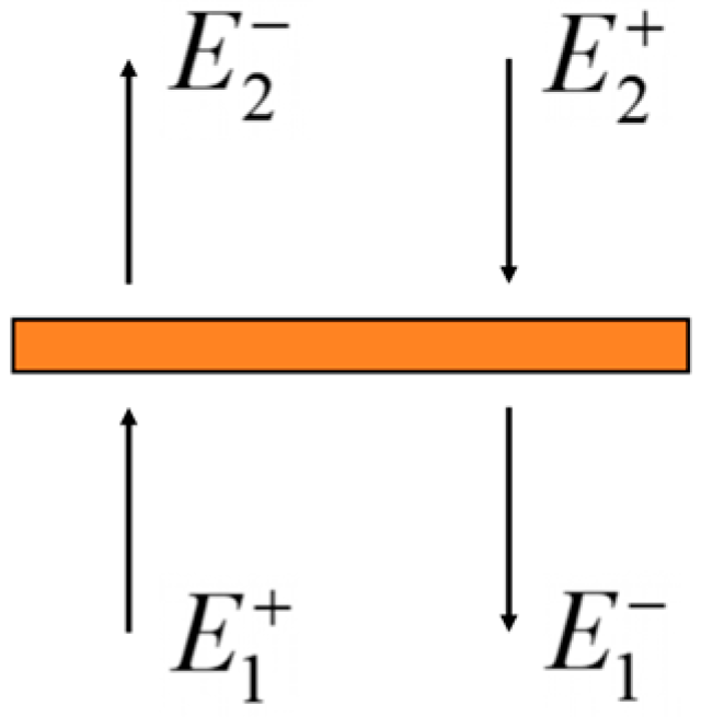
2. Theory and Analysis
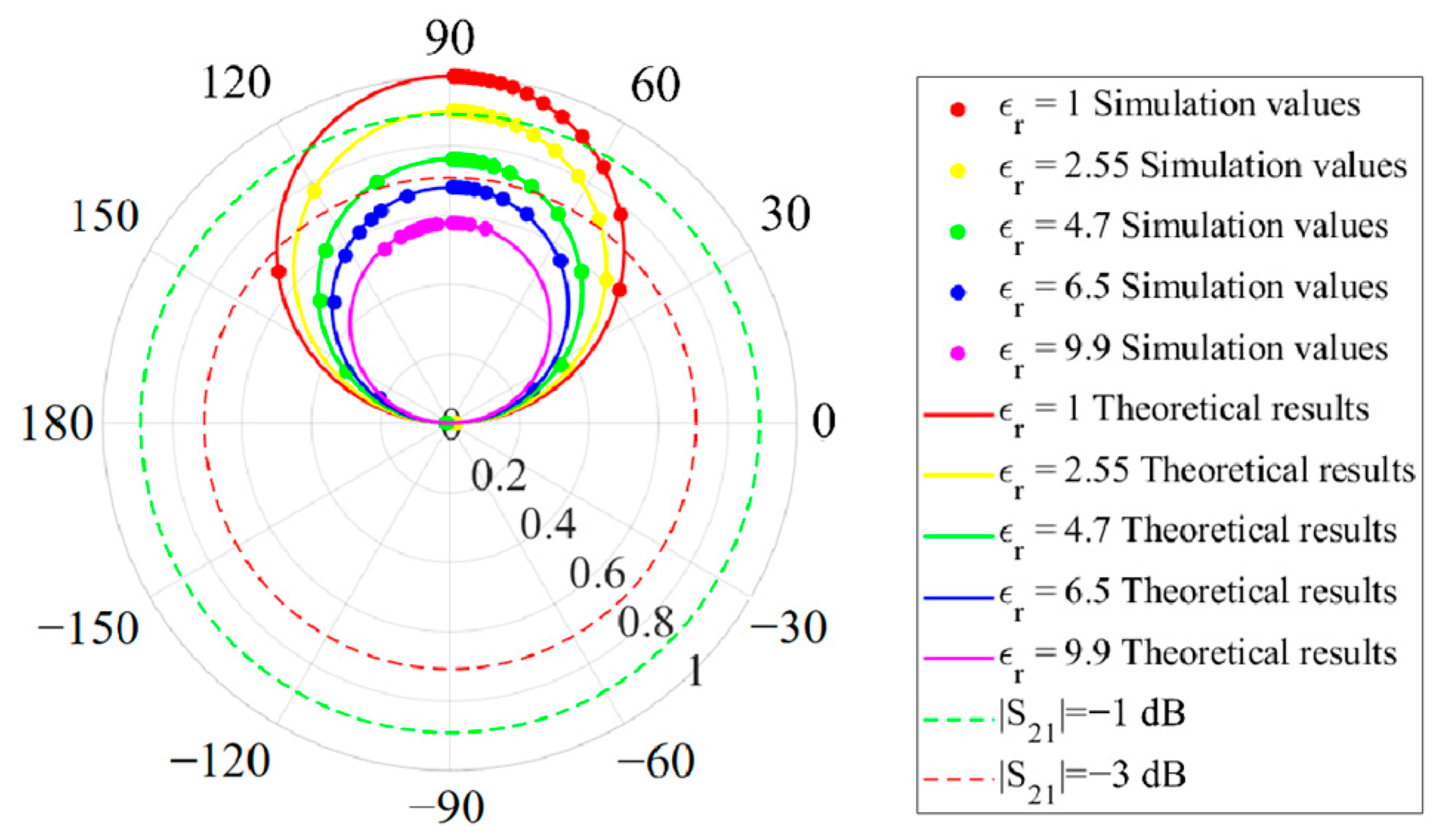
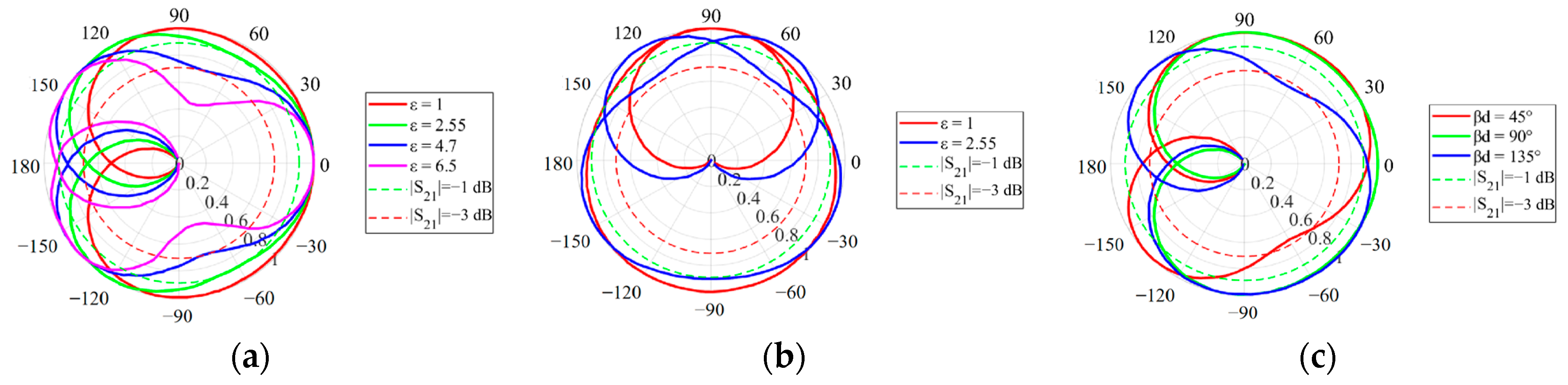
- Dielectric Constant Effect (βd = 90°):
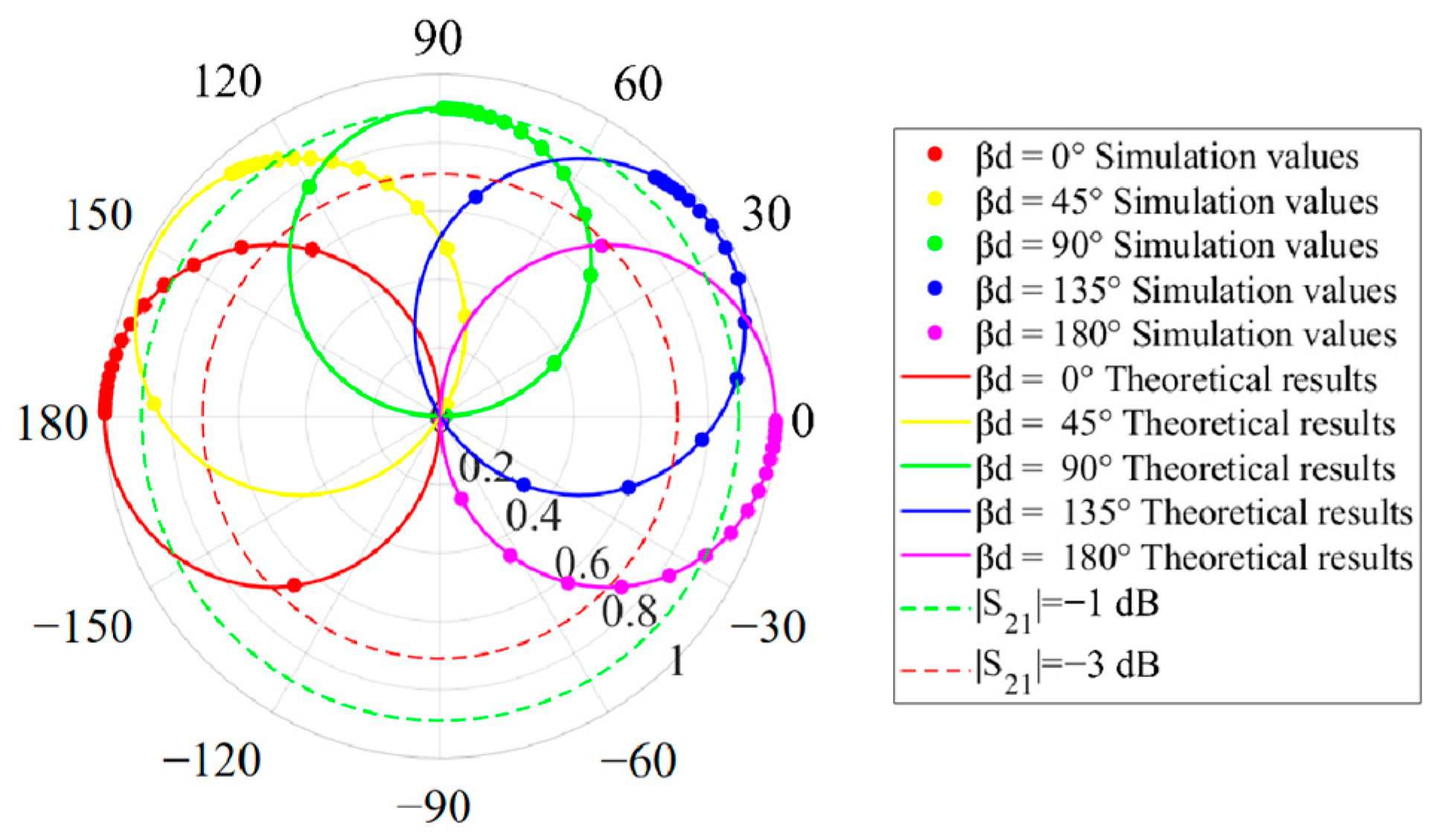
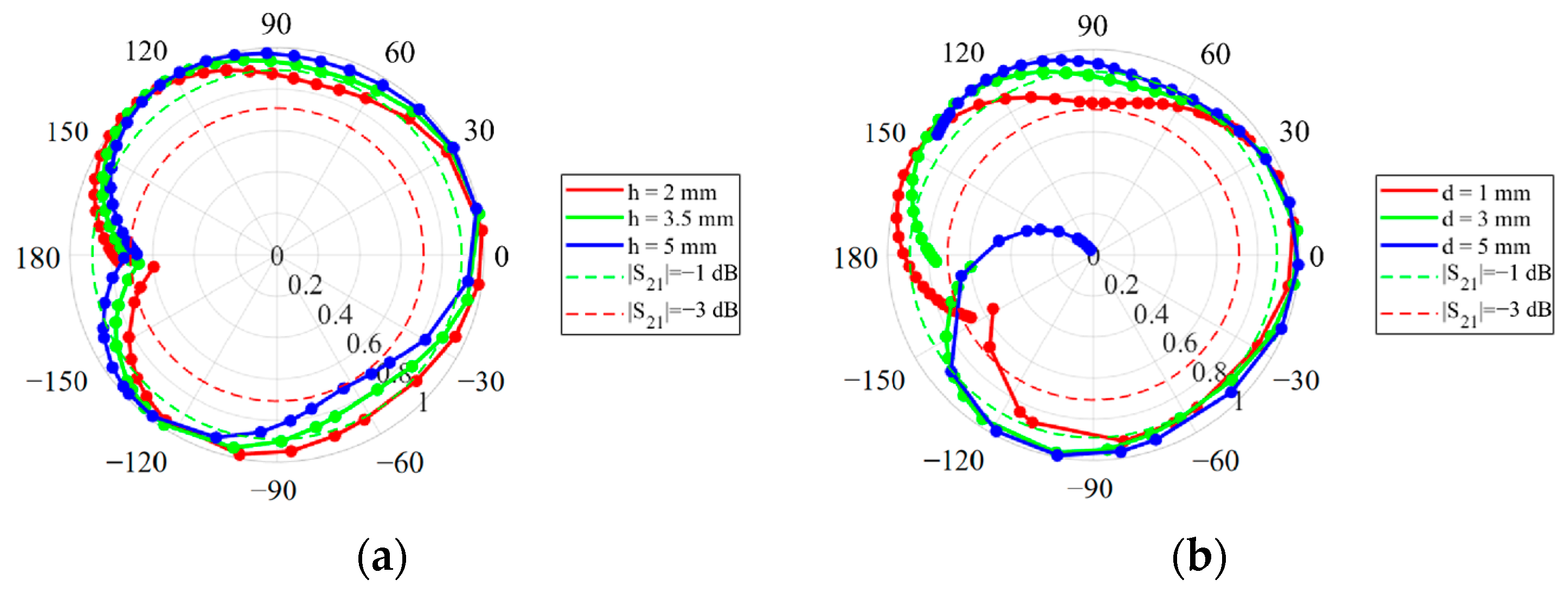
- Electrical Thickness Effect (εr = 2.55):
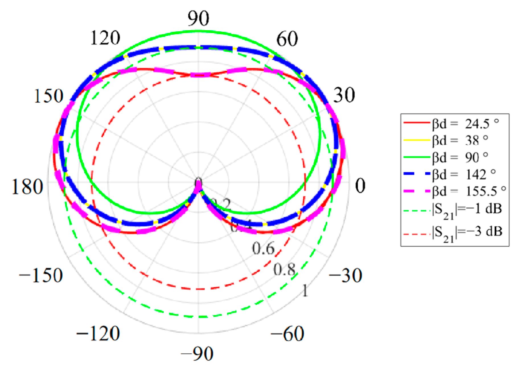
- Dielectric Constant Effect (βd = 90°):
- Electrical Thickness Effect (εr = 1):
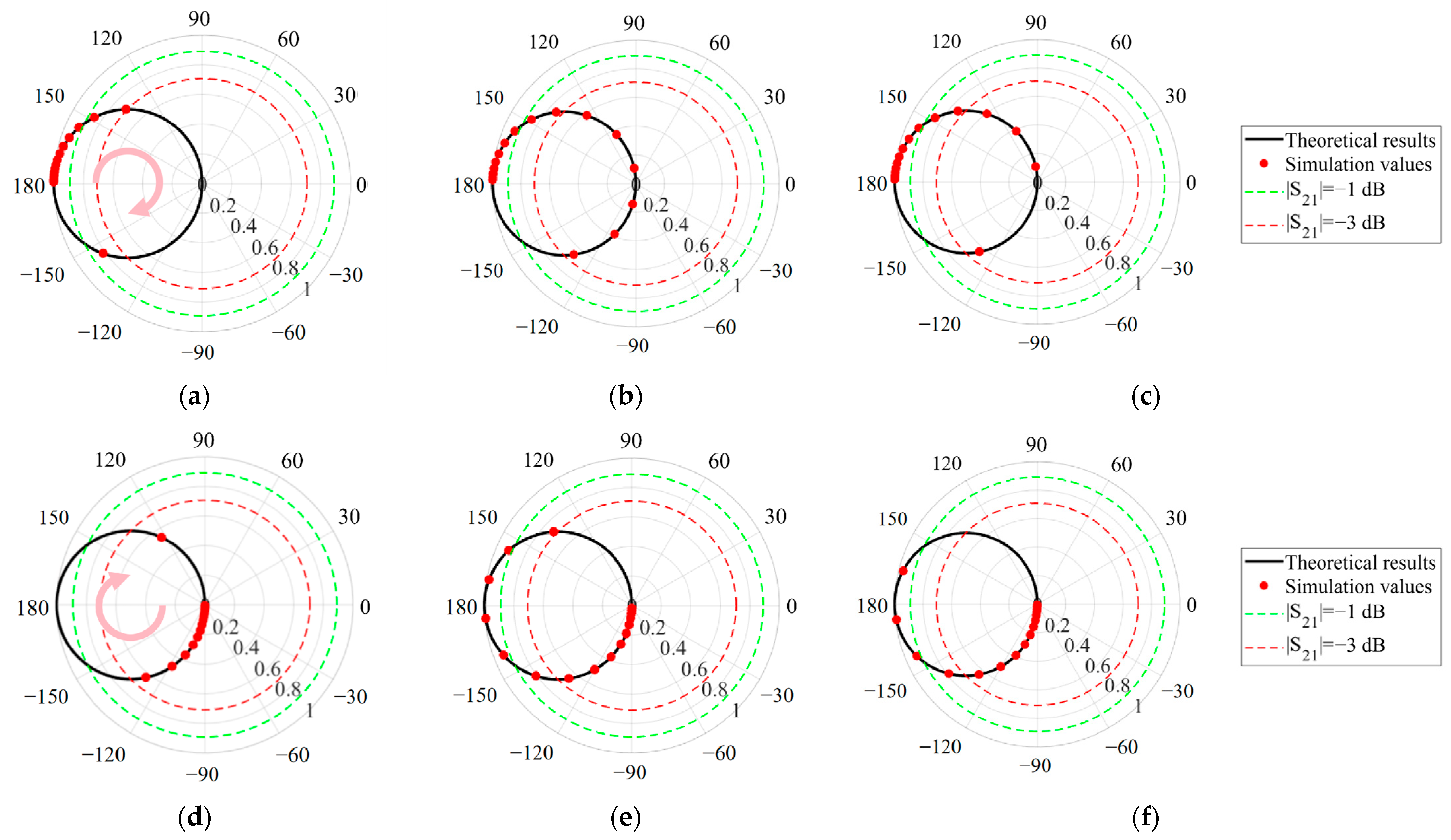
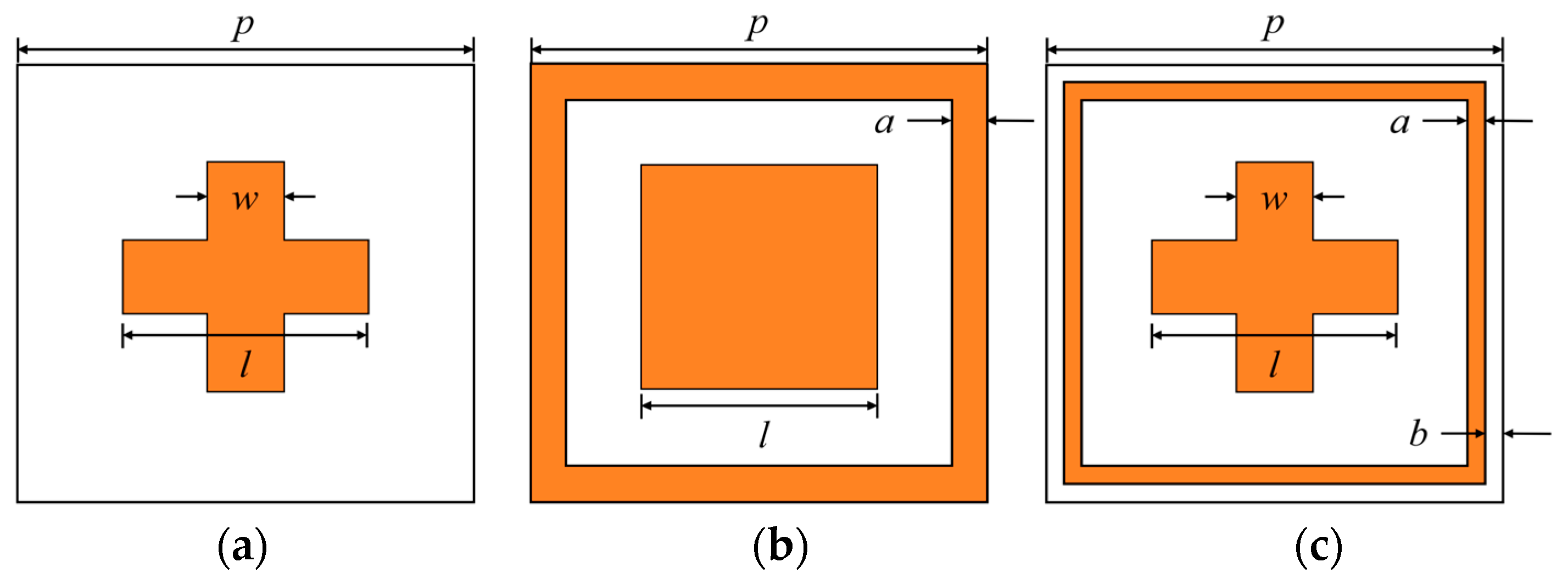
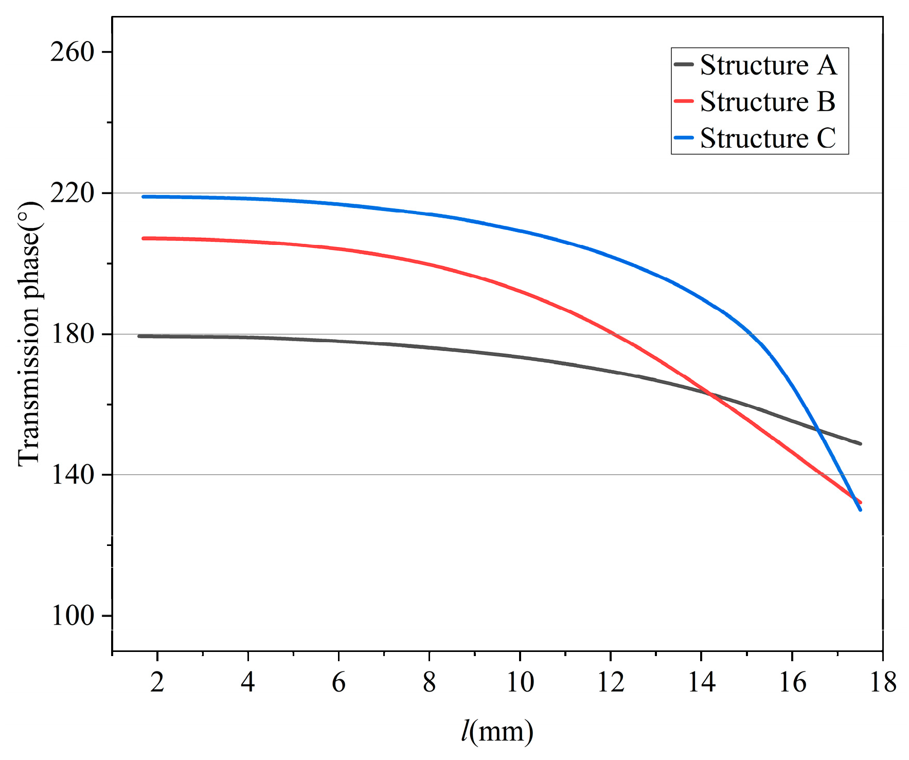
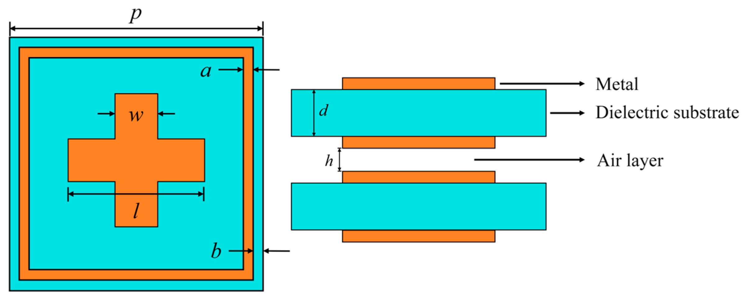
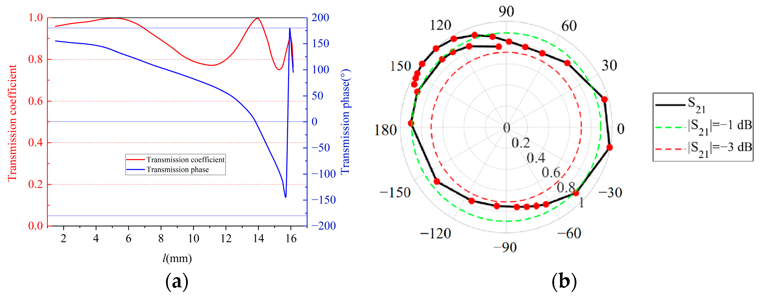
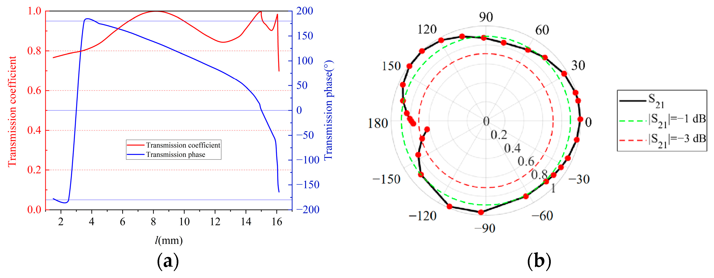
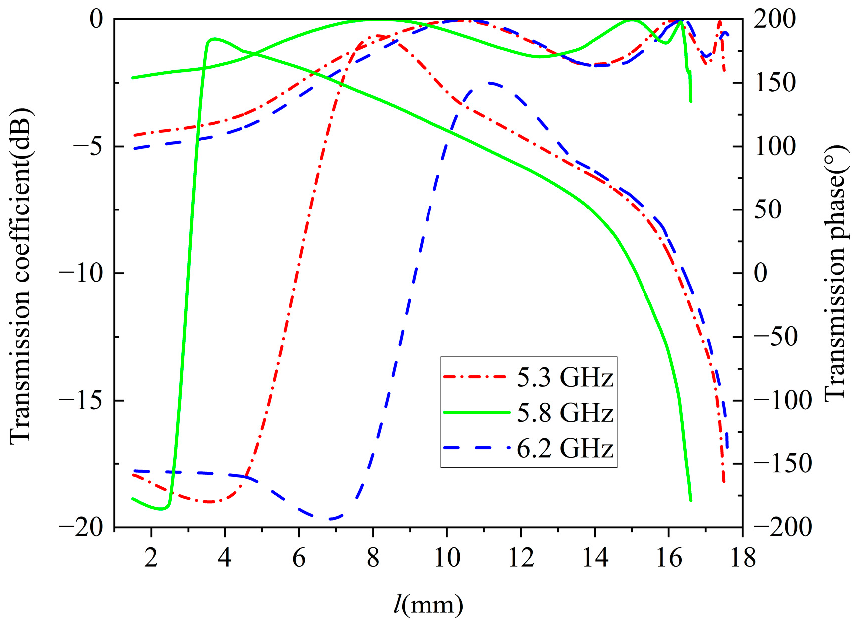
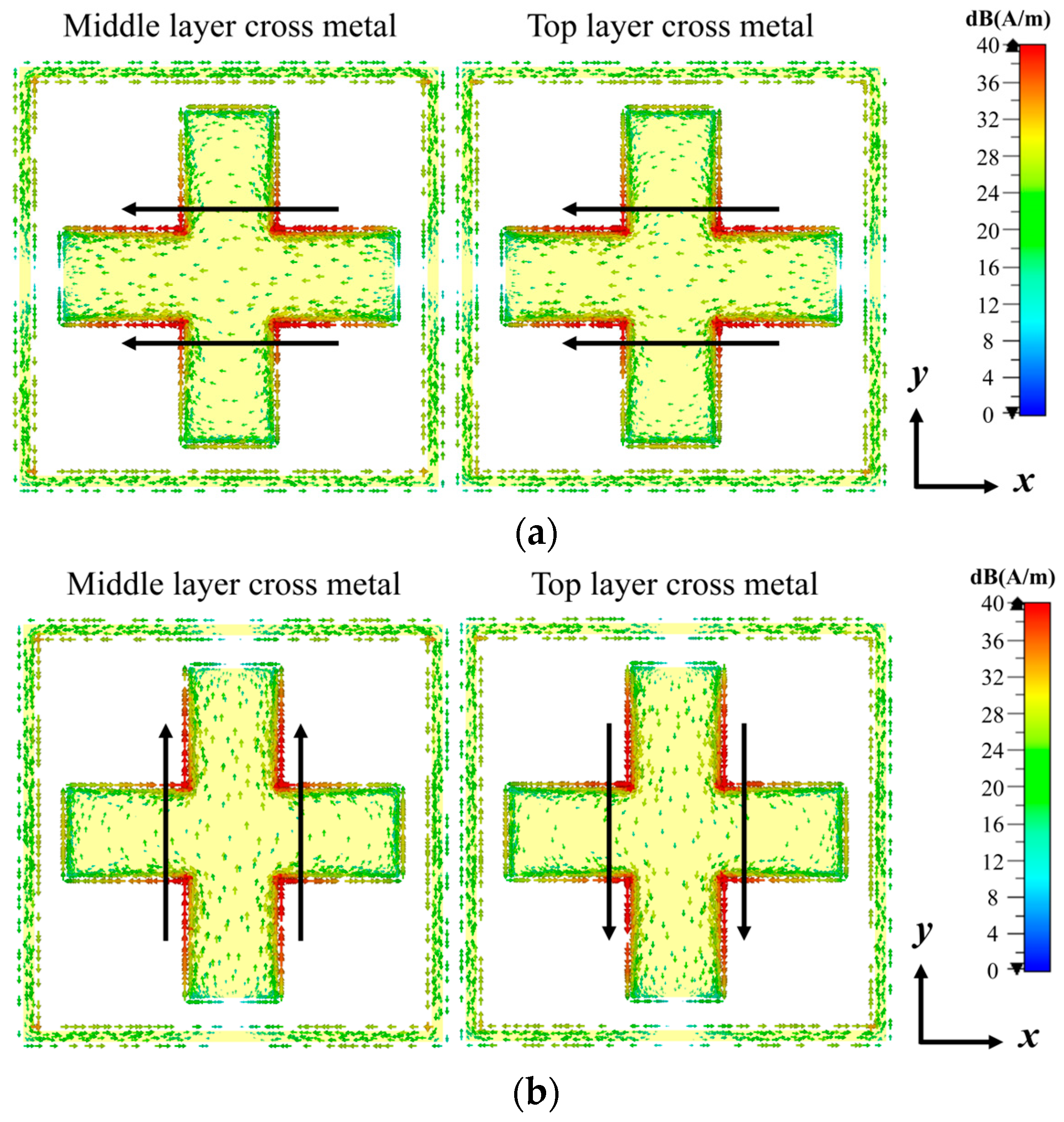
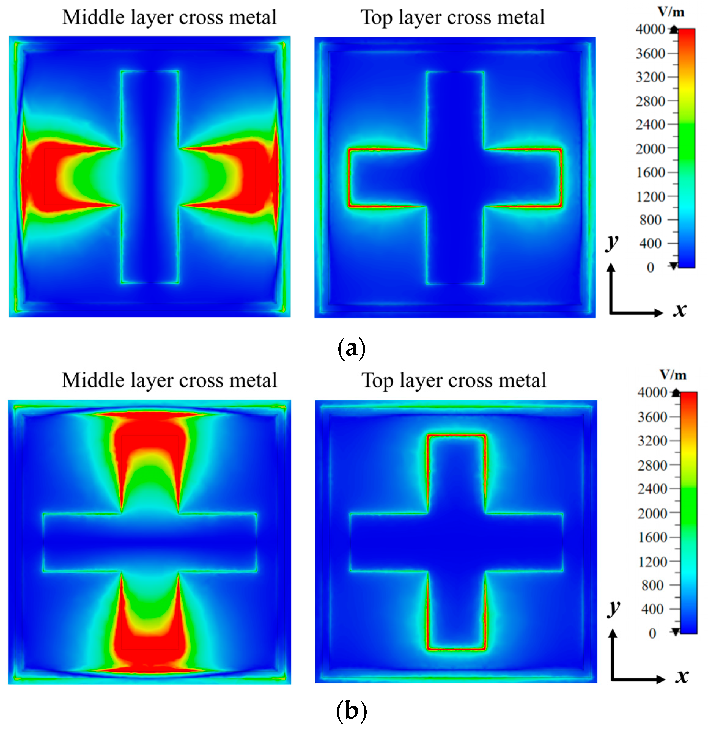
3. Design of Metasurface Units
4. Design Process of Metasurfaces
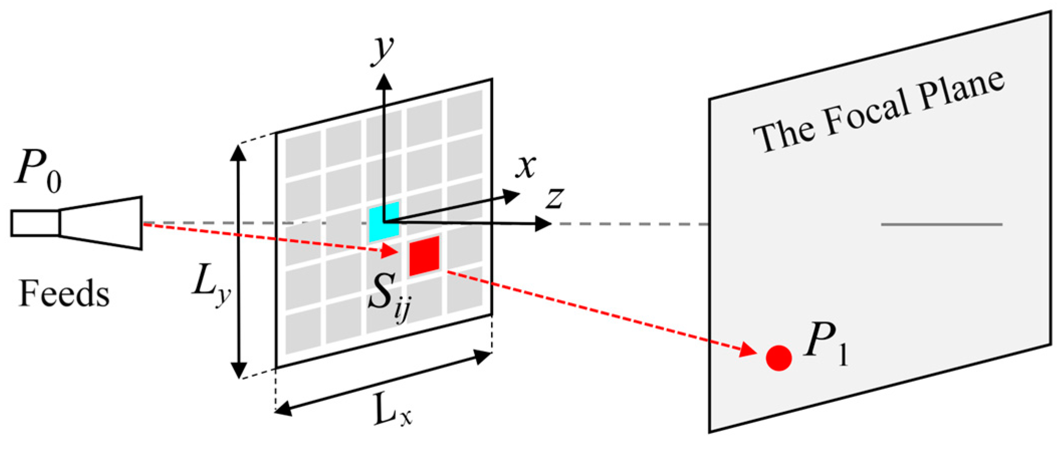
4.1. The Principle and Design Process of Focus
- Define the focusing requirements, such as the focal type and position;
- Compute the transmission phase compensation for each unit based on the phase compensation equation;
- Perform inverse mapping using the transmission coefficient response curve to obtain the corresponding metallic structure dimensions;
- Construct and simulate the metasurface array model to verify the design performance;
- Conduct experimental testing to evaluate its practical performance;
- This systematic design approach ensures the efficiency and accuracy of transmissive metasurfaces in focusing applications.
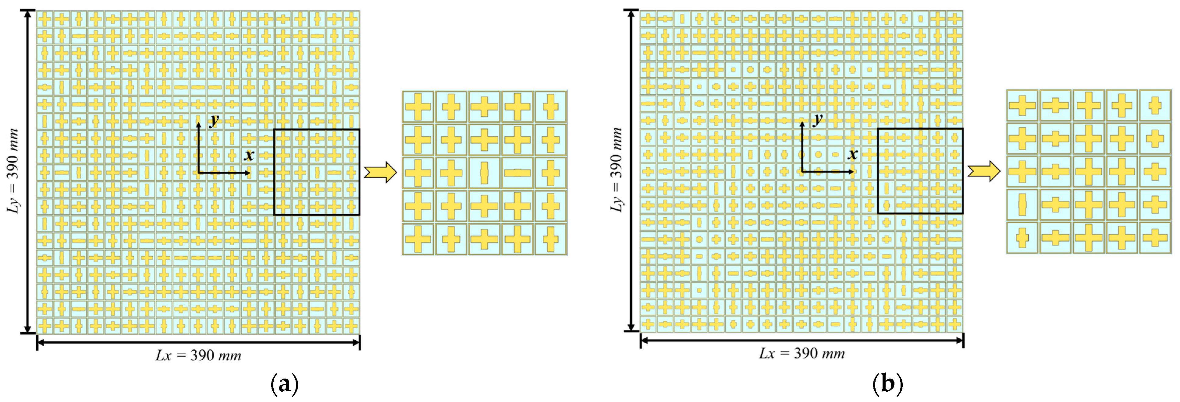
4.2. Design of Transmissive Arrays
- Dual-polarized single-point focusing;
- Dual-polarized dual-point focusing;
- Energy-controlled focusing with a combination of single- and dual-focus modes.
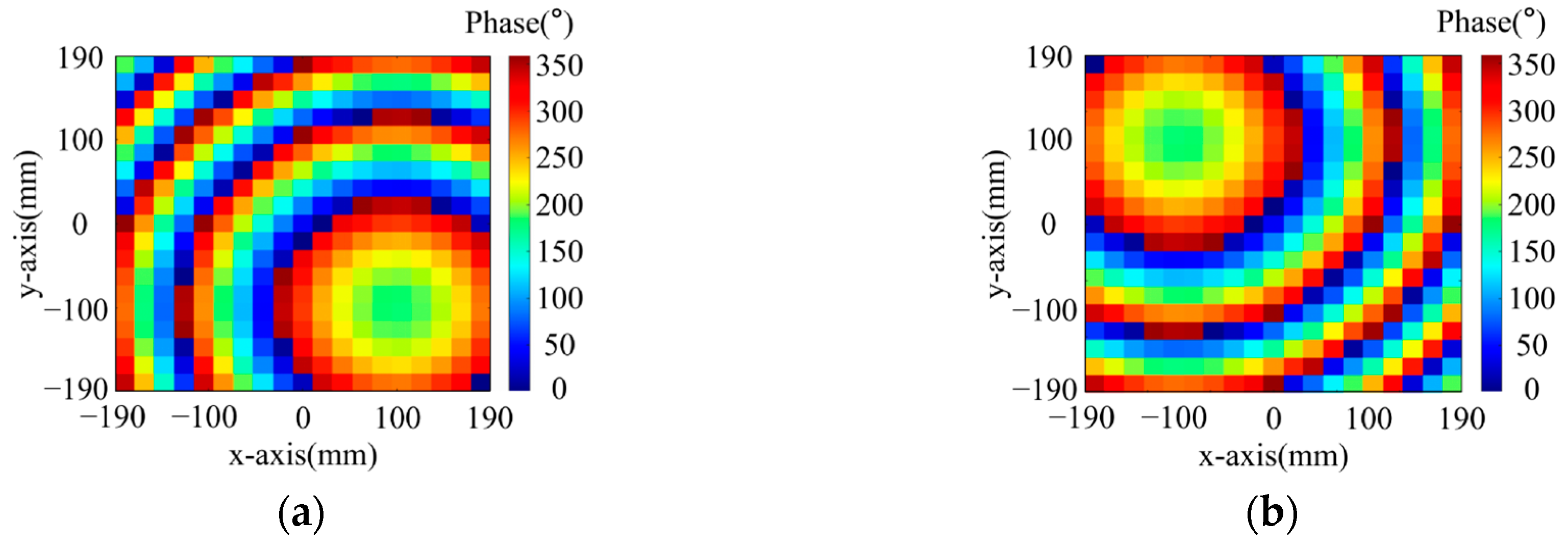
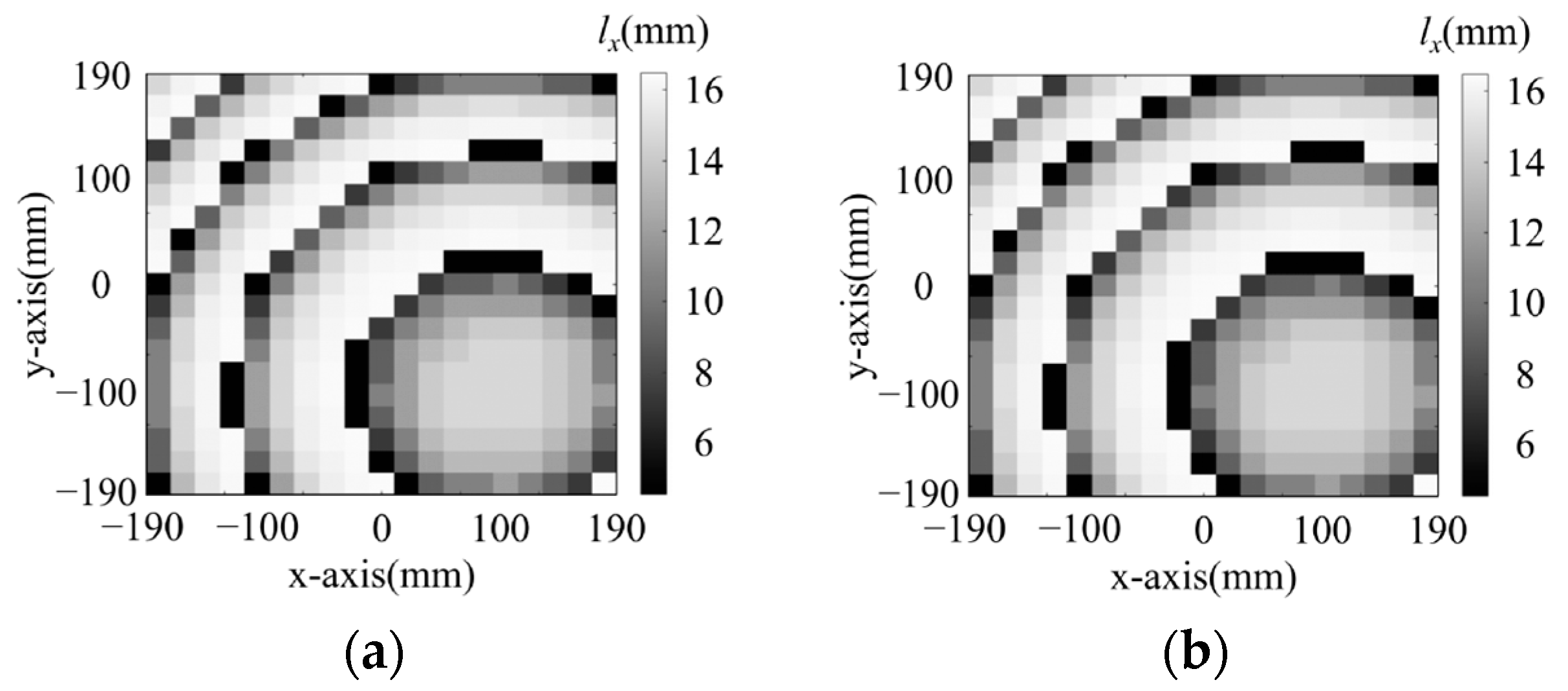
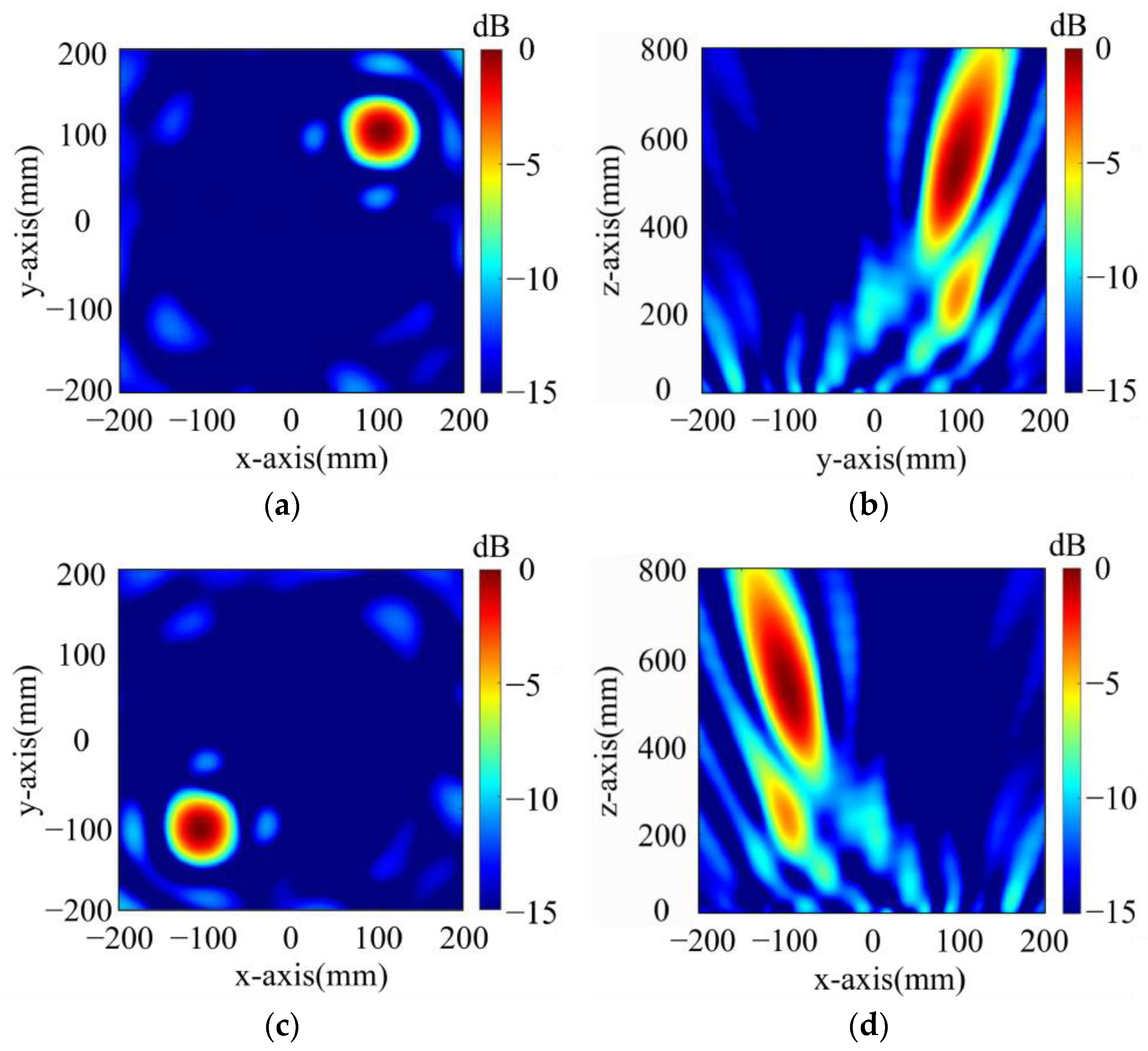
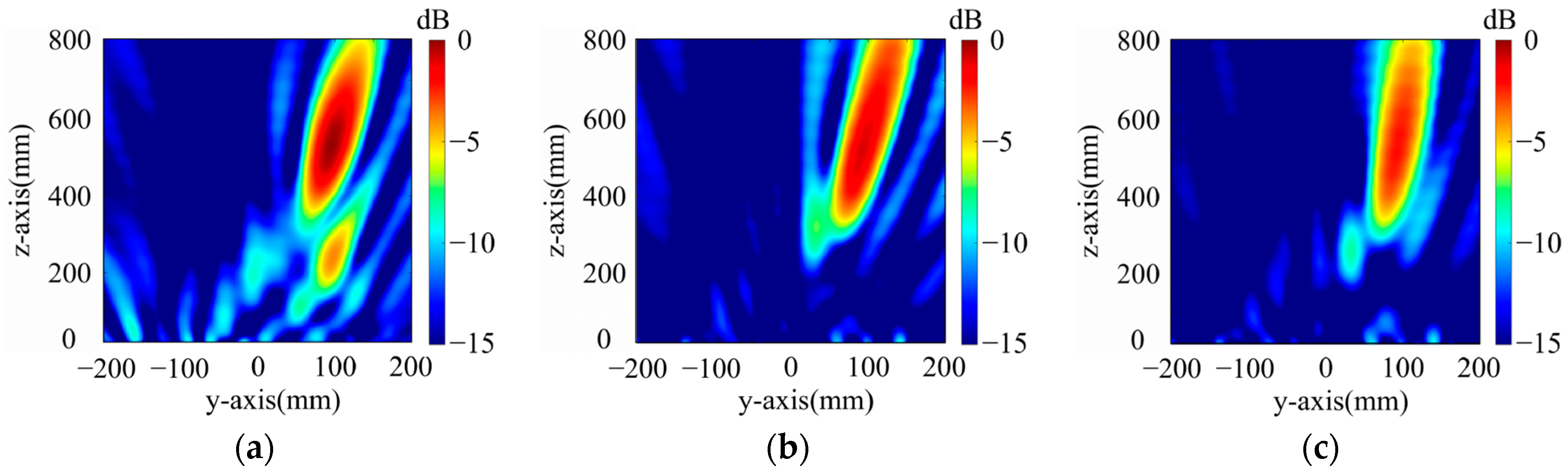
- Dual-Polarized Single-Point Focusing Metasurface
- 2.
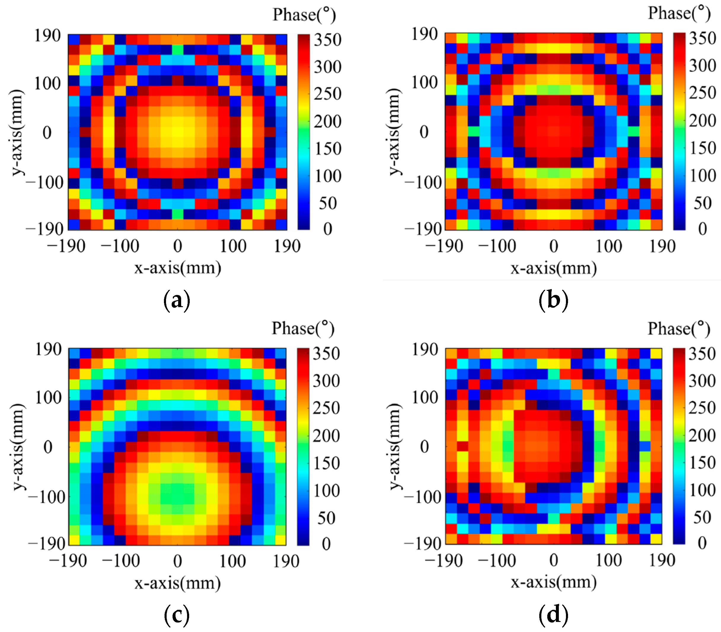
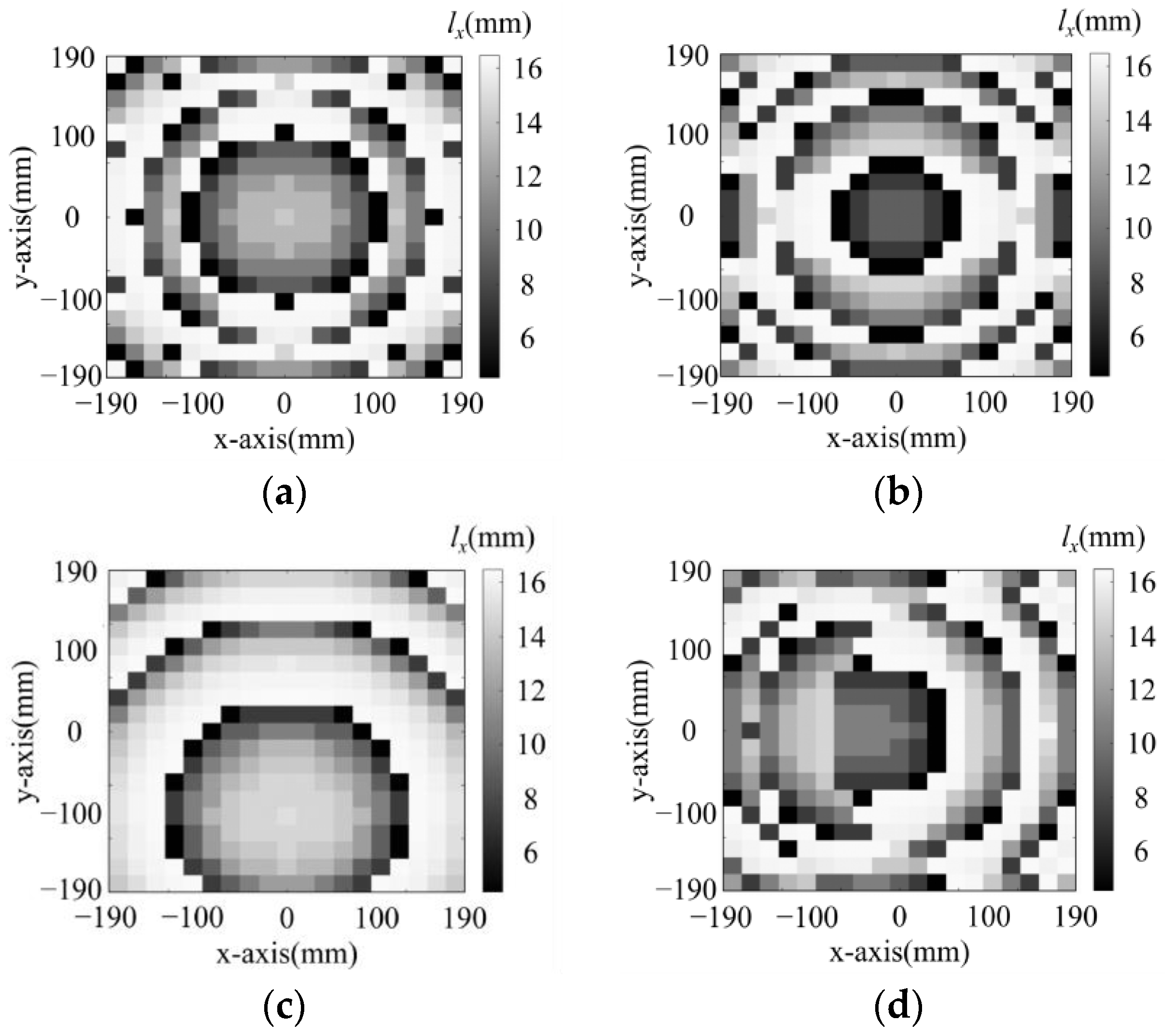
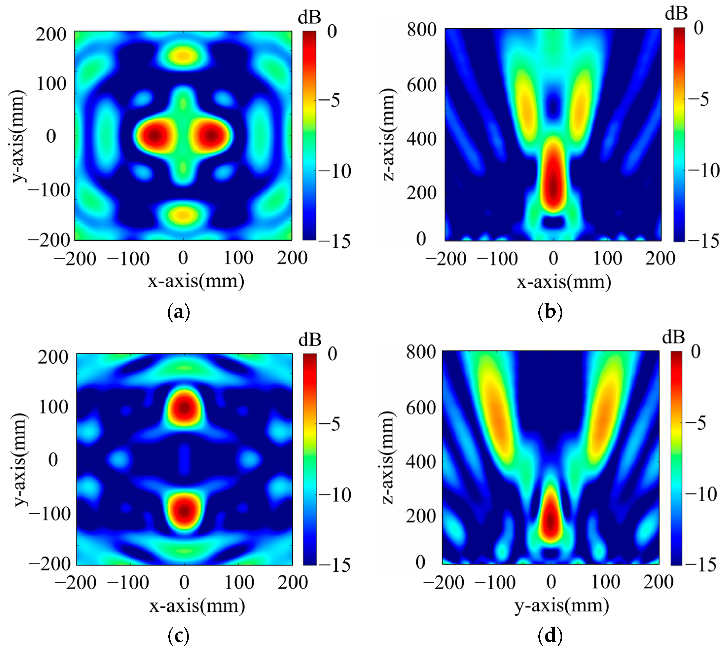
- Dual-Polarized Dual-Point Focusing Metasurface
- For x-polarized excitation, F2x1 (−60 mm, 0 mm, 560 mm), F2x2 (60 mm, 0 mm, 560 mm);
- For y-polarized excitation, F2y1 (0 mm, 100 mm, 560 mm), F2y2 (0 mm, −100 mm, 560 mm).
- 3.
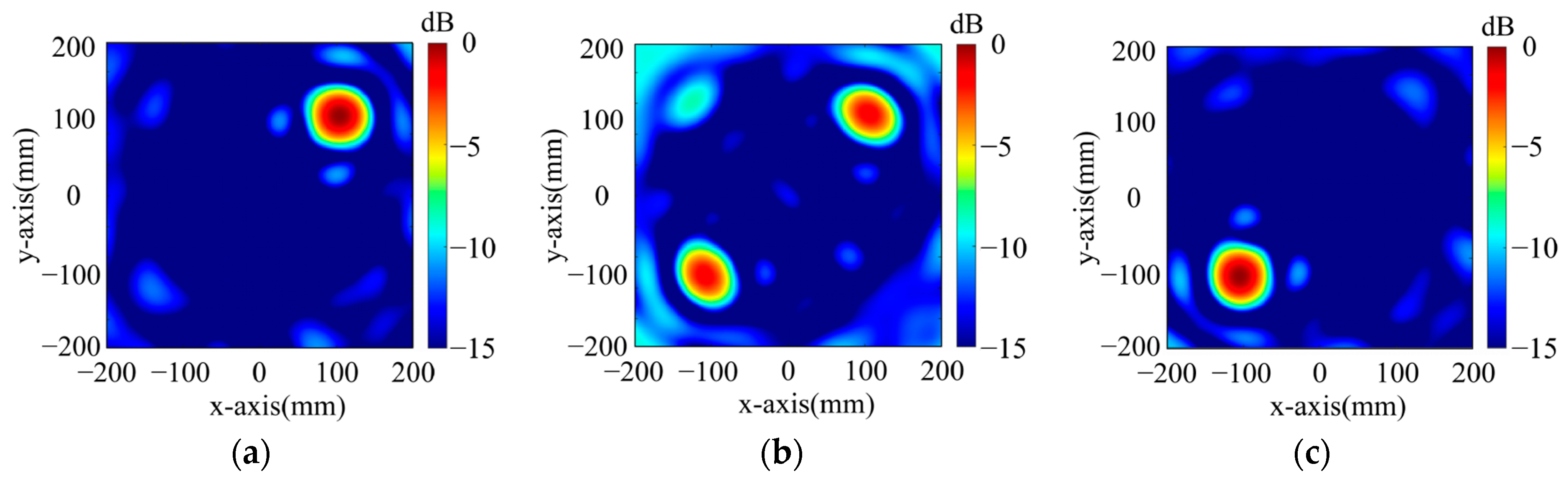
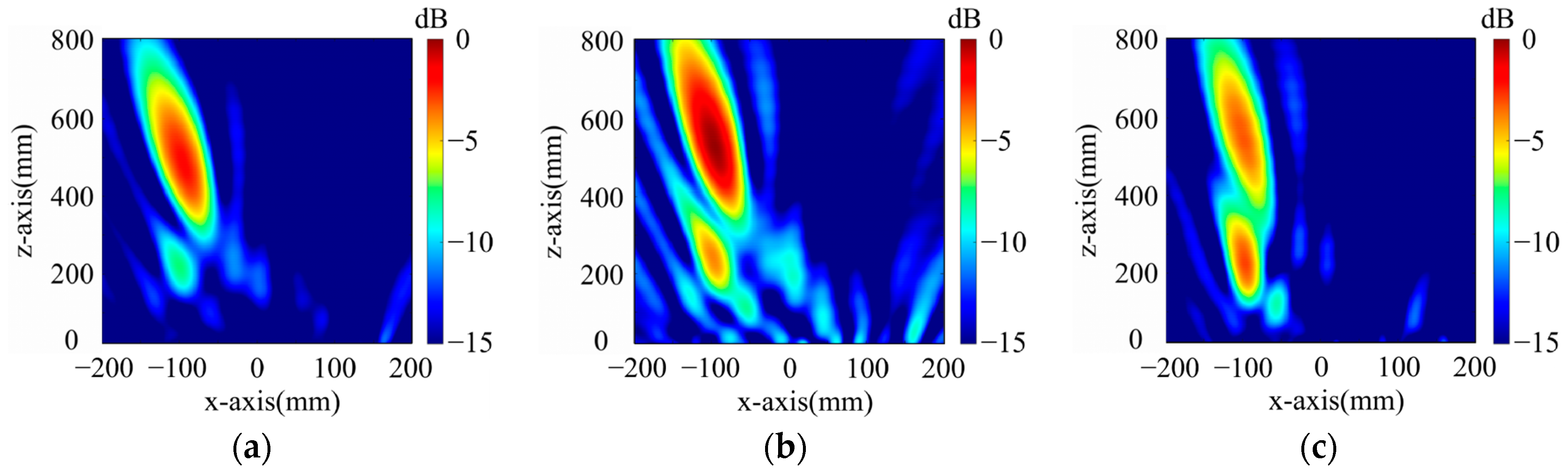
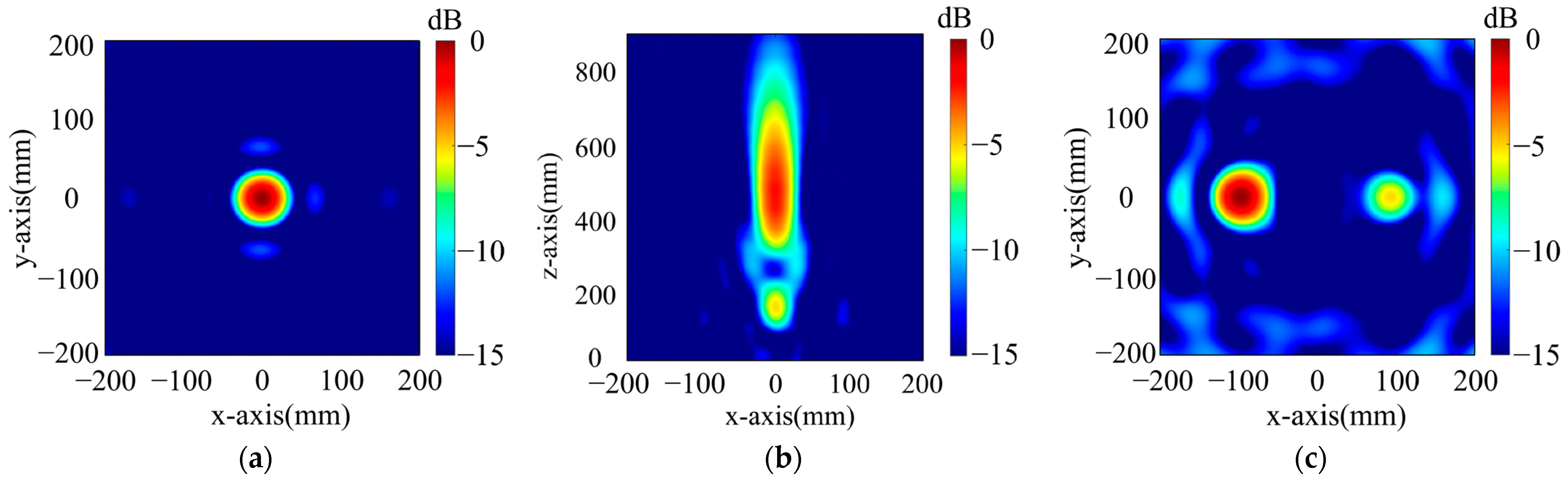
- Energy-Controlled Focused Metasurfaces with Single- and Dual-Focus Modes.
- For x-polarized excitation, F3x (0 mm, 0 mm, 560 mm);
- For y-polarized excitation, F3y1 (−100 mm, 0 mm, 560 mm), F3y2 (100 mm, 0 mm, 560 mm).
5. Simulation Results
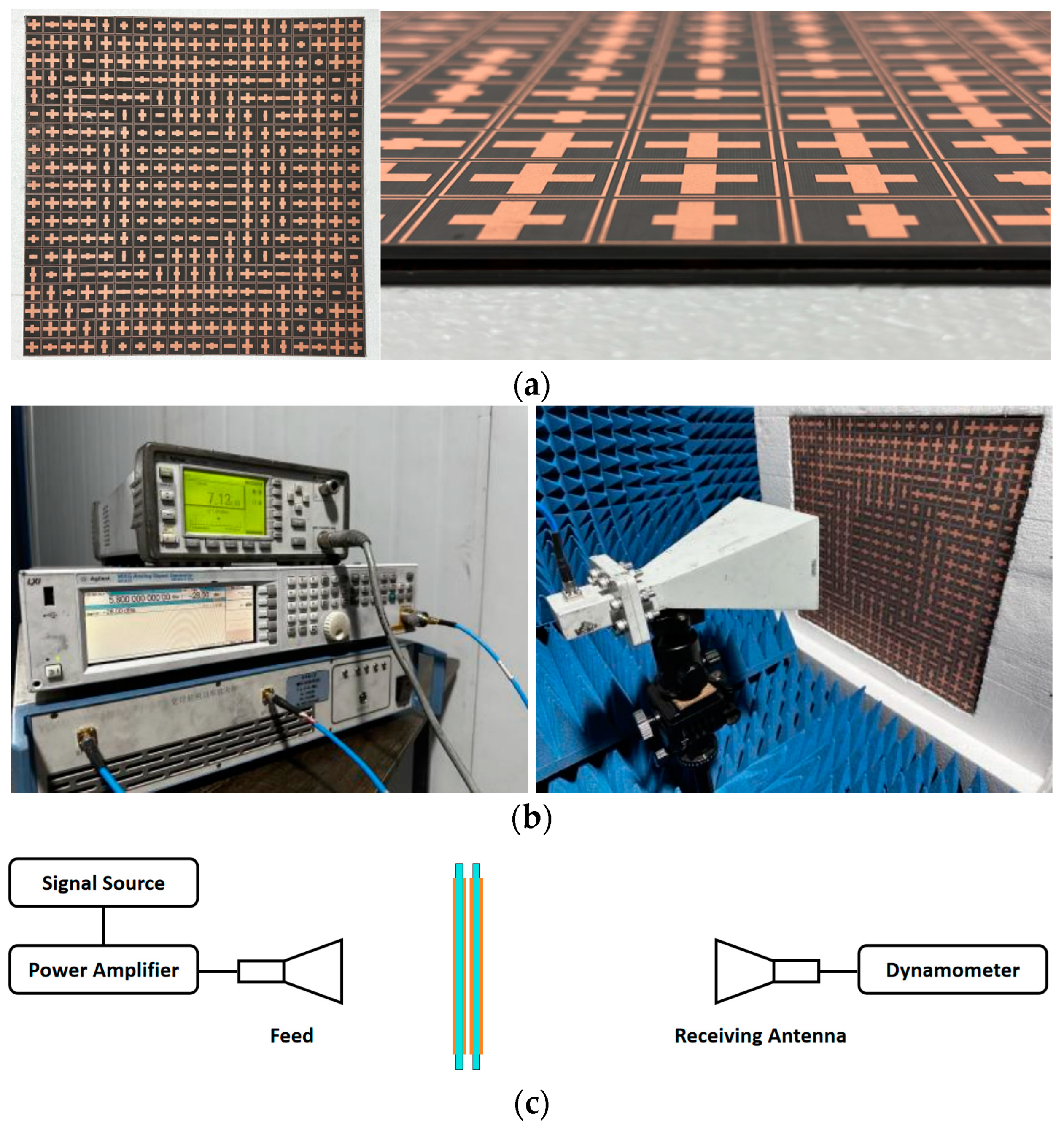
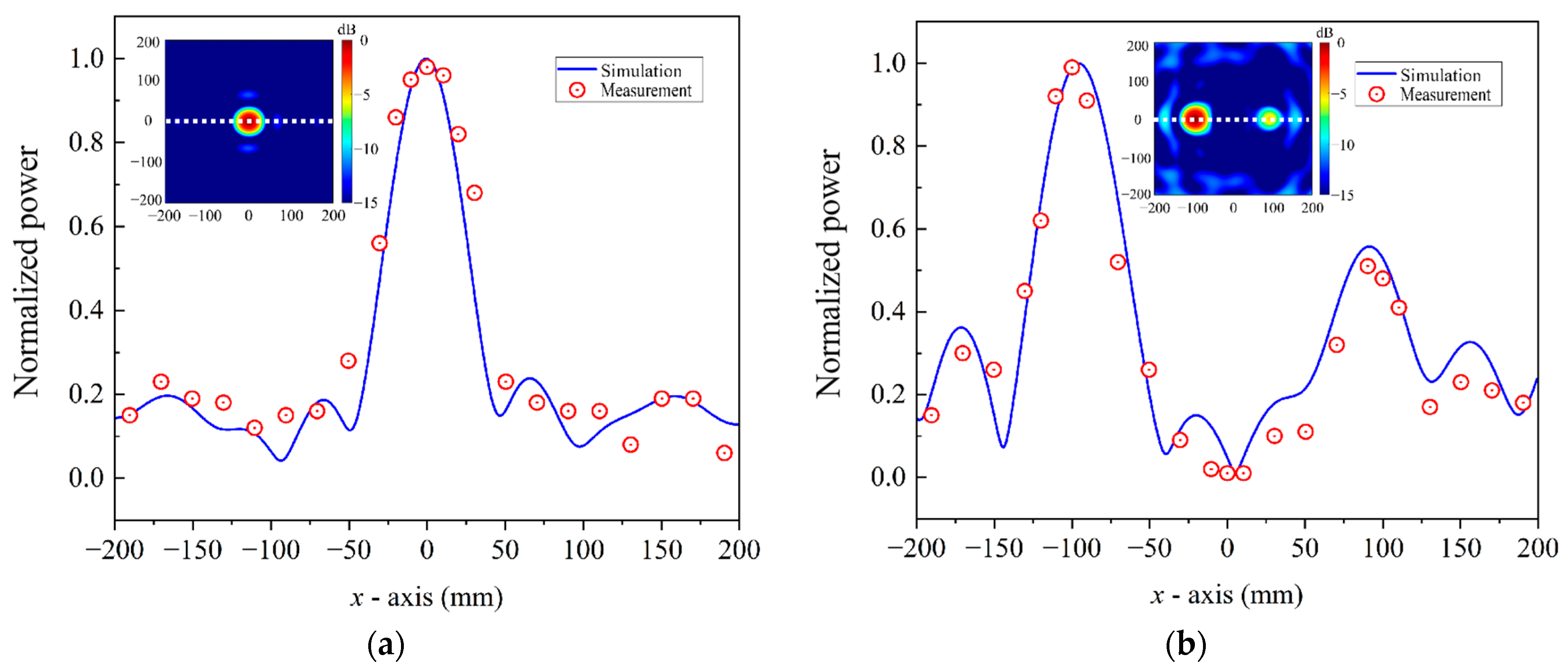
6. Experimental Validation
7. Discussion
Author Contributions
Funding
Data Availability Statement
Conflicts of Interest
References
- Mobashsher, A.T.; Abbosh, A.M. Performance of directional and omnidirectional antennas in wideband head imaging. IEEE Antennas Wirel. Propag. Lett. 2016, 15, 1618–1621. [Google Scholar] [CrossRef]
- Sharma, A.; Zuazola, I.J.G.; Batchelor, J.C.; Perallos, A. Dual purpose near-and far-field UHF RFID coil antenna with non-uniformly distributed-turns. IEEE Antennas Wirel. Propag. Lett. 2015, 14, 1342–1345. [Google Scholar] [CrossRef]
- Le-Huu, H.; Bui, G.T.; Seo, C. Efficient compact radiative near-field wireless power transfer to miniature biomedical implants. IEEE Antennas Wirel. Propag. Lett. 2023, 22, 2803–2807. [Google Scholar] [CrossRef]
- Gowda, V.R.; Yurduseven, O.; Lipworth, G.; Zupan, T.; Reynolds, M.S.; Smith, D.R. Wireless power transfer in the radiative near field. IEEE Antennas Wirel. Propag. Lett. 2016, 15, 1865–1868. [Google Scholar] [CrossRef]
- Bor, J.; Clauzier, S.; Lafond, O.; Himdi, M. 60 GHz foam-based antenna for near-field focusing. Electron. Lett. 2014, 50, 571–572. [Google Scholar] [CrossRef]
- Liu, S.; Lin, X.; Jia, X.; Ping, P. A near field focused lens antenna for wireless power transmission systems. In Proceedings of the 2018 IEEE Asia-Pacific Conference on Antennas and Propagation (APCAP), Auckland, New Zealand, 5–8 August 2018; pp. 313–315. [Google Scholar]
- Markovich, H.; Filonov, D.; Shishkin, I.; Ginzburg, P. Bifocal Fresnel lens based on the polarization-sensitive metasurface. IEEE Trans. Antennas Propag. 2018, 66, 2650–2654. [Google Scholar] [CrossRef]
- Shan, L.; Geyi, W. Optimal design of focused antenna arrays. IEEE Trans. Antennas Propag. 2014, 62, 5565–5571. [Google Scholar] [CrossRef]
- Chou, H.T.; Lee, M.Y.; Yu, C.T. Subsystem of phased array antennas with adaptive beam steering in the near-field RFID applications. IEEE Antennas Wirel. Propag. Lett. 2015, 14, 1746–1749. [Google Scholar] [CrossRef]
- Li, P.F.; Qu, S.W.; Yang, S.; Liu, Y.A.; Xue, Q. Near-field focused array antenna with frequency-tunable focal distance. IEEE Trans. Antennas Propag. 2018, 66, 3401–3410. [Google Scholar] [CrossRef]
- Battaglia, G.M.; Bellizzi, G.G.; Morabito, A.F.; Sorbello, G.; Isernia, T. A general effective approach to the synthesis of shaped beams for arbitrary fixed-geometry arrays. J. Electromagn. Waves Appl. 2019, 33, 2404–2422. [Google Scholar] [CrossRef]
- Battaglia, G.M.; Isernia, T.; Palmeri, R.; Maisto, M.A.; Solimene, R.; Morabito, A.F. Near-Field Synthesis of 1-D Shaped Patterns through Spectral Factorization and Minimally-Redundant Array-Like Representations. IEEE Trans. Antennas Propag. 2025. [Google Scholar] [CrossRef]
- Chou, H.T.; Hung, T.M.; Wang, N.N.; Chou, H.H.; Tung, C.; Nepa, P. Design of a near-field focused reflectarray antenna for 2.4 GHz RFID reader applications. IEEE Trans. Antennas Propag. 2010, 59, 1013–1018. [Google Scholar] [CrossRef]
- Ma, W.; Jia, D.; Yu, X.; Feng, Y.; Zhao, Y. Reflective gradient metasurfaces for polarization-independent light focusing at normal or oblique incidence. Appl. Phys. Lett. 2016, 108, 071111. [Google Scholar] [CrossRef]
- Hou, H.S.; Wang, G.M.; Li, H.P.; Guo, W.L.; Li, T.J.; Cai, T. Single-layer broadband planar antenna using ultrathin high-efficiency focusing metasurfaces. Chin. Phys. B 2017, 26, 057701. [Google Scholar] [CrossRef]
- Yu, S.; Liu, H.; Li, L. Design of near-field focused metasurface for high-efficient wireless power transfer with multifocus characteristics. IEEE Trans. Ind. Electron. 2018, 66, 3993–4002. [Google Scholar] [CrossRef]
- Li, T.; Liang, J. Single-layer transparent focusing metasurface and its application to high gain circularly polarized lens antenna. In Proceedings of the 2016 IEEE International Workshop on Electromagnetics: Applications and Student Innovation Competition (iWEM), Nanjing, China, 16–18 May 2016; pp. 1–3. [Google Scholar]
- Li, H.; Wang, G.; Liang, J.; Gao, X.; Hou, H.; Jia, X. Single-layer focusing gradient metasurface for ultrathin planar lens antenna application. IEEE Trans. Antennas Propag. 2016, 65, 1452–1457. [Google Scholar] [CrossRef]
- Cai, T.; Wang, G.; Tang, S.; Xu, H.; Duan, J.; Guo, H.; Guan, F.; Sun, S.; He, Q.; Zhou, L. High-efficiency and full-space manipulation of electromagnetic wave fronts with metasurfaces. Phys. Rev. Appl. 2017, 8, 034033. [Google Scholar] [CrossRef]
- Luo, J.; Yang, F.; Xu, S.; Li, M.; Gu, S. A high gain broadband transmitarray antenna using dual-resonant E-shaped element. Microw. Opt. Technol. Lett. 2018, 60, 1531–1536. [Google Scholar] [CrossRef]


| Unit Structure (βd = 90°) | Dielectric Constant εr | Transmission Phase Range (°) | |
|---|---|---|---|
| |S21| > −1 dB | |S21| > −3 dB | ||
| Single-metal-layer unit | 1 | 54 | 90 |
| 2.55 | 13 | 76 | |
| 4.7 | 44 | ||
| 6.5 | |||
| 9.9 | |||
| Bimetallic-layer unit | 1 | 128 | 180 |
| 2.55 | 162 | 210 | |
| 4.7 | 225 | ||
| 6.5 | |||
| Three-metal-layer unit | 1 | 264 | 316 |
| 2.55 | 310 | 360 | |
| 4.7 | 360 | ||
| 6.5 | |||
| Four-metal-layer unit | 1 | 360 | 360 |
| 2.55 | 336 | 360 | |
| Unit Structure | Electrical Thickness βd (°) | Transmission Phase Range (°) | |
|---|---|---|---|
| |S21| > −1 dB | |S21| > −3 dB | ||
| Single-metal-layer unit (εr = 2.55) | 90 | 0 | 80 |
| 90 ± 45 | 50 | 87 | |
| 90 ± 90 | 54 | 90 | |
| Bimetallic-layer unit (εr = 2.55) | 90 | 168 | 210 |
| 90 ± 48 | 122 | 228 | |
| Bimetallic-layer unit (εr = 1) | 90 | 125 | 180 |
| 90 ± 52 | 172 | 210 | |
| 90 ± 65.5 | 120 | 225 | |
| Three-metal-layer unit (εr = 1) | 90 | 266 | 318 |
| 90 ± 45 | 210 | 320 | |
| Structure A | Structure B | Structure C | |
|---|---|---|---|
| p (unit: mm) | 20 | 20 | 20 |
| w (unit: mm) | 4 | 4 | |
| a (unit: mm) | 0.5 | 0.5 | |
| b (unit: mm) | 0.5 | ||
| l (unit: mm) | 1.5~20 | 1.5~19 | 1.5~17.5 |
Disclaimer/Publisher’s Note: The statements, opinions and data contained in all publications are solely those of the individual author(s) and contributor(s) and not of MDPI and/or the editor(s). MDPI and/or the editor(s) disclaim responsibility for any injury to people or property resulting from any ideas, methods, instructions or products referred to in the content. |
© 2025 by the authors. Licensee MDPI, Basel, Switzerland. This article is an open access article distributed under the terms and conditions of the Creative Commons Attribution (CC BY) license (https://creativecommons.org/licenses/by/4.0/).
Share and Cite
Guo, C.; Li, J. Polarization-Multiplexed Transmissive Metasurfaces for Multifunctional Focusing at 5.8 GHz. Electronics 2025, 14, 1774. https://doi.org/10.3390/electronics14091774
Guo C, Li J. Polarization-Multiplexed Transmissive Metasurfaces for Multifunctional Focusing at 5.8 GHz. Electronics. 2025; 14(9):1774. https://doi.org/10.3390/electronics14091774
Chicago/Turabian StyleGuo, Chenjie, and Jian Li. 2025. "Polarization-Multiplexed Transmissive Metasurfaces for Multifunctional Focusing at 5.8 GHz" Electronics 14, no. 9: 1774. https://doi.org/10.3390/electronics14091774
APA StyleGuo, C., & Li, J. (2025). Polarization-Multiplexed Transmissive Metasurfaces for Multifunctional Focusing at 5.8 GHz. Electronics, 14(9), 1774. https://doi.org/10.3390/electronics14091774