Article

Investigation of a 220 GHz Traveling-Wave Tube Based upon a Flat-Roofed Sine Waveguide with a Coupling Structure

1
China Electronic Product Reliability and Environmental Testing Research Institute, Guangzhou 511370, China
2
Guangzhou Huali Science and Technology Vocational College, Guangzhou 511325, China
*
Authors to whom correspondence should be addressed.
Electronics 2025, 14(9), 1756; https://doi.org/10.3390/electronics14091756
Submission received: 23 February 2025 / Revised: 24 March 2025 / Accepted: 26 March 2025 / Published: 25 April 2025
(This article belongs to the Special Issue Vacuum Electronics: From Micro to Nano)

Abstract

:
This paper presents the design and investigation of a two-stage flat-roofed sine waveguide (SWG) traveling-wave tube (TWT) incorporating a novel coupling structure. Initially, the slow-wave structure (SWS) of a 220 GHz flat-roofed SWG was optimized, and the output performance of the corresponding TWT was thoroughly analyzed. Subsequently, a specialized coupling structure was designed and fabricated, with the experimental results demonstrating an excellent agreement with the simulation predictions. The coupling structure exhibits low reflection and is easily manufacturable, making it highly suitable for energy coupling in two-stage TWTs. Finally, a two-stage TWT, integrating both the optimized flat-roofed SWG structure and the coupling structure, was developed and characterized. Under operating conditions of a 20.8 kV beam voltage, 150 mA current, and 150 mW input power, the proposed TWT achieved remarkable performance metrics: a maximum output power of 160 W within the frequency range 210–230 GHz and a 3 dB bandwidth exceeding 20 GHz. This research provides a valuable reference solution for the realization of high-power, broadband terahertz radiation sources, contributing significantly to the advancement of terahertz vacuum electronic devices.

1. Introduction

Terahertz technology has been applied in various fields, such as non-destructive testing, high-speed communication and information technology, biomedical imaging, among others [1,2,3,4,5]. Traveling-wave tubes (TWTs), as a type of broadband terahertz source, have recently garnered significant attention [6,7,8,9]. However, as TWTs operate in the sub-millimeter wave and even terahertz bands, the slow-wave structure (SWS), which is a core component of TWTs, experiences a drastic reduction in size, increased transmission loss, and decreased power capacity, severely limiting the output performance of TWTs. Therefore, enhancing the output power, gain, efficiency, and other key parameters of terahertz TWTs has become a focal point of the industry research.
Enhancing the output performance of terahertz TWTs primarily involves several critical considerations. First and foremost, the selection of the SWS, which serves as the core component of a TWT, is of paramount importance. Operating in the terahertz band necessitates the careful consideration of transmission losses. Currently, commonly used structures include folded waveguides [10] and staggered double-vane structures [11,12], both of which are suitable for the terahertz band. However, all-metal SWSs, particularly the sine waveguide (SWG) [13], exhibit lower transmission losses in the terahertz band, making them more suitable for terahertz applications.
Secondly, power synthesis methods or approaches involving multiple electron beam interactions are often employed to improve the output performance of terahertz TWTs [14]. While these methods are effective to some extent, they require a careful consideration of synthesis efficiency. Another approach involves modifying the dimensional parameters at the end of the SWS to achieve phase velocity tapering in the TWT [15]. This allows the electron beam, which has already transferred energy, to continue interacting, thereby further enhancing the output power of the TWT. However, due to the inherent characteristics of TWTs, the power enhancement potential of this method is limited.
The use of overmoded SWSs with multiple electron beams is another method to increase the output power of TWTs [16,17]. By increasing the transverse dimensions of the SWS, the power handling capacity can be improved, and the interaction region between the electron beam and the SWS can be expanded, thereby enhancing the output performance of the TWT. Although the interaction region is increased, operating in higher-order modes results in a reduction in the interaction impedance of the SWS. Consequently, this method is less effective in enhancing TWT performance.
In this article, a two-stage flat-roofed SWG TWT based on a coupling structure is proposed and designed, with simulations and analyses conducted on the transmission and output performance of the two-stage TWT. Firstly, optimization design research is conducted on the flat-roofed SWG SWS operating at 220 GHz, achieving a compromise between the operating bandwidth and interaction impedance. The output performance of a single-stage TWT under different input powers is investigated. Secondly, a coupling structure operating at 220 GHz is proposed and designed, and it is milled using nano-CNC technology. The test results of the coupling structure exhibit an almost identical performance to the simulation results. Finally, two single-stage TWTs are connected through the coupling structure to form a two-stage TWT, with the output of the first TWT serving as the input of the second TWT. The output performance of the two-stage TWT operating at 220 GHz is simulated, and the amplitude–frequency characteristic curve of the two-stage TWT is presented.

2. Flat-Roofed SWG TWT

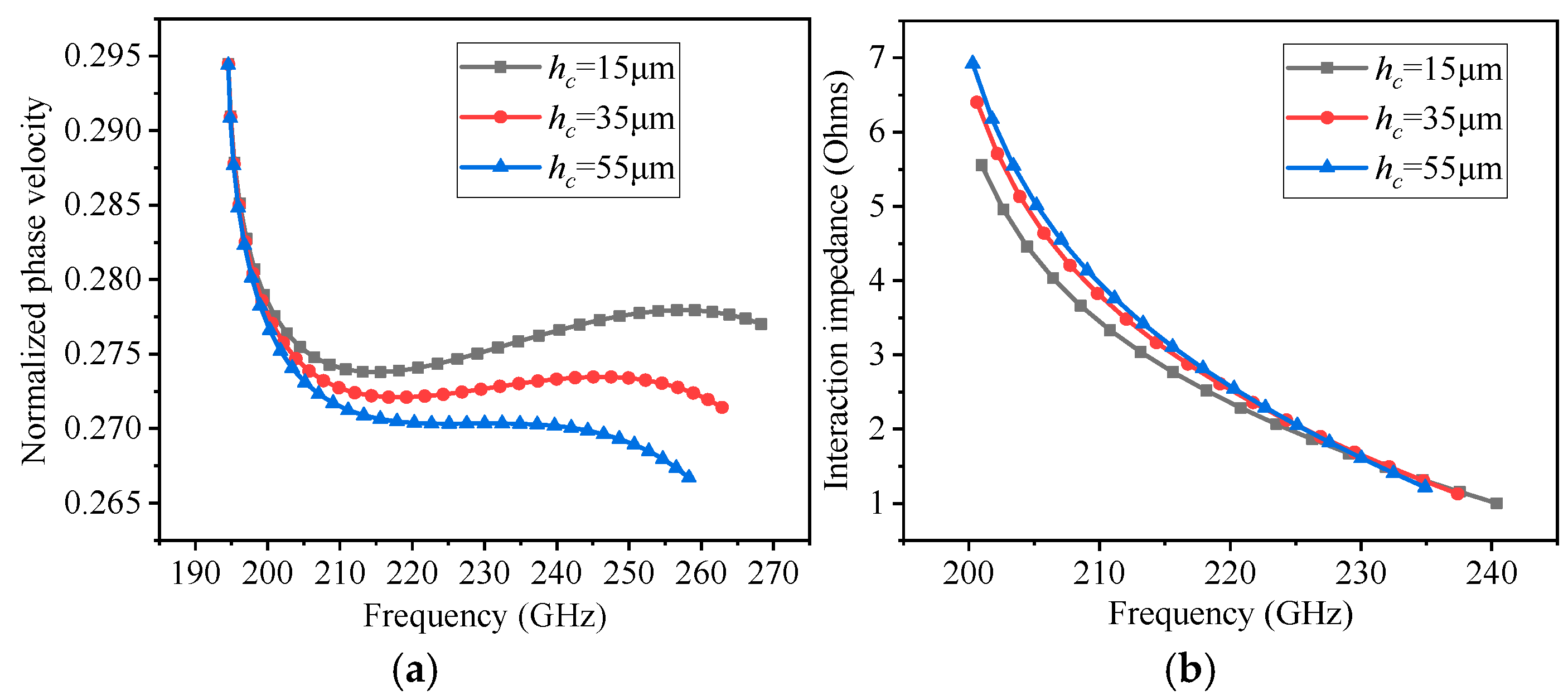
2.1. Geometry and Dispersion Characteristics of a Flat-Roofed SWG SWS

Depicted in Figure 1 are the perspective and side views of the flat-roofed SWG SWS model, where the waveguide’s width is denoted by a, and its height is represented by b. The oscillating amplitude is indicated by h, while p signifies the oscillating period. Additionally, the height of the sheet beam tunnel is marked as hb. Shown in Figure 1 is the evolution of the flat-roofed SWG SWS from the conventional SWG SWS, achieved through the compression of the waveguide height and the flattening of the sine-shaped metal gratings’ peaks. Illustrated in Figure 1b is hc, which denotes the height of the flattened section.
Utilized in the analysis of the flat-roofed SWG SWS’s slow-wave characteristics is the eigenmode solver, which employs master and slave boundaries. The flat-roofed SWG SWS has been designed in our analysis to ensure a wide synchronism region across the frequency range of 200–260 GHz. The electron beam is assumed to operate at a voltage of 20.8 kV, with the sheet beam tunnel height set to 140 μm. Therefore, the refined structural parameters are partly obtained as shown in Table 1, such as a, p, h, and hb.
The frequency-dependent dispersion characteristics and interaction impedances are simulated for various values of hc. From Figure 2a, it can be observed that as hc is increased from 15 μm to 55 μm, the cold bandwidth experiences a slight expansion, while the dispersion curve exhibits a more pronounced slope. As hc is varied from 15 μm to 55 μm, the interaction impedances initially rise and subsequently decline, as illustrated in Figure 2b. At hc = 35 μm, the interaction impedances reach their peak values within the frequency range of 200–260 GHz. Hence, a balance must be struck between the dispersion characteristics and interaction impedance in our design approach. To optimize the interaction impedance, the height hc is chosen as 35 μm, as specified in Table 1.

2.2. Transmission Characteristics of One-Stage Sheet Electron Beam Flat-Roofed SWG TWT

Transmission loss in SWS is a crucial factor for the performance of vacuum electron devices. Therefore, we conducted a thorough analysis of the transmission properties of the flat-roofed SWG. Specifically, we established a loss calculation model for the flat-roofed SWG slow-wave circuit within the CST Microwave Studio (MWS) environment. Figure 3 illustrates the transmission model of flat-roofed SWG, which consists of 55 periods in the main section and six periods in a gradually tapered section. In this figure, port 1 serves as the input port, while port 2 functions as the output port. Additionally, the impact of surface imperfections on metallic walls was also considered, as these imperfections can lead to increased losses and influence the overall transmission performance. Therefore, in order to more accurately simulate the waveguide transmission under actual conditions, the model’s material was configured as oxygen-free copper, exhibiting a conductivity of 3.0 × 10⁷ S/m [18].
Utilizing the simulation method, the S-parameter of the flat-roofed SWG slow-wave circuit can be determined across the operational frequency range spanning from 210 to 230 GHz. Upon examining Figure 4, it becomes evident that the transmission properties of the flat-roofed SWG rival those of the conventional SWG, demonstrating equally impressive performance characteristics. This comparison highlights that a flat-roofed SWG, like a conventional SWG, can achieve the efficient transmission of electromagnetic waves [19].
The results obtained through simulations using CST MWS indicate that the high-frequency system’s reflection coefficient remains below −25 dB (S11 < −25 dB), demonstrating excellent impedance matching and minimal signal reflection. Furthermore, the transmission loss is maintained at less than −1.1 dB (S21 > −1.1 dB) across a broad frequency range spanning from 200 GHz to 280 GHz. This performance level signifies that the system is capable of efficiently transmitting signals with minimal attenuation over this wide bandwidth, which is highly beneficial for applications requiring high-speed data transmission and low-loss signal processing.

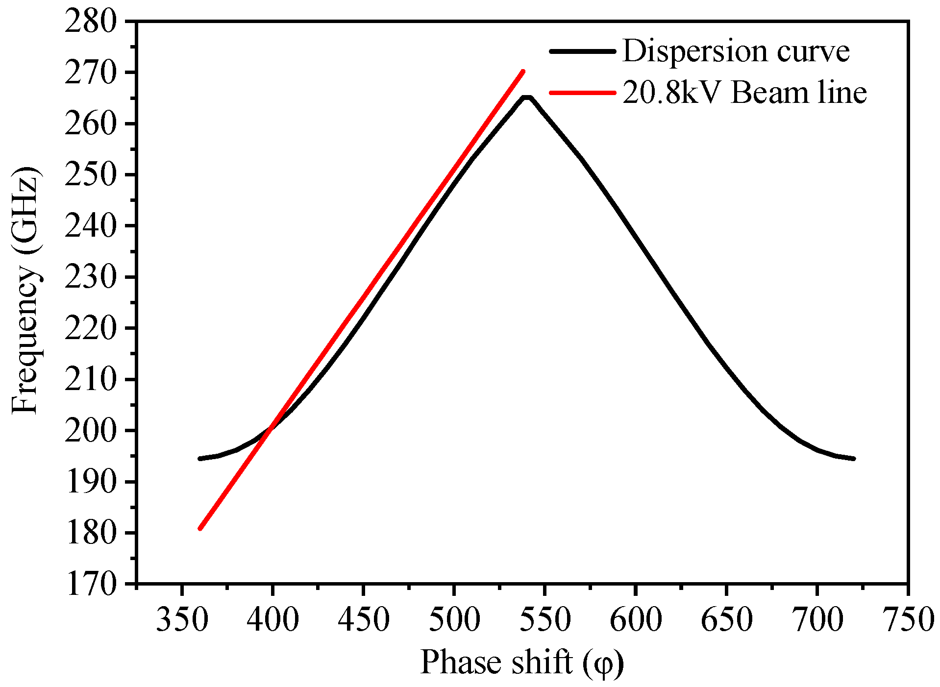
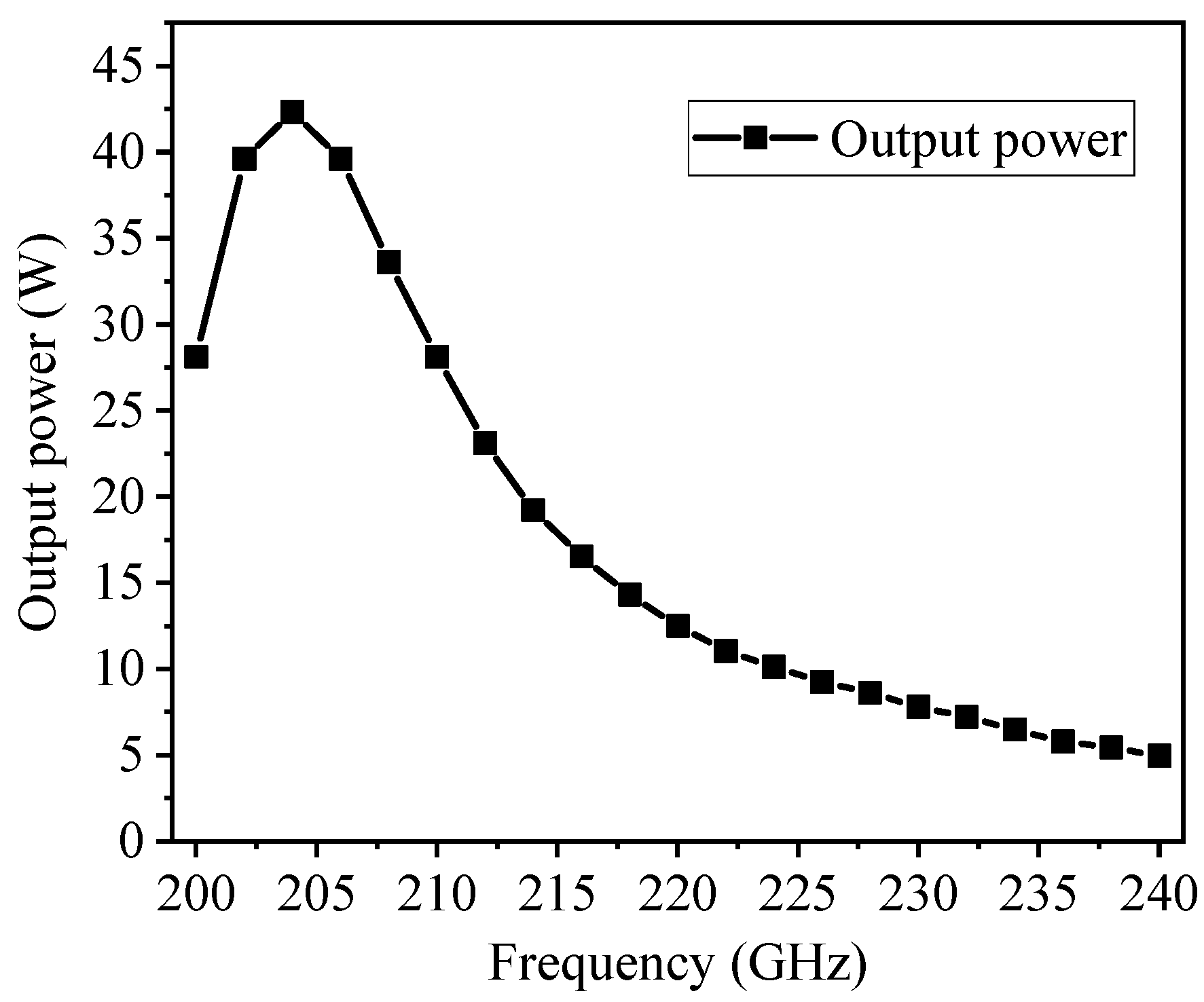
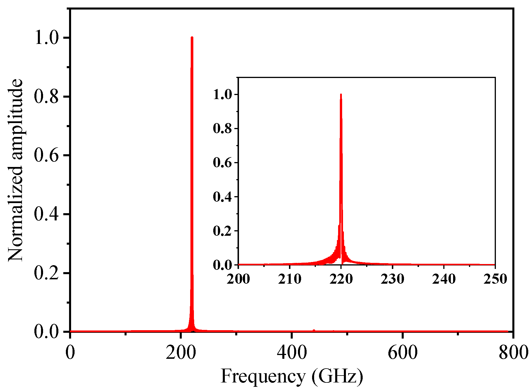
2.3. Beam–Wave Interaction of Flat-Roofed SWG TWT

After optimization, the final dispersion curve is presented in Figure 5. To ensure a broad synchronism region centered around 220 GHz, a beam voltage of 20.8 kV was selected. To further investigate the beam–wave interaction, an interaction simulation model was constructed within CST Particle Studio. Illustrated in Figure 6 are the input and output signal amplitudes, monitored at the corresponding ports of the Particle-In-Cell (PIC) simulation model. Upon observing the simulation results, it is evident that the output signal stabilizes after approximately 0.9 ns of the beam–wave interaction. Notably, the input signal, which is initially at 0.31622 V, undergoes amplification to reach 5.5 V, resulting in a gain of 24.8 dB. Additionally, the output power is measured to be approximately 15 W. These findings highlight the effectiveness of the optimized design in achieving significant signal amplification and power output within the desired frequency range, making it suitable for applications requiring high-power microwave generation and amplification.
To investigate the saturation output performance of the flat-roofed SWG TWT, simulations were conducted at 220 GHz by incrementally increasing the input power until the flat-roofed SWG TWT reached its saturation state. As illustrated in Figure 7, the flat-roofed SWG TWT demonstrated an output power of 13.7 W at an input power of 50 mW, and 89.7 W at an input power of 500 mW. Within the input power range of 50 mW to 500 mW, the output power exhibited a linear increase in response to the rising input power. Saturation was achieved at an input power of 2 W, where the maximum output power reached 128 W. Beyond this point, further increases in the input power drove the TWT into an over-saturation regime, resulting in a subsequent decline in the output power. These findings highlight the importance of optimizing the input signal power to ensure the TWT operates at its saturation performance.
As illustrated in Figure 8, the flat-roofed SWG TWT’s power output, within the frequency range of 200 GHz to 240 GHz, is depicted under constant input power conditions of 50 mW. Across the entire frequency spectrum, the maximum output power of 42 W is observed at 204 GHz. Notably, the output power remains above 5 W throughout the entire frequency band.

3. Design and Cold Test of Broad Bandwidth Coupling Structure

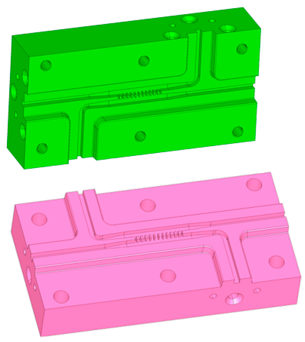
3.1. Analysis and Design of Broad Bandwidth Coupling Structure

Figure 9 depicts a representative model of a branch-guide broad bandwidth coupling structure, which comprises 12 branches, a primary waveguide, and a secondary waveguide. In this coupling structure, both the primary and secondary waveguides share dimensions of a × b. The spacing between the branches is denoted as p, whereas the branch widths, starting from the left and moving right, are specified as t1, t1 + dt,…, t1 + 4dt, t1 + 5dt, t1 + 4dt,…, t1 + dt, t1, respectively. The microwave signal is introduced into the system via port 1 in the primary waveguide and can be transferred to the secondary waveguide via port 2. The microwave signal is injected into the system through port 1 in the primary waveguide and can be transferred to the secondary waveguide via a sequence of carefully arranged branches. These branches serve as conduits, facilitating the transfer of the microwave signal from the primary waveguide to the secondary one, thus enabling efficient energy coupling between the two waveguides.
Among the various geometric parameters involved, p and t1 play pivotal roles in shaping the transmission characteristics of this coupling structure. Notably, the output waveguide of the first TWT, the input waveguide of the second TWT, and the waveguides comprising the coupling structure itself all share identical cross-sectional dimensions, measuring 0.885 mm by 0.7 mm (a × b). After meticulous optimization efforts, we arrived at the definitive dimensions for the remaining parameters. Specifically, the height h is set at 0.35 mm, the pitch p is 0.4 mm, the thickness t1 is determined to be 0.15 mm, and the displacement dt is 0.03 mm. The careful tuning of these dimensions ensures that the coupling structure operates efficiently and meets the desired coupling coefficient of 0 dB, thereby facilitating seamless signal transmission between the first TWT and the second TWT.
As illustrated in Figure 10, microwaves emitted from port 1 are efficiently and completely coupled to port 4 across a broad frequency range of 205 to 245 GHz. Considering the transmission loss (conductivity is set as 3 × 10⁷ S/m), it is noteworthy that within the frequency range of 210 GHz to 230 GHz, the transmission coefficient S41 consistently maintains an extremely high level, exceeding −0.2 dB. Meanwhile, the reflection coefficient S11, the directional coefficient S31, and the isolation coefficient S21 all exhibit values below −20 dB within the same frequency band. This indicates minimal reflection, minimal leakage to adjacent ports, and good isolation between the input port and the non-coupled output port. Furthermore, due to the significant attenuation of higher-order mode amplitudes, their impact is negligible, thereby ensuring a clean and efficient microwave transmission process.

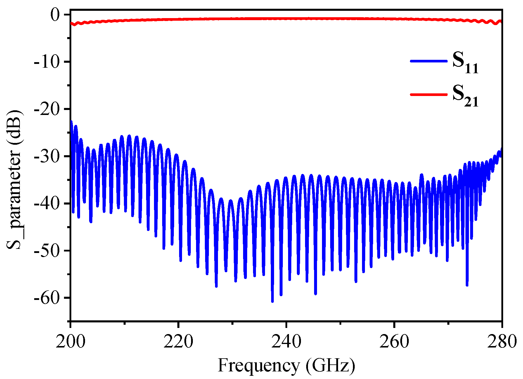
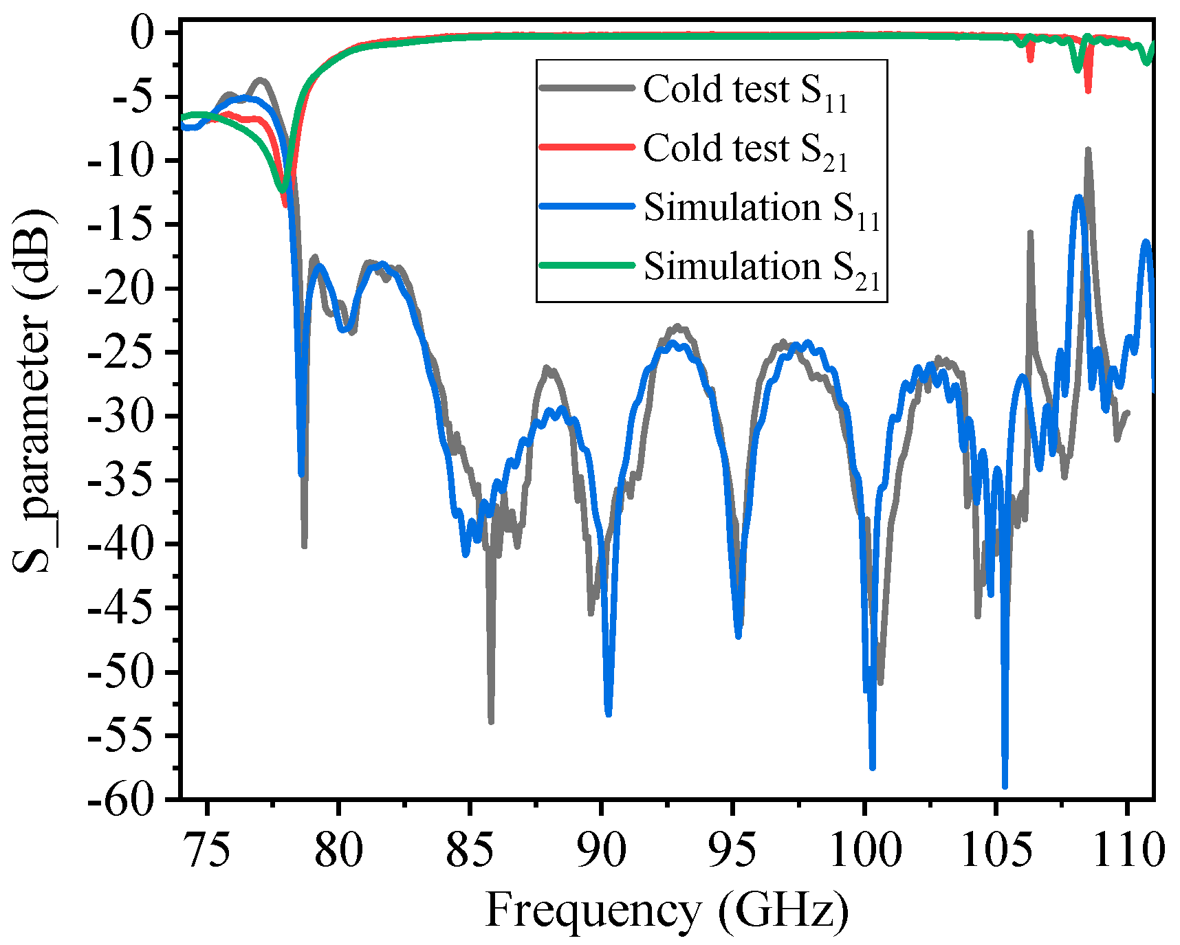
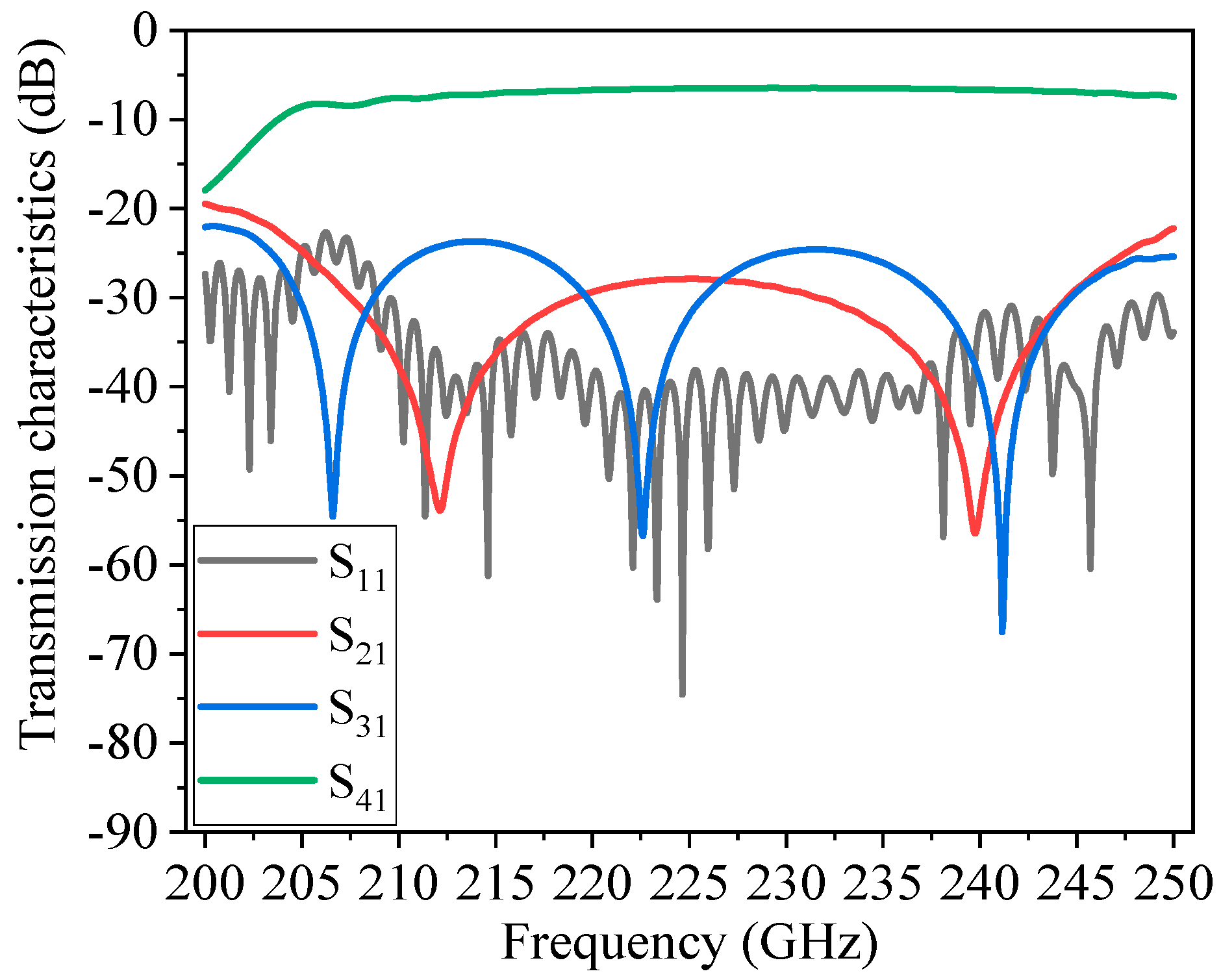
3.2. Cold Test of Broad Bandwidth Input/Output Coupling Structure

To validate the design and simulation results of the aforementioned coupling structure, a W-band coupling structure was designed, fabricated, and experimentally verified. For the convenience of testing, we designed a fabrication schematic as illustrated in Figure 11, which features port 2 and port 3 from Figure 9 being led out through bent waveguides and connected to matched loads during cold test. The coupling structure was processed using nano-CNC technology, with the splitting performed along the broad side of the waveguide to avoid severing the waveguide wall current, thereby ensuring the normal propagation and coupling of electromagnetic waves within the coupling structure. High-conductivity oxygen-free copper was employed to construct the two halves of the coupling structure. As shown in Figure 12a, the length of the coupling structure is 58.9 mm. The upper and lower parts of the structure are fixed by six pins. The internal image of the coupling structure is depicted in Figure 12b. On further enlargement, a clear view of the metal branch structure between the primary waveguide and the secondary waveguide can be observed, as illustrated in Figure 12c. Milling of the waveguide was performed using a 0.1 mm cutter head, with a spindle speed of approximately 42,000 revolutions per minute, achieving a machining accuracy of ±3 μm. As highlighted in Figure 12d, the cold test setup was assembled using a vector network analyzer (VNA) equipped with a W-band extended frequency module. Figure 13 shows the simulated and measured reflection parameters of the 94 GHz coupling structure for both the input and output ports. By comparison, the experimental and simulated reflection parameter results are basically consistent across the 85–105 GHz frequency range, less than −23 dB. This coupling structure has excellent transmission characteristics, with a transmission parameter S21 greater than −0.25 dB.

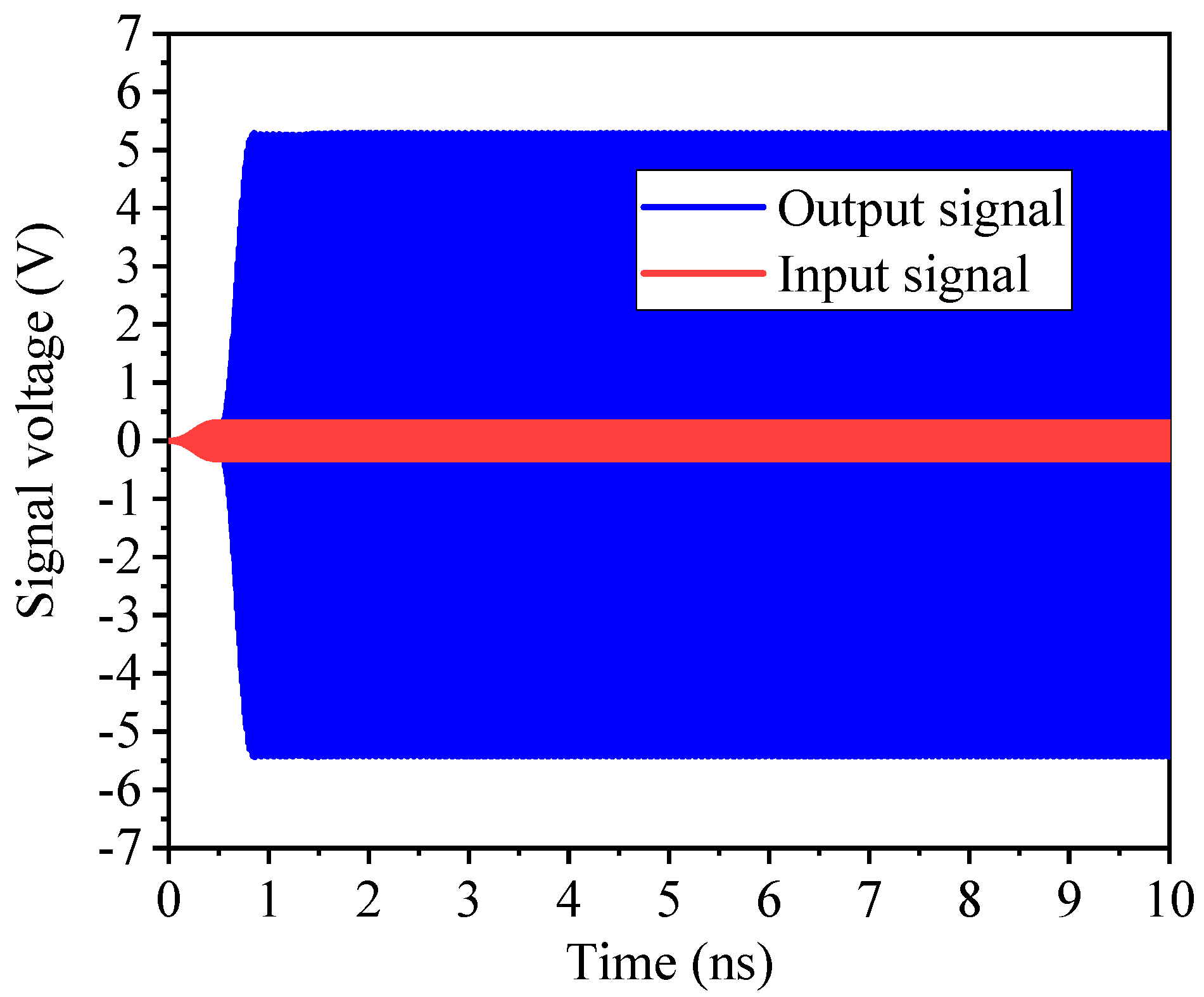
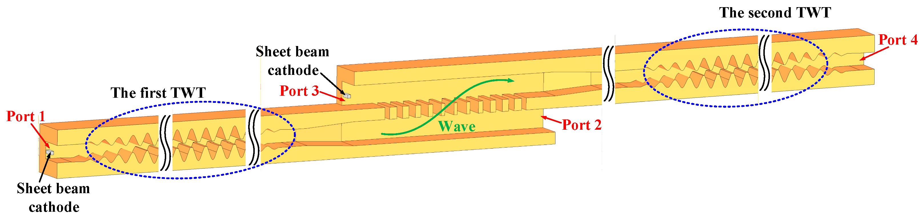
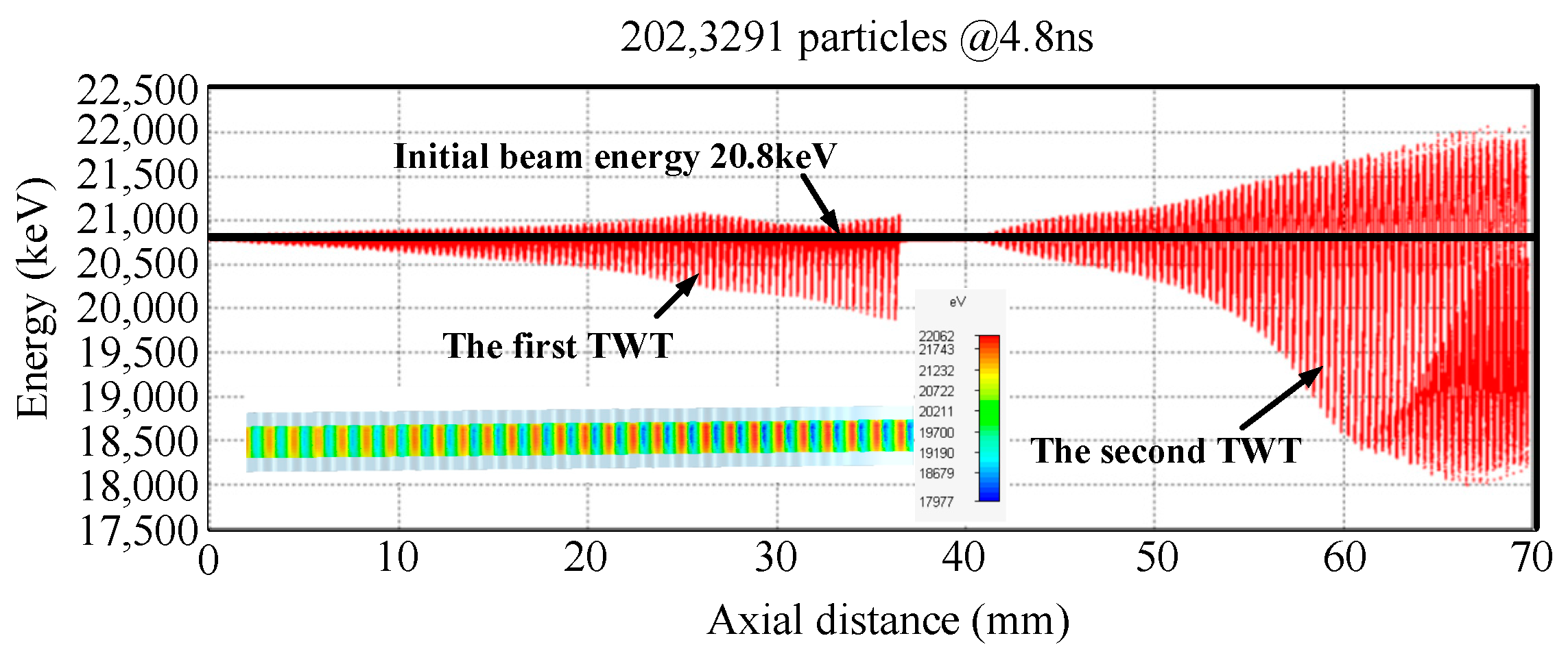
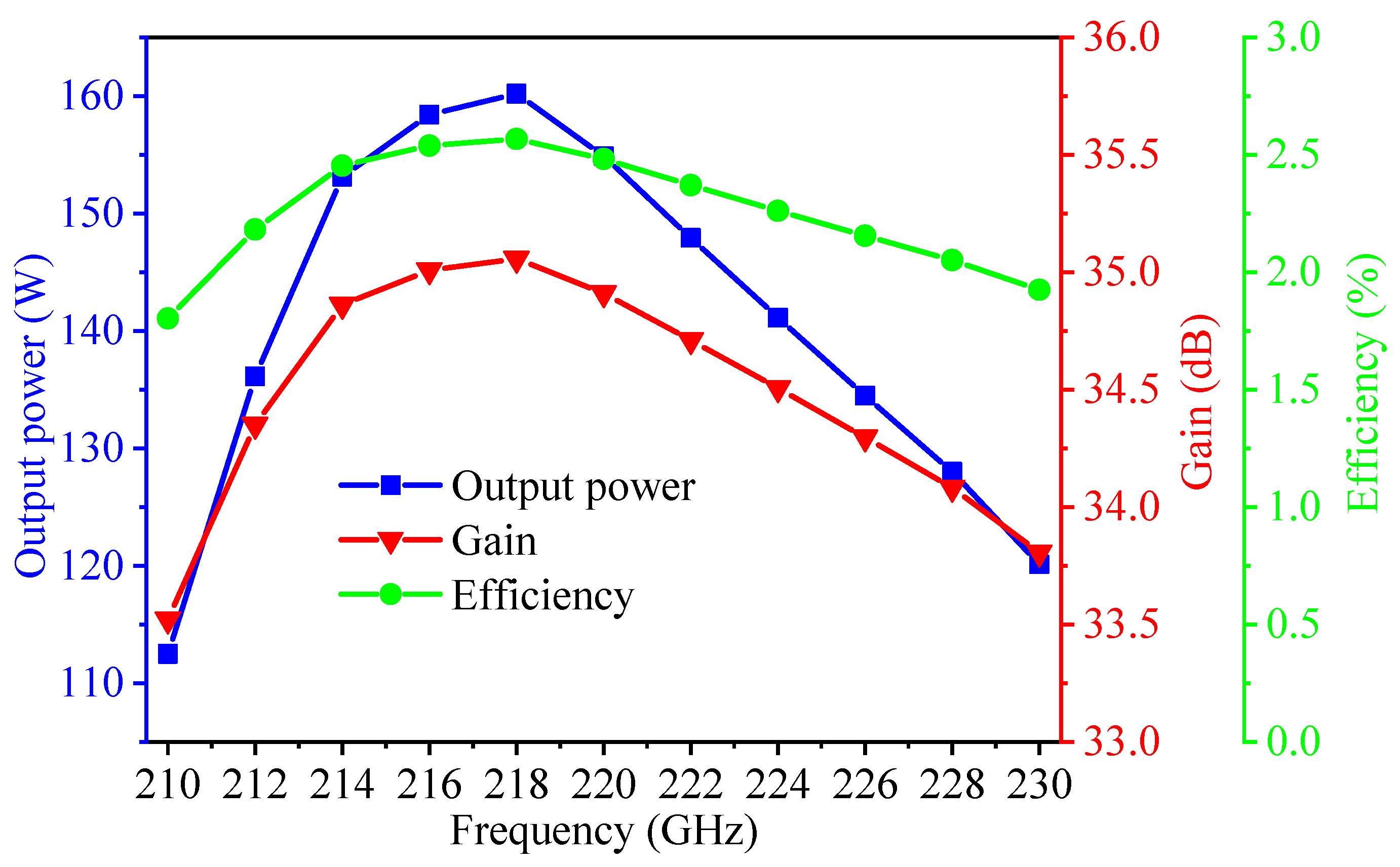
4. Simulation of the Beam–Wave Interaction of the Two-Stage Dual-Beam Flat-Roofed SWG TWT

Based on the previous research findings regarding the flat-roofed SWG and its coupling structure, this section further explores the design and performance of a two-stage cascaded flat-roofed SWG TWT. Figure 14 illustrates the three-dimensional schematic diagram of the device, whose core consists of two independent flat-roofed SWG TWT units. Each unit is equipped with a sheet beam cathode to facilitate efficient electron beam injection and energy exchange. The device features four waveguide ports, as shown in Figure 14, which are used for the signal input, output, and cascade coupling. Specifically, the output signal from the first-stage flat-roofed SWG TWT is directly fed into the input of the second-stage flat-roofed SWG TWT through an optimized coupling structure, thereby achieving the secondary amplification of the signal. To evaluate the transmission characteristics of this structure, detailed simulation calculations were conducted on the two-stage flat-roofed SWG slow-wave circuit, taking into account the actual material losses (with an effective conductivity of 3.0 × 10⁷ S/m) [18]. The simulation results are presented in Figure 15, which shows the transmission characteristics and loss profile of the signal within the two-stage structure. Within the 200 GHz to 250 GHz frequency range, the simulation results indicate that both S21 and S31 are below −20 dB, indicating minimal electromagnetic wave leakage from ports 2 and 3. Within the 210 GHz to 250 GHz frequency band, the reflection coefficient S11 is below −30 dB, demonstrating that the two-stage flat-roofed SWG with a coupling structure exhibits very low reflection. Furthermore, across the 210 GHz to 240 GHz frequency range, S21 is greater than −7.58 dB, with a unit loss of 1.73 dB/cm.
The PIC solver in CST PS is widely used to investigate the interaction dynamics in TWTs, providing a high-precision simulation tool for analyzing the energy exchange between the electron beam and the EM field. Based on the structural parameters determined from the electromagnetic simulations described earlier, this study preliminarily constructed a flat-roofed SWG TWT model suitable for the G-band, with its three-dimensional structure shown in Figure 14. In the simulation setup, employed in the simulation was a sheet electron beam featuring a cross-sectional area of 300 × 100 μm2, operating at a voltage of 20.8 kV and delivering a beam current of 150 mA. Simultaneously, applied at the input port was a high-frequency signal with a driving power of 50 mW. To ensure effective focusing and electron beam transmission, a uniform axial magnetic field of 1.0 Tesla was introduced.
To maximize the output power at the target frequency of 0.22 THz, systematic optimization was performed on the two-stage flat-roofed SWG TWT with a coupling structure. By incrementally increasing the number of periods in the slow-wave circuit, the optimal configuration was determined to be 55 periods for the first-stage TWT and 40 periods for the second-stage TWT. This optimized design not only maximizes the output power but also ensures efficient signal transmission and amplification across the two-stage structure. Figure 16, Figure 17, Figure 18 and Figure 19 present the typical PIC simulation results of the two-stage flat-roofed SWG TWT with a coupling structure at 0.22 THz. The simulation results demonstrate excellent beam–wave interaction characteristics at the target frequency, validating its high gain and stability in the terahertz frequency range.
Figure 16 illustrates the time-domain amplitude characteristics of the input and output signals observed at their respective ports. As observed in the figure, the output signal stabilizes after 1.3 ns, with the input signal amplitude amplified from 0.31622 V to 17.57 V, corresponding to a gain of 34.9 dB. This demonstrates the excellent signal amplification capability of the designed traveling-wave tube (TWT). To further analyze the spectral characteristics of the output signal, a Fourier transform was performed, and the outcomes illustrated in Figure 17. The spectral analysis indicates that the output signal exhibits high spectral purity at 220 GHz, confirming that the two-stage TWT does not generate harmonic signals during operation.
Figure 18 shows the distribution characteristics of electron energy along the axial distance when the electron dynamic system reaches a steady state at 4.8 ns. From the energy distribution curve, it can be seen that after the beam–wave interaction, most electrons lose part of their kinetic energy during the interaction process. This energy is efficiently imparted to the high-frequency EM field, thereby achieving radio frequency signal amplification. The inset vividly demonstrates the electron bunching effect at the conclusion of the beam–wave interaction circuit, which is a crucial physical phenomenon for efficient energy conversion in TWTs.
Figure 19 presents the output signal power and gain curve of the two-stage flat-roofed SWG TWT with a coupling structure. Through an optimized design, the two electron beams achieve sufficient energy exchange in the SWS, and the input signal exhibits excellent output characteristics within the operating frequency range after two-stage amplification. The simulation results indicate that within the frequency band range of 210–230 GHz, the two-stage flat-roofed SWG TWT with a coupling structure achieves an output power surpassing 112 W, with a maximum output power of 160 W achieved at 218 GHz. Additionally, the gain curve indicates that the TWT has a 3 dB bandwidth exceeding 20 GHz. The maximum beam–wave interaction efficiency of the two-stage TWT reaches 2.56%. When considering the efficiency of the collector, the overall efficiency of the two-stage TWT can be further enhanced. This outstanding broadband performance makes it highly valuable for applications in terahertz communication and imaging systems, providing important technical references for advancing next-generation terahertz vacuum electronic devices.
Compared to other SWG TWT designs, the two-stage TWT with the energy coupling structure proposed in this paper demonstrates significant advantages in several aspects. Firstly, the total length of this design is only 50 mm, significantly shorter than the 64 mm design in Ref. [20], which not only simplifies electron beam focusing, but also greatly enhances the practical manufacturability of the device, especially in the terahertz frequency band where miniaturization is critical. Secondly, this design eliminates the use of traditional attenuators, whereas Ref. [20] relies on attenuators to achieve stable operation, which is difficult to implement in small terahertz devices and increases manufacturing complexity and the risk of performance instability. The coupling structure in this paper can be fabricated integrally with the SWS of the TWT, offering a simpler and more reliable solution that effectively avoids the issues associated with attenuators. Thirdly, the coupling structure ensures output power stability by suppressing oscillations, while Ref. [21], due to the absence of attenuation or interruption measures, suffers from an unstable output power despite the excellent simulated performance (253 W output power, 37.04 dB gain). The two-stage TWT with the energy coupling structure achieves a better balance between performance, stability, and manufacturability, providing a more compact, stable, and practical design solution for the real-world application of terahertz TWTs.

5. Conclusions

This paper presents a comprehensive study on the development of a high-performance terahertz TWT based on flat-roofed SWG and coupling structure. Initially, the SWS of a 220 GHz flat-roofed SWG was optimized and analyzed, with particular emphasis on its transmission characteristics and the output performance of a single-stage flat-roofed SWG TWT. Subsequently, a novel waveguide-based coupling structure was proposed and thoroughly investigated through numerical simulations. The coupling structure was fabricated using nano-CNC technology, and the experimental measurements demonstrated an excellent agreement with the simulation results, confirming its superior transmission performance. Finally, a two-stage TWT incorporating the flat-roofed SWG and coupling structure was designed and simulated. The device exhibited a remarkable performance, achieving a maximum output power of 160 W within the frequency range of 210–230 GHz and a 3 dB bandwidth exceeding 20 GHz. This research on a two-stage TWT with an optimized coupling structure establishes a significant foundation for the development of terahertz TWTs with a higher power capacity and broader bandwidth, paving the way for advanced applications in terahertz communication and imaging systems.

Author Contributions

Investigation, Z.W.; Data curation, J.L. and T.W.; Writing—original draft, S.F.; Writing—review & editing, R.X.; Project administration, F.S. All authors have read and agreed to the published version of the manuscript.

Funding

This work was supported by the Key-Area Research and Development Program of Guangdong Province under Grant 2022B0701180002.

Data Availability Statement

The original contributions presented in this study are included in the article. Further inquiries can be directed to the corresponding author.

Conflicts of Interest

The authors declare no conflict of interest.

References

  1. Song, H.-J.; Lee, N. Terahertz Communications: Challenges in the Next Decade. IEEE Trans. Terahertz Sci. Technol. 2022, 12, 105–117. [Google Scholar]
  2. Siegel, P.H. Terahertz Technology in Biology and Medicine. IEEE Trans. Microw. Theory Tech. 2004, 52, 2438–2447. [Google Scholar]
  3. Guerboukha, H.; Nallappan, K.; Skorobogatiy, M. Toward Real-Time Terahertz Imaging. Adv. Opt. Photonics 2018, 10, 2018. [Google Scholar]
  4. Leitenstorfer, A.; Moskalenko, A.S.; Kampfrath, T.; Kono, J.; Castro-Camus, E.; Peng, K.; Qureshi, N.; Turchinovich, D.; Tanaka, K.; Markelz, A.G.; et al. The 2023 Terahertz Science and Technology Roadmap. J. Phys. D Appl. Phys. 2023, 56, 223001. [Google Scholar] [CrossRef]
  5. Jiang, Y.; Li, G.; Ge, H.; Wang, F.; Li, L.; Chen, X.; Lu, M.; Zhang, Y. Machine Learning and Application in Terahertz Technology: A Review on Achievements and Future Challenges. IEEE Access 2022, 10, 53761–53776. [Google Scholar] [CrossRef]
  6. Shu, G.; Pan, H.; Xie, X.; Ma, S.; Tang, J.; Liu, S.; Li, M.; Ruan, C.; He, W. Study of Magnetic Focusing Structures for 220 GHz Sheet Beam Traveling Wave Tubes. IEEE Trans. Terahertz Sci. Technol. 2025, 15, 120–127. [Google Scholar] [CrossRef]
  7. Duan, J.; Lu, Z.; Gao, P.; Wang, Z.; Guo, J.; Dong, Y.; Zheng, Y.; Wang, Z.; Wang, S.; Gong, H.; et al. Quadruple Folded Groove-Guide Slow Wave Structure with Power Synthesis Circuit for Terahertz TWT. IEEE Electron Device Lett. 2025, 46, 302–305. [Google Scholar]
  8. Lyu, Z.; Dong, J.; Jiang, S.; Jin, D.; Sun, S.; Tang, T.; Wang, Z.; Gong, H.; Gong, Y.; Zhang, C.; et al. Performing Intelligent Design of Broadband Pillbox Window for a Terahertz Traveling-Wave Tube by Using Physics-Informed Neural Network and Genetic Algorithm. IEEE Trans. Electron Devices 2024, 71, 4998–5004. [Google Scholar]
  9. Jiang, S.; Tang, X.; Huang, S.; Lyu, Z.; Wang, Z.; Tang, T.; Gong, H.; Gong, Y.; Duan, Z. Metamaterial-Inspired 0.22 THz Traveling-Wave Tubes with Double Sheet Beams. IEEE Trans. Electron Devices 2023, 70, 1306–1311. [Google Scholar]
  10. Zhang, X.; Cai, J.; Zhang, X.; Du, Y.; Gao, C.; Mu, H.; Feng, J. Four-Port Folded Waveguide Slow Wave Structure for W-Band 1-kW Pulsed Traveling Wave Tube. IEEE Electron Device Lett. 2025, 46, 100–102. [Google Scholar]
  11. Jiang, S.; Yang, G.; Wang, Z.; Wang, X.; Zhang, X.; Lyu, Z.; Tang, T.; Gong, H.; Gong, Y.; Duan, Z. Experimental Investigation of a Shape-Optimized Staggered Double-Vane Slow-Wave Structure for Terahertz Traveling-Wave Tubes. IEEE Trans. Electron Devices 2022, 69, 4632–4637. [Google Scholar]
  12. Lee, J.; Choi, H.E.; Choi, W.; Choi, E. Advanced Bragg Resonator Integration for Enhanced Bandwidth and Stability in G-Band TWT with Staggered Double Vane Structure. IEEE Trans. Electron Devices 2025, 72, 459–466. [Google Scholar] [CrossRef]
  13. Fang, S.; Xu, J.; Yin, H.; Lei, X.; Jiang, X.; Yin, P.; Wu, G.; Yang, R.; Li, Q.; Guo, G.; et al. Experimental Verification of the Low Transmission Loss of a Flat-Roofed Sine Waveguide Slow-Wave Structure. IEEE Electron Device Lett. 2019, 40, 808–811. [Google Scholar] [CrossRef]
  14. Yan, S.; Su, W.; Wang, Y.; Xu, A. Design and Theoretical Analysis of Multibeam Folded Waveguide Traveling-Wave Tube for Subterahertz Radiation. IEEE Trans. Plasma Sci. 2015, 43, 414–421. [Google Scholar] [CrossRef]
  15. Zhang, X.; Feng, J.; Cai, J.; Du, Y.; Dong, R.; Wu, X. Power Enhancement in W-Band Pulsed Folded Waveguide TWT. IEEE Trans. Electron Devices 2021, 68, 2504–2508. [Google Scholar]
  16. Gong, Y.; Yin, H.; Yue, L.; Lu, Z.; Wei, Y.; Feng, J.; Duan, Z.; Xu, X. A 140-GHz Two-Beam Overmoded Folded-Waveguide Traveling-Wave Tube. IEEE Trans. Plasma Sci. 2011, 39, 847–851. [Google Scholar]
  17. Zhou, K.; Feng, J. Cold Characteristics of Overmoded Ridge- and Groove-Loaded Folded Waveguides for High-Power Traveling Wave Tubes. IEEE Trans. Plasma Sci. 2021, 49, 4009–4016. [Google Scholar]
  18. Zhang, J.; Xu, J.; Cai, J.; Yue, L.; Yin, H.; Xu, Y.; Yin, P.; Luo, J.; Zhao, G.; Wang, W.; et al. A Novel Non-Quasi-2D Slow-Wave Structure for THz Sheet Beam TWTs. IEEE Electron Device Lett. 2024, 45, 700–703. [Google Scholar] [CrossRef]
  19. Xu, X.; Wei, Y.; Shen, F.; Duan, Z.; Gong, Y.; Yin, H.; Wang, W. Sine Waveguide for 0.22-THz Traveling-Wave Tube. IEEE Electron Device Lett. 2011, 32, 1152–1154. [Google Scholar] [CrossRef]
  20. Zhang, L.; Ma, G.; Jiang, Y.; Lei, W.; Hu, P.; Tang, X.; Chen, H.; Wei, Y. Demonstration of a Double Flat-Roofed Sine Waveguide Slow Wave Structure with Low Loss for 220-GHz Traveling-Wave Tube. IEEE Micro. Wireless Technol. Lett. 2023, 33, 291–294. [Google Scholar] [CrossRef]
  21. Zhang, L.; Jiang, Y.; Lei, W.; Hu, P.; Guo, J.; Song, R.; Tang, X.; Ma, G.; Chen, H.; Wei, Y. A Piecewise Sine Waveguide for Terahertz Traveling Wave Tube. Sci. Rep. 2022, 12, 10449. [Google Scholar] [CrossRef] [PubMed]
Figure 1. Three-dimensional representation and geometric specifications of the flat-roofed SWG SWS: (a) perspective view and (b) single flat-roofed SWG SWS.
Electronics 14 01756 g001
Figure 2. Graphs depicting (a) normalized phase velocities and (b) interaction impedances for varying values of hc.
Electronics 14 01756 g002
Figure 3. Model used for computing the transmission characteristics of the flat-roofed SWG.
Electronics 14 01756 g003
Figure 4. Reflection and transmission properties of the flat-roofed SWG.
Electronics 14 01756 g004
Figure 5. Dispersion curve characteristics and beam line of the flat-roofed SWG SWS.
Electronics 14 01756 g005
Figure 6. Output signal and input signal of one-stage flat-roofed SWG TWT at 220 GHz.
Electronics 14 01756 g006
Figure 7. Output power of a single-stage flat-roofed SWG TWT at different input powers.
Electronics 14 01756 g007
Figure 8. Power output from a single-stage flat-roofed SWG TWT.
Electronics 14 01756 g008
Figure 9. Three-dimensional model of the coupling structure.
Electronics 14 01756 g009
Figure 10. Transmission and reflection characteristics of coupling structure.
Electronics 14 01756 g010
Figure 11. Schematic diagram of coupling structure.
Electronics 14 01756 g011
Figure 12. (a) Fabricated coupling structure. (b) Internal structure of coupling structure. (c) Branches of coupling structure. (d) Cold test setup for coupling structure.
Electronics 14 01756 g012
Figure 13. Comparison of S-parameter measurements from experiments and simulations.
Electronics 14 01756 g013
Figure 14. Three-dimensional simulation model of the two-stage flat-roofed SWG TWT with a coupling structure.
Electronics 14 01756 g014
Figure 15. Transmission properties of the two-stage flat-roofed SWG TWT with a coupling structure.
Electronics 14 01756 g015
Figure 16. Input and output signals of the two-stage flat-roofed SWG TWT with a structure at 220 GHz.
Electronics 14 01756 g016
Figure 17. Spectrum of the output signal of two-stage flat-roofed SWG TWT with a coupling structure.
Electronics 14 01756 g017
Figure 18. Electron energy versus axial distance at 4.8 ns, with the inset showing electron bunching at the beam–wave interaction circuit’s end.
Electronics 14 01756 g018
Figure 19. Power output and gain characteristics of the two-stage flat-roofed SWG TWT with a coupling structure.
Electronics 14 01756 g019
Table 1. Optimized structure parameters of the flat-roofed SWG SWS for a 220 GHz TWT.
ParameterValue (μm)
a770
b500
p460
h215
hb140
hc35
Disclaimer/Publisher’s Note: The statements, opinions and data contained in all publications are solely those of the individual author(s) and contributor(s) and not of MDPI and/or the editor(s). MDPI and/or the editor(s) disclaim responsibility for any injury to people or property resulting from any ideas, methods, instructions or products referred to in the content.

