Communication

Sub-6 GHz GaAs SPDT Switch Co-Designed with Shunt Inductor for ESD Protection

1
Department of Intelligent Semiconductors, Soongsil University, Seoul 06978, Republic of Korea
2
Department of Electric Engineering, Soongsil University, Seoul 06978, Republic of Korea
*
Author to whom correspondence should be addressed.
Electronics 2025, 14(9), 1707; https://doi.org/10.3390/electronics14091707
Submission received: 23 March 2025 / Revised: 15 April 2025 / Accepted: 21 April 2025 / Published: 23 April 2025

Abstract

:
In this study, a single-pole double-throw (SPDT) switch for Sub-6 GHz application is designed. In particular, a shunt inductor is connected to the antenna port of the switch for ESD (electrostatic discharge) protection in RF (radio frequency) front end module. The shunt inductor not only serves as an ESD protection device, but also serves as a component of a parallel resonance circuit to suppress insertion loss of the switch. In addition, in order to secure the power handling capability, transistors turned off in the transmit (Tx) mode are implemented as quadruple-gate transistors. An SPDT switch is fabricated using GaAs pHEMT provided in the 500 nm GaAs BiFET process to verify the feasibility of the proposed switch structure. The operating frequency is set from 3 GHz to 5 GHz. The insertion loss and isolation measured in the Tx mode are lower than 0.35 dB and higher than 31.6 dB, respectively. The insertion loss and isolation measured in the Rx mode are lower than 0.32 dB and higher than 33.9 dB, respectively. The chip size including test pads is 0.890 × 0.875 mm2.

1. Introduction

Recently, with the commercialization of 5G mobile communication, the development of RF integrated circuits (ICs) in n77 and n79 bands is also actively progressing [1,2,3,4]. In particular, switches, power amplifiers (PAs), and low-noise amplifiers (LNAs) are key circuits constituting RF front-end module (FEM) [5,6,7]. Among them, a switch is a circuit that is directly connected to an antenna, and insertion loss, isolation, and power handling capabilities are the main performance indicators [8,9,10,11,12]. If the insertion loss of the switch deteriorates, the output power of the transmitted signal decreases and the noise figure of the received signal increases. Also, if the power handling capability of the switch is low, the output power of the PAs is not fully transmitted to the antenna. Therefore, research to achieve the performance of such a switch is constantly being conducted.
In addition, as shown in Figure 1, the switch is directly connected to the antenna in the FEM. Therefore, the possibility of electrostatic discharge (ESD) through the antenna port of the switch should be considered when manufacturing the communication system using a FEM or operating the system. Therefore, it is necessary to obtain the reliability of the FEM by applying an ESD protection solution to the antenna port of the switch [13]. As shown in Figure 1, when an ESD protection solution is applied to the antenna port of the switch, the output of the PA and the input of the LNA are free from an additional ESD protection. For ESD protection in the switch, design techniques using diodes have been introduced [14]. However, when using a diode as an ESD protection device, an additional design technique is required to remove the parasitic capacitance of the diode. As an example, in order to suppress the influence of the parasitic capacitance of the diode, a method of utilizing an additional LC tank has been proposed [15,16]. Shunt inductors can also be used as another ESD protection device in switches [13]. However, there is a problem that the use of shunt inductors for ESD protection deteriorates the performance of the switch. As such, the application of ESD protection techniques to RFICs is generally accompanied by deterioration in the performance of RFICs. As a result, there are often instances of the absence of ESD protection devices and circuits in the RFIC. Furthermore, even if the ESD protection technique is applied to the RFIC, it is common to apply the ESD protection technique after the design of the core circuit of the RFIC is completed. In other words, ESD protection techniques are generally designed somewhat independently of core circuits, and as a result, ESD protection devices and circuits are a major cause of deterioration of the performance of the RFIC.
In this study, we propose a co-design technique for switches and shunt inductors. Through the proposed co-design technique, shunt inductors are utilized for resonance in transmit (Tx) and receive (Rx) modes to suppress insertion loss as well as ESD protection. Because the shunt inductor of this study is co-designed with the matching network of the switch, performance degradation due to the shunt inductor can be successfully suppressed. In addition, in this study, unlike the typical LC tank technique, the capacitor for the LC tank is designed with parasitic capacitance generated by the switch itself, not an additional capacitor. Additionally, quadruple-gate transistors are asymmetrically used to secure power handling capabilities in the Tx mode.
In Section 2, the operation of the proposed single-pole double-throw (SPDT) switch using a shunt inductor for ESD protection is explained. In Section 3, simulation and measurement results are provided.

2. Proposed SPDT Switch with ESD Protection

First, a proposed ESD protection technique using a shunt inductor will be described. Then, the operation and design of the proposed switch with the shunt inductor will be provided.

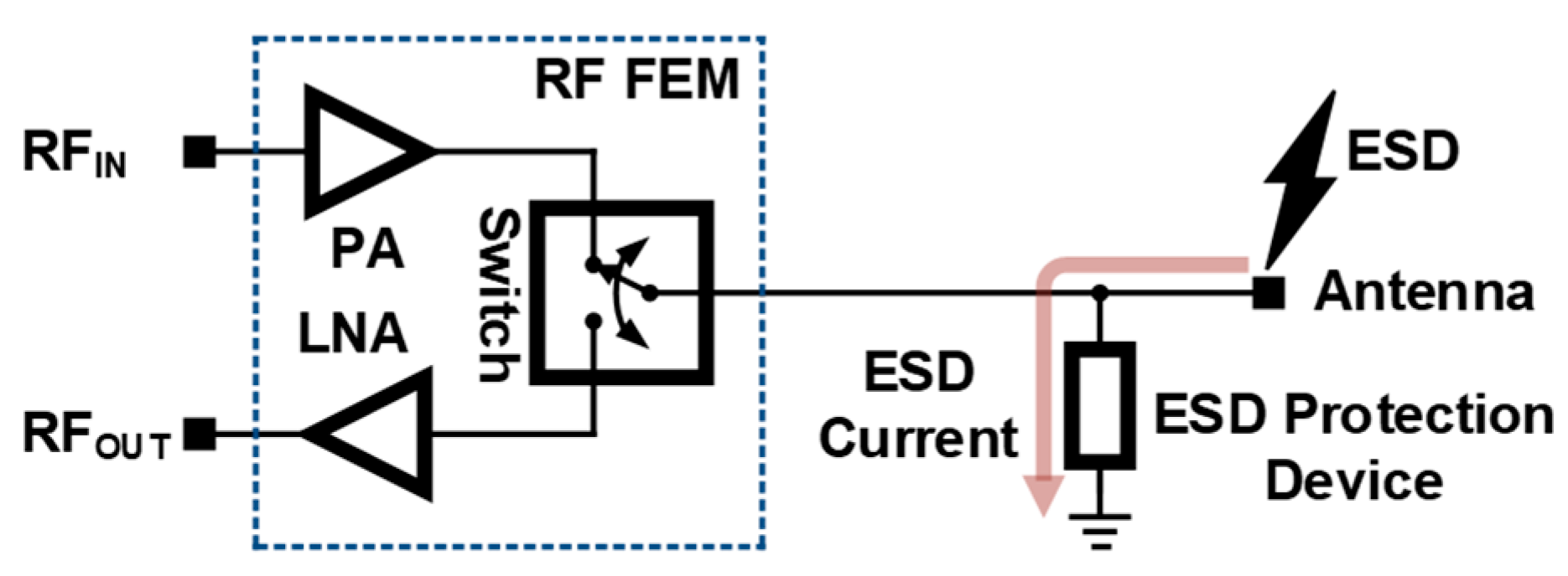
2.1. ESD Protection Technique Using Shunt Inductor

In the proposed switch, a shunt inductor is connected to the antenna port. The shunt inductor serves as an ESD protection device. In general, considering the frequency components of the human-body-model (HBM) and the machine-model (MM) of ESD, the impedance of the RF inductor from the perspective of ESD is negligible. In order to conceptually examine the effectiveness of the proposed ESD protection technique through ESD model, the internationally standardized HBM of Figure 2 is considered.
The HBM in Figure 2a consists of a charging resistor RC, a 100 pF capacitor, and a 1.5 kΩ resistor. When the switch in Figure 2a is connected to RC, the 100 pF capacitor is charged with a charge equivalent to VHBM. Then, if the switch is connected to the 1.5 kΩ resistor, the charge charged in the 100 pF capacitor is discharged through 1.5 kΩ resistor. Figure 2b shows the frequency response of the HBM ESD. The 6 dB bandwidth of the HBM ESD is from dc to 2.1 MHz, and 2.1 MHz is negligibly low compared to the operating frequency of a general RFIC.
In order to conceptually confirm the effectiveness of the proposed switch structure applying the ESD protection by connecting a shunt inductor between the antenna port and the ground, the shunt inductor, LESD, is connected to the output node of the ESD HMB as shown in Figure 2a. LESD operates as an inductive impedance for RF signals, but has a negligible impedance for an HBM ESD of 2.1 MHz, allowing ESD current to be easily shunted to the ground. For example, as shown in Figure 2, when IHBM, the HBM ESD current, flows through the LESD, the shunt inductor, the voltage drop at the LESD, VSL, is examined. Here, the frequency of the HBM ESD is set to 2.1 MHz and the LESD is set to 5 nH. Under such conditions, VSLpeak, which is the peak VSL, could be calculated as follows.
V S L , p e a k = ω L E S D 1.5 k + ω L E S D V H B M = 4.4 × 10 5 V H B M
From the results, the VSL,peak reaches only 4.4 V when the VHBM is 100 kV. Considering that a typical IC has a HBM ESD protection level of 2 kV or 8 kV, it has a sufficiently high ESD protection level when using a shunt inductor as an ESD protection device. This conclusion was successfully verified from previous studies through the measurement results of LNAs and PAs using shunt inductors or transformers as ESD protection devices [17,18]. In this study, the effectiveness of the proposed ESD protection technique is explained using HBM ESD, but previous studies have proven that shunt inductors have an ESD protection effect against MM ESD and as well as HBM ESD [17,18]. In this study, the width of the metal line constituting the LESD is 6 μm.
In summary, typical shunt inductor used in RFICs have negligible impedance in the frequency region of ESD HBM, which act as effective ESD protection devices. On the other hand, the shunt inductor in the general operation aspect of the RFIC provides useful impedance and could be used as a matching component for improving the performance of the RFIC. Therefore, in the proposed switch structure with ESD protection technique using LESD, the freedom to select LESD optimized for switch performance is easily secured even considering ESD survival level of the switch.

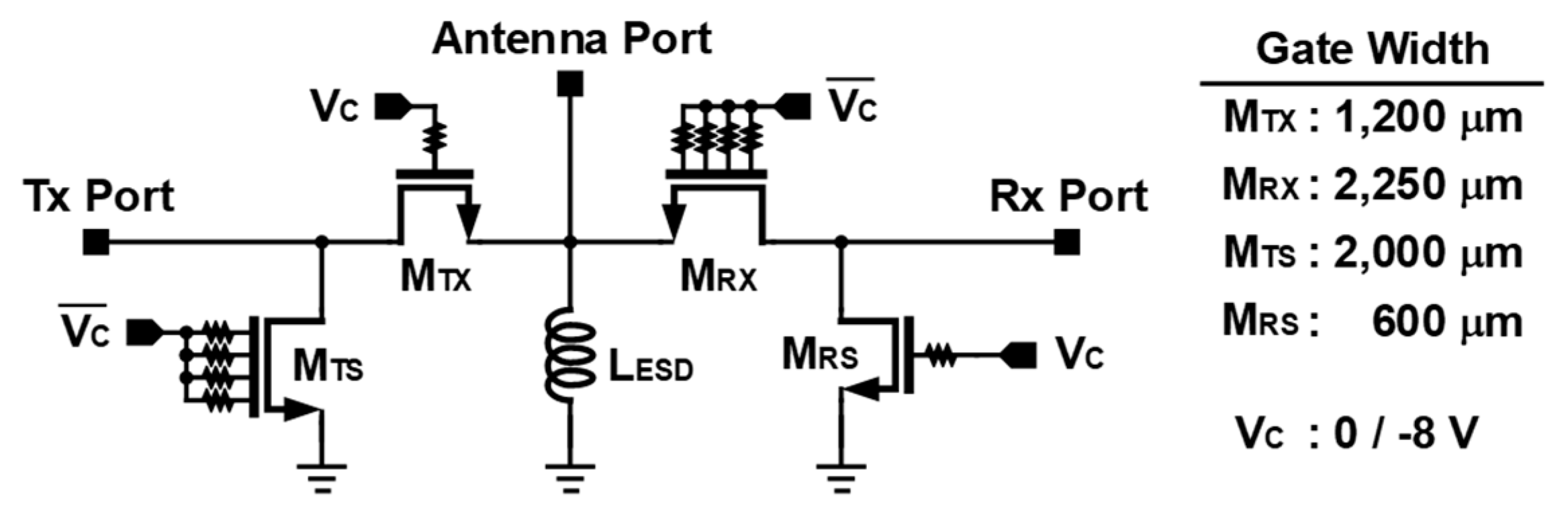
2.2. Operation of the Proposed SPDT Switch

Figure 3 shows the schematic of the proposed switch with ESD protection using LESD. For the Tx mode, VC, which is a control voltage, is low, MTS and MRX are turned off, and MTX and MRS are turned on. Because MTX serves to deliver Tx signals to the antenna port, MTX is designed as a single-gate transistor to minimize power loss. In addition, MRS is designed as a single-gate transistor to remove the leakage current flowing into the Rx port in the Tx mode. MTS and MRX, which are transistors turned off in the Tx mode, are designed as quadruple-gate transistors in order to secure power handling capabilities in the Tx mode. In the Rx mode, MRX and MTS are turned on as opposed to the Tx mode. However, because MRX and MTS are designed as quadruple-gate transistors, the gate width is sufficiently secured to suppress power loss and improve isolation by reducing on-resistance. Here, because the quadruple-gate transistor has the effect of stacking four transistors, the ability to withstand power is improved, thereby improving the power handling capability of the switch. However, the structure in which four transistors are stacked could deteriorate the performance of the switch due to parasitic components caused by metal lines used to connect each transistor. On the other hand, quadruple-gate transistors have the almost same effect as the structure in which four transistors are stacked in terms of power handling capability. However, quadruple-gate transistors have the advantage of reducing parasitic components caused by metal lines compared to the structure in which four transistors are stacked.
Figure 4 shows equivalent circuits in Tx and Rx modes. When each transistor is turned on and off, the transistors can be equivalent to on-resistances and off-capacitances, respectively.
In the Tx mode, assuming that the on-resistance RTX and RRS are small enough, LESD and CTS + CRX become a parallel resonance circuit. If the resonance frequency of the resonance circuit matches the frequency of the Tx signal, the Tx signal is successfully transmitted to the antenna port. In addition to the resonance of LESD and CTS + CRX, if the RTX is sufficiently small, insertion loss in the Tx mode could be suppressed. The RRS serves to shunt the Tx signal flowing to the Rx port to the ground; therefore, if the RRS is sufficiently small, isolation in the Tx mode could be secured.
Similarly to the Tx mode, in the Rx mode as well, the parallel resonance circuit forms a high impedance in the Rx signal frequency so that the Rx signal is successfully received at the Rx port. In addition to the resonance of LESD and CRS + CTX, if the RRX is sufficiently small, insertion loss in the Rx mode could be suppressed. The RTS serves to shunt the Rx signal flowing to the Tx port to the ground; therefore, if the RTS is sufficiently small, isolation in the Rx mode could be secured.
Therefore, sufficiently lowering the on-resistance of the transistor and resonance play an important role in improving the performance of the switch. ZTX,EQ and ZRX,EQ in Figure 4 for considering the resonance characteristics can be expressed as follows.
Z T X , E Q = j ω L E S D 1 ω 2 L E S D C E Q , T X , Z R X , E Q = j ω L E S D 1 ω 2 L E S D C E Q , R X
Here, CEQ,TX and CEQ,RX are CTS + CRX and CRS + CTX, respectively. In addition, in summary, it is ideal to match the resonant frequencies of each ZTX,EQ and ZRX,EQ, fTX and fRX, with the operating frequencies of the signal.
f T X = 1 2 π L E S D C E Q , T X , f R X = 1 2 π L E S D C E Q , R X
As a result, the LESD for ESD protection determines the operating frequency in each mode by resonance with CEQ,TX and CEQ,RX according to Tx and Rx modes, respectively. Considering the ideal operation of the SPDT switch, CEQ,TX and CEQ,RX should be the same in order for fTX and fRX to be the same. Therefore, CEQ,TX and CEQ,RX should be considered in determining the size of transistors.
In addition, when determining the size of the transistor, the on-resistance of the transistor should also be considered. In particular, RTX and RRX in Figure 4 directly affect insertion losses in Tx and Rx modes, respectively. In order to suppress insertion loss, the gate widths of MTX and MRX should be increased, but the increased gate width of the transistor increases CTX and CRX. The increased CTX and CRX increase CEQ,RX and CEQ,TX, respectively, causing the switch to shift the operating frequency. The shift in the operating frequency could be corrected by reducing the inductance of the LESD. However, a decrease in LESD could cause a decrease in the frequency bandwidth of the switch. In conclusion, the size of the transistor should be carefully set by comprehensively considering operating frequency, bandwidth, insertion loss and isolation.

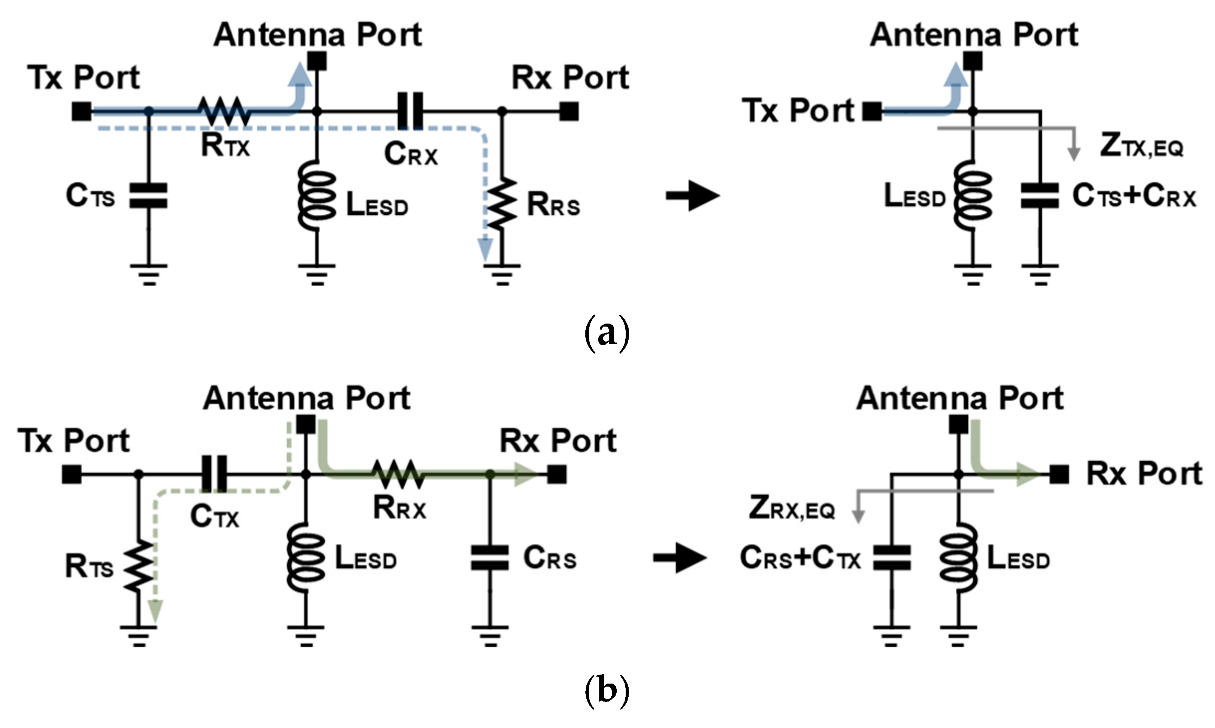
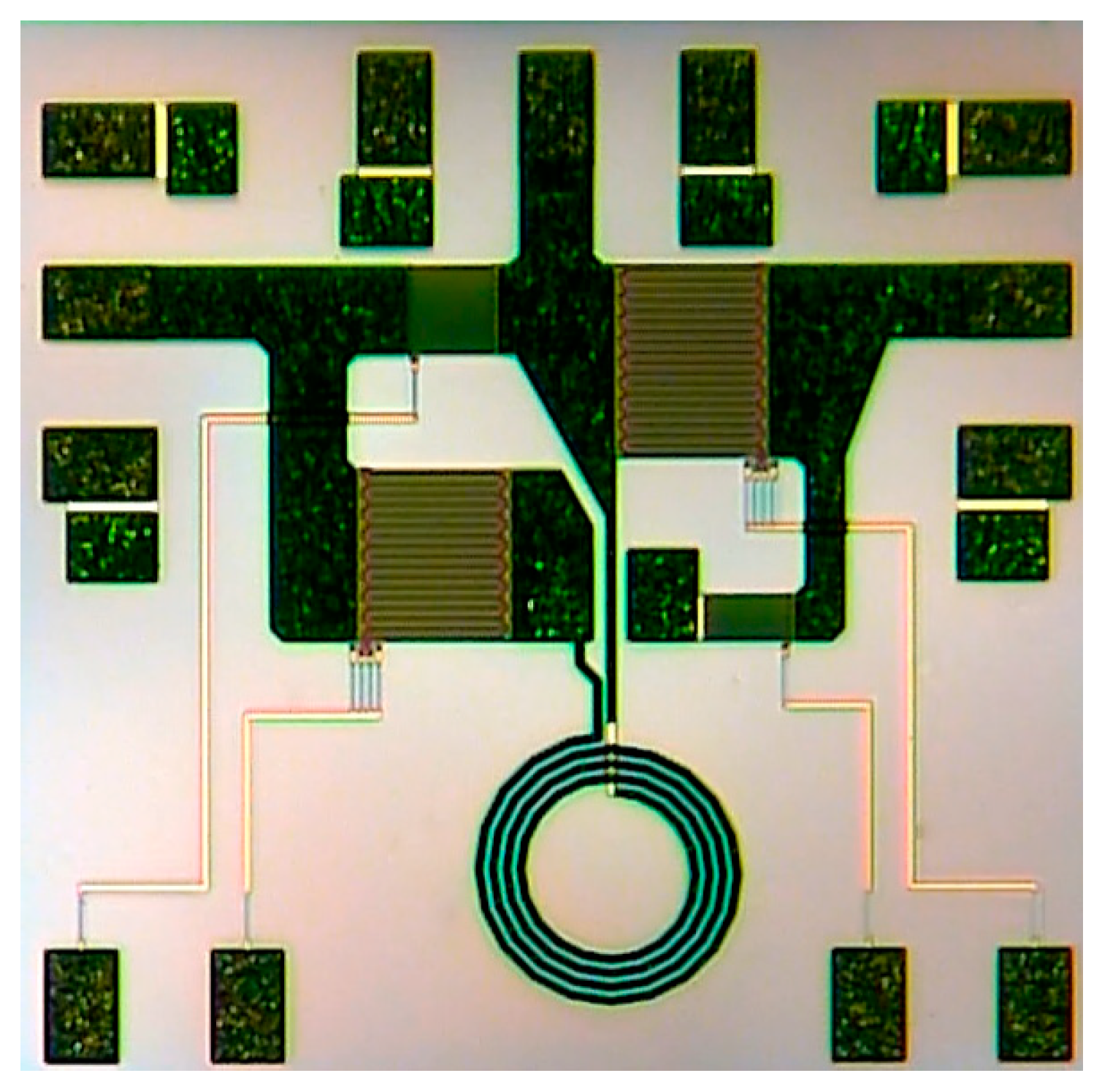
2.3. Design of the Proposed SPDT Switch
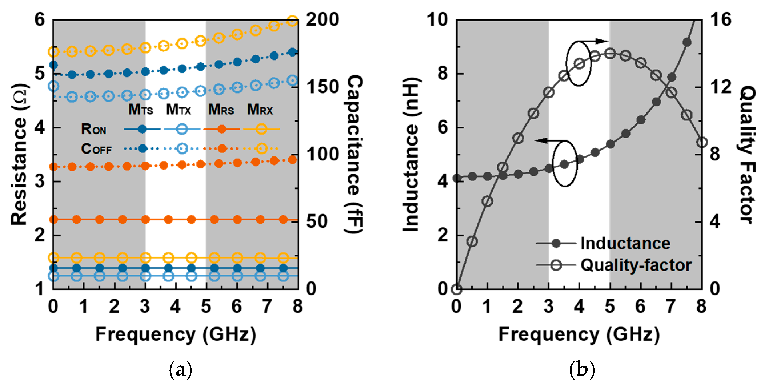
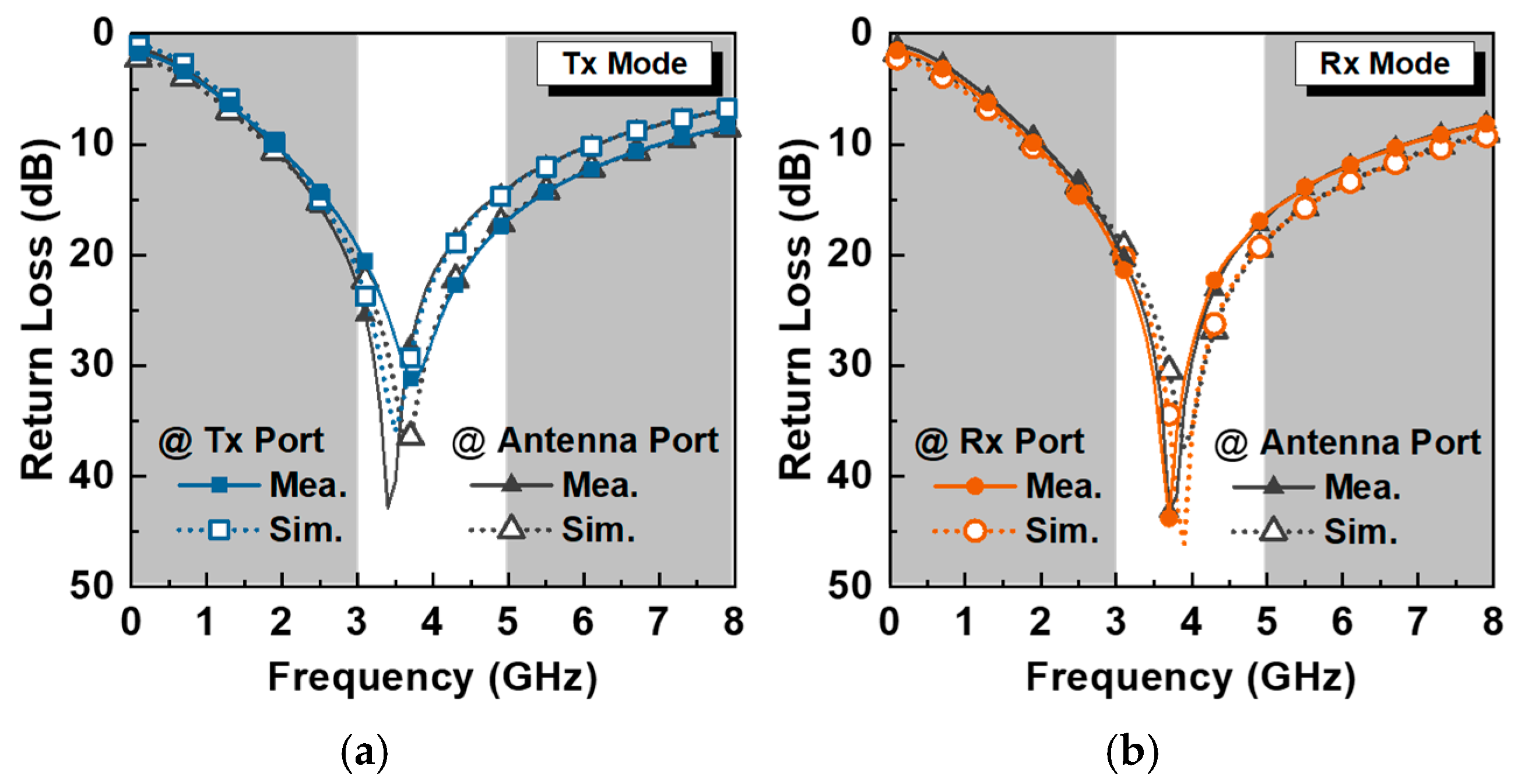
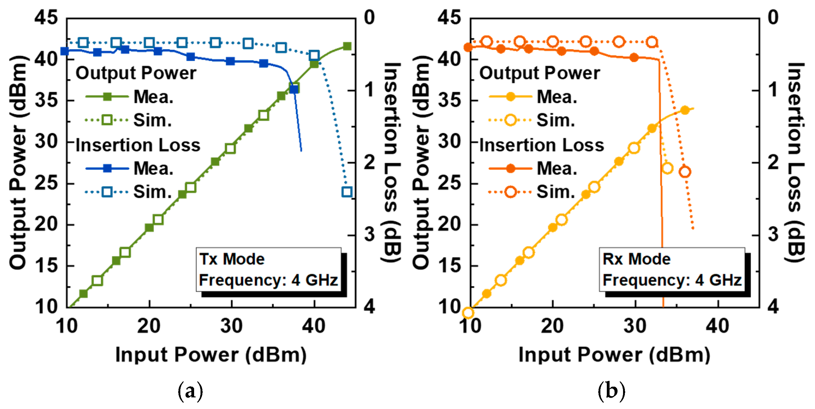
In order to verify the feasibility of the proposed switch to which the ESD protection technique is applied, a switch is fabricated using a 500 nm GaAs BiFET process. The 500 nm GaAs BiFET process provides HBT and pHEMT, and only pHEMT with a gate length of 500 nm is used for switch design. The operating frequency of the designed switch is set from 3 GHz to 5 GHz for application in the n77 and n79 bands.
The designed switch consists of a shunt inductor and four transistors as shown in Figure 3. Figure 5 shows the simulation results according to the frequency of the finally used transistors and LESD. Parasitic capacitances are extracted as capacitances between the drain and the source of the transistor when the transistor is in the off state. The LESD serves as an ESD protection device while also serving as an inductance of the parallel resonance circuit to prevent power loss. VC is designed to be 0 V and −8 V. The VC is applied to the gate through a resistor of 96 kΩ.
In an ideal case, LESD is commonly used in Tx and Rx mode operations, so CTS + CRX and CRS + CTX in (3) should be the same, resulting in fTX and fRX being the same. However, CTS + CRX and CRS + CTX can be formed somewhat differently because not only off-capacitance but also on-resistance should be considered when determining the transistor. In particular, the on-resistance of MRS and MTS directly affects isolation in Tx and Rx modes, respectively. In this study, for convenience, ILTX and ILRX, which are insertion losses in each mode, are defined as follows.
I L T X = 10 log P T X P A N T d B , I L R X = 10 log P A N T P R X d B
In ILTX, PTX is the power supplied from the Tx port, and PANT is the power delivered by the antenna port. Similarly, in ILRX, PANT is the power supplied from the antenna port, and PRX is the power delivered by the Rx port. Here, the PANT/PTX and PRX/PANT for the calculation of (4) may be calculated as follows.
f o r T x m o d e : P T X P A N T = 1 + j R L ω C E Q , T X 1 ω L E S D f o r R x m o d e : P A N T P R X = 1 + j R L ω C E Q , R X 1 ω L E S D
Here, RL is the terminal impedance at each port, and in this study, RL is assumed to be 50 Ω. In this study, the sizes of the transistors are determined to minimized the on-resistances of the transistors under the condition that both ILTX and ILRX are lower than 0.5 dB. For convenience of comparison, the simulation results of the designed switch are shown together with the measurement results in the next section.

3. Design Results

Figure 6 is a chip photograph of the fabricated switch. The overall chip size including test pads is 0.890 × 0.875 mm2. The control voltage is applied through a bonding wire, and the RF signal is measured using a GSG probe.
Because the interconnection lines and inductor, including the GSG pads, are all optimized through electromagnetic (EM) simulation, deterioration of simulation accuracy due to parasitic components of passive devices and metal lines is suppressed. As a result, in this study, the simulation results show high similarity to the measurement results. For convenience of comparison between the simulation and the measurement results, the simulation and the measurement results are provided together. Measurement is performed on three samples. The variation between samples is negligible. In addition, the power loss caused by GSG pads is included in the performance of the switch without de-embedding. On the other hand, power loss due to RF cables and connectors for measurement is carefully de-embedded.
Figure 7 shows the return losses. At 3 GHz to 5 GHz, the measured return losses are greater than 14.0 dB and 16.2 dB in the Tx and Rx modes, respectively.
As shown in Figure 8, the measured insertion losses are less than 0.35 dB and 0.32 dB in the Tx and Rx modes, respectively. In particular, because both Tx and Rx modes can be equalized with parallel resonance circuits including LESD, the Tx and Rx modes showed similar measurement results. Isolations are measured higher than 31.6 dB and 33.9 dB in the Tx and Rx modes, respectively.
As shown in Figure 9, the output power according to the input power is measured at the center frequency of 4 GHz. The linearity of the Tx mode is measured relatively higher than that of the Rx mode. The measured input 1 dB compression points (IP1dBs) at 4 GHz are 38.0 dBm and 33.0 dBm in Tx and Rx modes, respectively.
Table 1 shows the performance comparison of GaAs switches with an operating frequency of Sub-6 GHz. In Table 1, in the case of commercial products, because the performance is in the package state, the power loss by the package is included in the insertion loss. The performances of the proposed switch in the range of 3 GHz to 6 GHz as well as 3 GHz to 5 GHz, which is the target frequency, are also provided in Table 1. It can be seen that the switch in this study shows reasonable performance even though a shunt inductor for ESD protection is used.
In this study, the proposed ESD protection technique was applied to the GaAs pHEMT switch for Sub-6 GHz applications. However, the proposed ESD protection technique using a shunt inductor can be easily applied to switches connected external antennas regardless of operating frequency and power handling capability. In particular, the proposed switch structure may also benefit emerging applications such as microwave sensing and non-contact detection [24,25].

4. Conclusions

In this study, we proposed an ESD protection technique of a switch constituting the RF FEM. For this, a shunt inductor was provided in the antenna port of the switch. In order to suppress the performance degradation caused by the shunt inductor, the inductor was co-designed with the matching network of the switch. Therefore, the shunt inductor serves as an ESD protection device while also serving as a component of a parallel resonance circuit to minimize the insertion loss of the switch. In addition, in order to secure power handling capabilities, transistors turned off in the Tx mode were designed as quadruple-gate transistors. The proposed switch was fabricated with GaAs pHEMT provided in the 500 nm GaAs BiFET process. For frequencies from 3 GHz to 5 GHz, the measured insertion losses were lower than 0.35 dB and 0.32 dB in the Tx and Rx modes, respectively. The measured isolations were higher than 31.6 dB and 33.9 dB in the Tx and Rx modes, respectively. The IP1dB of the Tx mode was measured as 38.0 dBm at the operating frequency of 4 GHz.

Author Contributions

Conceptualization, J.K., J.L., T.K. and C.P.; methodology, J.K., J.Y. and C.P.; investigation, J.K.; supervision, C.P.; writing—original draft, J.K.; review and editing C.P. All authors have read and agreed to the published version of the manuscript.

Funding

This work was supported by the Soongsil University Fund of 2022.

Data Availability Statement

All the material conducted in the study is mentioned in article.

Conflicts of Interest

The authors declare no conflicts of interest.

References

  1. Takenaka, K.; Noguchi, Y.; Arayashiki, S.; Wada, T. Load-Modulated Balanced Amplifier Design for Handset Applications. IEEE Microw. Wirel. Technol. Lett. 2023, 33, 855–858. [Google Scholar] [CrossRef]
  2. Kong, M.; Wu, Y.; Wang, W. The Co-Design of Broadband Diplexer and Quasi-Reflectionless Lowpass/Highpass TFIPD Filter Chip. IEEE Trans. Circuits Syst. II-Express Briefs 2023, 70, 486–490. [Google Scholar] [CrossRef]
  3. Bo, S.F.; Ou, J.-H.; Peng, Y.J.; Xuan, K.; Xu, J.-X.; Zhang, X.Y. Broadband GaAs HBT Doherty Power Amplifier for 5G NR Mobile Handset. IEEE Trans. Circuits Syst. II-Express Briefs 2024, 71, 527–531. [Google Scholar] [CrossRef]
  4. Ariturk, G.; Almuqati, N.R.; Yu, Y.; Yen, E.T.-T.; Fruehling, A.; Sigmarsson, H.H. Exact Synthesis of Hybrid Acoustic-Electromagnetic Filters with Wideband Chebyshev Responses. IEEE Trans. Microw. Theory Tech. 2024, 72, 3185–3199. [Google Scholar] [CrossRef]
  5. Kim, D.; Im, D. A 2.4 GHz Reconfigurable Cascode/Folded-Cascode Inductive Source Degenerated LNA with Enhanced OP1dB and OIP3 over Gain Reduction. IEEE Trans. Circuits Syst. II-Express Briefs 2023, 70, 1831–1835. [Google Scholar] [CrossRef]
  6. Yang, F.; Zhang, B.; Song, L.; Xu, Y. A Compact RF Front-End SiP with Improved Harmonic Suppression for Dual Polarization Phased Array Radar. IEEE Microw. Wirel. Technol. Lett. 2024, 34, 350–353. [Google Scholar] [CrossRef]
  7. Lee, S.; Seo, W.; Kim, S.; Ko, B.; Lee, S.; Kim, M.-S.; Kim, J. A Concurrent 26/48 GHz Low-Noise Amplifier with an Optimal Dual-Band Noise Matching Method Using GaAs 0.15 μm pHEMT. IEEE Trans. Circuits Syst. II-Express Briefs 2024, 3, 1096–1100. [Google Scholar] [CrossRef]
  8. Park, J.; Lee, S.; Hong, S. A 24–40 GHz Differential SPDT Switch with an NMOS and PMOS Alternating Structure and Leakage-Canceling Capacitors. IEEE Trans. Circuits Syst. II-Express Briefs 2023, 70, 86–90. [Google Scholar] [CrossRef]
  9. Lin, Y.-S.; Lan, K.-S.; Chen, B.-S. Wideband Millimeter-Wave Power Divider and SPDT Switch Using Inverting Spiral-Coupled-Line. IEEE Trans. Circuits Syst. II-Express Briefs 2023, 70, 1575–1579. [Google Scholar] [CrossRef]
  10. Lee, S.; Park, J.; Hong, S. W-Band Compact Balun-Embedded SPDT Switch with Leakage-Canceled Overlapped Transformers. IEEE Microw. Wireless Technol. Lett. 2023, 33, 1532–1535. [Google Scholar] [CrossRef]
  11. Ma, G.; Yang, Z.; Meng, F. An Ultracompact Frequency-Reconfigurable SPDT Switch with 42-dB Isolation. IEEE Microw. Wirel. Technol. Lett. 2024, 34, 45–48. [Google Scholar] [CrossRef]
  12. Kwon, J.; Lee, J.; Kim, T.; Seo, D.; Yoo, J.; Cho, J.; Park, C. Asymmetric SOI CMOS Switch with Series and Parallel Resonators to Enhance Isolation. IEEE Trans. Circuits Syst. II-Express Briefs 2024, 71, 1964–1968. [Google Scholar] [CrossRef]
  13. Jang, S.; Kong, S.; Lee, H.-D.; Park, J.; Kim, K.-S.; Park, B. A 28 GHz >30 dBm Output P1dB SPDT switch with integrated ESD protection in CMOS 65 nm. In Proceedings of the 2020 50th European Microwave Conference (EuMC), Utrecht, The Netherlands, 12–14 January 2021; pp. 140–143. [Google Scholar]
  14. Hao, W.; Di, M.; Pan, Z.; Li, X.; Miao, R.; Cahoon, N.; Wang, A. A 60GHz Traveling-Wave SPDT Switch with HBM and CDM ESD Protection in 45nm SOI CMOS. In Proceedings of the 2022 IEEE 16th International Conference on Solid-State & Integrated Circuit Technology (ICSICT), Nangjing, China, 25–28 October 2022; pp. 1–4. [Google Scholar]
  15. Ker, M.-D.; Chou, C.-I.; Lee, C.-M. A novel LC-tank ESD protection design for Giga-Hz RF circuits. In Proceedings of the IEEE Radio Frequency Integrated Circuits (RFIC) Symposium, Philadelphia, PA, USA, 9–10 June 2003; pp. 115–118. [Google Scholar]
  16. Lin, C.-Y.; Chu, L.-W.; Tasi, S.-Y.; Ker, M.-D.; Lu, T.-H.; Hsu, T.-L.; Hung, P.-F.; Song, M.-H.; Tseng, J.-C.; Chang, T.-H.; et al. Modified LC-tank ESD protection design for 60-GHz RF applications. In Proceedings of the 2011 20th European Conference on Circuit Theory and Design (ECCTD), Linköping, Sweden, 29–31 August 2011; pp. 57–60. [Google Scholar]
  17. Park, C.-K.; Kim, M.-G.; Kim, C.-H.; Hong, S. Ku-band low noise amplifier with using short-stub ESD protection. In Proceedings of the IEEE Radio Frequency Integrated Circuits (RFIC) Symposium, Philadelphia, PA, USA, 9–10 June 2003; pp. 671–674. [Google Scholar] [CrossRef]
  18. Yoon, J.; Park, C. 5-GHz low noise amplifier with ESD protection method using transformer. Microw. Opt. Technol. Lett. 2014, 56, 684–689. [Google Scholar] [CrossRef]
  19. CG2185X2: 6GHz Medium Power SPDT Switch; CEL: Santa Clara, CA, USA, August 2017.
  20. TQP4M0008: Low Loss Reflective SPDT Switch; Qorvo: Greensboro, CA, USA, June 2018.
  21. SKY13320-374LFM: 0.1–6.0 GHz GaAs SPDT Switch; Skyworks: Irvine, CA, USA, January 2018.
  22. Kwon, J.; Yoo, J.; Lee, J.; Kim, T.; Park, C. Sub-6 GHz GaAs pHEMT SPDT switch with low insertion loss and high power handling capability using dual-gate technique. In Proceedings of the IEEE Wireless and Microwave Technology Conference (WAMICON), Melbourne, FL, USA, 17–18 April 2023; pp. 49–52. [Google Scholar]
  23. Lee, J.-E.; Song, J.-H.; Baek, M.-S.; Son, J.-T.; Kim, J.-H.; Lee, E.-G.; Choi, S.; Kim, C.-Y. A Sub-6 GHz Asymmetric GaAs SPDT Switch with High Tx-to-Rx Isolation and Low Insertion Loss. IEEE Microw. Wirel. Technol. Lett. 2024, 34, 490–492. [Google Scholar] [CrossRef]
  24. Ali, L.; Wang, G.; Meng, F.; Ding, X.; Adhikari, K.K.; Wang, C. MXene-Coated Planar Microwave Resonator Sensor for Ultrasensitive Humidity Monitoring. IEEE Microw. Wirel. Technol. Lett. 2023, 33, 1572–1575. [Google Scholar] [CrossRef]
  25. Wang, S.; Wan, C.; Zheng, Y. Microwave Characterization of Glucose Level Using Composite PMS-HMSIW Cavity Resonator Integrated with Microfluidic Channel. IEEE Trans. Instrum. Meas. 2024, 73, 6009116. [Google Scholar] [CrossRef]
Figure 1. Conceptual block diagram of FEM with ESD protection solution.
Electronics 14 01707 g001
Figure 2. Human body model of ESD with shunt inductor: (a) schematic and (b) frequency response.
Electronics 14 01707 g002
Figure 3. Proposed SPDT switch with ESD protection using a shunt inductor.
Electronics 14 01707 g003
Figure 4. Equivalent circuits for (a) Tx mode and (b) Rx mode.
Electronics 14 01707 g004
Figure 5. Characteristics of the used devices: (a) transistors and (b) LESD.
Electronics 14 01707 g005
Figure 6. Chip photograph of the designed GaAs SPDT switch.
Electronics 14 01707 g006
Figure 7. Design results of return loss: (a) Tx mode and (b) Rx mode.
Electronics 14 01707 g007
Figure 8. Design results of (a) insertion loss and (b) isolation.
Electronics 14 01707 g008
Figure 9. Design results of power handling capability: (a) Tx mode and (b) Rx mode.
Electronics 14 01707 g009
Table 1. Performance summary and comparison of GaAs SPDT switches operating at sub-6GHz.
ReferenceTech.Freq. (GHz)Fractional Bandwidth (%)Return Loss (dB)Insertion Loss (dB)Isolation (dB)IP1dB (dBm)Chip Size (mm2)
TxRxTxRxTxRxTxRx
CEL’17
[19]
GaAs2–6100>18<0.4>2632 @ 6 GHz-
Qorvo’18
[20]
GaAs0.1–6193>15<0.85>1735 @ 3 GHz-
Skyworks’18
[21]
GaAs0.1–6193>20<0.6>2434 @ 2.45 GHz-
WAMICON’23
[22]
500 nm GaAs3–550>15<0.3>32.7>34.2 @ 3 GHz0.83
MWTL’24
[23]
500 nm GaAs3.3–541>15.8<0.53<0.39>36.4>25.4>40 (1)-0.84
This work500 nm GaAs3–550>14.0>16.2<0.35<0.32>31.6>33.938.0 (1)33.0 (1)0.78
3–666.7>10.3>12.2<0.62<0.46>28.5>30.2
(1) @ 4 GHz.
Disclaimer/Publisher’s Note: The statements, opinions and data contained in all publications are solely those of the individual author(s) and contributor(s) and not of MDPI and/or the editor(s). MDPI and/or the editor(s) disclaim responsibility for any injury to people or property resulting from any ideas, methods, instructions or products referred to in the content.

