1. Introduction
The study of negative feedback with amplifiers is usually introduced by following different strategies, some of them focusing on theoretical principles, and others emphasizing practical circuit applications.
The most common methods are the “two-port network” analysis, the “return-ratio” approach, and the “cut-insertion” method. The “two-port network” analysis [
1,
2,
3,
4,
5,
6,
7,
8,
9,
10,
11,
12] is the simplest and most intuitive one, often used as as introduction to the other methods. An example of its implementation to a common circuit with negative feedback is depicted in
Figure 1. In short, the amplifier is considered to have infinite input impedance and zero output impedance. In this way, the analysis of the circuit in
Figure 1 is quite simple and leads to
The result allows us to highlight the essential properties of the feedback amplifier theory; however, due to the previous approximations (
input/output impedances), the gain expression (
1) does not include the connected source and load resistances (
and
), which are always present in a real case scenario. Frequency behavior (and stability) is studied only when the frequency dependence of the feedback block
and amplifier gain
A are explicit. Furthermore, in (
1) the factor
must be dimensionless, but there are some cases—which will be explored in the following sections—where
is a non-dimensionless quantity, leading to some uncertainty in the meaning of
A, which would also need to be a dimensional quantity.
A second common approach, the “return-ratio” analysis, describes the network in its entirety and requires the construction of a circuit sub-model or applying strict mnemonic rules [
13,
14,
15,
16,
17,
18]. The illustration shown in
Figure 2 is often adopted to introduce the “return-ratio” approach. The
block again represents the feedback path, and the
block is the direct transmission of the signal from the input to the output due to the non-ideality of both the
block and the amplifier.
When the amplifier is ideal, the solution of
Figure 2 turns out to be
In the above result, the loop gain
can take a more complex expression if the amplifier is not ideal. The blocks
and
must be correctly identified and extracted from the real circuit by following specific rules.
The “return-ratio” approach can also be exploited to determine the input and output impedances of the network with feedback using Blackman’s theorem (BTH in the following) [
19].
The “return-ratio” technique is able to provide an accurate description of the network. Still, the procedure requires careful application since the topology of the actual circuit needs to be simplified to match the model illustrated in
Figure 2. To aid this process, several educational examples are typically provided and used as a reference [
13,
14,
15,
16,
17,
18].
The third most common approach relies on the “cut-insertion” method [
20], which requires some experience in the selection of the cut point in order not to change the network properties. Recently, this method has been greatly enhanced and generalized [
21,
22,
23], although requiring further experience and knowledge of circuit theory, thus not easily accessible by inexperienced users.
In this paper, we will focus on a fourth method for feedback network analysis, based on the so-called Asymptotic Gain Formula (AGF) or Rosenstark method [
15,
24,
25]. This method has the main advantage that does not require sub-modeling the circuit topology to characterize the network fully. The amplifier network is not modified and is studied by following a few steps in which infinite-gain, zero-gain, and zero-applied-signal cases are used to extract the necessary parameters, including input and output impedances. This allows also complex networks, like amplifiers with multiple feedback loops, to be easily analyzed without making further assumptions.
The original formulation of the Rosenstark method relied on the BTH [
19] for the evaluation of the input and output impedances. BTH, however, often requires further procedures and calculations to derive the loop gains with shorted or open-circuited inputs.
In the following, we will show that, by extending the application of AGF to the calculation of input and output impedances, no further calculations of the loop gain are needed, and input and output impedances can be obtained easily, exploiting the fact that every node and branch of the network is subject to feedback. Starting from our method, Blackman’s theorem proof is also obtained directly and interpreted from a different viewpoint.
The analysis of feedback in amplifiers using our approach is particularly suitable for those unfamiliar with circuit analysis, such as undergraduate engineers or experimental physics students who do not have a dedicated background in circuit design. The use of AGF and the proposed method is also convenient for studying electrical parameters other than gain and input/output impedances within the amplifying network, like noise.
In
Section 2, we begin by refreshing the Rosenstark method with the help of a practical example. Next, in
Section 3, we demonstrate how this method can be extended to efficiently compute the input and output impedances of the network, eliminating additional steps required by the BTH.
Section 4 presents practical applications of our extension, starting from simpler circuits (inverting amplifier in
Section 4.1, and a current amplifier in
Section 4.2), then moving to more complex ones like the transconductance amplifier (
Section 4.3) and a dual feedback circuit (
Section 4.4). The example of the transconductance amplifier also includes a numerical comparison with other methods from the literature. In
Section 5, we apply the same method to noise evaluation, illustrating its versatility in analyzing any generic network parameter. Finally, in
Section 6, we discuss the advantages and the drawback of the proposed method in comparison to the others presented in the introduction.
MATLAB scripts (version R2023b) containing the calculations performed in the examples are provided as
Supplemental Material.
2. General Solution of a Feedback Amplifier with the Rosenstark Method
The derivation of AGF with the Rosenstark method is briefly refreshed here, as it will be exploited in the rest of the paper. The procedure starts from a generic circuit, like the one shown in
Figure 3. The amplifier is modeled with finite input (
) and output (
) impedances. The load impedance at the output (
) and the source impedance at the input (
) are also considered.
We begin our analysis from the boundary condition consisting of an extremely high amplifier gain, close to
∞. In this case, the output signal has a finite value only if the difference between the inputs (
and
) is close to 0 V and, consequently, the current flowing through
is also 0 A. Regardless of the components that are present, we therefore obtain
In a real situation, the gain
A is not
∞, and it decreases at high frequencies. In order to describe the behavior of the real network beyond the boundary condition (
3), we have to solve the circuit shown in
Figure 3, trying to exploit the result obtained in (
3). We write the system of equations as if we did not know that a feedback path was present:
The AGF is an elegant way of interpreting the system (
4) from both an algebraic and a physical point of view. We start solving the first equations and omit the last one, the one that connects the input to the output (the “linking” equation in the following). This is equivalent to considering
a temporary independent variable or replacing the dependent voltage source
in
Figure 3 with a test signal. By doing so, we can write respectively
and
as functions of
and
, as shown in (
5). The circuit in
Figure 3 has no particular properties that stand out with respect to other networks, so the solution of a generic circuit will involve more or fewer equations, depending on the complexity of the network. The achieved generic solution can be written as follows:
where
a,
b,
c, and
d are the results of the solution of system (
4), “linking” equation excluded, or of any other generic network. These results will depend on all the components present in the network, which can be resistors, as in
Figure 3, capacitors, or inductors. We must now consider the “linking” equation,
, that allows us to write
as a function of the input source
alone:
We now use the result obtained by studying the boundary condition (
3):
where the limit in the last line of (
7) is valid since
a,
b,
c, and
d do not depend on
A.
Substituting the last result of (
7) in (
6) gives the following result:
Now, we redefine the term
a as
, which should be negative to obtain a negative feedback, the term
d as
, and introduce the loop gain
T as
. Then,
The combination of the boundary condition and the “linking” equation leads to the final result obtained above, which is valid for any feedback network. In doing so, we have obtained the same result from the “return-ratio” approach, shown in (
2), without the need to reshape or extract a sub-model from the network.
To summarize, with the Rosenstark method the network can be studied by writing down a reduced system of equations and by applying the superposition principle, as is done with a system of linear equations [
24,
25]. The advantage of AGF (
9) is that the method to get to the solution is the same for every feedback network.
The procedure that needs to be followed to obtain the parameters of interest in (
9) can be summarized in the following list:
The above recipe is designed for the case of a differential voltage amplifier but remains valid for current amplifiers and hybrid amplifiers that combine currents and voltages at their inputs and outputs. It is also suitable for single-ended or differential amplifiers, provided the appropriate variables in (10) are used.
Very often, when using a large-gain operational amplifier, the contribution of direct transmission is negligible, and the corresponding equation for evaluating it in (10c) can be omitted, further simplifying the procedure.
The amplifier is completely modeled with all its parameters, including the input and output impedances as shown in the next section.
When , the gain is close to . Hence, if is less than 1, the resulting gain will be greater than 1, while, if is greater than 1, the output signal is attenuated with respect to the input. This last case is what happens when input and output impedances are evaluated, as shown later.
When there is no feedback on the amplifier, then , and both and T are also equal to 0. The only contribution to the gain in this case is the one coming from the amplifier in open-loop operation. The same effect occurs when T decreases with frequency: the loop gain becomes smaller than 1 and the gain in closed-loop operation is reduced to that of the amplifier.
As shown, the procedure does not need to introduce new circuital sub-models and allows computing any type of parameter within the network, whether it is attenuated or amplified. Multiple-feedback amplifiers are also managed naturally, since this method does not require identifying the signal loop.
Another important property of the AGF is that the nodes chosen as inputs or outputs, like the ones in the example of
Figure 3, have no particular attribute and could be any node of the network. In the system of Equation (
5), based on the superposition principle, the parameter
is independent of the point at which a voltage or current source is applied to the network, provided that the topology is not affected. This means that, regardless of the feedback node under consideration and the location of the source, the loop gain
T remains the same, since it is a feature of the network itself. Consequently, any parameter can be characterized with the same procedure (10). The next section, dedicated to the characterization of input and output impedances, fully exploits this property and provides an example of its application.
3. Input and Output Impedances of Amplifiers with Feedback
The input and output impedances of feedback amplifiers can be evaluated using various methods [
14,
26,
27,
28,
29,
30,
31]. Among them, the one developed by Blackman [
19] (BTH) is the most immediate to apply and the most widely used after having analyzed the network with the AGF shown in the previous section.
The Blackman theorem states that the impedance seen from a node (for example from the source
of
Figure 4,
) is
The impedance
is equal to the impedance when the amplifier is switched off,
, multiplied by a ratio that includes the loop gain
obtained with input shorted (
), and the loop gain
is obtained with input open (
). New calculations are thus required.
As AGF allows to determine the gain of the feedback network, the BTH allows one to calculate input and output impedances in an unambiguous way. However, other network characteristics are also interesting to the designer, with noise being a notable one.
In the following, we propose an alternative and simple method to obtain input and output impedances, which can also be easily extended to any other network parameter, such as noise, as shown later. The method makes use of the AGF only, or the procedure shown in (10). In addition, this finds a direct correspondence with the laboratory characterization of the real network.
The proposed procedure is based on the property that all nodes of the network have equivalent features: the nodes to which the signals are applied and in which the resulting effects are read can be any. We now use this property for the input impedance evaluation of the circuit in
Figure 4.
To obtain
, as already stated, we need to evaluate the ratio between the input signal
and its generated current
. This current is the same current that flows through
, also known as
. With
being a current that flows in a branch of our feedback network, it is subjected to the feedback action, and (10d) can be applied in the same way it was used to obtain the gain of the network:
where
,
, and
T are evaluated according to the solution of Equations (10a)–(10c). We have to bear in mind that the loop gain
T is the same for all nodes and branches, and has to be evaluated only once, provided that the network topology is not altered.
and
, on the contrary, need to be re-evaluated, since they are dependant on which inputs and outputs nodes are considered.
If we consider
in
Figure 4, we have that
, so the current
through
is zero and, consequently,
. Under ideal conditions (
),
is strongly attenuated and therefore the input impedance, being equal to
, is
∞. Put differently, the only contribution to
is given by the direct transmission term, as it can be extrapolated from Equation (12).
is the impedance evaluated when
:
Thus,
is the inverse of the input impedance measured under open-loop conditions,
.
Finally, combining everything in (12),
In conclusion,
The impedance
in (15) is the same as the one obtained in other references [
16,
19,
30,
31] or from the BTH, when considering the fact that
for the specific case of
Figure 4. In particular, this result is the classical one for the voltage-series case, where the input impedance can be evaluated by multiplying the open-loop input impedance by
.
We believe the proposed procedure (10) is advantageous as it allows the impedance to be uniquely evaluated, regardless of the type of test signal adopted, either a voltage or current signal. We will see more practical examples in the next section.
The BTH is also easily proved by starting from (12) and collecting
:
Then we obtain
The BTH (11) is then proved if we consider that
The measurement of the output impedance
is performed by referring to
Figure 5. This time, we apply a test current signal
to the output node, as if we were in the laboratory studying a real circuit. The input excitation
is, of course, turned off. We now apply (10d) to
Figure 5, choosing
as the feedback variable:
Again, T remains unchanged since the test signal does not alter the network topology.
is derived by applying (10a) (
) to
Figure 5 and, in this case,
results in
; consequently, the currents in
and
are zero and so is
. As a consequence,
and the first term in (19) is negligible.
is found with (10c), or
, and results in
where
is the impedance measured under open-loop conditions.
Then, inserting all the results in (19),
and the output impedance is
Again, this is the canonical conclusion whenever a voltage is amplified in a feedback network.
4. Examples of Input and Output Impedance Evaluation
4.1. The Inverting Amplifier
The typical configuration of an inverting amplifier is shown in
Figure 6. For its analysis, we start again from (10a). Considering
, we obtain
This last result suggests a way to figure out what kind of variable, either a voltage or a current, is amplified and generated at the output: the preferred variables are those that lead the output node to being not dependent on the source (
) and the load (
) impedances. In Equation (23), by considering
as the sourcing input, the output node is dependent on the source impedance
, meaning that the amplifier input is sensitive to current rather than voltage. Another effect is about the input impedance, as we will verify below.
To continue the analysis, we must solve Equations (10b) and (10c) by first setting
and then
to obtain
and
, respectively. For the circuit configuration of
Figure 6 this results in
Finally,
The output impedance of the network is easily evaluated using the test circuit in
Figure 7, similarly to what then resulted in (22) from the network in
Figure 5:
The evaluation of the input impedance of the inverting configuration in
Figure 6, on the contrary, leads more often to erroneous conclusions, since the impedance seen from the source
can be mistakenly identified as the sum of
and the other contributions to the open-loop input impedance, all divided by
. This, however, is not the case, as the input impedance depends on whether the sourcing input is a current or a voltage. With the proposed method, any erroneous analysis can be completely avoided.
The input impedance
, as seen from the input voltage source
shown in
Figure 6, is given by the ratio
, and
, being split between
and
, also flows in the feedback loop. Writing Equation (10c) for the network, we have
With , we have and .
is obtained by setting
:
The result tells us that the impedance seen by is close to , especially if .
On the other hand, if the signal is a current source
as in
Figure 8, we can write (10c) choosing
as the feedback variable (
is zero for this case):
and the input impedance
seen by the current source results in
It is interesting to highlight that the general expressions of
(31) and
(29) can assume a simpler form if we consider
as given by the parallel combination of
and and impedance
, as shown in
Figure 8, such that
then requires some further manipulation:
It is worth noting that the loop gain T within is not the same as in (24) but has to be evaluated with .
By looking at (27) and (30), which resulted in (29) and (31), respectively, we can obtain a hint on what to expect for the impedance expression, either input or output. If the feedback signal generated by the test source includes only a single term proportional to (i.e., is zero), then the measured open-loop impedance at the input or output is multiplied or divided by . This is the case of (30) and (31). Otherwise, a more elaborated dependence is expected, as in (27) and (29).
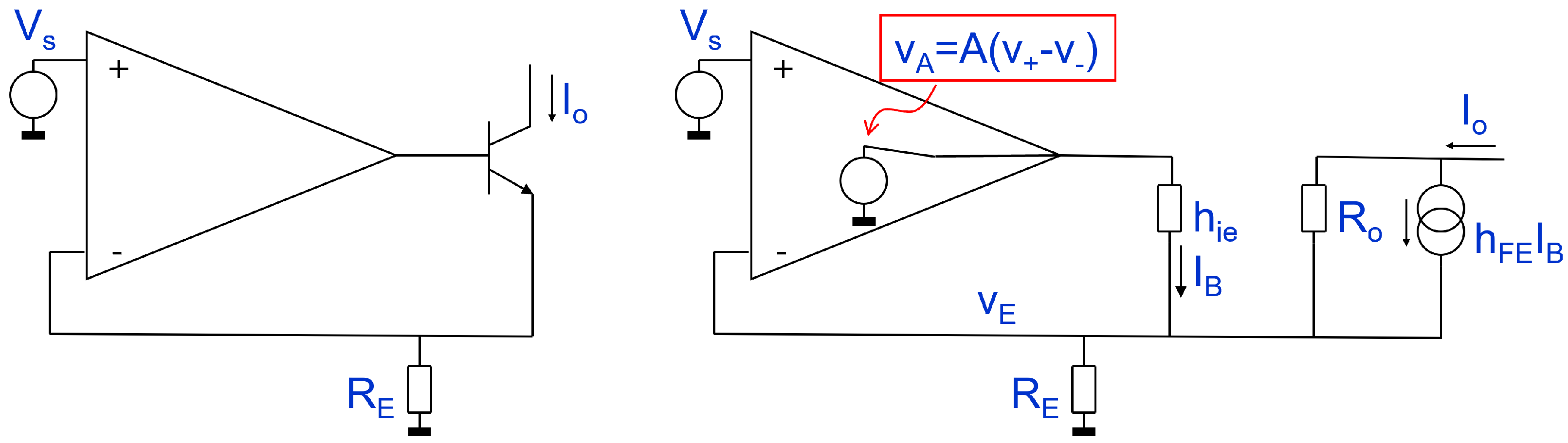
4.2. A Current Amplifier
In this further example, we study the output impedance of the circuit of
Figure 9, a current amplifier. From (10a), assuming
, we first obtain
which results in
We see that the output current is proportional to the input current and does not depend on source or load impedances ( and ), justifying the assumption that the circuit is a current amplifier.
To simplify, let us consider the loop gain T to be already evaluated from (10b).
The output impedance with test voltage
and feedback current
is then found by solving the network shown in
Figure 10:
With , the node is zero; therefore, the current in and is also zero. This in turn forces the current through to be zero; consequently, is also zero, finally determining the current through , i.e., , to be zero as well, and thus .
is calculated in the following:
Thus,
In conclusion,
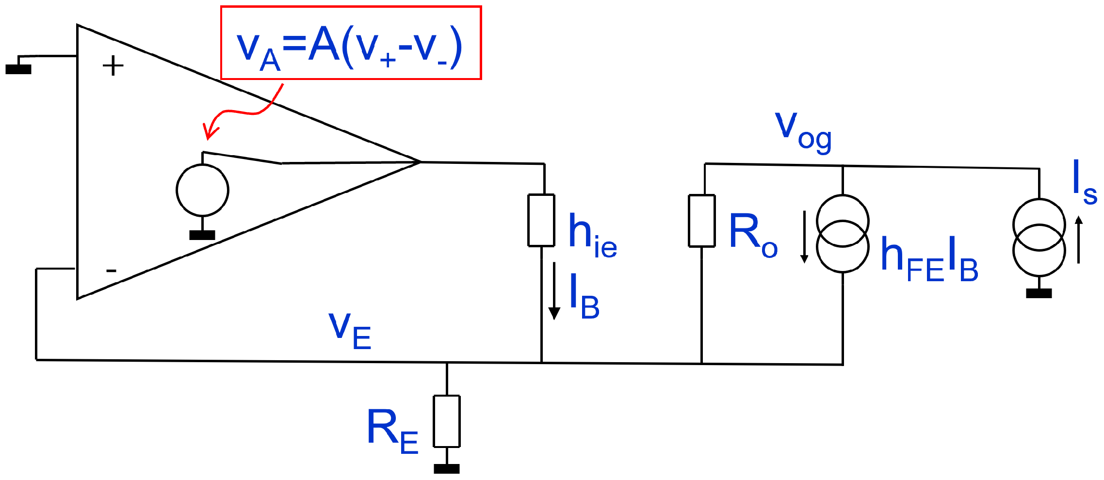
Let us now change perspective and measure the output impedance
using a current generator as the test signal, as in
Figure 11. The feedback variable is the current
that flows in
. If
, then
turns out to be zero, and the current trough
is also zero and
. This implies that the current trough
is equal to
and
. The direct transmission term
is calculated setting
, which results in the following system:
from which
Namely,
The output impedance
now results:
where
satisfies
Again, the procedure emphasizes that impedances cannot be given a pre-defined form, except in certain cases where
, and suggests a simple method for evaluating them. In
Figure 10, the impedance is measured with a test voltage source put in series with the load impedance
, which in turn results in series with the output impedance, while in
Figure 11, the measurement is made with a test current source put in parallel with the load impedance
, which results in parallel with the output impedance. In this last example, we applied a test current and evaluated a current, rather than a voltage, simply because we found it easier. The application of the AGF gives this flexibility.
4.3. A Transconductance Amplifier
In the following example, we consider the same transconductance amplifier analyzed in [
21,
30], also shown in
Figure 12. To ease calculations, the operational amplifier can be considered as ideal (infinite input impedance and zero output impedance). The results obtained will allow a numerical comparison with the other common methods used in the references above (“two-port network” analysis for [
30] and “cut-insertion” method for [
21]).
Let us again assume that the loop gain
T has been already evaluated from (10b) for the circuit in
Figure 12 with a large load impedance
:
The output impedance is calculated according to the circuit in
Figure 13, with test current
and feedback voltage
, using the usual Equation (10d):
The term
is obtained by considering the case with
, thus
. The equations at the nodes give
The direct term is evaluated switching off the amplifier (
) and solving the following system:
Finally, by combining (45), (47), and (48) into (46), we can compute the exact output impedance:
The rightmost term vanishes if
, and, as expected, the output impedance is exactly
. Considering the parameter values also used in [
21,
30] (
,
= 5 k
,
= 50 k
,
,
), the output impedance is 5049.75 k
. This result is in perfect agreement with SPICE tools and with the “cut-insertion” method of [
21], and 11% more precise than the “two-port network” analysis in [
30], confirming the accuracy of the proposed method.
4.4. Dual Feedback Amplifier
Dual or multiple feedback amplifiers are usually studied by considering how the feedback loops are positioned. The analysis is often performed with approximations or sub-models [
17,
32,
33,
34,
35]. The AGF method (10), instead, does not require any change to the network or knowledge of the number of feedback loops present in the network to assess the parameters of interest.
An example is shown in
Figure 14. The first feedback loop goes from the output to the inverting input and can be regulated with resistors
and
. The second feedback loop inverts the output signal
and feeds it to the non-inverting input through resistor
.
As usual, we start our analysis using procedure (10) and no other hypothesis. The closed-loop feedback is found with
, from (10a), which we know results in
:
from which we obtain
The loop gain,
, is evaluated when
, (10b):
The loop gain expression is rather long, so we will report here only the approximated result with
and
:
The direct transmission term,
, is obtained when
, (10c):
With the same approximations (
and
), the solution is the following:
Now (51), (53), and (55) allow us to write
as
The result has been obtained without any assumptions on the number or topology of feedback loops. The evaluation of input and output impedances follows the same approach.
For the input impedance, we are interested in the feedback variable
, as shown in
Figure 14. We first evaluate it for the case
:
Using an expression for
borrowed from the system (50) and its solution (51), we obtain
The direct transmission term through
can be evaluated when
. Again, we exploit system (54) to extract an expression for
:
Putting together (58) and (59) with
,
Finally, substituting
from (53) into (60) leads to
This result tells us that, if the feedback from were not present, namely , the input impedance would become large, which is an expected outcome for a voltage amplifier, whereas, if feedback from both and were removed, setting for instance, the input impedance of the amplifier alone would be small, as would happen if we were dealing with a current amplifier.
Once again, we emphasize that all the results were obtained with no modifications to the circuit. Dealing easily with dual feedback topologies is particularly helpful in the presence of parasitic elements that could enable other feedback paths apart from the main one.
5. Noise Characterization
In the last section of the paper, we will show that the proposed method can be applied very conveniently also for the noise characterization of a network.
The method consists of calculating the loop gain of the circuit, as always. After that, the output voltage corresponding to each noise source can be evaluated, as if calculating transfer functions. Different noise sources can then be superimposed quadratically at the output, or referred to other nodes (the input node, typically) dividing by the proper input-to-output transfer function.
As an example, we will evaluate the effect of a series noise source
at the input of the second stage of the two-stage feedback amplifier depicted in
Figure 15. To simplify the discussion, amplifiers
A and
B are supposed to have infinite input impedance and zero output impedance. We apply (10b) to the dependent source at the output of amplifier
A (
) and we find out the loop gain
T:
We set
and apply (10d) to
, considering noise
as the source:
From (10a) and
, we obtain
, which results in a zero current flowing in both
and
, and finally
and
. From (10c) and
, we obtain
, then
, and finally,
. Equation (63) becomes
An alternative approach would be applying the same procedure to amplifier B. The loop gain
T is thus evaluated by exploiting a dependent source
connected to the output of amplifier B:
The loop gain
T remains unchanged, as expected.
Equation (10d) now becomes
In this case, if
, then the output
is also zero and
, while if
, then
,
, and
:
Thus (66) reduces to
Equations (64) and (68) are exactly the same, as expected, although obtained starting the computation from two different points of the network.
Finally, we want to compute the input-referred noise
, i.e., the input noise source in series to
that generates the same effective output noise as
. We consider transfer function
to
, where the direct transmission is zero because the amplifiers are ideal:
By equalling
from this equation with either (68) or (64), we obtain
:
This shows that, in a multistage amplifier, the noise contribution of any stage is divided by the product of the gain of the previous stages in the chain, regardless of the presence and/or amount of feedback.
6. Discussion: Advantages and Limitations
In the previous sections, the proposed extension of the Rosenstark method has been comprehensively described, with the additional help of examples from practical circuits.
The clear advantage over the “two-port network” and “return-ratio” approaches is that there is no need to identify the network topology (series/shunt) or use sub-circuits to simplify the real case. Real-world applications with parasitic elements or complex networks, like those with dual feedback and other more exotic solutions that cannot be easily reduced to a simpler case, are more naturally solved with the proposed method. The results provided are exact, and the procedure to obtain them is unambiguous.
Our method can be also compared to the “cut-insertion” approach, which, together with its generalizations, provide the same exact results, as shown in the example of the transconductance amplifier in
Section 4.3, at the expense of being less straightforward than the set of procedures (10) shown in this paper.
One of the main limitations of the Rosenstark method, which our extension also inherits, is that it allows little insight into the increasing and decreasing of input and output impedances due to feedback. In the traditional “two-port network” theory the answer is clear: it depends on series and shunt connections. In the BTH, it depends on the amount of gain in the shunt or in the open transfer functions (i.e., in the numerator or denominator, respectively, of (11)). The proposed method often requires the full computation to determine whether impedances go up or down, although the experienced designer will know what to expect qualitatively from all but the most complicated circuits.


