1. Introduction
The recording of brain activities is increasingly important across various fields, including neuroscience research, neural disease diagnosis and treatment, and neuroprosthetics [
1,
2,
3,
4,
5,
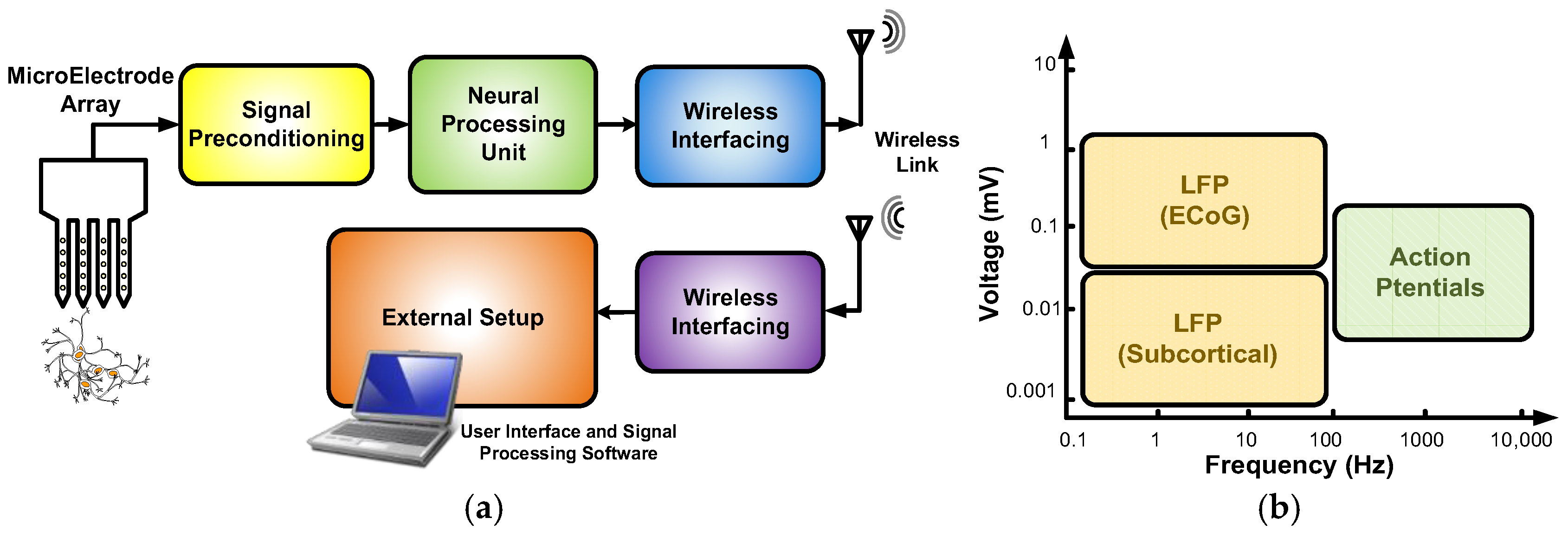
6]. An implantable neural recording microsystem typically consists of recording microelectrode arrays (MEAs), a signal preconditioning module (analog front-end amplifier), a neural processing unit, and a wireless interfacing module (
Figure 1a). The analog front-end amplifier is essential for amplifying weak neural signals and filtering out unwanted frequencies. Extracellular neural signals generally have amplitudes up to 1 mV, concentrated in the 0.1 Hz to 10 kHz range (
Figure 1b) [
7,
8,
9]. These signals include action potentials (APs), indicating the firing of individual neurons, and local field potentials (LFPs), representing grouped neuronal activity. Effective analysis often requires separating LFPs (0.1 Hz to 100 Hz) from APs (100 Hz to below 10 kHz) through preamplification and linear filtering [
7,
8,
9].
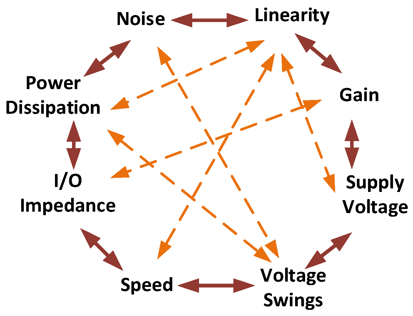
As stated above, the neural signal preconditioning module is essential for amplifying and filtering signals in implantable biomedical microsystems, typically using a preamplifier and a bandpass filter. In some cases, the voltage gain and cut-off frequencies of the signal preconditioning module can be adjusted or programmed. Key attributes of this module include the ability to amplify signals within a specific frequency range, low input-referred noise (IRN) for detecting small spikes, minimal off-chip components to reduce size, and a wide dynamic range for capturing spikes and LFPs ranging from ±(1–2) mV in amplitude at its input terminals. It should also have a high common-mode rejection ratio (CMRR) to reduce power line noise interference and a robust power-supply rejection ratio (PSRR) to handle power supply noise [
9]. Additionally, the input impedance must exceed that of the electrode–tissue interface to avoid signal loss. Consequently, given these existing trade-offs, designing fully integrated neural recording amplifiers and their building blocks, including operational transconductance amplifiers (OTAs), that meet these requirements (low voltage, low power, minimal area, and low IRN) is a significant challenge. In fact, as shown in
Figure 2, it is important to recognize that design parameters frequently involve trade-offs with one another, transforming the design process into a complex, multi-dimensional optimization task. Effectively addressing these challenges demands a blend of intuition and expertise to achieve a balanced and acceptable compromise [
10].
Table 1 summarizes the requirements of neural recording applications and shows the performance requirements for OTAs in these applications [
1,
3].
A variety of circuit techniques and structures have been developed to enhance the performance of OTAs for use in neural recording amplifiers. Each of these approaches aims to improve one or more of the design requirements, such as improving voltage gain and circuit linearity, reducing circuit noise and power consumption, as well as the chip silicon area. Regarding circuit noise reduction, various approaches have been reported. In general, the overall noise of an OTA is a combination of thermal and flicker noise. Flicker noise, often referred to as 1/f noise, is particularly critical for circuits designed for low-noise, low-frequency operation at relatively modest frequencies [
11]. Besides the size of transistors and their operating points, the polarity of transistors also plays a significant role in noise performance. In the realm of neural signal amplifiers, P-channel input MOSFETs are commonly favored over their N-channel counterparts due to their inherent advantages. These include a reduced common-mode (CM) input voltage level, diminished low-frequency noise, and a higher upper −3 dB frequency, particularly when employed in cascode topologies. This combination of attributes results in an extended unity-gain bandwidth, making P-channel MOSFETs an attractive choice for applications demanding high-performance analog front-ends [
12,
13]. It is important to note that this polarity-based noise difference is not universal across all fabrication processes. While input transistors significantly contribute to the IRN, an inadequately designed circuit can lead to the noise from load transistors being amplified by the transconductance ratio. Hence, it is essential for designers to consider the noise of all transistors employed in the circuit design [
14].
To minimize power consumption, circuit noise, and consumed silicon area, various techniques have been employed in previous studies. For example, the CMOS amplifier proposed in [
15] aims to optimize area efficiency for neural recording by utilizing indirect negative feedback, resulting in a low −3 dB cutoff frequency. This allows for minimal capacitance, easily implementable on-chip. Additionally, the circuit proposed in [
15] incorporates attenuators within the feedback loop to further decrease the silicon area required for capacitors while enhancing the circuit’s input impedance. The work presented in [
16] aims to design a high-gain recording read-out circuit with a minimized noise efficiency factor (NEF) by biasing the system in the subthreshold region to lower power consumption, even at high supply voltages. Key contributions include developing a low-power, low-noise neural signal recording circuit; achieving high linearity in signal digitization at a low sampling rate; and creating a graphical user interface for signal processing and analysis. In [
17], source degeneration was applied to a double recycling folded-cascode (RFC) amplifier to lower IRN, although this method also resulted in a reduced output swing and voltage gain. Additionally, studies in [
18,
19,
20] explored the use of chopper amplifiers with positive feedback to meet noise specifications and address the low input impedance characteristic of chopper amplifiers. However, these amplifiers necessitate a clock and supplementary circuits, which can increase both power consumption and overall complexity. In [
21], the implementation of current splitting and scaling techniques in a current mirror OTA has resulted in an improved trade-off between power and IRN. However, this also leads to an increase in chip area and voltage headroom requirements. The open-loop amplifier presented in [
22] boasts a low NEF alongside high CMRR and PSRR. However, open-loop configurations exhibit greater sensitivity to process, voltage, and temperature variations compared to closed-loop designs, resulting in diminished linearity. In [
23], a fully differential amplifier is introduced, which combines an instrumental amplifier with a programmable voltage gain amplifier. However, the inherent asymmetry in the instrumental amplifier structure significantly compromises the amplifier’s linearity.
This work presents a low-noise, low-power amplifier utilizing an RFC architecture for neural recording applications. To enhance performance and reduce chip area, the input stage employs a combination of N-type and P-type MOSFETs compared to conventional all-P-type designs. The incorporation of recycled current and cross-coupled transistors with positive feedback significantly improves voltage gain, DC performance, unity-gain bandwidth, and overall circuit linearity. The remainder of the article is structured as follows.
Section 2 introduces the CMOS RFC OTA, emphasizing its recent advancements.
Section 3 explores the structure and analysis of the proposed fully differential RFC amplifier, providing a thorough comparison with the conventional folded-cascode amplifier.
Section 4 presents the circuit-level post-layout simulation results, including the integration of the designed OTA into a standard neural recording amplifier (NRA) structure. Finally,
Section 5 offers the concluding remarks of the paper.
2. Introduction to CMOS RFC OTA
The OTA is a common component in integrated circuits that are designed to handle large output loads, typically in the form of capacitors rather than resistors. OTAs are frequently used in neural recording circuits. These amplifiers can be implemented through single-stage, two-stage, or multi-stage designs. While multi-stage amplifiers can significantly boost DC gain, their stability in closed-loop configurations can be a major issue. Frequency compensation methods can be employed to establish a dominant pole and ensure stability with a sufficient margin [
24]. However, these techniques unavoidably decrease the unity-gain bandwidth and speed of the OTA. Additionally, the analysis and design of multi-stage amplifiers can be complex. Single-stage OTAs inherently exhibit a dominant real pole, eliminating the need for complex frequency compensation techniques. This inherent stability stems from the presence of a single high-impedance node within the signal path. This characteristic renders single-stage OTAs highly suitable for closed-loop applications. Two prominent architectures for single-stage OTAs are the telescopic-cascode and the folded-cascode topologies. While the telescopic-cascode OTA offers superior performance in terms of speed, DC gain, and reduced IRN and power consumption, the folded-cascode configuration exhibits a distinct advantage in low-voltage scenarios. Its reduced power supply voltage requirement and enhanced output voltage swing make it a more viable option in modern CMOS technologies where supply voltages have dwindled below one volt. In such low-voltage regimes, the output voltage swing of the telescopic-cascode OTA becomes severely limited, rendering it impractical for most applications [
24].
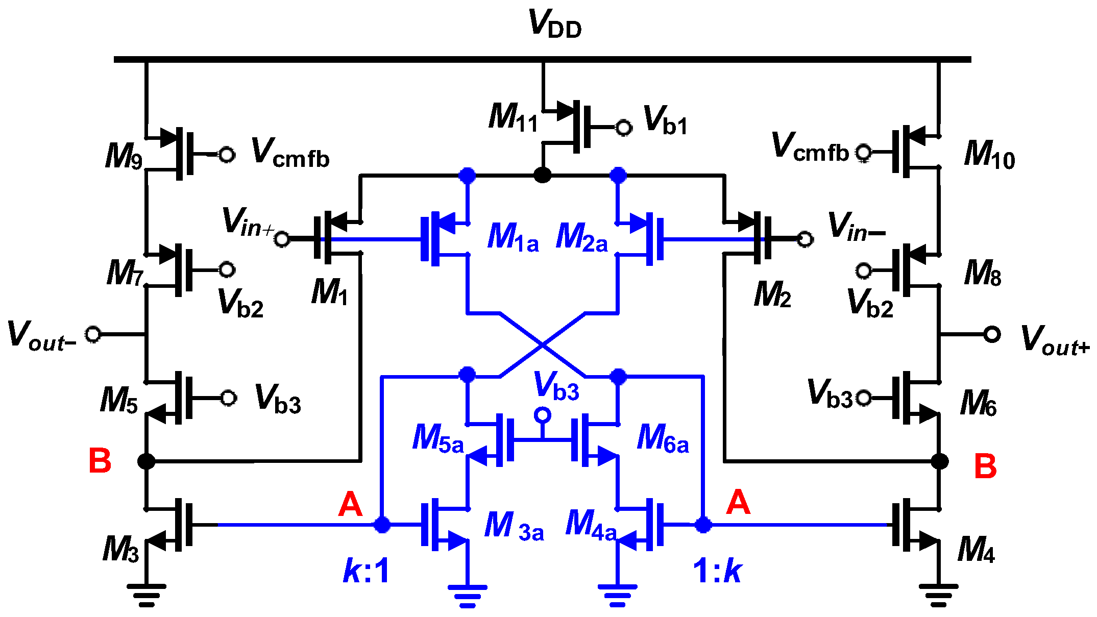
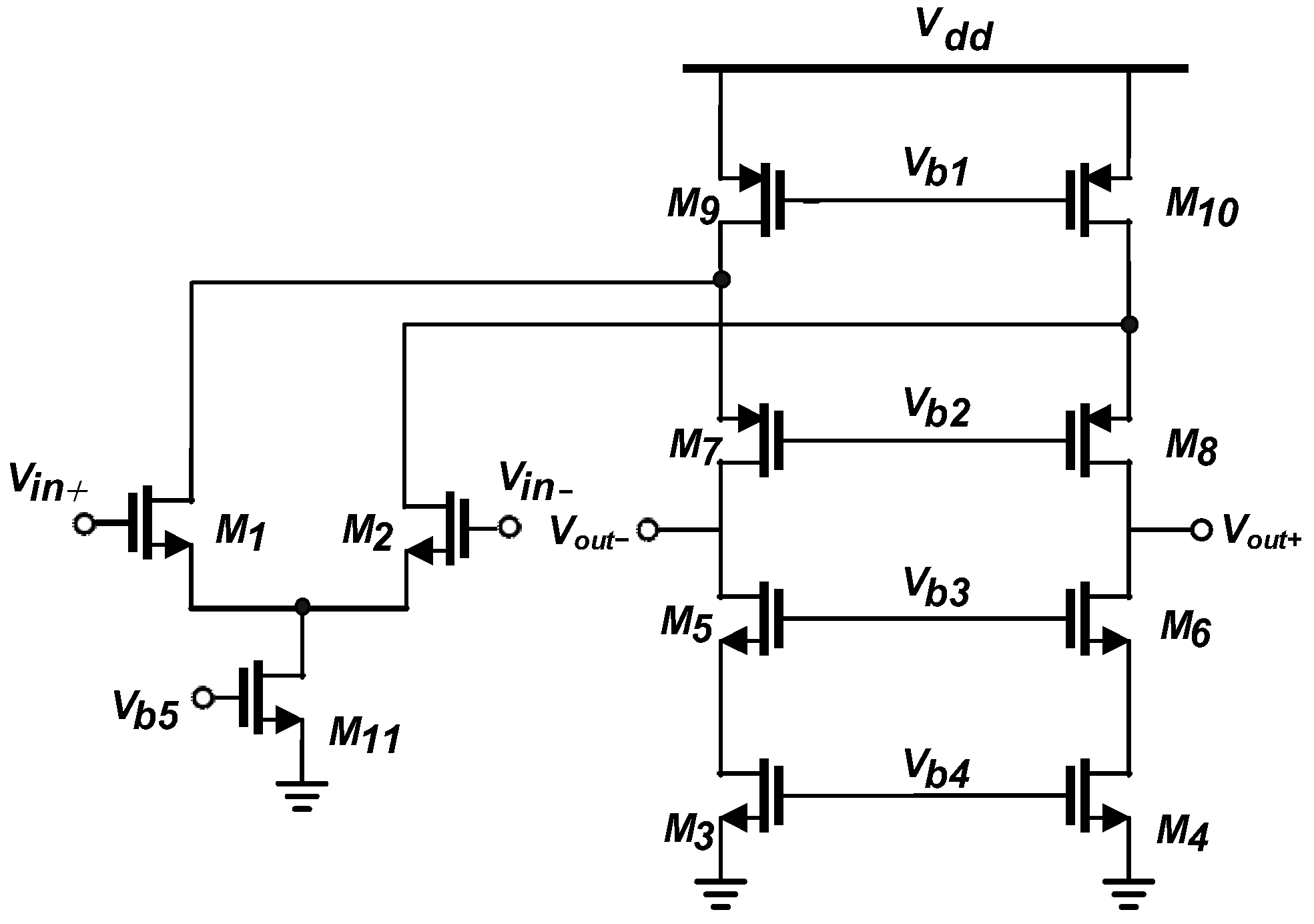
The circuit diagram in
Figure 3 illustrates the structure of a fully differential RFC OTA as described in reference [
24]. In this design, the input devices are divided into
M1,
M2,
M1a, and
M2a to utilize the idle
M3 and
M4 current source transistors from the conventional folded-cascode amplifier in the signal path. Essentially, the RFC amplifier consists of a conventional folded-cascode amplifier and a current-mirror OTA. The conventional folded-cascode amplifier is constructed using M
1–M
11 transistors, while the current-mirror OTA is formed by
M1a,
M2a, and
M3–11 devices. According to [
24] the RFC OTA offers several advantages over the traditional folded-cascode design, such as improved unity-gain frequency and slew rate (SR). Additionally, the DC gain is more than doubled due to lower bias current in the output transistors, which results in higher output resistance. However, this structure may experience a decrease in phase margin due to additional poles. Despite this, the reduction in phase margin may be beneficial for fast-settling applications, where a phase margin of 60 to 70 degrees is ideal, even though the standard folded-cascode OTA typically has a large phase margin of over 80 degrees. In recent years, numerous researchers have focused on enhancing the circuit characteristics of folded-cascode OTA and its more recent variant, the RFC one. The following paragraphs provide a brief overview of several noteworthy circuits that have been developed.
Ref. [
25] introduced a two-path OTA by dividing the input transistors of a conventional telescopic-cascode design, combining elements of both telescopic-cascode and folded-cascode architectures. Building upon this, a fully differential recycling telescopic-cascode OTA is presented in [
26]. This design incorporated an additional current-mirror OTA by splitting the input transistors while also employing current recycling, cross-coupled transistors, and local positive feedback to improve both small-signal and large-signal characteristics. The design in [
27] expands on this concept by splitting the input transistors into three differential pairs to implement a double-RFC OTA. Two of the differential pairs function similarly to an RFC amplifier, while the third pair drives active current mirrors. This innovative arrangement allows for the reuse of shunt bias currents twice, thereby improving OTA performance without incurring additional power or area overhead. The double recycling approach has been further refined in studies referenced in [
28,
29,
30]. A constant-gm rail-to-rail OTA based on an RFC architecture was proposed in [
31]. To improve SR, ref. [
32] introduced additional signal paths in a fully differential RFCA. Subsequently, ref. [
33] employed complementary input pairs for enhanced gain-bandwidth. Asymmetrical current splitting in a single-ended RFCA was investigated in [
34] to boost small-signal transconductance and DC gain. Furthermore, ref. [
35] introduced local positive feedback to a conventional folded-cascode OTA, resulting in improved DC gain, gain-bandwidth, and SR compared to traditional and some advanced recycling designs. Building upon this, ref. [
36] presented a bulk-driven double-RFC OTA for biomedical applications, leveraging positive feedback and self-biased cascode transistors to enhance performance at lower supply voltages.
In reference [
37], a fully differential Class A single-stage OTA is presented for high-speed switched-capacitor applications. The authors aimed to optimize both large- and small-signal performance by incorporating several innovative techniques: current recycling, enhanced phase margin through high-speed current mirrors, and cross-coupled local positive feedback transistors. This multi-pronged approach enabled the realization of fast-settling performance with sufficient accuracy while minimizing power dissipation. A single-stage Class AB OTA, featuring a symmetric design and a significantly enhanced SR, was reported in [
38]. The input stage of this RFC amplifier employs floating gate voltage cells to facilitate Class AB operation. To further augment the SR, the output stage incorporates nonlinear current mirrors and self-biasing techniques. This design achieves an impressive SR, approximately 15 times greater than that of a conventional folded-cascode amplifier, albeit at the cost of slightly increased power dissipation. Furthermore, an adaptive biasing Class AB input stage, utilizing flipped voltage follower (FVF) cells and local common-mode feedback (CMFB) techniques, was implemented to realize a single-ended RFC OTA in [
39]. This approach led to notable improvements in both small-signal transconductance and SR. In [
40], a single-ended class AB amplifier was introduced that achieved optimal performance in terms of SR and small-signal parameters through adaptive biasing and local common-mode feedback techniques. Additionally, dynamic biasing of cascode transistors using quasi-floating gates was utilized to enhance performance. In [
41], various configurations based on this technique were proposed. In [
42], a fully differential class AB RF amplifier with adaptive input biasing and an auxiliary amplifier was introduced to improve DC gain. In [
43], a multi-path fully differential bulk-driven class AB OTA utilizing FVF cells for class AB operation was proposed, resulting in improved small-signal performance and SR in weak inversion. Finally, in [
44], a single-ended bulk-driven class AB OTA combining a double-RFC amplifier with FVF cells and partial positive feedback was suggested.
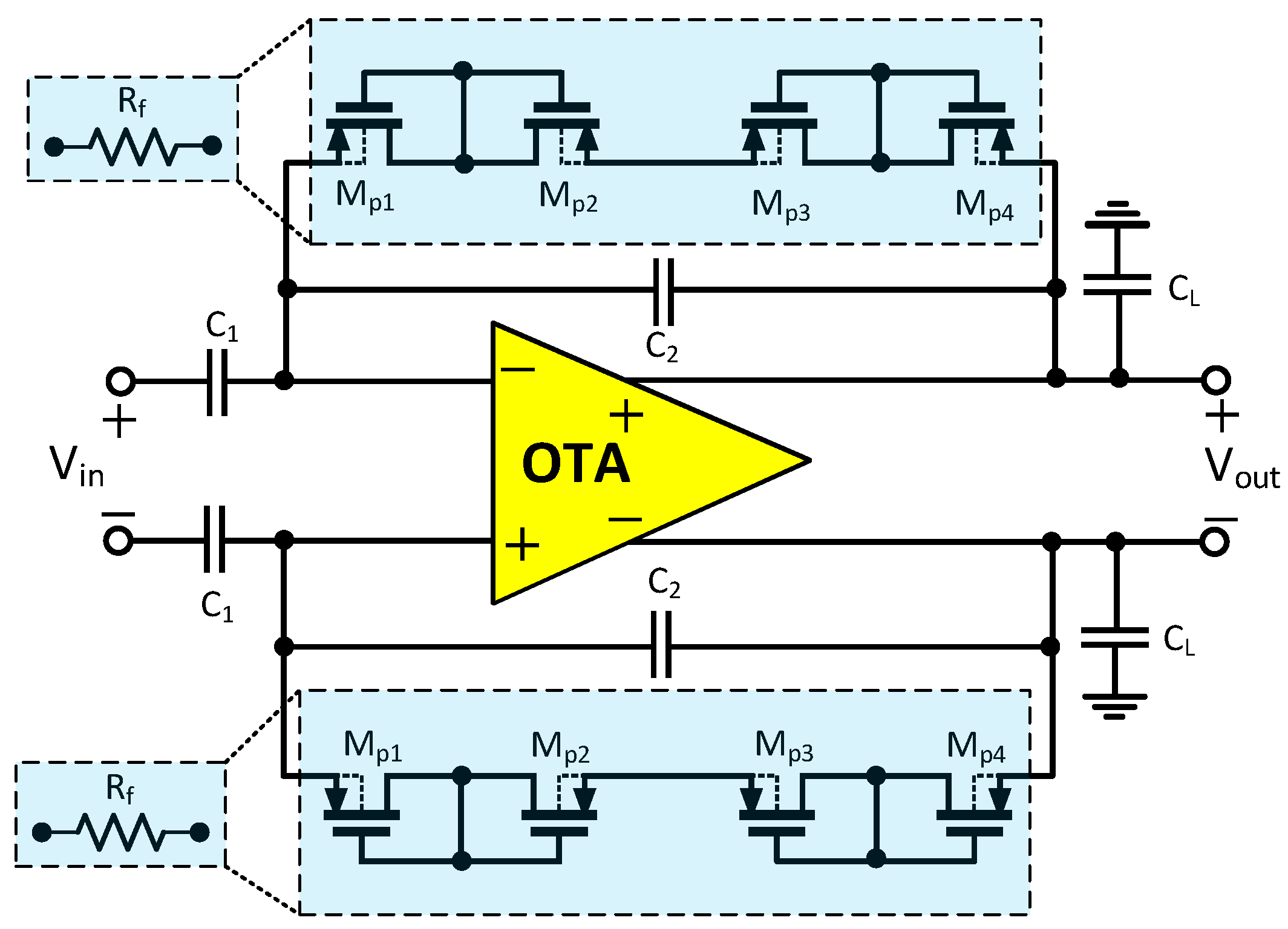
3. Proposed Fully Differential RFC OTA
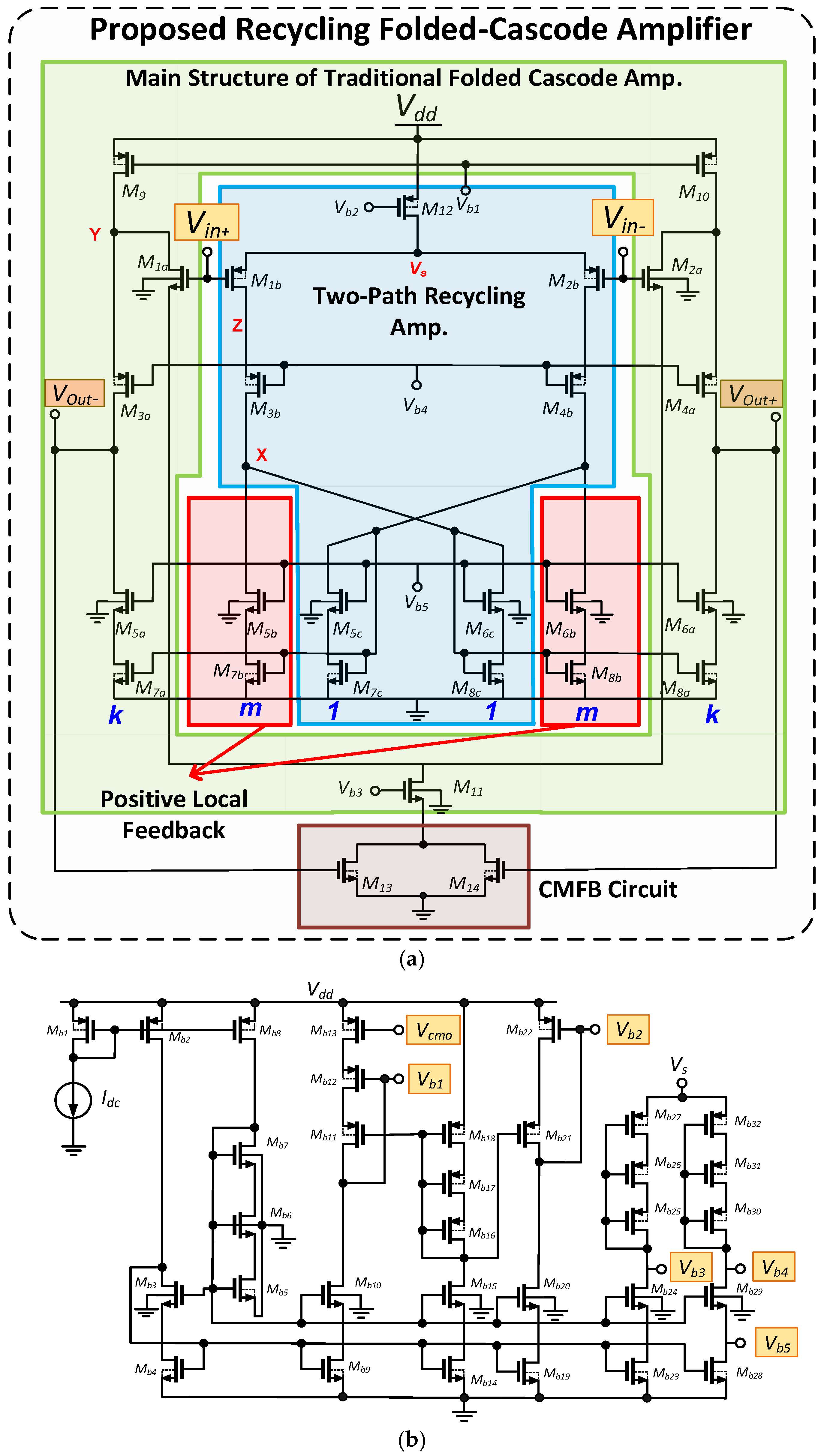
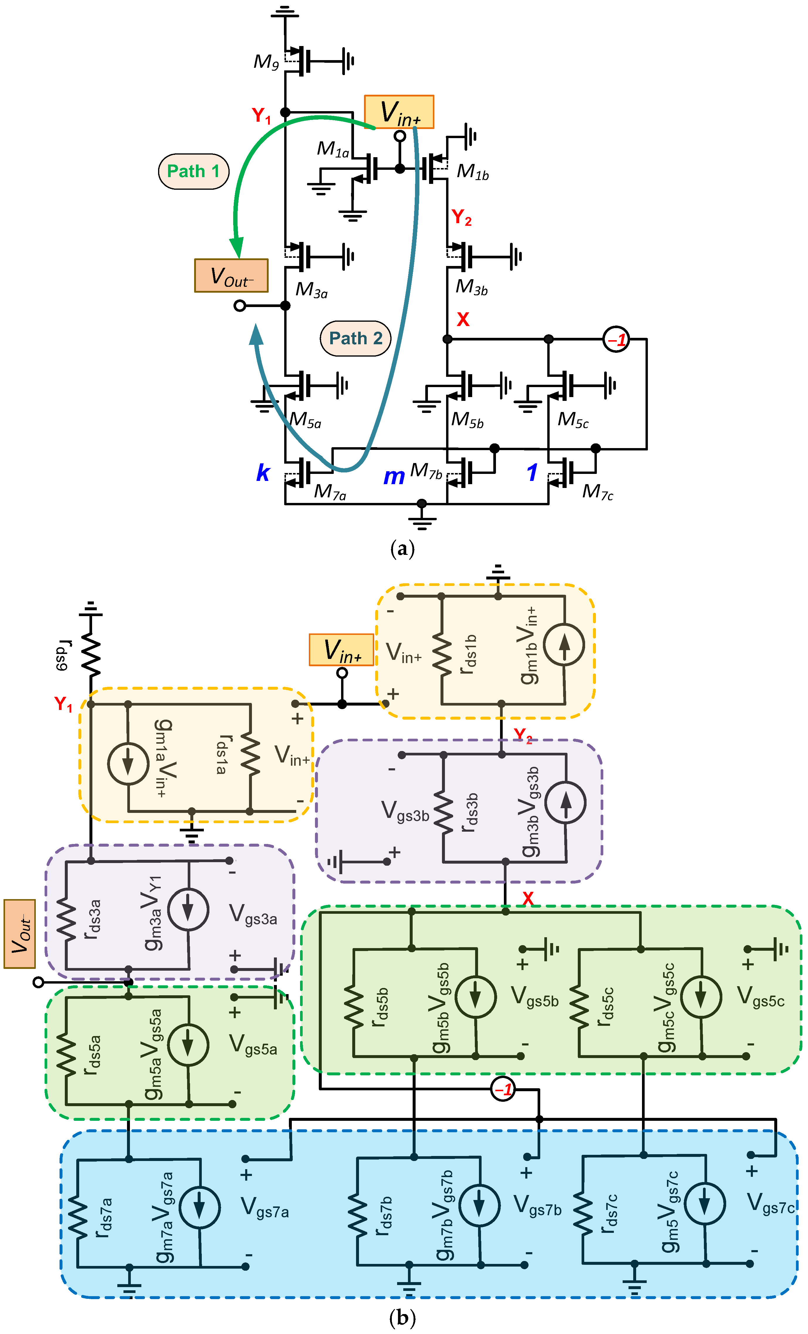
Figure 4a illustrates the presented RFC OTA architecture, which can be considered as a modified version of the amplifier presented in [
26]. The transistors
correspond to their counterparts in a conventional folded-cascode design, which is also shown in
Figure 5. The input stage, comprising
and
devices, is divided for efficient current recycling and reduced output transistor biasing current, thereby enhancing output resistance. All input transistors are oversized to minimize flicker noise and operated in the subthreshold region. Unlike traditional approaches favoring P-type MOSFETs for input transistors, the proposed design incorporates both N-type and P-type devices to expand the input range. While P-type MOSFETs are often preferred for lower flicker noise, this assumption is not universally valid, and a poorly designed circuit can amplify noise from load transistors. Hence, the noise contribution of all important transistors should be carefully considered. To create a two-path amplifier, transistors
and
are paired. Transistors
and
form a cascode current mirror for improved matching, while
,
,
and
devices implement a cross-coupled configuration instead of a current mirror to introduce local positive feedback at the gates of
and
devices [
45]. The aspect ratio of
family transistors compared to each other, and similarly the aspect ratio of
family transistors to each other, are shown by the coefficients k and m in
Figure 4a. Further explanations regarding these coefficients and their relationship to each other will be provided in the following paragraphs.
As mentioned above, to minimize power consumption and IRN, the input devices were biased in the subthreshold region by maximizing their transconductance and dimensions. This approach concurrently reduced transistor mismatch, enhancing common-mode parameters like CMRR and PSRR while lowering input-referred offset voltage. The biasing voltages
through
are supplied by a constant current biasing circuit with an ideal current source, which is shown in
Figure 4b. Wide-swing cascode current mirrors are used to improve the matching between biasing and main transistors without the swing reduction at the output node of the designed amplifier [
26].
In the presented circuit, the bias values and dimensions of the devices used in the conventional folded-cascode amplifier are selected in such a way that the following equation holds for the currents of transistors
M1a,
M7a,
M2a, and
M8a:
The parameters
k and
m can be selected independently. However, if the relationship
k = m + 1, as suggested in reference [
26], is satisfied, then for the currents flowing through the transistors used in the proposed symmetric circuit, as well as their corresponding transconductance, the following relationships hold:
Given the choice of
k = m + 1 in the proposed circuit, it can be easily proven that
To set the output voltage of the presented amplifier to the desired value (
Vcmo), a CMFB circuit introduced in [
26] is utilized. In this design,
is set to
Vdd/2 as the intended output CM voltage by the biasing circuit. As detailed in [
26], a single tail current source at the input transistors’ sources cannot effectively define the common-mode voltage at the output nodes. This is due to the near-zero voltage gain of the CMFB loop resulting from two opposing CMFB paths. To address this effect, separate tail current sources for the input transistors are employed in this work. These sources, in conjunction with the negative CMFB loop implemented by the main amplifier, establish the CM voltage at the output nodes. Specifically, transistors
and
, identical devices, are utilized at the source of the
tail current source to form the CMFB circuit.
and
operate in the deep triode region, creating a resistance at the source of
, as follows:
In this context, represents the mobility of electrons, signifies the oxide capacitance per unit area, and and denote the aspect ratio and threshold voltage of transistors and , respectively. The operation of the CMFB circuit can be described as follows: A decrease in the common-mode voltage at the output nodes leads to a corresponding increase in the equivalent on-resistance of transistors and , resulting in a larger voltage drop across these devices. Consequently, the bias current of the tail current source decreases. Conversely, the bias current of transistors through is determined by the tail current source and the aspect ratio of the current mirror transistors, which remains relatively constant during common-mode operation. As a result, the drain current of and becomes higher than that of and devices. To satisfy Kirchhoff’s current law at the output nodes, the CM voltage of the output nodes must increase due to the channel length modulation effect of MOSFETs. This necessitates a negative CMFB loop to regulate the output CM voltages. A similar but opposite scenario occurs when the output CM voltage goes above . It should be noted that during differential signal amplification of the designed circuit, Rn remains constant, and the CM voltage at the output nodes does not change significantly.
To calculate the DC voltage gain of the presented circuit,
Figure 6, which shows the half-circuit differential model of the circuit in AC mode, as well as the small-signal model of the presented circuit in the half-circuit differential model, is drawn. As shown in
Figure 6a, four nodes of X, Y
1, and Y
2 and the output voltage in the signal paths have contribution on signal amplification. As indicated in
Figure 6a, the signal path from input to output is established through two different routes, denoted by paths 1 and 2. In general, for multi-path amplifiers, such as the two-path configuration presented in this paper, if the voltage gain signs of both paths are identical, the overall voltage gain is indeed the sum of the individual path gains [
10]. It is important to note that each signal path may have variations in the number of transistors and other utilized elements, which can introduce zeros in the overall transfer function. By utilizing the small-signal model of
Figure 6b (along with acceptable approximations such as ignoring the transistor’s body effect) and based on the superposition theorem, the voltage gain of the circuit can be obtained as follows:
where
is the voltage gain of path 1. In the calculation of
, transistor
M1a acts as the primary amplifying element, and the voltage gain is calculated based on the principles of a common-source amplifier as follows:
in Equation (5) is the path 2 voltage gain. In the calculation of
, a transistor combination involving
M1b and
M3b devices acting as a cascode structure is encountered. The voltage gain of this section is approximated as the transconductance of transistor
M1b multiplied by the resistance seen from node X. Furthermore, due to the signal path extending from node X to the output node, transistor
M7a, in common-source configuration, causes the voltage gain of path 2 to be calculated as follows:
Moreover,
where
,
,
and
represent the equivalent capacitances at the output,
X,
and
nodes, respectively. Based on KCL and KVL, the magnitude of
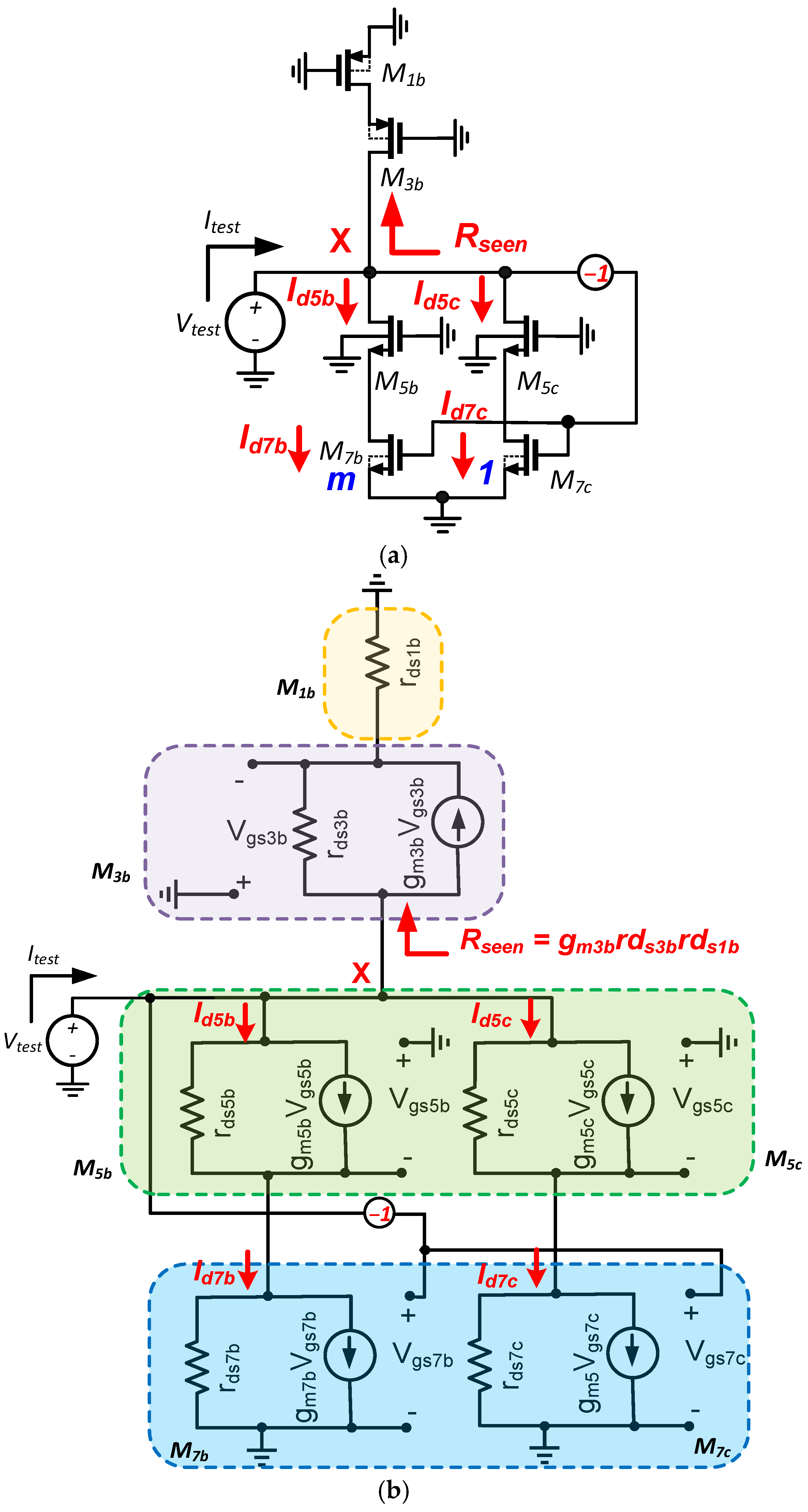
RX, which represents the resistance seen from node X in
Figure 6b, is determined by dividing
Vtest by
Itest in
Figure 7 as follows:
As depicted in
Figure 7, the current
Itest flows through transistors
M5b,
M5c, and
M3b. It is important to note that the contribution of transistor
M3b in this current division is represented by the resistance
Rseen. However, since
Rseen is significantly larger than the resistances resulting from the currents
Id5b and
Id5c, its effect can be safely neglected. Consequently, the current
Itest can be calculated as follows, based on
Figure 7:
It is evident that the currents in the series transistors, specifically the pairs
M5b and
M7b, and
M5c and
M7c, are equal. Consequently,
where
By neglecting the channel length modulation effect and considering that V
gs7b and V
gs7c are equal to
Vtest in magnitude, the resistance
Rx can be easily calculated as follows:
The output resistance of the proposed amplifier can also be calculated by performing some KVLs and KCLs, as described in reference [
10], using
Figure 6b, as follows:
Consequently, by combing Equations (13) and (14), A
2 is calculated as follows:
It should be noted that although there is a difference between the time constant of
and
nodes, but if it is assumed that the poles of these nodes are approximately equal, the transfer function of the designed circuit is simplified to the following:
where
It should be noted that in the context of the proposed amplifier,
gm signifies the small-signal transconductance of the transistors, while r
ds denotes their small-signal drain-source resistance. Assuming a dominant pole at the output node, the unity-gain bandwidth can also be calculated using the following formula:
In the noise analysis, the input transistors and the current mirror devices contribute the most to the noise analysis, and the effects of other devices can be neglected. The IRN is generally composed of thermal noise and flicker noise. The power spectral density of the input-referred thermal noise can be calculated using Equation (19), and the power spectral density of the input-referred flicker noise can be calculated using Equation (20) by performing some mathematical operations. Consequently, the total power spectral density of the IRN can be obtained by combining the above-mentioned equations.
where
Kn and
Kp are the process-dependent flicker noise parameters for N-channel and P-channel devices, respectively;
Cox is the gate oxide capacitor per unit area;
T is the absolute temperature;
k is the Boltzmann constant; and γ is the excess noise factor. It should be noted that there are some trade-offs between noise, stability, and voltage gain in choosing m and k values. The pole associated with node X is typically smaller than the other non-dominant poles, as the transconductance of
M7b and
M7c is smaller than the transconductance of
M3a and
M3b devices (Equation (2)). Therefore, to achieve a sufficient phase margin and ensure stable behavior, the values of
m and
k must be carefully chosen. Increasing
m, and consequently
k, enhances the DC gain and IRN. However, this also reduces the equivalent second pole, which is primarily determined by
RX. This trade-off can be managed by judiciously selecting the aspect ratio of the cross-coupled transistors. In this paper, to simultaneously satisfy the amplifier’s stability, voltage gain, and noise requirements, we have selected
and
as suggested in [
26].


