Abstract
This paper presents a multiple-input single-output (MISO) shadow filter implemented using multiple-input differential difference transconductance amplifiers (MI-DDTAs). The MI-DDTA’s multiple inputs are realized through the multiple-input bulk-driven MOS transistor (MI-BD MOST) technique. Leveraging the multiple-input capability of the DDTA, various filter responses—low-pass filter (LPF), high-pass filter (HPF), band-pass filter (BPF), band-stop filter (BSF), and all-pass filter (APF)—can be efficiently achieved by appropriately configuring the input signals. The natural frequency and quality factor of the shadow filter can be independently tuned using external amplifiers. Unlike conventional shadow filters, where adjusting the quality factor or natural frequency impacts the passband gain, this design ensures a constant unity passband gain. The MI-DDTA operates at a supply voltage of 0.5 V and consumes 385.8 nW of power for setting current Iset = 14 nA. The proposed MI-DDTA and shadow filter are designed and validated through simulations in the Cadence design environment, using a 0.18 µm CMOS process provided by TSMC (Taiwan Semiconductor Manufacturing Company Limited).
1. Introduction
Usually, adjusting the natural frequency and quality factor of second-order filters, such as low-pass filters (LPF), high-pass filters (HPF), band-pass filters (BPF), band-stop filters (BSF), and all-pass filters (APF), can be achieved by tuning the values of internal components, such as resistances, capacitances, and transconductances. Unfortunately, adjusting these internal components affects the performance of the second-order filters. Therefore, shadow filters, also known as agile filters, have been proposed [1,2,3]. This type of filter is composed of a second-order filter and external amplifiers, and the amplifiers are used to control the natural frequency and quality factor, without affecting the perfect performance of the original second-order filters.
There are many shadow filters, also known as agile filters, available in the open literature, based on different active components:
- Transconductance Amplifier (TA) [4,5];
- Current Conveyor (CC) [6,7,8];
- Current-Feedback Operational Amplifier (CFOA) [9,10];
- Operational Transresistance Amplifier (OTRA) [11];
- Current Difference Transconductance Amplifier (CDTA) [12,13,14,15];
- Operational Floating Current Conveyor (OFCC) [16];
- Voltage Differencing Transconductance Amplifier (VDTA) [17,18,19,20];
- Current Backwards Transconductance Amplifier (CBTA) [21];
- Voltage Differencing Differential Difference Amplifier (VDDDA) [22];
- Voltage Differencing Gain Amplifier (VDGA) [23];
- Current Controlled Current Differencing Cascaded Transconductance Amplifier (CC-CDCTA) [24];
- Current Conveyor Cascaded Transconductance Amplifier (CCCTA) [25,26];
- Differential Current Conveyor Cascaded Transconductance Amplifier (DCCCTA) [27].
However, these shadow filters require a relatively high supply voltage and consume significant power because the active devices used in them are not designed for low-voltage and low-power operation. Moreover, when tuning the quality factor and natural frequency using amplifiers, the passband gains of these filters vary, either increasing or decreasing. As a result, additional amplifiers are required to adjust the passband gain to unity [22]. Recently, shadow filters designed to operate with low supply voltage and low power consumption have been proposed [28,29]. However, the passband gains of these filters vary when the quality factor and natural frequency are adjusted using amplifiers.
This paper presents a low-voltage, low-power shadow filter utilizing multiple-input differential difference transconductance amplifiers (DDTAs). The multiple inputs of the DDTA are implemented using the multiple-input bulk-driven MOS transistor (MIBD-MOST) technique, while transistors operating in the subthreshold region ensure low-power consumption. The multiple inputs of the DDTA can be utilized to realize a multiple-input single-output shadow filter. Various filtering functions, such as LPF, HPF, BPF, BSF, and APF, can be obtained by appropriately applying the input signals. The natural frequency and quality factor of the filter can be controlled using amplifiers. Unlike previous shadow filters, the passband gain of the proposed filter does not change when the natural frequency and quality factor are varied by the amplifiers. To the best of the authors’ knowledge, no shadow filter operating in this manner has been reported in the literature. The low voltage supply and ultra-low power consumption make the DDTA ideal for applications with limited bandwidth, such as those in biomedical systems, where the signal frequencies range from subhertz to 10 kHz. The proposed MI-DDTA and shadow filter are designed and validated through simulations in the Cadence design environment, using a 0.18 µm CMOS process.
2. Circuit Description
2.1. Multiple-Input Multiple-Output DDTA
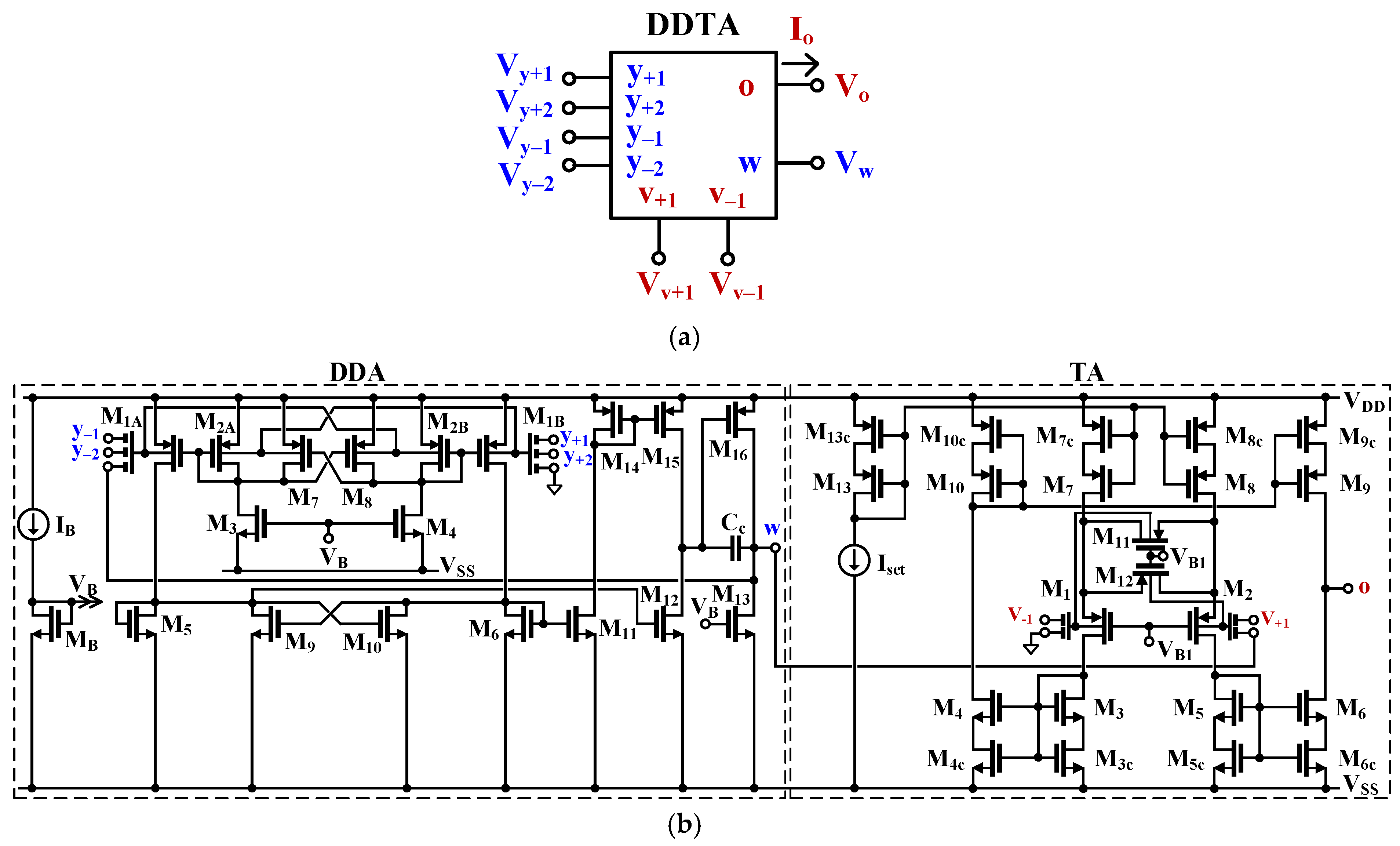
The symbol and CMOS structure of the multiple-input multiple-output differential difference transconductance amplifier (DDTA) are shown in Figure 1. This design features a multiple-input differential difference amplifier (DDA) followed by a multiple-input transconductance amplifier (TA), which was initially introduced in [28,30]. The multiple-input capability of the DDTA is achieved through the multiple-input bulk-driven MOS transistor technique, which eliminates the need for additional MOS differential pairs, thereby reducing power consumption. The symbol and implementation of the multiple-input MOST are depicted in Figure 2. The multiple-input functionality is achieved by connecting capacitors CB in parallel, along with a high-resistance anti-parallel connection of two minimum-size transistors ML. The capacitors are realized using metal–insulator–metal (MIM) technology, which is readily available in modern CMOS processes.

Figure 1.
Proposed DDTA, (a) electrical symbol, (b) CMOS implementation.
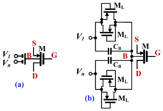
Figure 2.
The BD MI-MOST: symbol (a) and implementation (b).
To meet the specific requirements of our filter application, the number of DDA inputs is increased compared to those in [28,30]. Although this modification results in a slight increase in the DDTA chip area, it does not impact its power consumption, which remains a key advantage of the proposed technique. Furthermore, the adoption of multiple-input MOST simplifies the implementation of filter applications by reducing the number of active elements required, thereby potentially decreasing both the overall chip area and power consumption compared to traditional designs.
The experimental validation of the standalone multiple-input TA was presented in [31]. To enable the circuit to operate at supply voltages close to the threshold voltage of a single MOS transistor, the design functions in the subthreshold region. The differential pairs in the DDA and TA utilize bulk-driven transistors with multiple-input capability, allowing the input voltage swing to extend up to rail-to-rail. However, as the bulk-driven and multiple-input techniques inherently reduce the voltage gain of the circuit, partial positive feedback and a self-cascode structure have been employed to mitigate this drawback, as detailed in [31].
The function of the DDTA can be expressed as follows:
The input stage (DDA) performs the addition and subtraction of voltage signals with a multiple-input unity gain configuration, as represented by . The output stage (TA) uses a multiple-input transconductance gain, defined as . The multiple-input capability of this device allows for the easy implementation of various filter responses. Additionally, when the input terminals of the DDTA are at a high-impedance level, they can be directly connected to any source without requiring additional buffer circuits.
2.2. Proposed Shadow Filter
The original multiple-input single-output shadow filter is shown in Figure 3a [3]. This filter utilizes external amplifiers , , and to adjust the quality factor and natural frequency. However, adjusting these parameters also affects the passband gain of the transfer functions for LPF, HPF, BPF, BSF, and APF, as discussed in [6,8,28,29]. Figure 3b illustrates a technique designed to maintain a constant passband gain when the quality factor and natural frequency are adjusted by the amplifiers. Compared to Figure 3a, the block diagram in Figure 3b introduces the input (i.e., ) to preserve constant passband gain. The input is applied alongside the input signal under appropriate conditions.
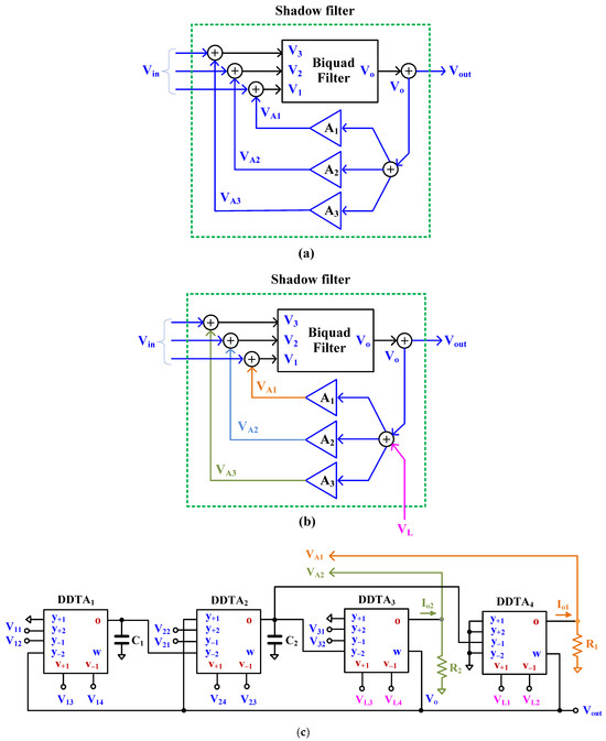
Figure 3.
Proposed shadow filter, (a) conventional block diagram, (b) improved block diagram, and (c) proposed shadow filter using MI-DDTAs.
In comparison to Figure 3b, the components DDTA1, DDTA2, C1, and C2 form a biquad filter, while DDTA4 and R1 create amplifier , and DDTA3 and R2 form amplifier . These two amplifiers, and , are sufficient for the independent control of the natural frequency and quality factor.
The input voltages , , , and are applied to the input signals and/or the voltages and , depending on the required filtering functions. By neglecting the feedback connections of and , and using (1) along with nodal analysis, the output voltage can be expressed as follows:
The non-inverting LPF can be achieved by applying the signal to the input or . The non-inverting BPF can be achieved by applying the signal to the input or , and the non-inverting HPF can be achieved by applying the signal to the input . The inverting LPF can be obtained by applying the input signal to the input or , the inverting BPF can be obtained by applying the input signal to the input or , and the inverting HPF can be obtained by applying the input signal to the input . It should be noted that both non-inverting and inverting BSF and APF can be also realized.
Considering the DDTA4, R1 () and the DDTA3, R2 (), using (1) along with nodal analysis, the voltage gains of the amplifiers and can be expressed by the following:
The voltage gain can be controlled by and/or , while the voltage gain can be controlled by and/or . From Equations (3) and (4), the voltages and can be expressed, respectively, as and .
- Case 1
The output voltage of the amplifier () is used as the input for , while the output voltage of the amplifier () is used as the input for . By applying suitable input signals, various filtering functions can be obtained as follows:
- BPF
The input signal is applied to the input , while the inputs , , , and are grounded, the input is connected to (). Input is connected to (). With these conditions, Equation (2) becomes the following:
The final transfer function of non-inverting BPF can be expressed as follows:
If the input signal is applied to the input , while input is grounded, and other conditions remain unchanged, then the transfer function of inverting BPF can be obtained as follows:
- HPF
The input signal is applied to the input along with input (), while the inputs , , , , and are grounded. Input is connected to (), and input is connected to (). With these conditions, Equation (2) becomes the following:
The final transfer function of non-inverting HPF can be expressed as follows:
- LPF
The input signal is applied to the input along with input (), while the inputs , , and , , are grounded. Input is connected to (), and input is connected to (). With these conditions, Equation (2) becomes the following:
The final transfer function of LPF can be expressed as follows:
If the input signal is applied to the input , while input is grounded, and other conditions remain unchanged, the transfer function of inverting LPF can be obtained as follows:
- BSF
The input signal is applied to the inputs and along with inputs and (), while the inputs , , , and are grounded. Input is connected to (), and input is connected to (). With these conditions, Equation (2) becomes the following:
The final transfer function of non-inverting BSF can be expressed as follows:
- APF
The input signal is applied to the inputs , , and along with inputs and (), while the inputs , , , , , and are grounded. Input is connected to (), and input is connected to (). With these conditions, Equation (2) becomes the following:
The final transfer function of APF can be expressed as follows:
Letting , (), the parameters and of the filters in case I can be expressed by the following:
The quality factor can be controlled by the factor . Importantly, adjusting the quality factor does not affect the passband gain of any of the filtering functions. This is achieved by adding the input signal to the amplifier inputs (i.e., ) to compensate for the voltage gain when the quality factor is varied by the factor
It is worth noting that the shadow filter in Case 1 provides non-inverting transfer functions for LPF, HPF, BPF, BSP, and APF and inverting transfer functions for LPF and BPF.
- Case 2
In case 1, the output voltage of the amplifier () is used as the input , and the output voltage of the amplifier () is used as the input for . The amplifiers and are set to be equal () and are used to control the quality factor. In case 2, the amplifier is used to control the natural frequency, while the amplifier is used to control the quality factor. In this case, the output voltage of amplifier () is used as the input , and the output voltage of amplifier () is used as the input for .
- HPF
The input signal is applied to the input , while the inputs , , , and are grounded; the input is connected to (). Input is connected to (). With these conditions, Equation (2) becomes the following:
The final transfer function of non-inverting HPF can be expressed as follows:
If the input signal is applied to the input , while input is grounded, and other conditions remain unchanged, the transfer function of inverting HPF can be obtained as follows:
- LPF
The input signal is applied to the input along with input (), while the inputs , , , , and , , are grounded. Input is connected to (, and input is connected to (). With these conditions, Equation (2) becomes the following:
The final transfer function of LPF can be expressed as follows:
If the input signal is applied to the input , while input is grounded, and other conditions remain unchanged, then the transfer function of inverting HPF can be obtained as follows:
- BPF
The input signal is applied to the input along with input (), while the inputs , , , and , , are grounded. Input is connected to (), and input is connected to (). With these conditions, Equation (2) becomes the following:
The final transfer function of non-inverting BPF can be expressed as follows:
If the input signal is applied to the input , while input is grounded, and other conditions remain unchanged, then the transfer function of inverting BPF can be obtained as follows:
- BSF
The input signal is applied to inputs and along with inputs (), while the inputs , , , , , and are grounded. Input is connected to (), and input is connected to (). With these conditions, Equation (2) becomes the following:
The final transfer function of non-inverting BSF can be expressed as follows:
If the input signal is applied to inputs and , while inputs and are grounded, and other conditions remain unchanged, then the transfer function of inverting BSF can be obtained as follows:
- APF
The input signal is applied to inputs , , and along with inputs , and (), while the inputs , , , , , , and are grounded. Input is connected to (), and input is connected to (). With these conditions, Equation (2) becomes the following:
The final transfer function of APF can be expressed as follows:
If the input signal is applied to inputs , , and , while inputs , , and are grounded, and other conditions remain unchanged, then the transfer function of inverting APF can be obtained as follows:
It is worth noting that the shadow filter in Case 2 provides both non-inverting and inverting transfer functions for LPF, HPF, BPF, BSP, and APF.
The parameters and can be given by the following:
The parameter can be controlled by the factor . However, due to the variation parameter , the factor is required to adjust and maintain a constant . Unlike previous shadow filters, where adjusting the parameter affects the passband gain [6,8,28,29], the passband gain of the proposed shadow filter remains constant.
2.3. Non-Ideal Analysis
Considering the non-idealities of DDTA, (1) can be rewritten as follows:
Here , where represents the voltage tracking error from the -terminal to the -terminal. Similarly, , where denotes the voltage tracking error from the -terminal to the -terminal of the k-th DDTA and the-th input terminal. The parameter represents the non-ideal transconductance gain of the DDTA. In the frequency range near the cut-off frequency, can be approximated as follows:
where , denotes the first-order pole.
Using (36), the denominator of transfer function in case 1 can be expressed as follows:
Substituting and from Equation (37) into Equation (38), it becomes the following:
The non-ideal effect of the transconductance of the OTA can be neglected by satisfying the following conditions:
The parameters and in (17), (18) can be rewritten as follows:
Here, , .
Using (36), the denominator of transfer function in case 2 can be expressed as follows:
Substituting and from Equation (37) into Equation (43), it becomes the following:
The non-ideal effect of the transconductance of the OTA can be neglected by satisfying the following conditions:
The parameters and in (34), (35) can be rewritten as follows:
This can be achieved by appropriately selecting the values of transconductances , , and capacitances and to create large time constants, which are significantly greater than the small-time constants associated with non-ideal effects.
3. Results
The circuit was developed in the Cadence environment using the 0.18 µm TSMC CMOS technology. A supply voltage of 0.5 V was applied (±0.25 V for simulation), with a bias current of 40 nA for the MI-DDA and a tunable setting current for the TA. The aspect ratios of the transistors, capacitor values, and bias voltages are provided in Table 1. The power consumption for the MI-DDTA with Iset = 14 nA was 385.8 nW. Detailed simulation results of the MI-DDTA can be found in [28,30].

Table 1.
Transistor aspect ratio of the MI-DDTA.
The simulation results for the filter design in case I were selected for presentation. The component values were set as follows: C1 = C2 = 25 pF, R1 = R2 = 4 MΩ, Iset = Iset1 − Iset4 = 14 nA. The magnitude and phase responses of the filter for various configurations—(a) LPF, (b) HPF, (c) BPF, (d) BSF, and (e) APF—are illustrated in Figure 4. The filter’s cutoff frequency was 251.18 Hz with a total power consumption of 1.543 μW.
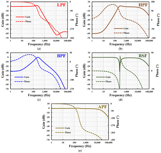
Figure 4.
Filter magnitude and phase responses with setting current Iset = 14 nA for: (a) LPF, (b) HPF, (c) BPF, (d) BSF, and (e) APF.
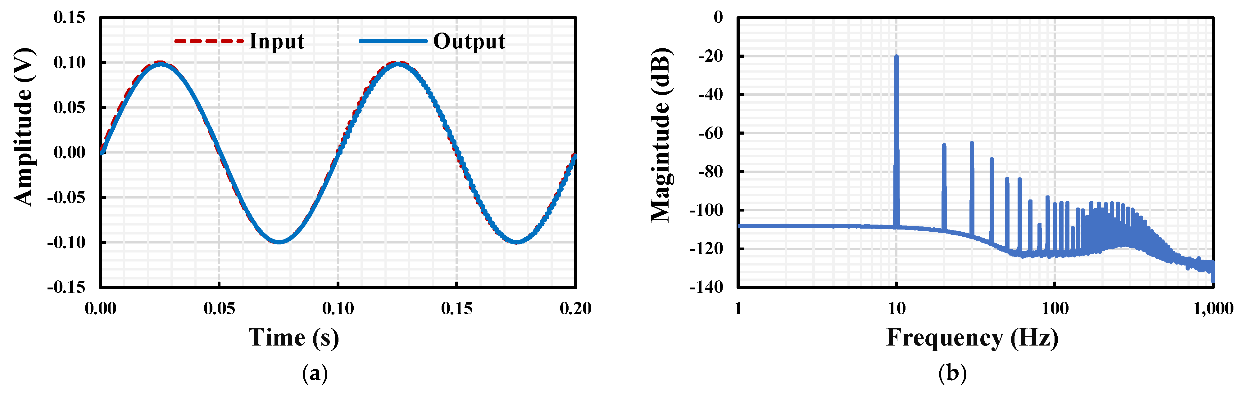
Figure 5 illustrates the performance of the LPF through the following: (a) displays the transient response when a sine wave with an amplitude of 0.1 V and a frequency of 10 Hz is applied to the input, while (b) presents the output signal spectrum, showing a total harmonic distortion (THD) of 0.8%.

Figure 5.
Transient response of the LPF (a) and the spectrum of the output signal (b).
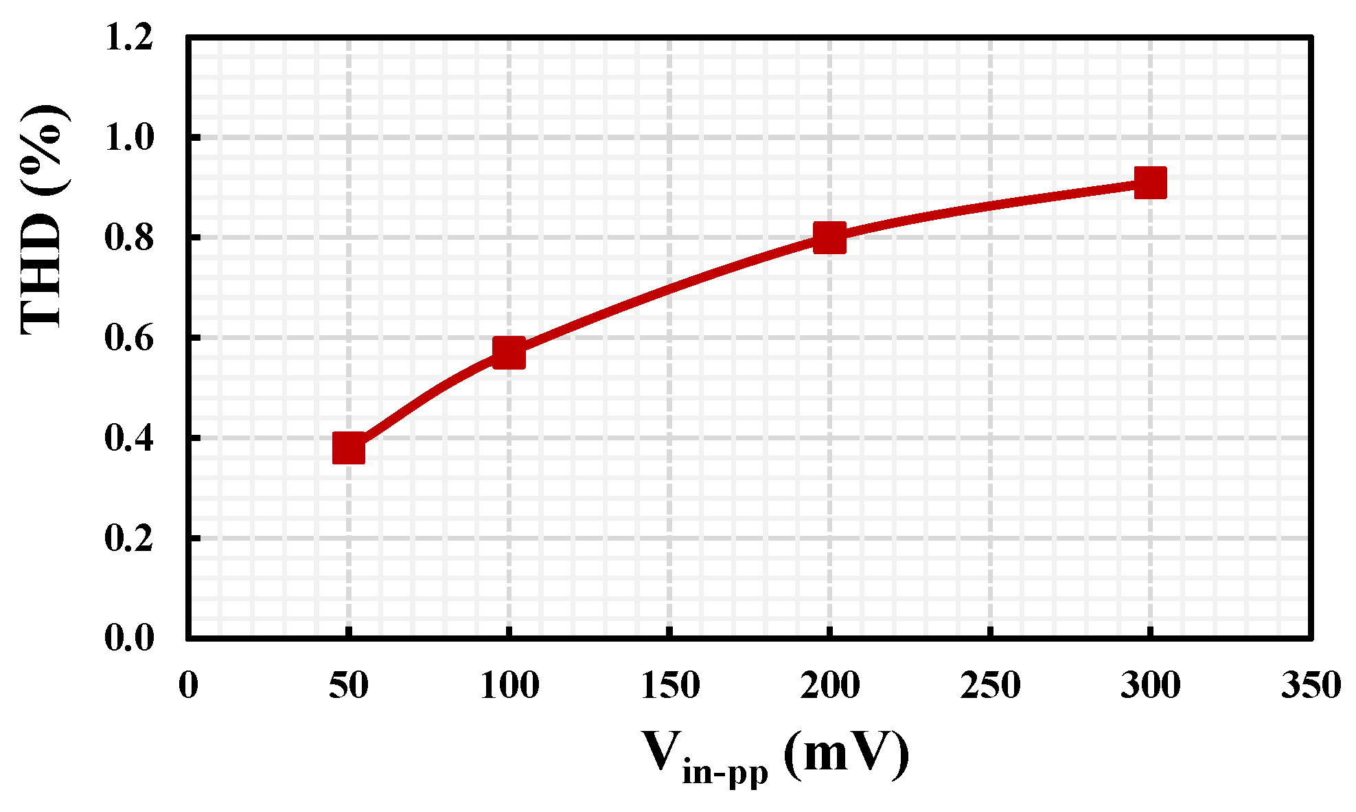
The THD for the LPF was measured by applying a sine wave signal with a frequency of 10 Hz and varying amplitudes at the input. As shown in Figure 6, the filter demonstrates a THD of less than 1% for a 300 mV peak-to-peak signal.

Figure 6.
THD of the LPF.
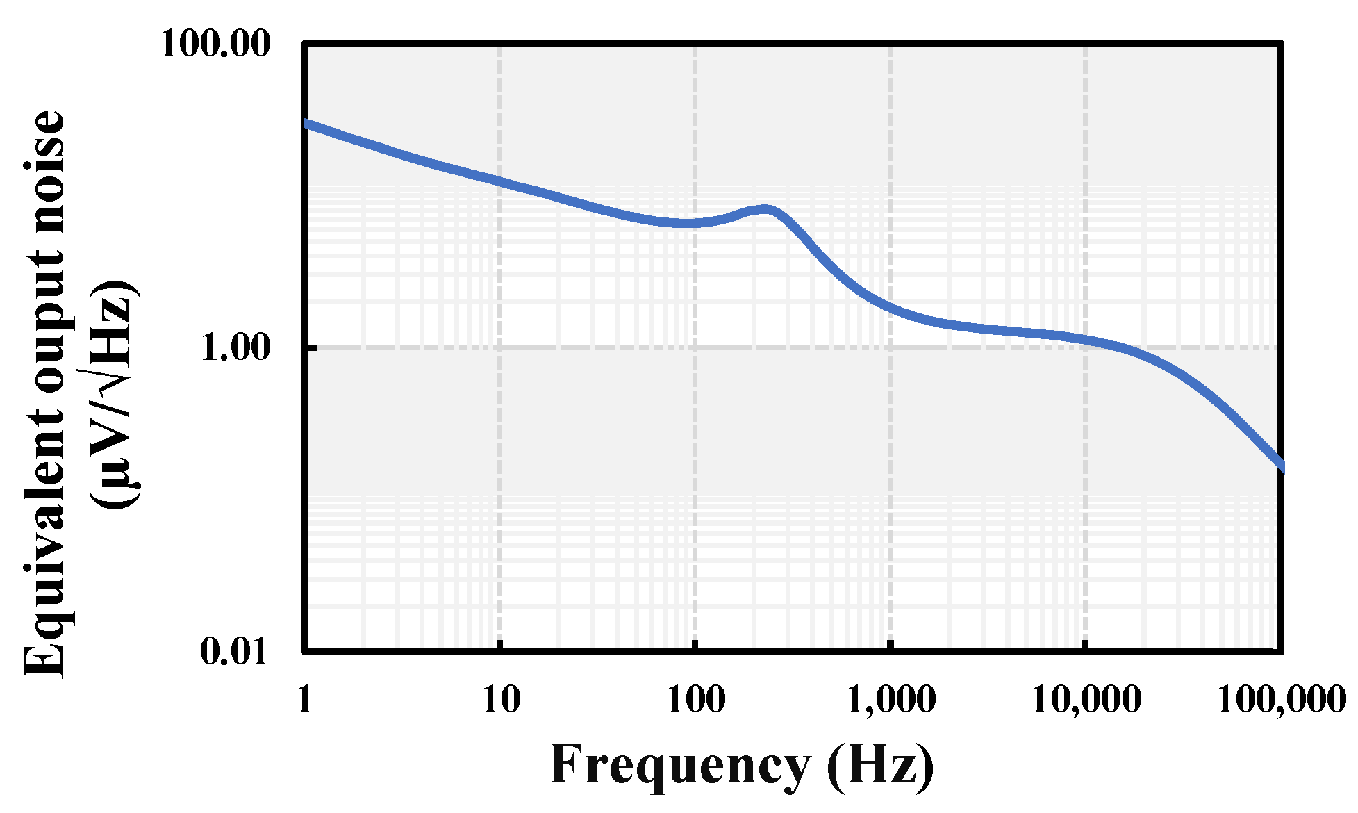
Figure 7 illustrates the equivalent output noise of the LPF. The output integrated noise within the LPF’s bandwidth was calculated to be 128.9 µV. Consequently, the dynamic range is 58.3 dB for a 1% total harmonic distortion (THD).

Figure 7.
Output noise of the LPF.
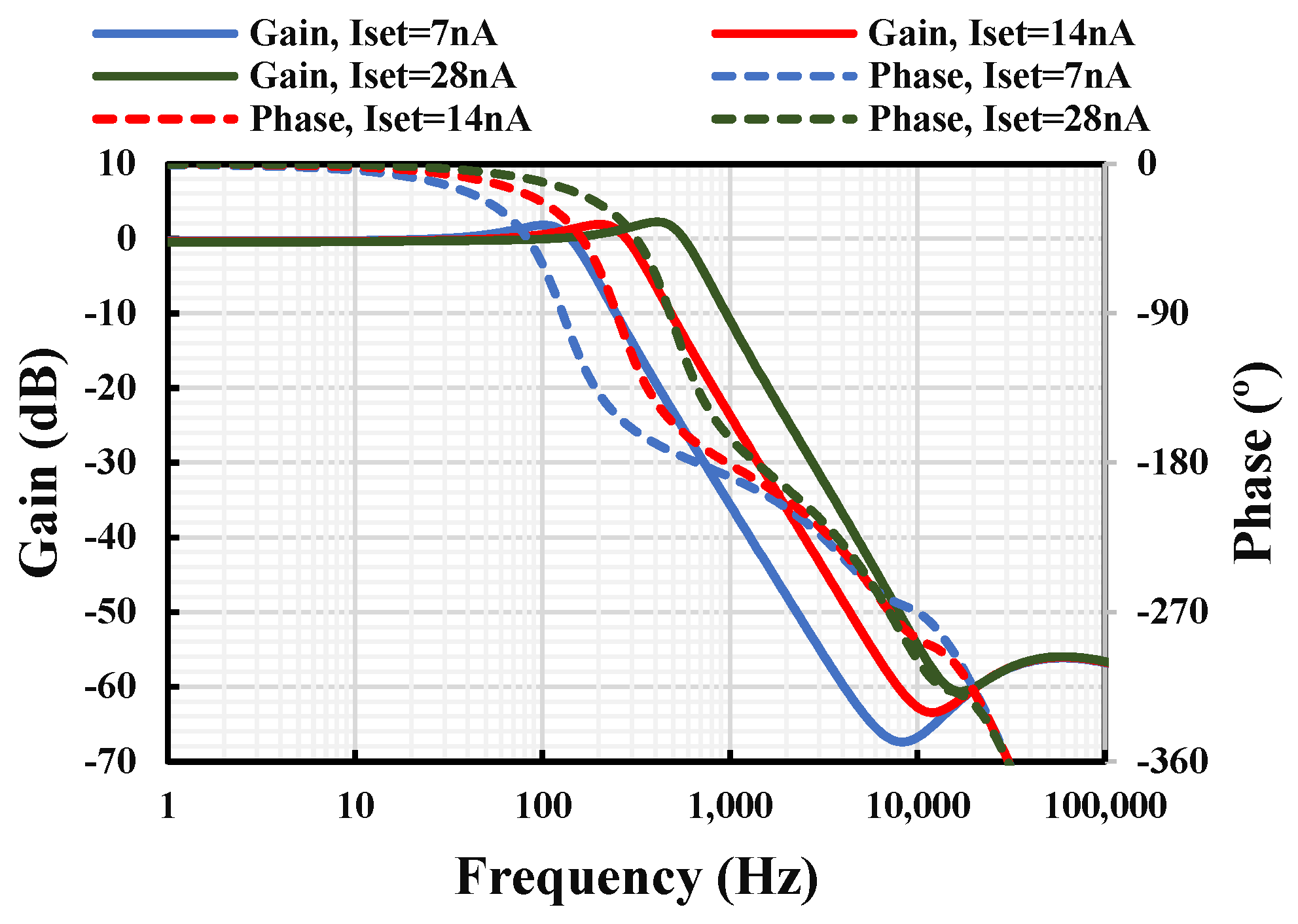
The tuning capability of the filter’s cutoff frequency is demonstrated for the low-pass filter (LPF) in Figure 8. This is achieved with Iset3 = Iset4 = 14 nA and Iset = Iset1 = Iset2 = (7, 14, 28) nA. The corresponding cutoff frequencies are (133.35, 251.18, 501.18) Hz, respectively.
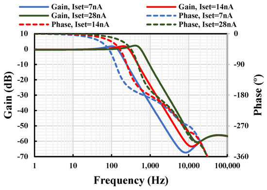
Figure 8.
Filter magnitude and phase responses of the LPF with different setting currents.
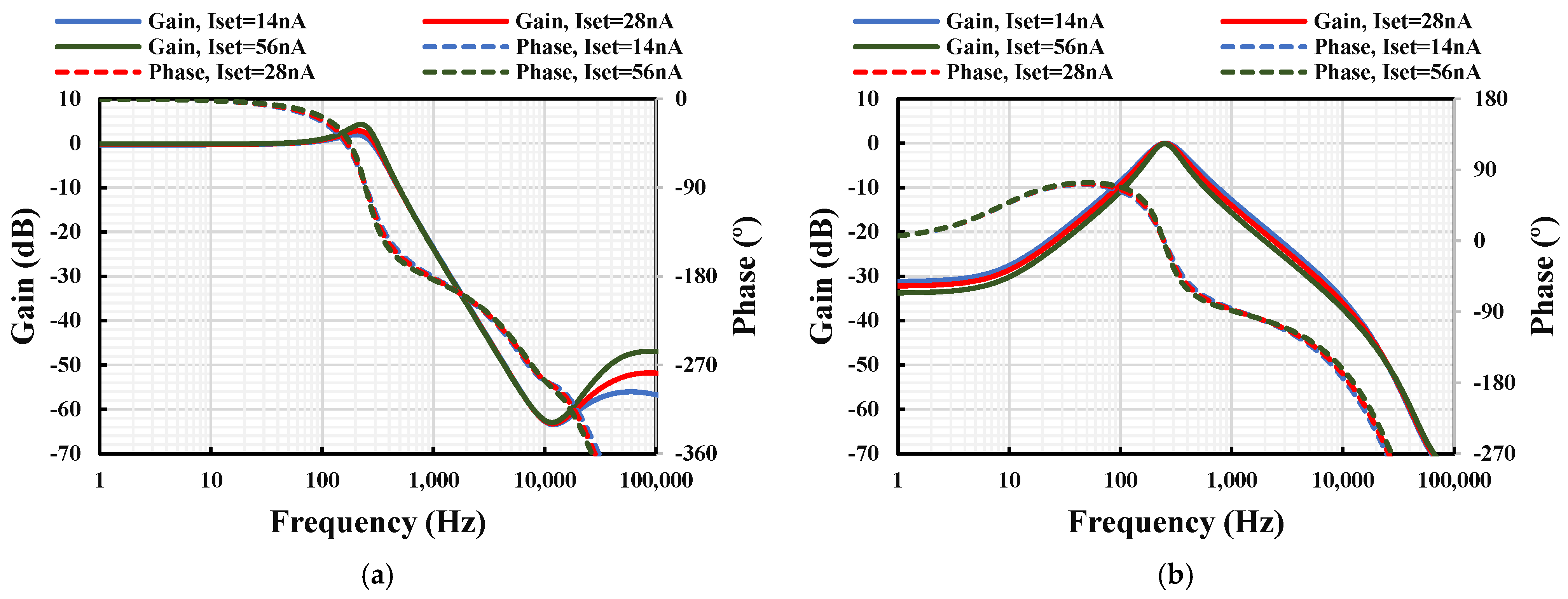
The tuning capability of the filter’s quality factor is demonstrated for both the LPF and BPF in Figure 9. This is achieved with Iset1 = Iset2 = 14 nA and Iset = Iset3 = Iset4 = (14, 28, 56) nA. If the application requires a higher Q factor, it is possible to use a higher resistance value R to achieve this, thereby avoiding an increase in the application’s overall power consumption.
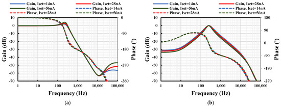
Figure 9.
Filter magnitude and phase responses with setting current Iset = 14 µA for (a) LPF and (b) BPF.
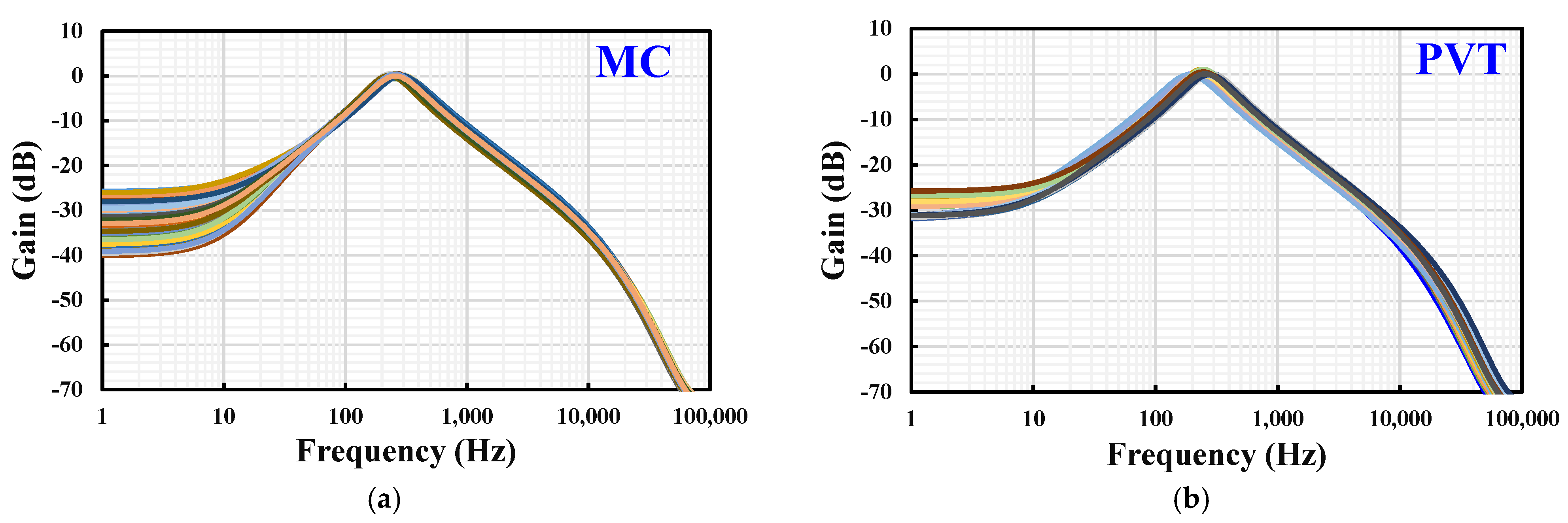
Figure 10 illustrates the filter’s magnitude and phase responses for the BPF under two conditions: (a) Monte Carlo (MC) analysis and (b) process, voltage, and temperature (PVT) analysis. The MC analysis includes 200 runs accounting for process variations and mismatch effects. The PVT analysis encompassed the following:
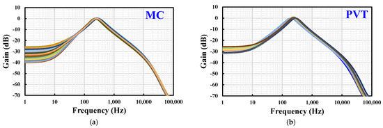
Figure 10.
Filter magnitude and phase responses for BP with (a) MC and (b) PVT analysis.
- -
- Process corner: MOS transistor variations including fast–fast, slow–fast, fast–slow, and slow–slow, along with MIM capacitor variations of fast–fast and slow–slow.
- -
- Voltage corners: ±10% variation in supply voltage.
- -
- Temperature corners: A range from −10 °C to 60 °C.
As evident, the BPF response curves for both MC and PVT analyses overlap, confirming the robustness and reliability of the design under varied conditions.
Table 2 compares the properties of the proposed shadow filter with those of previous works, drawing from recent studies referenced in [22,24,25,27,28]. Unlike these shadow filters, the proposed circuit provides the unique advantage of independently adjusting and without altering the passband gain of the transfer functions. Furthermore, by leveraging the multiple inputs of the DDTA, it achieves both non-inverting and inverting transfer functions for LPF, HPF, BPF, BSF, and APF, covering a total of 10 filtering functions. Although the circuit in [22] can adjust the passband gains using amplifiers, this adjustment is only manual. Compared with [22,24,25,27], the proposed circuit uses lower supply voltage, and consumes less power. Compared to [22,24,25,27], the proposed circuit operates with a lower supply voltage. The voltage-mode circuit in [22] does not provide low-output impedance, while the current-mode circuit in [24] does not provide low-input impedance and uses one floating capacitor. The voltage-mode circuit in [22] lacks low-output impedance, and the current-mode circuit in [24] lacks low-input impedance and uses one floating capacitor. In contrast, the proposed circuit achieves ideal impedance characteristics for voltage-mode operation.
Table 2.
Properties comparison of the proposed shadow filter with those of some previous works.
4. Conclusions
This paper presents an innovative multiple-input single-output shadow filter employing multiple-input DDTAs as active components. The multiple-input capability of the DDTA is achieved through the bulk-driven MOS transistor technique, which eliminates the need for additional MOS differential pairs, thereby reducing power consumption. The DDTA’s design is suitable for processing signals with narrow bandwidths, making it well-suited for biomedical applications like ECG (electrocardiogram) or EEG (electroencephalogram), where the signal frequencies typically lie in the subhertz to 10 kHz range. The low-frequency bandwidth ensures that the DDTA can handle the specific signal characteristics commonly encountered in medical monitoring systems. The proposed filter demonstrates that various filtering functions, including non-inverting and inverting LPF, HPF, BPF, BSF, and APF, can be easily realized by appropriately configuring the input signals. A key advantage of the proposed shadow filter over previous designs is its ability to maintain a constant passband gain across all filtering functions, regardless of changes in the quality factor or natural frequency adjusted by amplifiers. The simulation results confirm the effectiveness and robustness of the proposed filter.
Author Contributions
Conceptualization, M.K., F.K. and T.K.; methodology, M.K., F.K. and T.K.; software, M.K. and F.K.; validation, M.K. and F.K.; formal analysis, M.K. and T.K.; investigation, M.K., F.K. and T.K.; resources, M.K.; data curation, M.K. and F.K.; writing—original draft preparation, M.K., F.K. and T.K.; writing—review and editing, M.K., F.K. and T.K.; visualization, M.K. and F.K.; supervision, M.K. and F.K.; project administration, M.K. and F.K.; funding acquisition, M.K. All authors have read and agreed to the published version of the manuscript.
Funding
This work was supported in part by the University of Defence within the Organization Development Project VAROPS.
Institutional Review Board Statement
Not applicable.
Informed Consent Statement
Not applicable.
Data Availability Statement
Data are contained within the article.
Conflicts of Interest
The authors declare no conflicts of interest.
References
- Lakys, Y.; Fabre, A. Shadow filters-new family of second-order filters. Electron. Lett. 2010, 46, 276–277. [Google Scholar] [CrossRef]
- Lakys, Y.; Fabre, A. Shadow filters generalisation to nth-class. Electron. Lett. 2010, 46, 985–986. [Google Scholar] [CrossRef]
- Abuelma’atti, M.T.; Almutairi, N.R. New current-feedback operational-amplifier based shadow filters. Analog. Integr. Circuits Signal Process. 2016, 86, 471–480. [Google Scholar] [CrossRef]
- Buakaew, S.; Wongtaychatham, C. Boosting the Quality Factor of the Shadow Bandpass Filter. J. Circuits Syst. Comput. 2022, 31, 2250248. [Google Scholar] [CrossRef]
- Varshney, G.; Pandey, N.; Pandey, R. Multi-Functional Fractional-Order Shadow Filter using OTA. In Proceedings of the 2021 Innovations in Power and Advanced Computing Technologies (i-PACT), Kuala Lumpur, Malaysia, 27–29 November 2022; pp. 1–5. [Google Scholar] [CrossRef]
- Khateb, F.; Jaikla, W.; Kulej, T.; Kumngern, M.; Kubanek, D. Shadow filters based on DDCC. IET Circuits Devices Syst. 2017, 11, 631–637. [Google Scholar] [CrossRef]
- Serdar, H. MOSFET-C Shadow Filters Based on FDCCII for Cognitive Communications. J. Circuits Syst. Comput. 2023, 32, 2350137. [Google Scholar] [CrossRef]
- Kumngern, M.; Khateb, F.; Kulej, T. A Novel Multiple-Input Single-Output Current-Mode Shadow Filter and Shadow Oscillator Using Current-Controlled Current Conveyors. Circuits Syst. Signal Process. 2024, 43, 5438–5462. [Google Scholar] [CrossRef]
- Abuelma’atti, M.T.; Almutairi, N. New voltage-mode bandpass shadow filter. In Proceedings of the 2016 13th International Multi-Conference on Systems, Signals & Devices (SSD), Leipzig, Germany, 21–24 March 2016; pp. 412–415. [Google Scholar] [CrossRef]
- Abuelma’atti, M.T.; Almutairi, N.R. New CFOA-based shadow bandpass filter. In Proceedings of the 2016 International Conference on Electronics, Information, and Communications (ICEIC), Danang, Vietnam, 27–30 January 2016; pp. 1–3. [Google Scholar] [CrossRef]
- Anurag, R.; Pandey, R.; Pandey, N.; Singh, M.; Jain, M. OTRA based shadow filters. In Proceedings of the 2015 Annual IEEE India Conference (INDICON), New Delhi, India, 17–20 December 2015; pp. 1–4. [Google Scholar] [CrossRef]
- Alaybeyoglu, E.; Guney, A.; Altun, M.; Mustafa, M.; Kuntman, H. Design of positive feedback driven current-mode amplifiers Z-Copy CDBA and CDTA, and filter applications. Analog. Integr. Circuits Signal Process. 2014, 81, 109–120. [Google Scholar] [CrossRef]
- Pandey, N.; Sayal, A.; Choudhary, R.; Pandey, R. Design of CDTA and VDTA based frequency agile filters. Adv. Electron. 2014, 2014, 176243. [Google Scholar] [CrossRef]
- Atasoyu, M.; Kuntman, H.; Metin, B.; Herencsar, N.; Cicekoglu, O. Design of current-mode class 1 frequency-agile filter employing CDTAs. In Proceedings of the 2015 European Conference on Circuit Theory and Design (ECCTD), Trondheim, Norway, 24–26 August 2015; pp. 1–4. [Google Scholar] [CrossRef]
- Alaybeyoglu, E.; Kuntman, H. A new frequency agile filter structure employing CDTA for positioning systems and secure communications. Analog. Integr. Circuits Signal Process. 2016, 89, 693–703. [Google Scholar] [CrossRef]
- Nand, D.; Pandey, N. New configuration for OFCC-based CM SIMO filter and its application as shadow filter. Arab. J. Sci. Eng. 2018, 43, 3011–3022. [Google Scholar] [CrossRef]
- Alaybeyoglu, E.; Kuntman, H. CMOS implementations of VDTA based frequency agile filters for encrypted communications. Analog. Integr. Circuits Signal Process. 2016, 89, 675–684. [Google Scholar] [CrossRef]
- Buakaew, S.; Narksarp, W.; Wongtaychatham, C. Fully active and minimal shadow bandpass filter. In Proceedings of the 2018 International Conference on Engineering, Applied Sciences, and Technology (ICEAST), Phuket, Thailand, 4–7 July 2018; pp. 1–4. [Google Scholar] [CrossRef]
- Buakaew, S.; Narksarp, W.; Wongtaychatham, C. Shadow bandpass filter with Q-improvement. In Proceedings of the 2019 5th International Conference on Engineering, Applied Sciences and Technology (ICEAST), Luang Prabang, Laos, 2–5 July 2019; pp. 1–4. [Google Scholar] [CrossRef]
- Buakaew, S.; Narksarp, W.; Wongtaychatham, C. High quality-factor shadow bandpass filters with orthogonality to the characteristic frequency. In Proceedings of the 2020 17th International Conference on Electrical Engineering/Electronics, Computer, Telecommunications and Information Technology (ECTI-CON), Phuket, Thailand, 24–27 June 2020; pp. 372–375. [Google Scholar] [CrossRef]
- Chhabra, K.; Singhal, S.; Pandey, N. Realisation of CBTA based current mode frequency agile filter. In Proceedings of the 2019 6th International Conference on Signal Processing and Integrated Networks (SPIN), Noida, India, 7–8 March 2019; pp. 1076–1081. [Google Scholar] [CrossRef]
- Huaihongthong, P.; Chaichana, A.; Suwanjan, P.; Siripongdee, S.; Sunthonkanokpong, W.; Supavarasuwat, P.; Jaikla, W.; Khateb, F. Single-input multiple-output voltage-mode shadow filter based on VDDDAs. AEU-Int. J. Electron. Commun. 2019, 103, 13–23. [Google Scholar] [CrossRef]
- Moonmuang, P.; Pukkalanun, T.; Tangsrirat, W. Voltage differencing gain amplifier-based shadow filter: A comparison study. In Proceedings of the 2020 6th International Conference on Engineering, Applied Sciences and Technology (ICEAST), Chiang Mai, Thailand, 1–4 July 2020; pp. 1–4. [Google Scholar] [CrossRef]
- Singh, D.; Paul, S.K. Realization of current mode universal shadow filter. AEU-Int. J. Electron. Commun. 2020, 117, 153088. [Google Scholar] [CrossRef]
- Singh, D.; Paul, S.K. Improved current mode biquadratic shadow universal filter. Inf. MIDEM 2022, 52, 51–66. [Google Scholar] [CrossRef]
- Singh, D.; Paul, S.K. Mixed-mode universal filter using FD-CCCTA and its extension as shadow filter. Inf. MIDEM 2022, 52, 239–262. [Google Scholar] [CrossRef]
- Singh, D.; Paul, S.K. Realization of multi-mode universal shadow filter and its application as a frequency-hopping filter. Mem.-Mater. Devices Circuits Syst. 2023, 4, 100049. [Google Scholar] [CrossRef]
- Khateb, F.; Kumngern, M.; Kulej, T.; Ranjan, R.K. 0.5 V multiple-input multiple-output differential difference transconductance amplifier and its applications to shadow filter and oscillator. IEEE Access 2023, 11, 31212–31227. [Google Scholar] [CrossRef]
- Kumngern, M.; Khateb, F.; Kulej, T. Shadow filters using multiple-input differential difference transconductance amplifiers. Sensors 2023, 23, 1526. [Google Scholar] [CrossRef]
- Kumngern, M.; Khateb, F.; Kulej, T. 0.5 V Universal Filter and Quadrature Oscillator Based on Multiple-Input DDTA. IEEE Access 2023, 11, 9957–9966. [Google Scholar] [CrossRef]
- Khateb, F.; Kulej, T.; Akbari, M.; Tang, K.-T. A 0.5-V multiple-input bulk-driven OTA in 0.18-μm CMOS. IEEE Trans. Very Large Scale Integr. (VLSI) Syst. 2022, 30, 1739–1747. [Google Scholar] [CrossRef]


Disclaimer/Publisher’s Note: The statements, opinions and data contained in all publications are solely those of the individual author(s) and contributor(s) and not of MDPI and/or the editor(s). MDPI and/or the editor(s) disclaim responsibility for any injury to people or property resulting from any ideas, methods, instructions or products referred to in the content. |
© 2025 by the authors. Licensee MDPI, Basel, Switzerland. This article is an open access article distributed under the terms and conditions of the Creative Commons Attribution (CC BY) license (https://creativecommons.org/licenses/by/4.0/).