
Design and Analysis of 15-Level and 25-Level Asymmetrical Multilevel Inverter Topologies


Abstract

1. Introduction
- A new asymmetrical CHB-based MLI topology that reduces the required number of power semiconductor switches while maintaining high output voltage levels.
- Optimization of the total standing voltage (TSV) and cost function to improve the inverter’s efficiency and affordability.
- A comparative evaluation demonstrating that the proposed topology achieves lower total harmonic distortion (THD) and higher or similar efficiency than existing designs.
2. Proposed Asymmetrical Multilevel Inverters
2.1. DC Sorce Characterization
- Isolated SEPIC Converter: Provides multiple output voltages while maintaining galvanic isolation, enhancing reliability in PV applications.
- Isolated Ćuk Converter: Offers high voltage gain with reduced switching stress, minimizing power losses.
- Flyback Converter: Simple implementation with single-switch control but with limitations in handling high power levels.
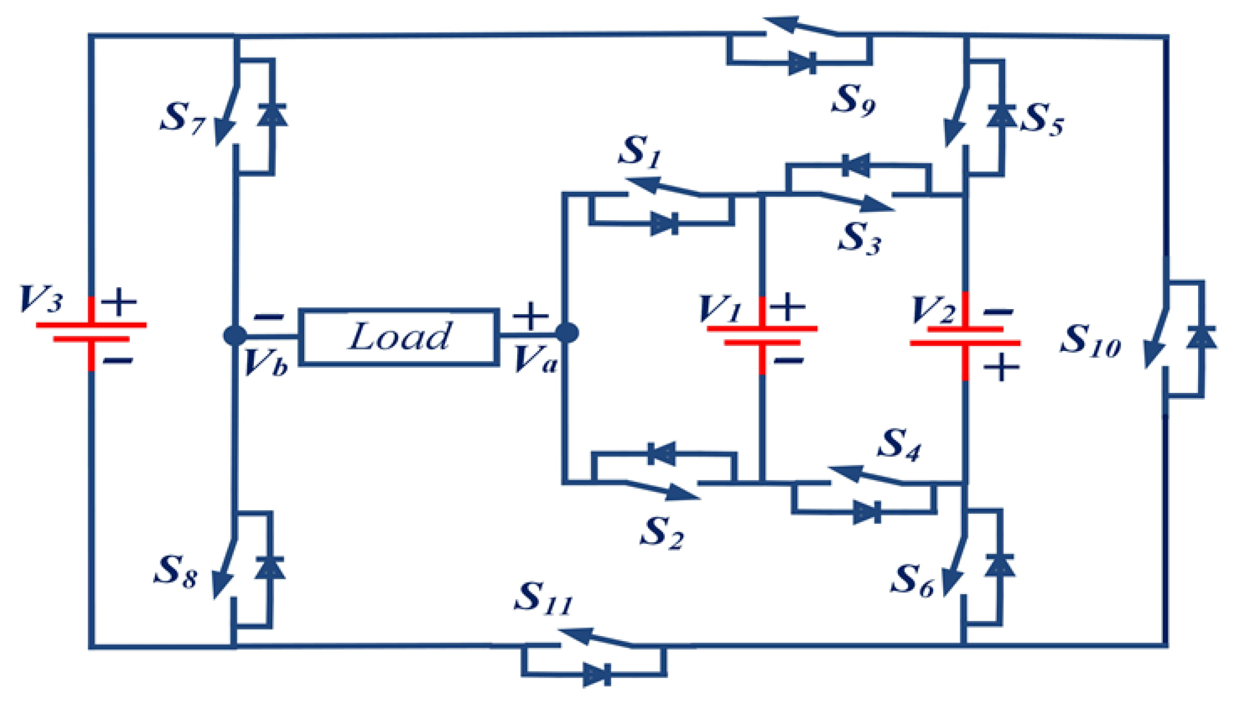
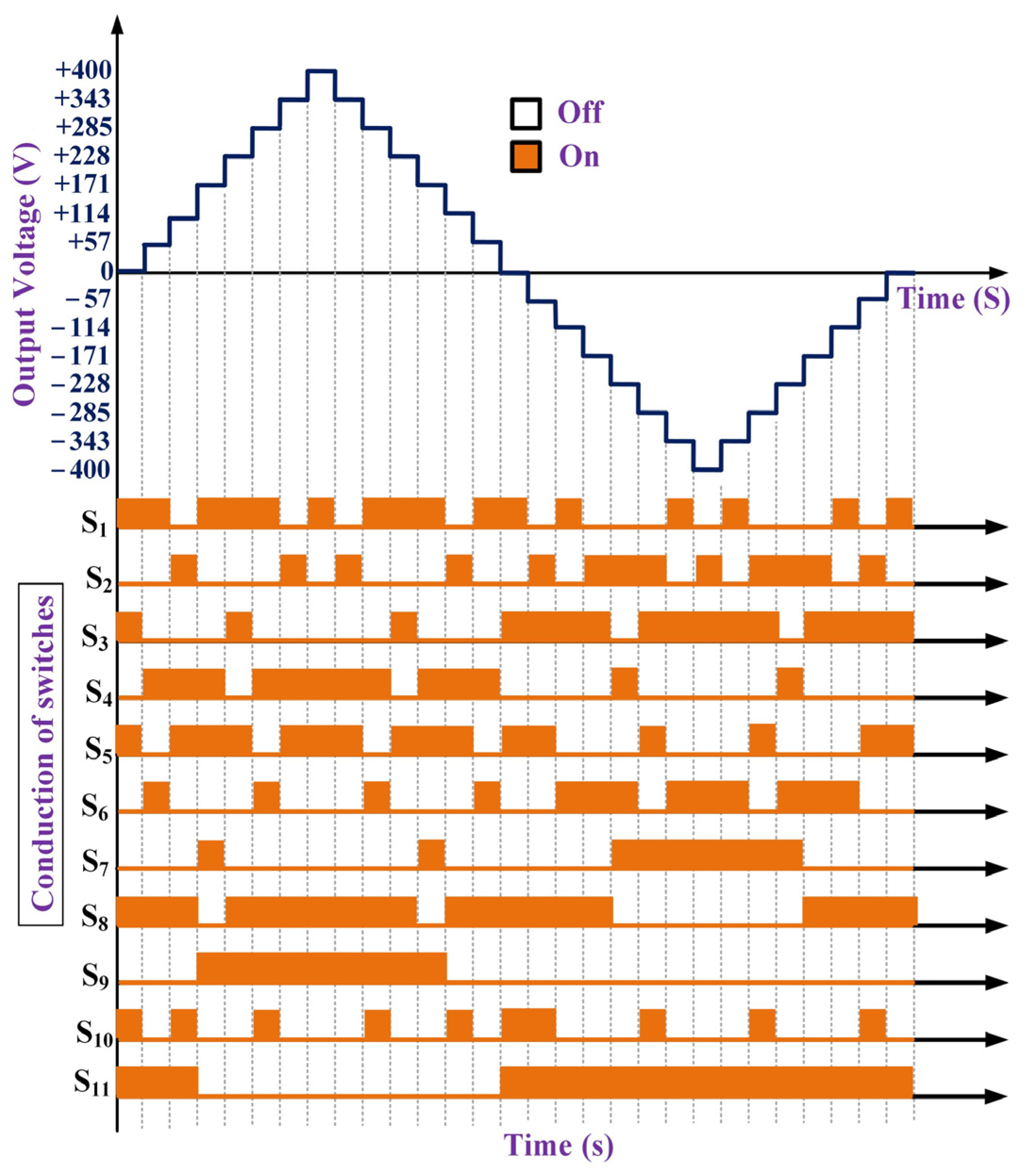
2.2. Asymmetrical 15-Level MLI Topology
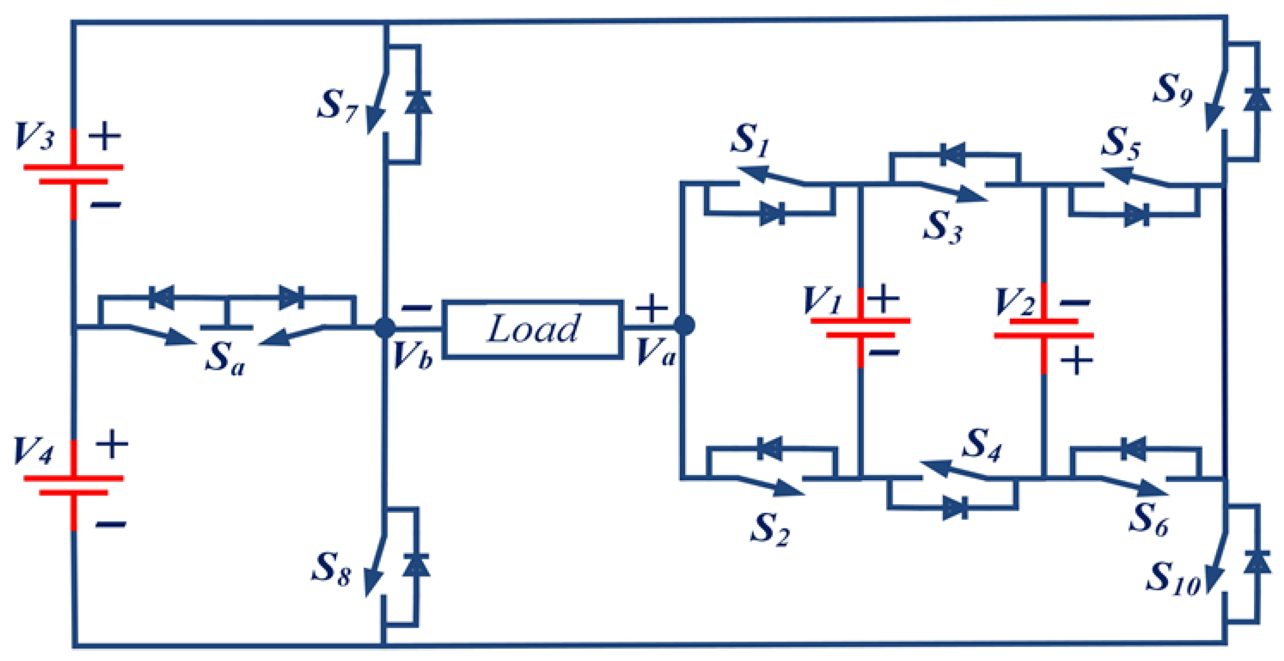
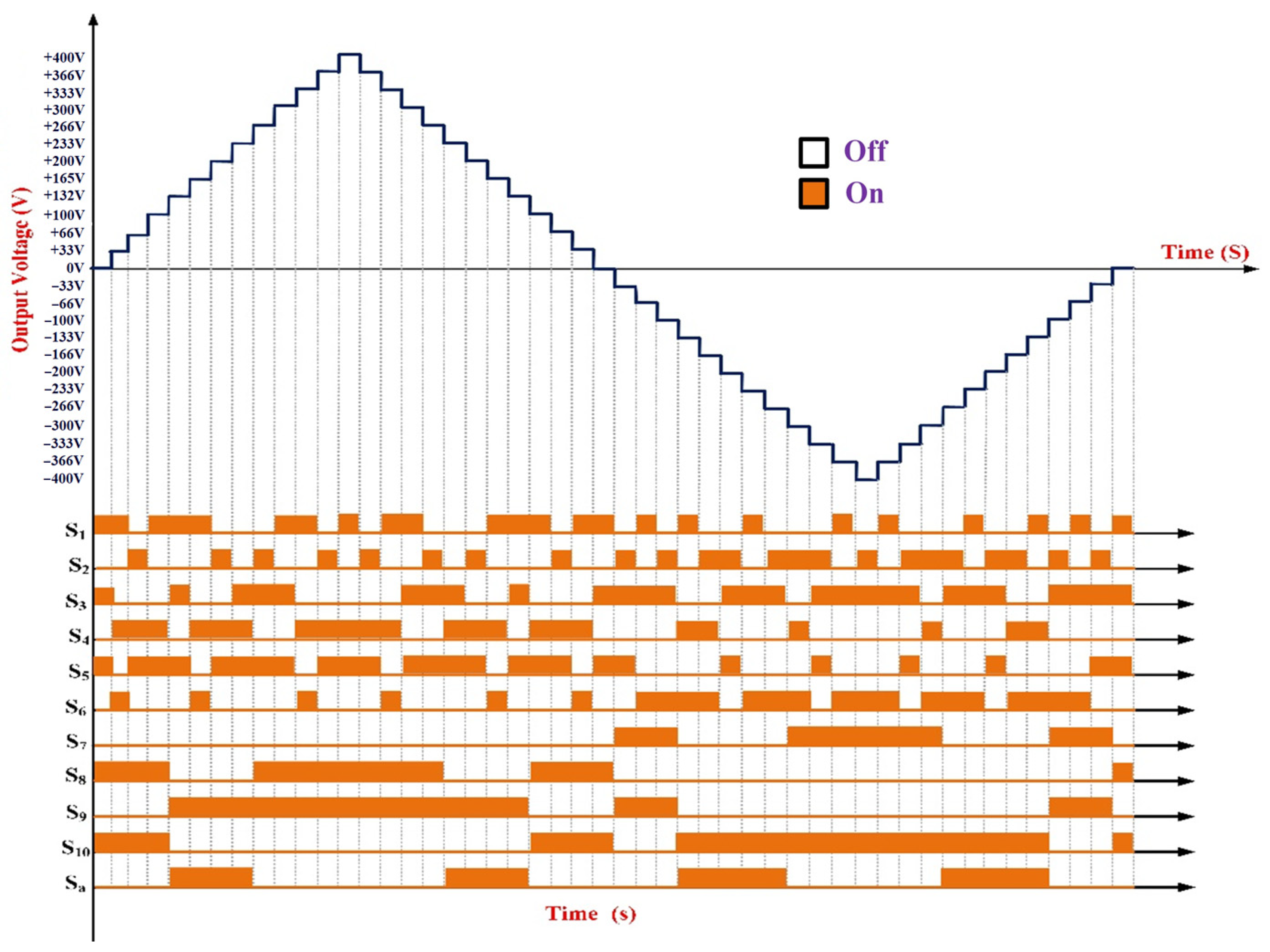
2.3. Asymmetrical 25-Level MLI Topology
3. MLI Performance Evaluation
3.1. Modulation Strategies for Proposed MLIs
- Total Harmonic Distortion (THD): Space vector modulation (SVM) typically provides a lower THD compared to carrier-based PWM methods due to its ability to synthesize the reference voltage vector more effectively.
- Switching Losses: Carrier-based techniques such as Sinusoidal Pulse Width Modulation (SPWM) generally result in higher switching losses, as they require more switch transitions per cycle. SVM, on the other hand, optimizes switching sequences, reducing energy dissipation.
- Computational Complexity: While SVM offers superior harmonic performance and lower losses, it requires higher computational resources, making it more challenging to implement in real-time embedded control systems.
3.2. Total Standing Voltage and Component Count per Level Factor
3.2.1. TSV of 15-Level MLI
MBVS2 = V1 = 1·VOstep-15
MBVS3 = V1 + V2 = 3·VOstep-15
MBVS4 = V2 + V1 = 3·VOstep-15
MBVS5 = V2 = 2·VOstep-15
MBVS6 = V2 = 2·VOstep-15
MBVS7 = V3 = 4·VOstep-15
MBVS8 = V3 = 4·VOstep-15
MBVS9 = V1 = 1·VOstep-15
MBVS10 = V2 = 2·VOstep-15
MBVS11 = V1 = 1·VOstep-15
3.2.2. TSV of 25-Level MLI
MBVS2 = V1 = 1·VOstep-25
MBVS3 = V1 + V2 = 3·VOstep-25
MBVS4 = V1 + V2 = 3·VOstep-25
MBVS5 = V2 = 2·VOstep-25
MBVS6 = V2 = 2·VOstep-25
MBVS7 = V3 = 4·VOstep-25
MBVS8 = V4 = 5·VOstep-25
MBVS9 = V2 = 2·VOstep-25
MBVS10 = V2 = 2·VOstep-25
3.3. Component Count per Level Factor
3.4. Cost Functions
3.5. Power Loss and Efficiency
4. Comparative Studies
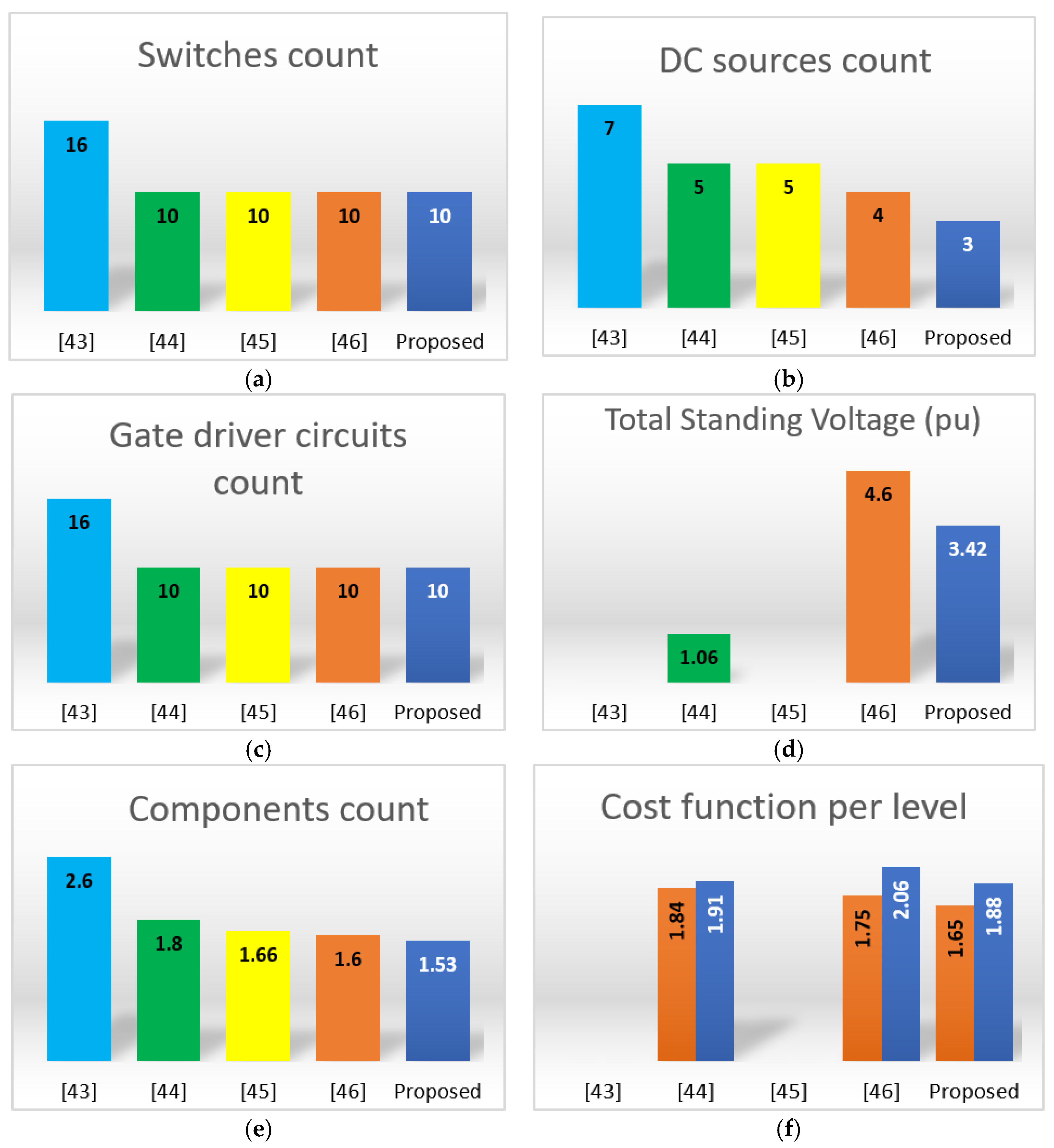
4.1. Comparative with the Proposed 15-Level MLI
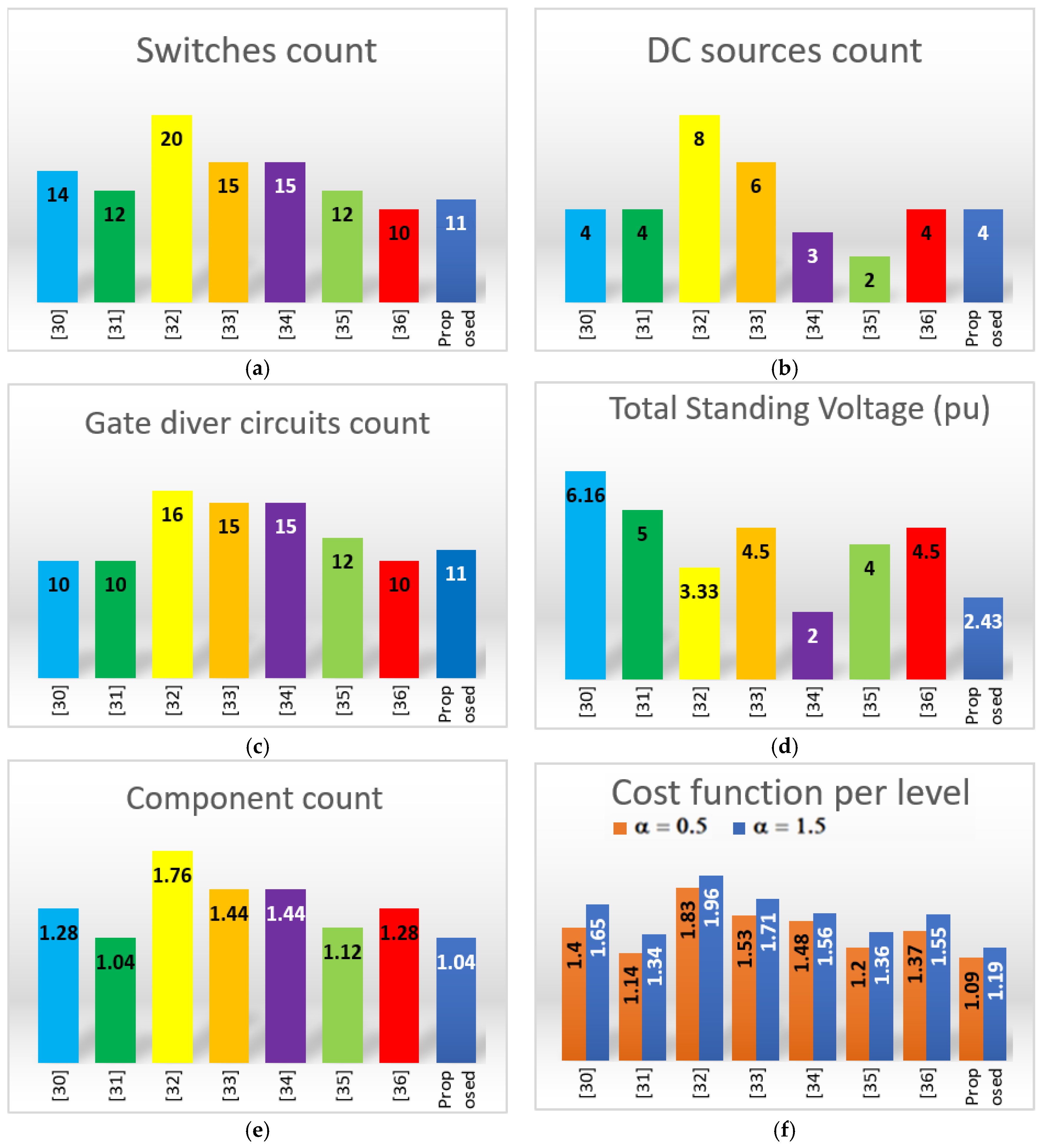
4.2. Comparative with the Proposed 25-Level MLI
4.3. Considerations on the Design Optimization of the Proposed MLIs
- Economic Viability: While reducing TSV can enhance reliability, it often requires additional components or more expensive semiconductor switches with higher voltage ratings. This increases manufacturing costs, making the inverter less attractive for cost-sensitive applications such as renewable energy systems and residential power converters.
- Component Count Reduction: A lower TSV often necessitates additional capacitors, diodes, or switch redundancy, which would increase the overall component count. Keeping the number of components low is critical for simplified circuit design, ease of maintenance, and reduced failure rates.
- Scalability and Practical Implementation: Minimizing the cost function ensures that the proposed MLI remains scalable for various voltage levels. By striking a balance between TSV and cost, the topology can be adapted for medium- and high-power applications without significantly increasing complexity.
- Operational Efficiency: Although TSV reduction can lower stress on switches, proper control strategies (such as optimized PWM techniques and switching schemes) mitigate excessive voltage stress without requiring additional components.
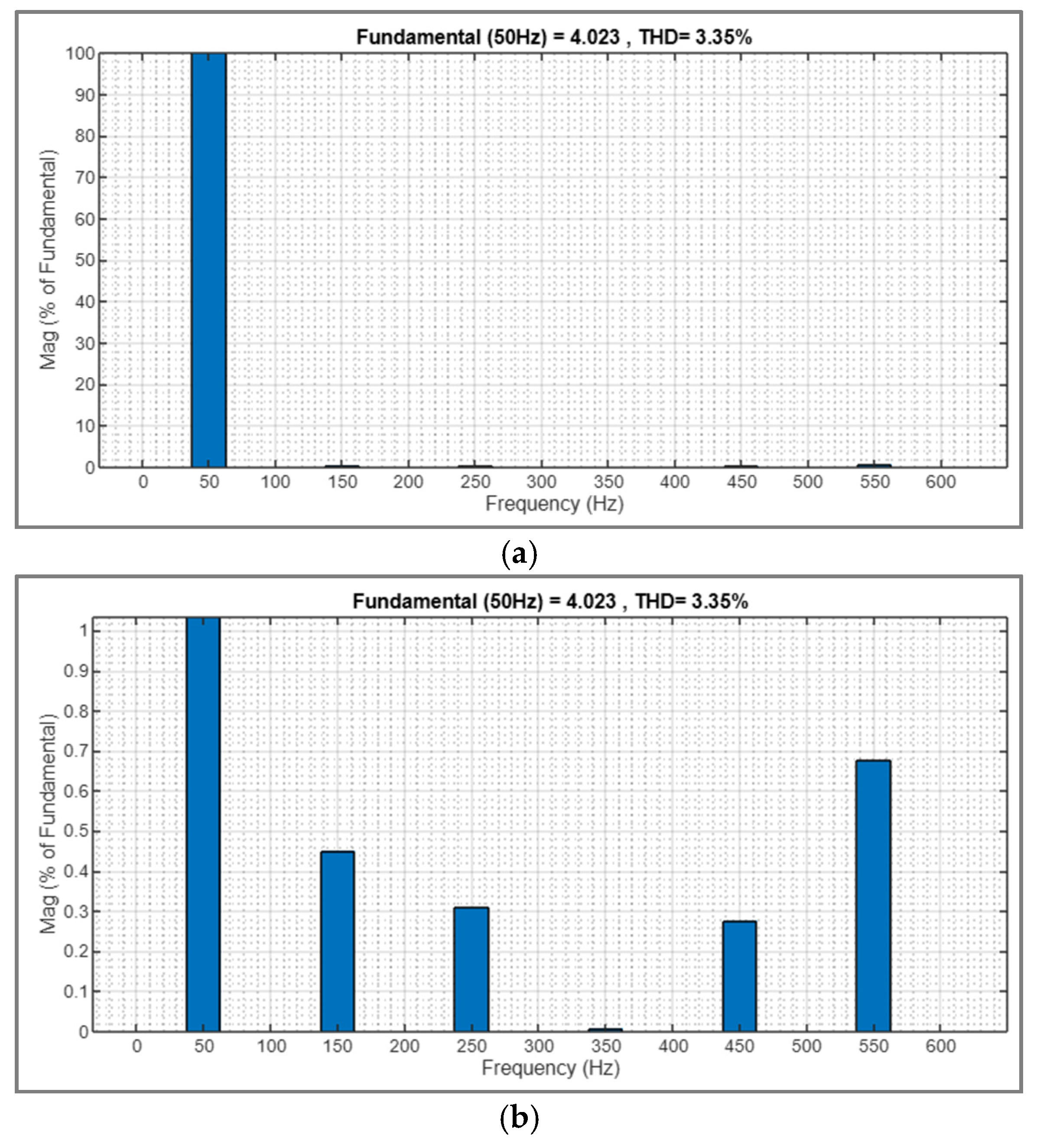
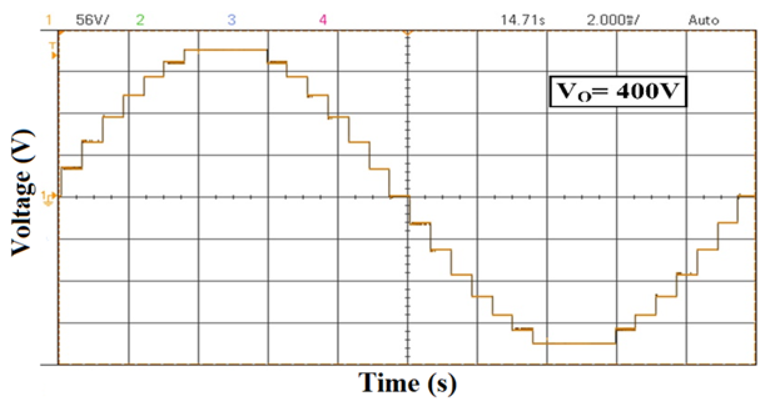
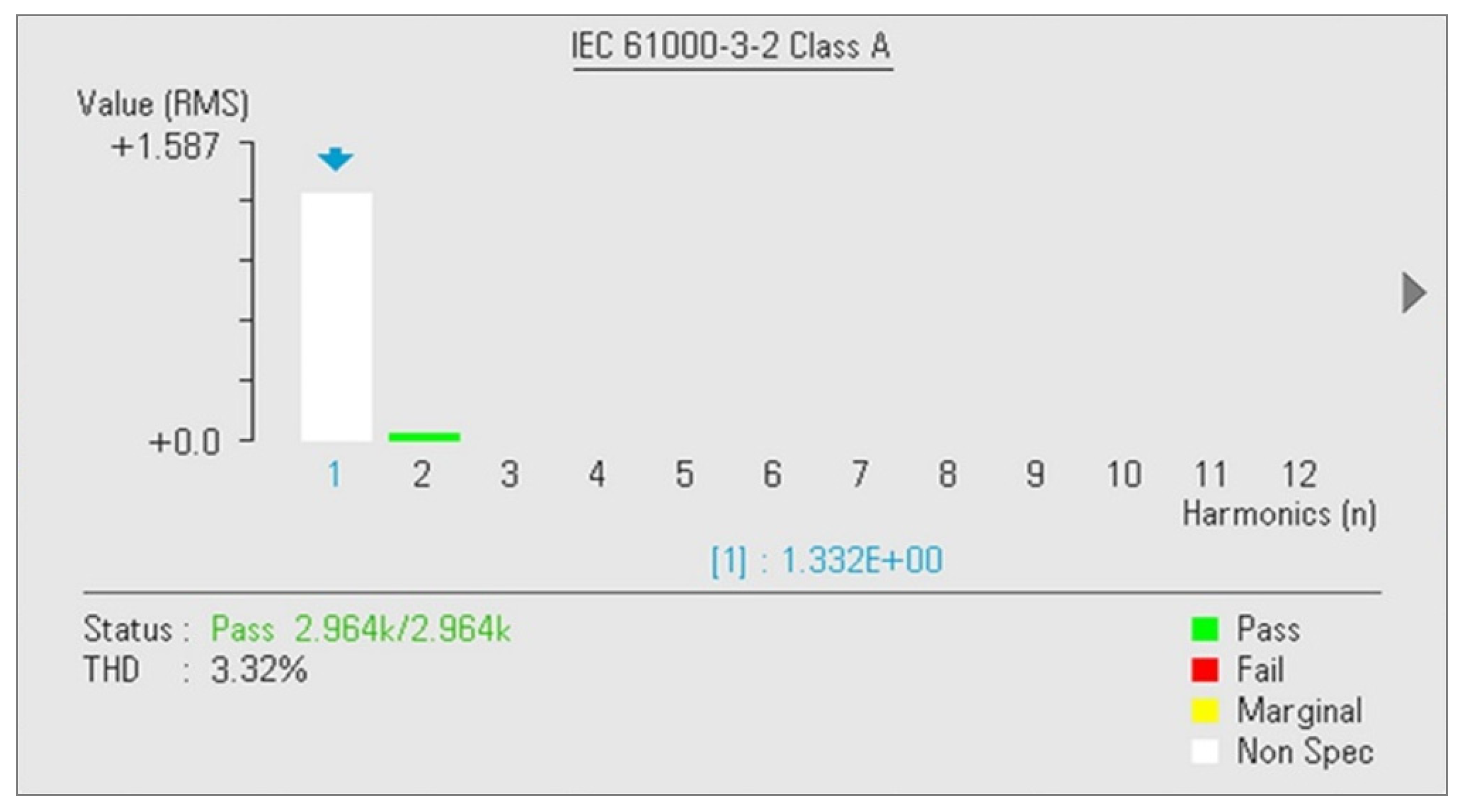
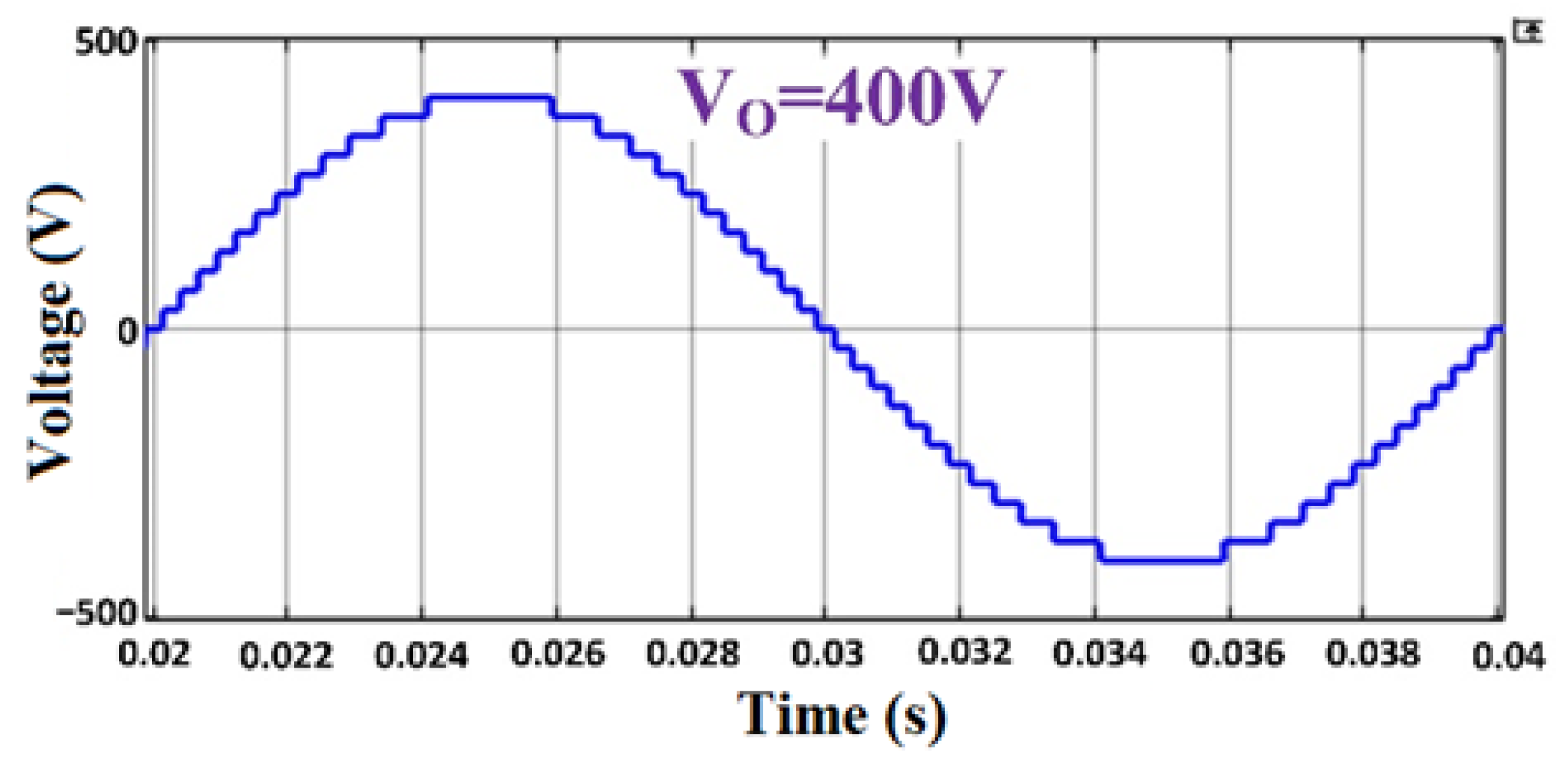
5. Simulation and Experimental Results
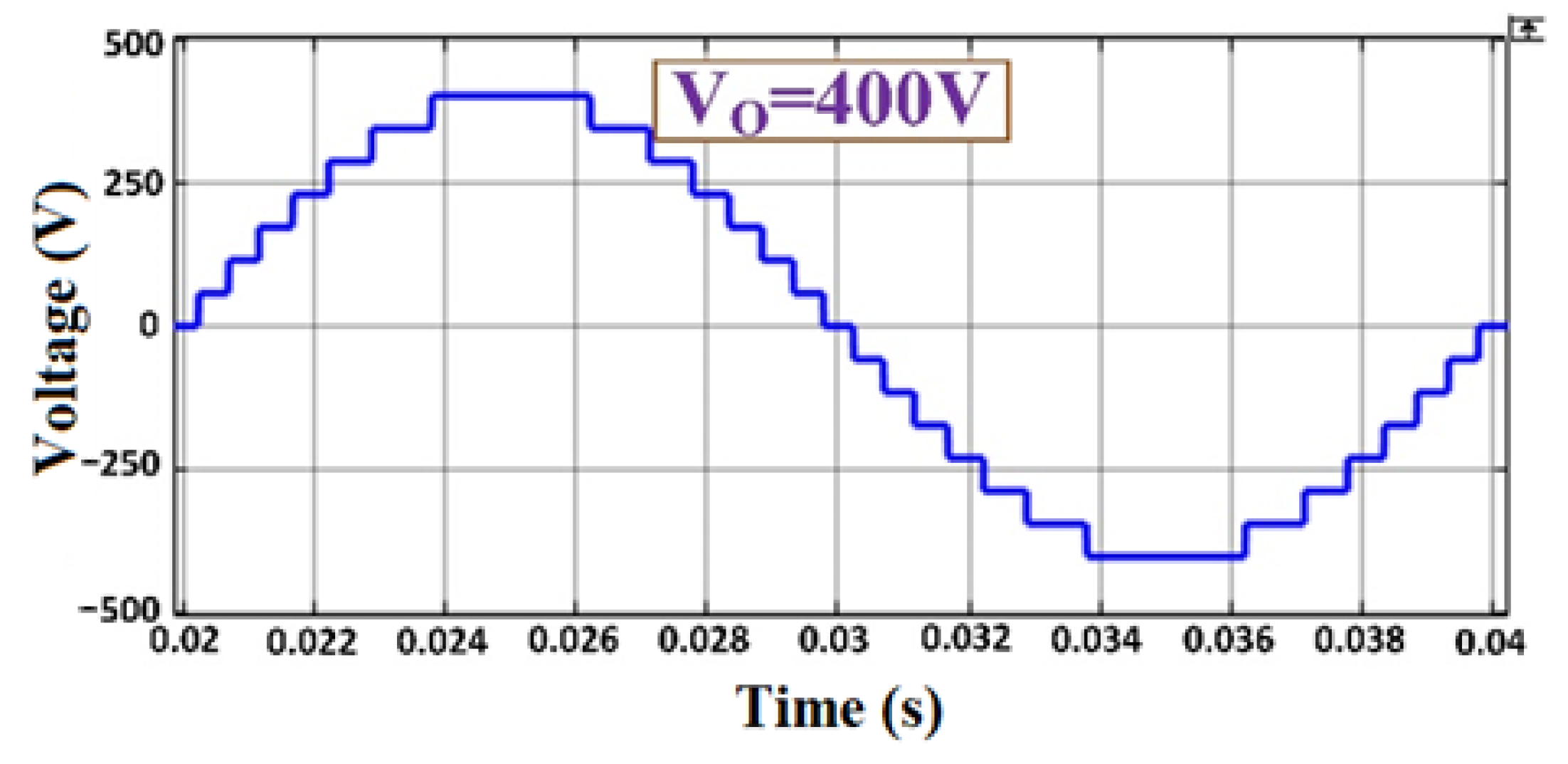
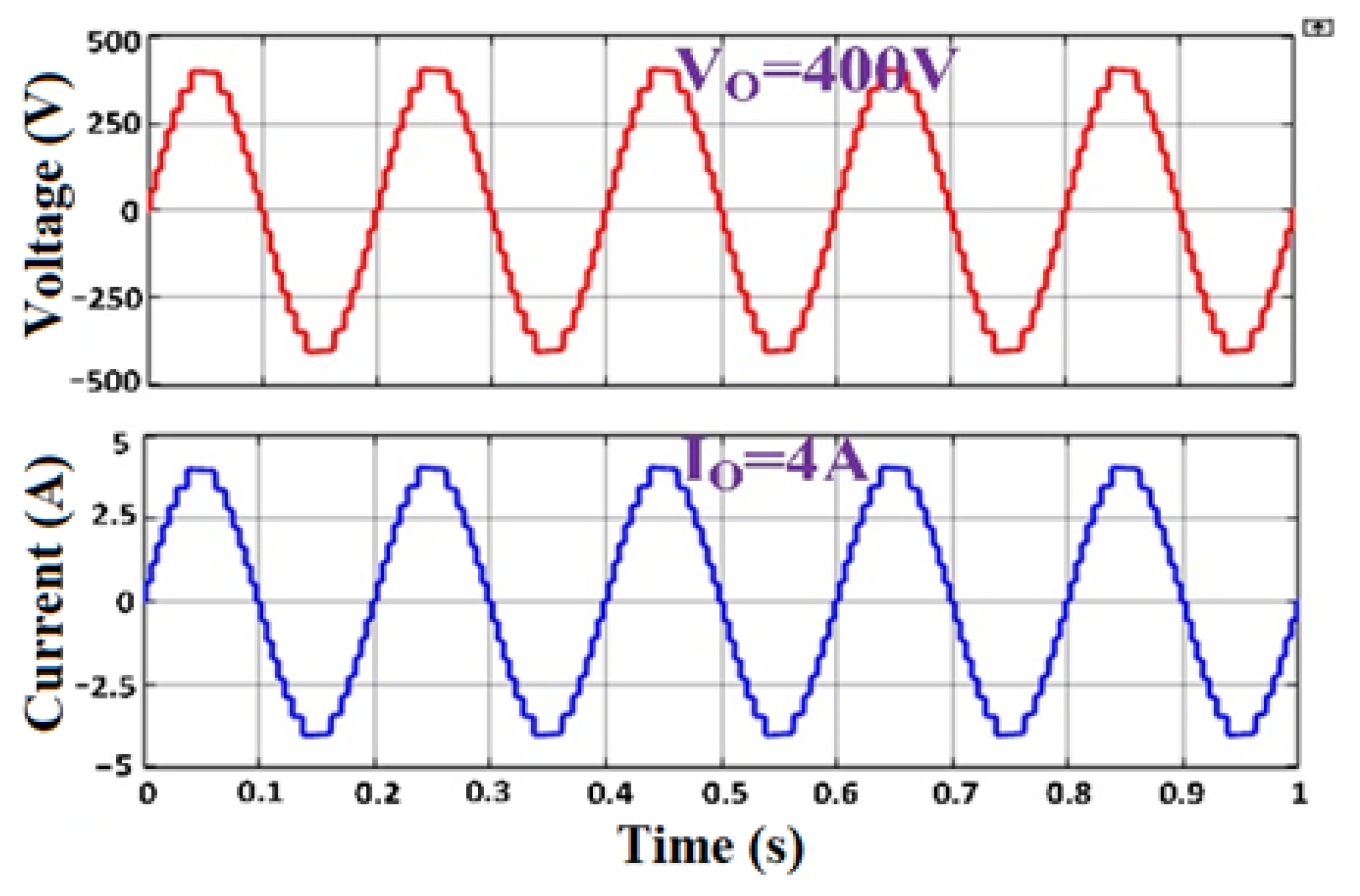
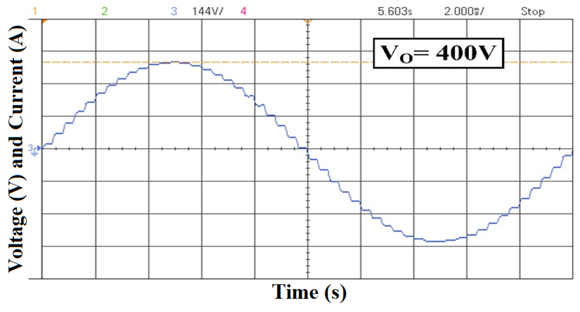
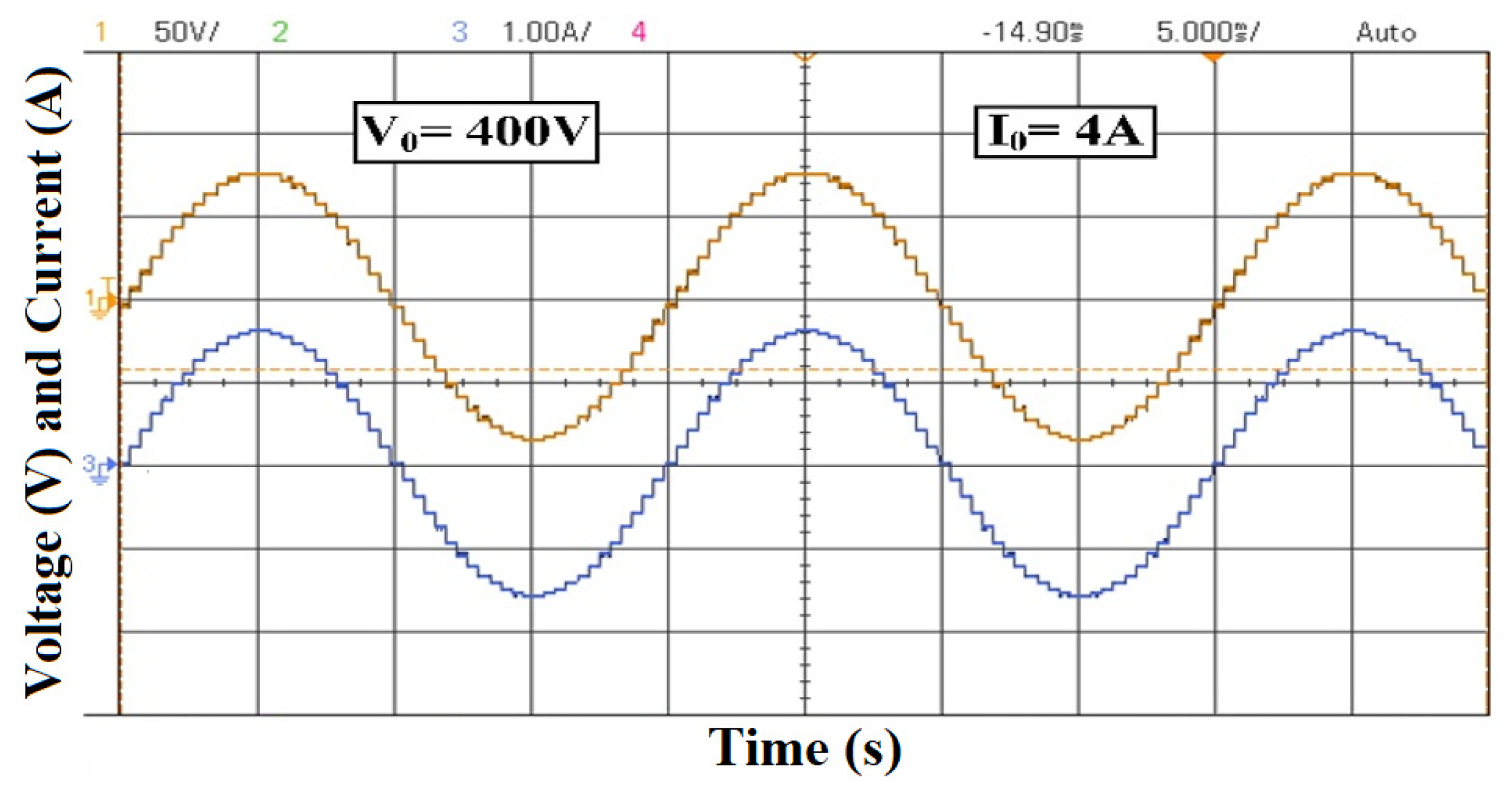
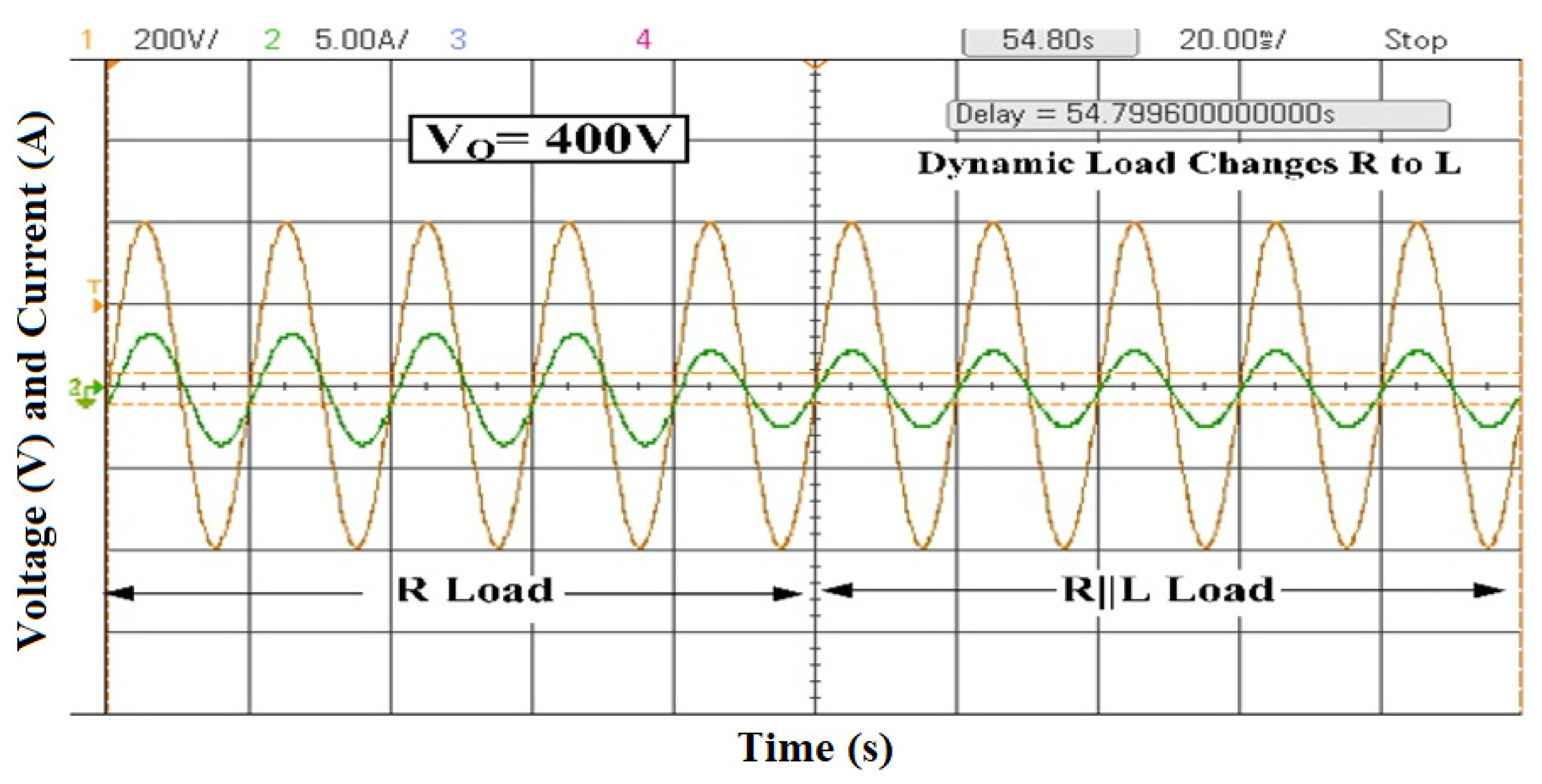
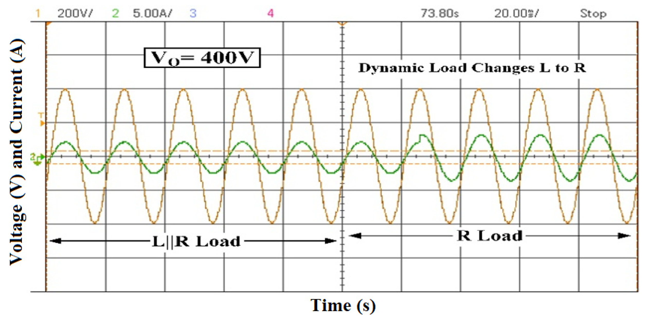
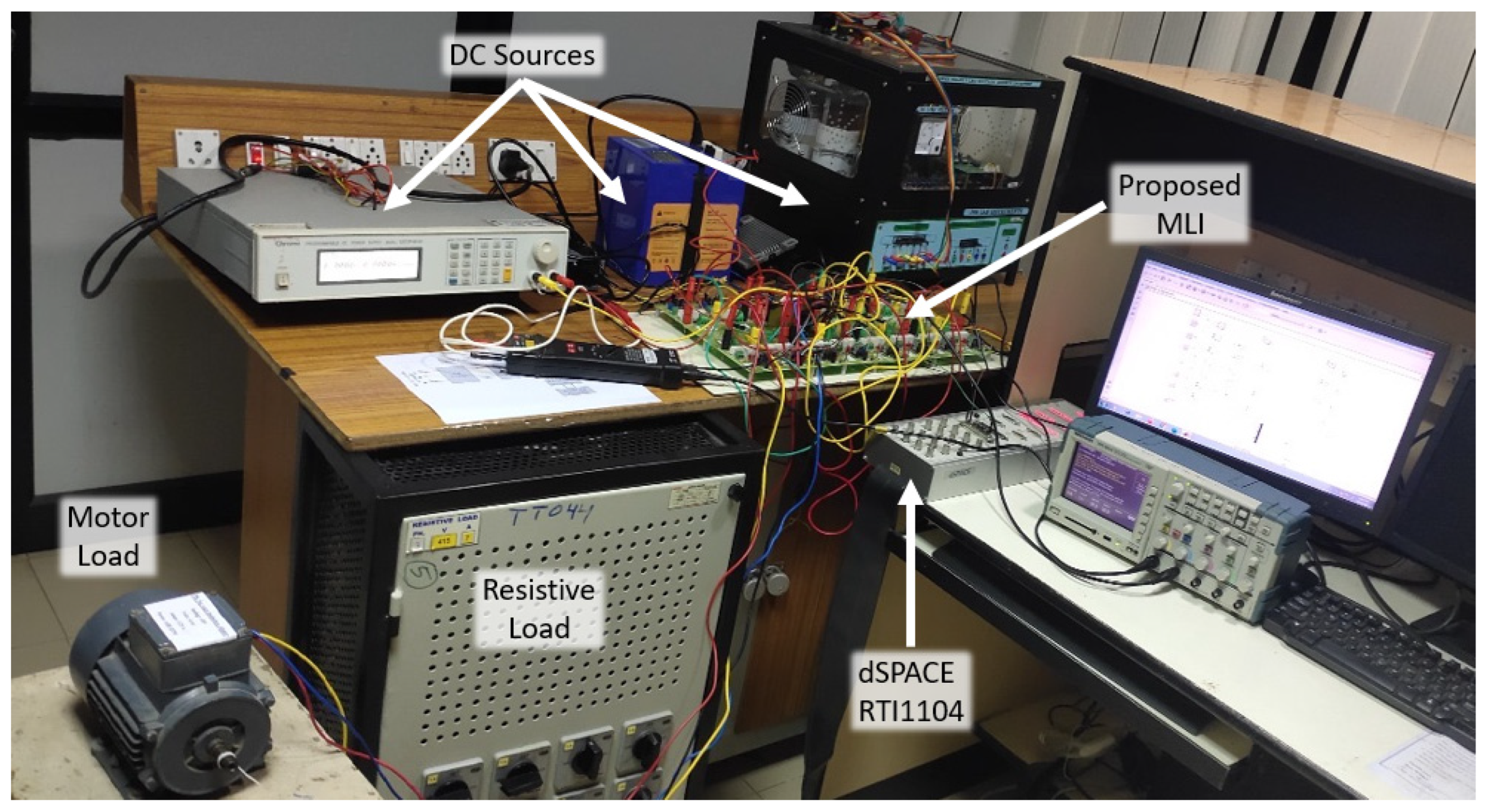
5.1. Simulation and Test of the Proposed 15-Level MLI
- Programmable DC Power Supply: 600 V, 10 A, Model N8900 Series, Keysight Technologies, Colorado Spring, CO, USA.
- Multiple isolated DC voltage sources configured for asymmetrical voltage levels per MLI requirements.
- IGBT Modules: 600 V, 75 A, Model CM75DU-12, Powerex Inc., Philadelphia, PA, USA.
- Gate Driver ICs for IGBT triggering: 1ED020I12-F2, Infineon Technologies, Munich, Germany.
- Optocouplers for isolation between control and power circuits: TLP250, Toshiba Electronic Devices & Storage Corporation, Tokyo, Japan.
- Control Unit:
- Real-time interface controller: RTI1104, dSPACE, Paderborn, Germany. Interfaced with MATLAB/Simulink.
- PWM generation and switching signal control using predefined switching angles.
- DSP/FPGA-based implementation for high-speed computation and real-time data acquisition.
- Oscilloscope: 200 MHz, 2 GS/s, Model TDS 2024B, Tektronix, Bracknell, UK. Used for analysis of output voltage and switching signal.
- Load Configuration:
- Resistive Load: 100 Ω high-power resistor (10 kW rated).
- Inductive Load: Motor load with L = 98 mH, R ≈ 50 Ω.
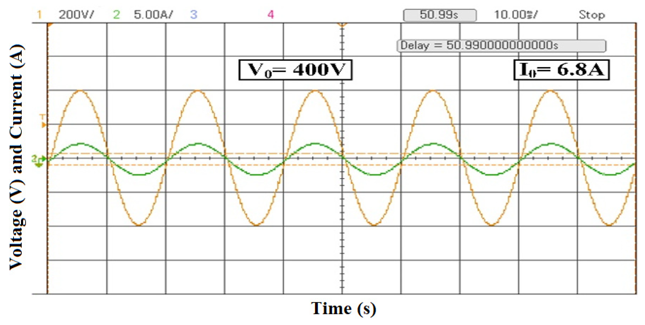
5.2. Simulation and Test of the Proposed 25-Level MLI
5.3. Power Losses and Efficiency Estimation in the Proposed MLIs
6. Conclusions
Author Contributions
Funding
Data Availability Statement
Acknowledgments
Conflicts of Interest
References
- Zhou, Y.; Li, H. Analysis and suppression of leakage current in cascaded-multilevel-inverter-based PV systems. IEEE Trans. Power Electron. 2013, 29, 5265–5277. [Google Scholar] [CrossRef]
- Das, M.K.; Jana, K.C.; Akanksha, S. Performance evaluation of an asymmetrical reduced switched multi-level inverter for a grid-connected PV system. IET Renew. Power Gener. 2013, 12, 252–263. [Google Scholar] [CrossRef]
- Jain, S.; Venu, S. A highly efficient and reliable inverter configuration based cascaded multilevel inverter for PV systems. IEEE Trans. Ind. Electron. 2016, 64, 2865–2875. [Google Scholar]
- Wang, K.; Li, Y.; Zheng, Z.; Xu, L. Voltage balancing and fluctuation suppression methods of floating capacitors in a new modular multilevel converter. IEEE Trans. Ind. Electron. 2013, 60, 1943–1954. [Google Scholar]
- Babaei, E.; Hosseini, S.H. Charge balance control methods for asymmetrical cascade multilevel converters. In Proceedings of the 2007 International Conference on Electrical Machines and Systems (ICEMS), Seoul, Republic of Korea, 8–11 October 2007; pp. 74–79. [Google Scholar]
- Ebrahimi, J.; Babaei, E.; Gharehpetian, G.B. A new topology of cascaded multilevel converters with reduced number of components for high-voltage applications. IEEE Trans. Power Electron. 2011, 26, 3109–3118. [Google Scholar]
- Rahim, N.A.; Elias, M.F.M.; Hew, W.P. Transistor clamped H-bridge based cascaded multilevel inverter with new method of capacitor voltage balancing. IEEE Trans. Ind. Electron. 2013, 60, 2943–2956. [Google Scholar]
- Alonge, F.; Busacca, A.; Calabretta, M.; D’Ippolito, F.; Fagiolini, A.; Garraffa, G.; Messina, A.A.; Sferlazza, A.; Stivala, S. Nonlinear Robust Control of a Quadratic Boost Converter in a Wide Operation Range, Based on Extended Linearization Method. Electronics 2022, 11, 2336. [Google Scholar] [CrossRef]
- Murad, Z.; Anzi, F.A.; Ben-Brahim, L. A Comparative Study of High-gain Cascaded DC-DC Converter Topologies. In Proceedings of the 2022 3rd International Conference on Smart Grid and Renewable Energy (SGRE), Doha, Qatar, 20–22 March 2022; pp. 1–6. [Google Scholar] [CrossRef]
- Manjrekar, M.D.; Lipo, T.A. A hybrid multilevel inverter topology for drive applications. In Proceedings of the APEC ’98 Thirteenth Annual Applied Power Electronics Conference and Exposition, Anaheim, CA, USA, 15–19 February 1998; Volume 2, pp. 523–529. [Google Scholar]
- Kouro, S.; Malinowski, M.; Gopakumar, K.; Pou, J.; Franquelo, L.G.; Wu, B.; Rodriguez, J.; Pérez, M.A.; Leon, J.I. Recent advances and industrial applications of multilevel converters. IEEE Trans. Ind. Electron. 2010, 57, 2553–2580. [Google Scholar]
- Levi, E. Advances in converter control and innovative exploitation of additional degrees of freedom for multiphase machines. IEEE Trans. Ind. Electron. 2016, 63, 433–448. [Google Scholar] [CrossRef]
- Mokhberdoran, A.; Ajami, A. Symmetric and asymmetric design and implementation of new cascaded multilevel inverter topology. IEEE Trans. Power Electron. 2014, 29, 6712–6724. [Google Scholar]
- Hosseinzadeh, M.A.; Sarbanzadeh, M.; Sarbanzadeh, E.; Rivera, M.; Gregor, R. Back-to-Back modified T-Type half-bridge module for cascaded multi-level inverters with decreased number of components. In Proceedings of the IEEE International Conference on Electrical Systems for Aircraft, Railway, Ship Propulsion and Road Vehicles & International Transportation Electrification Conference (ESARS-ITEC), Nottingham, UK, 7–9 November 2018; pp. 6–11. [Google Scholar]
- Babaei, E.; Hosseini, S.H.; Gharehpetian, G.B.; Haque, M.T.; Sabahi, M. Reduction of DC voltage sources and switches in asymmetrical multilevel converters using a novel topology. Electr. Power Syst. Res. 2007, 77, 1073–1085. [Google Scholar] [CrossRef]
- Mekhilef, S.; Kadir, M.N.A. Voltage control of three-stage hybrid multilevel inverter using vector transformation. IEEE Trans. Power Electron. 2010, 25, 2599–2606. [Google Scholar] [CrossRef]
- RAlishah, S.; Nazarpour, D.; Hosseini, S.H.; Sabahi, M. New hybrid structure for multilevel inverter with fewer number of components for highvoltage levels. IET Power Electron. 2014, 7, 96–104. [Google Scholar] [CrossRef]
- Karasani, R.R.; Borghate, V.B.; Meshram, P.M.; Suryawanshi, H.M.; Sabyasachi, S. A three-phase hybrid cascaded modular multilevel inverter for renewable energy environment. IEEE Trans. Power Electron. 2017, 32, 1070–1087. [Google Scholar] [CrossRef]
- Odeh, C.I.; Obe, E.S.; Ojo, O. Topology for cascaded multilevel inverter. IET Power Electron. 2016, 9, 921–929. [Google Scholar] [CrossRef]
- Banaei, M.R.; Oskuee, M.R.J.; Khounjahan, H. Recon_guration of semi-cascaded multilevel inverter to improve systems performance parameters. IET Power Electron. 2014, 7, 1106–1112. [Google Scholar] [CrossRef]
- Ali, J.S.M.; Kannan, R. A new symmetric cascaded multilevel inverter topology using single and double source unit. J. Power Electron. 2015, 15, 951–963. [Google Scholar]
- Dhanamjayulu, C.; Arunkumar, G.; Pandian, B.J.; Padmanaban, S. Design and implementation of a novel asymmetrical multilevel inverter optimal hardware components. Int. Trans. Electr. Energy Syst. 2020, 30, e12201. [Google Scholar] [CrossRef]
- Dhanamjayulu, C.; Meikandasivam, S. Performance veri_cation of symmetric hybridized cascaded multilevel inverter with reduced number of switches. In Proceedings of the 2017 Innovations in Power and Advanced Computing Technologies (i-PACT), Vellore, India, 21–22 April 2017; pp. 1–5. [Google Scholar]
- Ali, J.S.M.; Krishnaswamy, V. An assessment of recent multilevel inverter topologies with reduced power electronics components for renewable applications. Renew. Sustain. Energy Rev. 2018, 82, 3379–3399. [Google Scholar]
- Dhanamjayulu, C.; Sanjeevikumar, P.; Palanisamy, K.; Blaabjerg, F.; Maroti, P.K. A novel nine and seventeen-step multilevel inverters with condensed switch count. In Proceedings of the IEEE 21st Workshop Control Modeling Power Electron (COMPEL), Aalborg, Denmark, 9–12 November 2020; pp. 1–6. [Google Scholar]
- Suresh, Y.; Venkataramanaiah, J.; Panda, A.K.; Dhanamjayulu, C.; Venugopal, P. Investigation on cascade multilevel inverter with symmetric, asymmetric, hybrid and multi-cell configurations. Ain Shams Eng. J. 2017, 8, 263–276. [Google Scholar] [CrossRef]
- Suresh, Y.; Panda, A.K. Investigation on hybrid cascaded multilevel inverter with reduced dc sources. Renew. Sustain. Energy Rev. 2013, 26, 49–59. [Google Scholar] [CrossRef]
- Dhanamjayulu, C.; Meikandasivam, S. Implementation and comparison of symmetric and asymmetric multilevel inverters for dynamic loads. IEEE Access 2018, 6, 738–746. [Google Scholar] [CrossRef]
- Prabaharan, N.; Fathima, A.H.; Palanisamy, K. New hybrid multilevel inverter topology with reduced switch count using carrier based pulse width modulation technique. In Proceedings of the 2015 IEEE Conference on Energy Conversion (CENCON), Johor Bahru, Malaysia, 19–20 October 2015; pp. 176–180. [Google Scholar]
- Alishah, R.S.; Hosseini, S.H.; Babaei, E.; Sabahi, M.; Ghare-hkoushan, A.Z. Optimal design of new cascade multilevel converter topology based on series connection of extended sub-multilevel units. IET Power Electron. 2016, 9, 1341–1349. [Google Scholar] [CrossRef]
- Alishah, R.S.; Hosseini, S.H.; Babaei, E.; Sabahi, M. A new general multilevel converter topology based on cascaded connection of sub multilevel units with reduced switching components, DC sources, and blocked voltage by switches. IEEE Trans. Ind. Electron. 2016, 63, 7157–7164. [Google Scholar] [CrossRef]
- Samadaei, E.; Gholamian, S.A.; Sheikholeslami, A.; Adabi, J. An envelope type (E-Type) module: Asymmetric multilevel inverters with reduced components. IEEE Trans. Ind. Electron. 2016, 63, 7148–7156. [Google Scholar] [CrossRef]
- Ali, J.S.M.; Alishah, R.S.; Sandeep, N.; Hosseini, S.H.; Babaei, E.; Vijayakumar, K.; Yaragatti, U.R. A new generalized multilevel converter topology based on cascaded connection of basic units. IEEE J. Emerg. Sel. Top. Power Electron. 2019, 7, 2498–2512. [Google Scholar]
- Chappa, A.; Gupta, S.; Sahu, L.K.; Gautam, S.P.; Gupta, K.K. Symmetrical and asymmetrical reduced device multilevel inverter topology. IEEE J. Emerg. Sel. Top. Power Electron. 2021, 9, 885–896. [Google Scholar] [CrossRef]
- Sadanala, C.; Pattnaik, S.; Singh, V.P. A flying capacitor based multilevel inverter architecture with symmetrical and asymmetrical configurations. IEEE J. Emerg. Sel. Top. Power Electron. 2020, 10, 2210–2222. [Google Scholar] [CrossRef]
- Prem, P.; Sugavanam, V.; Abubakar, A.I.; Ali, J.S.M.; Sengodan, B.C.; Krishnasamy, V.; Padmanaban, S. A novel cross-connected multilevel inverter topology for higher number of voltage levels with reduced switch count. Int. Trans. Electr. Energy Syst. 2020, 30, e12381. [Google Scholar] [CrossRef]
- Dhanamjayulu, C.; Arunkumar, G.; Pandian, B.J.; Kumar, C.V.R.; Kumar, M.P.; Jerin, A.R.A.; Venugopal, P. Real-time implementation of a 31-level asymmetrical cascaded multilevel inverter for dynamic loads. IEEE Access 2019, 7, 51254–51266. [Google Scholar] [CrossRef]
- Deshmukh, N.B.; Thombare, R.D.; Waware, M.M.; More, D.S. A novel family of three phase transistor clamped H-bridge multilevel inverter with improved energy efficiency. In Proceedings of the 2016 IEEE International Conference on Power Electronics, Drives and Energy Systems (PEDES), Trivandrum, India, 14–17 December 2016; pp. 1–5. [Google Scholar]
- Ali, A.; Nakka, J. Improved performance of cascaded multilevel inverter. In Proceedings of the 2016 International Conference on Microelectronics, Computing and Communications (MicroCom), Durgapur, India, 23–25 January 2016; pp. 1–5. [Google Scholar]
- Ali, A.; Bhattacherjee, H.; Nakka, J. Improved power rating of cascaded H-Bridge multilevel inverter. In Proceedings of the 2015 Annual IEEE India Conference (INDICON), New Delhi, India, 17–20 December 2015; pp. 2–6. [Google Scholar]
- Adam, G.P.; Abdelsalam, I.A.; Ahmed, K.H.; Williams, B.W. Hybrid multilevel converter with cascaded H-bridge cells for HVDC applications: Operating principle and scalability. IEEE Trans. Power Electron. 2015, 30, 65–77. [Google Scholar]
- Merlin, M.M.C.; Green, T.C.; Mitcheson, P.D.; Trainer, D.R.; Critchley, R.; Crookes, W.; Hassan, F. The alternate arm converter: A new hybrid multilevel converter with DC-fault blocking capability. IEEE Trans. Power Del. 2014, 29, 310–317. [Google Scholar]
- Bana, P.R.; Panda, K.P.; Padmanaban, S.; Mihet-Popa, L.; Panda, G.; Wu, J. Closed-Loop Control and Performance Evaluation of Reduced Part Count Multilevel Inverter Interfacing Grid-Connected PV System. IEEE Access 2020, 8, 75691–75701. [Google Scholar] [CrossRef]
- Mahato, B.; Majumdar, S.; Vatsyayan, S.; Jana, K.C. A New and Generalized Structure of MLI Topology with Half-bridge Cell with Minimum Number of Power Electronic Devices. IETE Tech. Rev. 2021, 38, 267–278. [Google Scholar] [CrossRef]
- Sarwer, Z.; Siddique, M.D.; Iqbal, A.; Sarwar, A.; Mekhilef, S. An improved asymmetrical multilevel inverter topology with reduced semiconductor device count. Int. Trans. Electr. Energy Syst. 2020, 30, e12587. [Google Scholar] [CrossRef]
- Babaei, E.; Laali, S.; Alilu, S. Cascaded multilevel inverter with series connection of novel H-bridge basic units. IEEE Trans. Ind. Electron. 2014, 61, 6664–6671. [Google Scholar]
- Litrán, S.P.; Durán, E.; Semião, J.; Díaz-Martín, C. Multiple-Output DC–DC Converters: Applications and Solutions. Electronics 2022, 11, 1258. [Google Scholar] [CrossRef]
- Schuch, D. SEPIC Converters Explained. Advanced Systems Engineer at Honeywell. 2023. Available online: https://www.linkedin.com/pulse/sepic-converters-explained-daniel-schuch-1c (accessed on 28 May 2024).
- Prasad, D.; Dhanamjayulu, C. Reduced Voltage Stress Asymmetrical Multilevel Inverter with Optimal Components. IEEE Access 2022, 10, 53546–53559. [Google Scholar] [CrossRef]
- Kangarlu, M.F.; Babaei, E. A Generalized Cascaded Multilevel Inverter Using Series Connection of Submultilevel Inverters. IEEE Trans. Power Electron. 2013, 28, 625–636. [Google Scholar] [CrossRef]
- Kala, P.; Arora, S. A comprehensive study of classical and hybrid multilevel inverter topologies for renewable energy applications. Renew. Sustain. Energy Rev. 2017, 76, 905–931. [Google Scholar] [CrossRef]
- Mallappa, P.K.B. Design and Implementation of High-Level Multilevel Inverters: Focusing on 15-Level, 25-Level, and 33-Level Topologies with Asymmetrical Configuration and Optimal Component Choices. Ph.D. Thesis, Universitat Politècnica de Catalunya, Barcelona, Spain, 2024. [Google Scholar]


| DC Voltage | 15-Level | 25-Level |
|---|---|---|
| V1 | 57 V | 33 V |
| V2 | 114 V | 66 V |
| V3 | 228 V | 132 V |
| V4 | --- | 165 V |
| Level | Switches State | Active DC Sources | Output Voltage | ||||||||||
|---|---|---|---|---|---|---|---|---|---|---|---|---|---|
| S1 | S2 | S3 | S4 | S5 | S6 | S7 | S8 | S9 | S10 | S11 | |||
| L1 | √ | √ | √ | √ | √ | V1 + V2 + V3 | +7·VOstep-15 | ||||||
| L2 | √ | √ | √ | √ | √ | V2 + V3 | +6·VOstep-15 | ||||||
| L3 | √ | √ | √ | √ | √ | √ | V1 + V3 | +5·VOstep-15 | |||||
| L4 | √ | √ | √ | √ | √ | V3 | +4·VOstep-15 | ||||||
| L5 | √ | √ | √ | √ | √ | V1 + V2 | +3·VOstep-15 | ||||||
| L6 | √ | √ | √ | √ | √ | √ | V2 | +2·VOstep-15 | |||||
| L7 | √ | √ | √ | √ | √ | V1 | +VOstep-15 | ||||||
| L8 | √ | √ | √ | √ | √ | √ | --- | 0 | |||||
| L9 | √ | √ | √ | √ | √ | √ | −V1 | −VOstep-15 | |||||
| L10 | √ | √ | √ | √ | √ | −V2 | −2·VOstep-15 | ||||||
| L11 | √ | √ | √ | √ | √ | −(V1 + V2) | −3·VOstep-15 | ||||||
| L12 | √ | √ | √ | √ | √ | −V3 | −4·VOstep-15 | ||||||
| L13 | √ | √ | √ | √ | √ | √ | −(V1 + V3) | −5·VOstep-15 | |||||
| L14 | √ | √ | √ | √ | √ | −(V2 + V3) | −6·VOstep-15 | ||||||
| L15 | √ | √ | √ | √ | √ | −(V1 + V2 + V3) | −7·VOstep-15 | ||||||
| Level | Switching States | Active DC Sources | Output Voltage | ||||||||||
|---|---|---|---|---|---|---|---|---|---|---|---|---|---|
| Sa | S1 | S2 | S3 | S4 | S5 | S6 | S7 | S8 | S9 | S10 | |||
| L1 | √ | √ | √ | √ | √ | V1 + V2 + V3 + V4 | +12·VOstep-25 | ||||||
| L2 | √ | √ | √ | √ | √ | V2 + V3 + V4 | +11·VOstep-25 | ||||||
| L3 | √ | √ | √ | √ | √ | V1 + V3 + V4 | +10·VOstep-25 | ||||||
| L4 | √ | √ | √ | √ | √ | V3 + V4 | +9·VOstep-25 | ||||||
| L5 | √ | √ | √ | √ | √ | −V1 + V3 + V4 | +8·VOstep-25 | ||||||
| L6 | √ | √ | √ | √ | √ | V1 + V2 + V3 | +7·VOstep-25 | ||||||
| L7 | √ | √ | √ | √ | √ | V2 + V3 | +6·VOstep-25 | ||||||
| L8 | √ | √ | √ | √ | √ | V1 + V3 | +5·VOstep-25 | ||||||
| L9 | √ | √ | √ | √ | √ | V3 | +4·VOstep-25 | ||||||
| L10 | √ | √ | √ | √ | √ | V1 + V2 | +3·VOstep-25 | ||||||
| L11 | √ | √ | √ | √ | √ | V2 | +2·VOstep-25 | ||||||
| L12 | √ | √ | √ | √ | √ | V1 | +1·VOstep-25 | ||||||
| L13 | √ | √ | √ | √ | √ | --- | 0 | ||||||
| L14 | √ | √ | √ | √ | √ | −V1 | −1·VOstep-25 | ||||||
| L15 | √ | √ | √ | √ | √ | −V2 | −2·VOstep-25 | ||||||
| L16 | √ | √ | √ | √ | √ | −(V1 + V2) | −3·VOstep-25 | ||||||
| L17 | √ | √ | √ | √ | √ | V1 −V4 | −4·VOstep-25 | ||||||
| L18 | √ | √ | √ | √ | √ | −V4 | −5·VOstep-25 | ||||||
| L19 | √ | √ | √ | √ | √ | −(V1 + V4) | −6·VOstep-25 | ||||||
| L20 | √ | √ | √ | √ | √ | −(V2 + V4) | −7·VOstep-25 | ||||||
| L21 | √ | √ | √ | √ | √ | −(V1 + V2 + V4) | −8·VOstep-25 | ||||||
| L22 | √ | √ | √ | √ | √ | −(V3 + V4) | −9·VOstep-25 | ||||||
| L23 | √ | √ | √ | √ | √ | −(V1 + V3 + V4) | −10·VOstep-25 | ||||||
| L24 | √ | √ | √ | √ | √ | −(V2 + V3 + V4) | −11·VOstep-25 | ||||||
| L25 | √ | √ | √ | √ | √ | −(V1 + V2 + V3 + V4) | −12·VOstep-25 | ||||||
| Switch | MBV | NVS | Impact of Stress on Switches |
|---|---|---|---|
| S1 | 1·VOstep-15 | 1·VOstep-15/4·VOstep-15 | 25% |
| S2 | 1·VOstep-15 | 1·VOstep-15/4·VOstep-15 | 25% |
| S3 | 3·VOstep-15 | 3·VOstep-15/4·VOstep-15 | 75% |
| S4 | 3·VOstep-15 | 3·VOstep-15/4·VOstep-15 | 75% |
| S5 | 2·VOstep-15 | 2·VOstep-15/4·VOstep-15 | 50% |
| S6 | 2·VOstep-15 | 2·VOstep-15/4·VOstep-15 | 50% |
| S7 | 4·VOstep-15 | 4·VOstep-15/4·VOstep-15 | 100% |
| S8 | 4·VOstep-15 | 4·VOstep-15/4·VOstep-15 | 100% |
| S9 | 1·VOstep-15 | 1·VOstep-15/4·VOstep-15 | 25% |
| S10 | 2·VOstep-15 | 2·VOstep-15/4·VOstep-15 | 50% |
| S11 | 1·VOstep-15 | 1·VOstep-15/4·VOstep-15 | 25% |
| Switches | MBV | NVS | Impact of Stress on Switches |
|---|---|---|---|
| Sa | 4.5·VOstep-25 | 4.5·VOstep-25/9·VOstep-25 | 50% |
| S1 | 1·VOstep-25 | 1·VOstep-25/9·VOstep-25 | 11.11% |
| S2 | 1·VOstep-25 | 1·VOstep-25/9·VOstep-25 | 11.11% |
| S3 | 3·VOstep-25 | 3·VOstep-25/9·VOstep-25 | 33.33% |
| S4 | 3·VOstep-25 | 3·VOstep-25/9·VOstep-25 | 33.33% |
| S5 | 2·VOstep-25 | 2·VOstep-25/9·VOstep-25 | 22.22% |
| S6 | 2·VOstep-25 | 2·VOstep-25/9·VOstep-25 | 22.22% |
| S7 | 4·VOstep-25 | 4·VOstep-25/9·VOstep-25 | 44.44% |
| S8 | 5·VOstep-25 | 5·VOstep-25/9·VOstep-25 | 55.55% |
| S9 | 2·VOstep-25 | 2·VOstep-25/9·VOstep-25 | 22.22% |
| S10 | 2·VOstep-25 | 2·VOstep-25/9·VOstep-25 | 22.22% |
| Reference | NL | NS | NDK | NDC | ND | NC | FCCL | TSVPU | CFL | |
|---|---|---|---|---|---|---|---|---|---|---|
| α = 0.5 | α = 1.5 | |||||||||
| [43] | 15 | 16 | 16 | 7 | - | - | 2.60 | - | - | - |
| [44] | 15 | 10 | 10 | 5 | 2 | - | 1.80 | 1.06 | 1.84 | 1.91 |
| [45] | 15 | 10 | 10 | 5 | - | - | 1.66 | - | - | - |
| [46] | 15 | 10 | 10 | 4 | - | - | 1.60 | 4.60 | 1.75 | 2.06 |
| Proposed MLI | 15 | 10 | 10 | 3 | - | - | 1.53 | 3.42 | 1.65 | 1.88 |
| Reference | NL | NS | NDK | NDC | ND | NC | FCCL | TSVPU | THD (%) | CFL | |
|---|---|---|---|---|---|---|---|---|---|---|---|
| α = 0.5 | α = 1.5 | ||||||||||
| [30] | 25 | 14 | 10 | 4 | - | 4 | 1.28 | 6.16 | 4.38 | 1.40 | 1.65 |
| [31] | 25 | 12 | 10 | 4 | - | - | 1.04 | 5.00 | - | 1.14 | 1.34 |
| [32] | 25 | 20 | 16 | 8 | - | - | 1.76 | 3.33 | - | 1.83 | 1.96 |
| [33] | 25 | 15 | 15 | 6 | - | - | 1.44 | 4.50 | - | 1.53 | 1.71 |
| [34] | 25 | 15 | 15 | 3 | - | 3 | 1.44 | 2.00 | - | 1.48 | 1.56 |
| [35] | 25 | 12 | 12 | 2 | - | 2 | 1.12 | 4.00 | 4.20 | 1.20 | 1.36 |
| [36] | 25 | 10 | 10 | 4 | 8 | - | 1.28 | 4.50 | 3.26 | 1.37 | 1.55 |
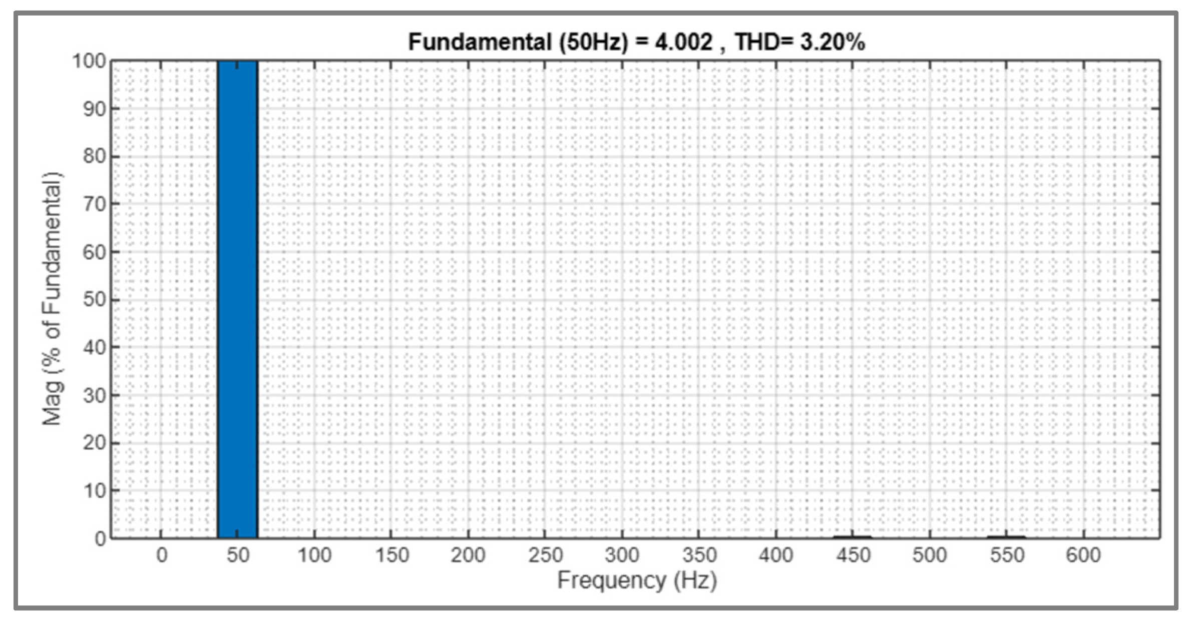
| Proposed MLI | 25 | 11 | 11 | 4 | - | - | 1.04 | 2.43 | 3.20 | 1.09 | 1.19 |
| Parameter | Trade-Off Consideration | Justification |
|---|---|---|
| Total Standing Voltage (TSV) | Moderate Reduction | Lower TSV improves switch reliability, but excessive reduction increases component count and cost. |
| Component Count | Minimized | Fewer components reduce system complexity and improve cost-effectiveness. |
| Cost Function | High Priority | Optimized to ensure an affordable and scalable design. |
| Harmonic Performance (THD) | Balanced | Achieved through effective modulation strategies without adding extra hardware. |
| Switching Losses | Moderate Control | Switching frequency and modulation schemes help mitigate energy losses. |
| Parameter | 15-Level | 25-Level | ||
|---|---|---|---|---|
| R Load | R-L Load | R Load | R-L Load | |
| VRMS | 282.82 V | 282.82 V | 282.82 V | 282.82 V |
| IRMS | 2.82 A | 4.80 A | 2.82 A | 4.80 A |
| POUT | 797.55 W | 1357.54 W | 797.55 W | 1357.54 W |
| PCL | 53.60 W | 133.06 W | 53.60 W | 133.06 W |
| PSL | 0.22 W | 0.37 W | 0.37 W | 0.62 W |
| PTL | 53.82 W | 133.43 W | 53.97 W | 133.68 W |
| PIN | 851.37 W | 1490.97 W | 851.52 W | 1491.22 W |
| η | 93.68% | 91.05% | 93.66% | 91.03% |
| 15-Level | 25-Level | ||
|---|---|---|---|
| Reference | η | Reference | η |
| [43] | 90.0% | [30] | --- |
| [44] | 93.7% | [31] | 93.8% |
| [45] | * 90.0% | [32] | * 96.5% |
| [46] | --- | [33] | --- |
| Proposed | * 93.7% | [34] | * 92.5% |
| [35] | * 92.5% | ||
| [36] | 95.0% | ||
| Proposed | * 93.7% | ||
Disclaimer/Publisher’s Note: The statements, opinions and data contained in all publications are solely those of the individual author(s) and contributor(s) and not of MDPI and/or the editor(s). MDPI and/or the editor(s) disclaim responsibility for any injury to people or property resulting from any ideas, methods, instructions or products referred to in the content. |
© 2025 by the authors. Licensee MDPI, Basel, Switzerland. This article is an open access article distributed under the terms and conditions of the Creative Commons Attribution (CC BY) license (https://creativecommons.org/licenses/by/4.0/).
Share and Cite
Bandahalli Mallappa, P.K.; Velasco-Quesada, G.; Martínez-García, H. Design and Analysis of 15-Level and 25-Level Asymmetrical Multilevel Inverter Topologies. Electronics 2025, 14, 1416. https://doi.org/10.3390/electronics14071416
Bandahalli Mallappa PK, Velasco-Quesada G, Martínez-García H. Design and Analysis of 15-Level and 25-Level Asymmetrical Multilevel Inverter Topologies. Electronics. 2025; 14(7):1416. https://doi.org/10.3390/electronics14071416
Chicago/Turabian StyleBandahalli Mallappa, Prasad Kumar, Guillermo Velasco-Quesada, and Herminio Martínez-García. 2025. "Design and Analysis of 15-Level and 25-Level Asymmetrical Multilevel Inverter Topologies" Electronics 14, no. 7: 1416. https://doi.org/10.3390/electronics14071416
APA StyleBandahalli Mallappa, P. K., Velasco-Quesada, G., & Martínez-García, H. (2025). Design and Analysis of 15-Level and 25-Level Asymmetrical Multilevel Inverter Topologies. Electronics, 14(7), 1416. https://doi.org/10.3390/electronics14071416